Abstract
In this brief paper, the dependency of short-circuit power on threshold voltage is analyzed and utilized for short circuit (SC) power reduction in multi-threshold (MTCMOS) processes. Analytical expressions are developed for estimation of the change of ratio between short-circuit power and dynamic power (PSC/Pdyn) while changing the design process. The analysis shows that the PSC/Pdyn ratio can increase significantly if the VT/Vdd ratio in new process decreases. An analytical expression is also derived for estimation of potential SC power reduction in MTCMOS processes by replacing low-VT transistors by high-VT devices in the same process. The proposed technique allows significant reduction of SC power without the need for process shift. The simulation results show good correlation with the analytical estimation at cell level, while demonstrating an average SC power saving of 36%. The performance impact is also validated, showing that timing degradation is minor and controllable. The proposed optimization technique is applicable to any multi-threshold process. The technique is simple for implementation, and can be easily integrated in the existing optimization tools.
1. Introduction
The power reduction in VLSI circuits is becoming one of the key challenges in the semiconductors industry. The techniques for power optimization are applied at all levels of semiconductor design. The advanced processors feature multiple improvements at architectural level, like branch prediction, software-hardware co-optimization, utilization of multiple cores in one processor, and more. At system level, multiple power planes are used enabling low-power operating points, efficient power control and shut off of inactive blocks. The power control can be obtained during the operation, such as in the case of various thermal sensors embedded in 32 nm Sandy Bridge processor; or even during production testing, as in the case of controlling the effective size of pull-up devices for low-voltage cache operation [1]. Additional techniques are applied at system level to block levels to optimize the power consumed by the clock tree. The high activity and capacitance of the clock tree, together with its importance and influence on the performance and reliability of the processor, make the clock optimization an important component of overall power optimization. Techniques like clock gating, skew optimization, retiming and others are being extensively used in advanced designs. At circuit level, techniques for low-power logic gates implementation can be used [2] to allow reduced power and area, without compromising the performance. Finally, the most important impact on power reduction is achieved by advances in the semiconductor process technologies. By providing new MOS structures, like 3D transistors [3]; or by enabling a multiple choice of threshold voltages for the circuits, the advanced manufacturing processes allow the exponential improvement in performance, dictated by Moore’s low, while maintaining the power budgets of the designs. A change of the manufacturing process is, however, an expensive and complex move. The designer must fully utilize the potential of power optimization allowed by a given process, before considering a shift to a new technology.
A common characteristic of the effective power optimization techniques at all the levels is the high impact and wide application of the technique over the design. The most efficient techniques should be applied orthogonally to other optimizations, and should not influence the design flow, maintain the performance, and require minimal or no changes in the standard cell libraries and tools. Moreover, it is important to distinguish between the various components of power consumption and reduce certain power components without increasing other.
The total power dissipation of a logic cell can be described as follows:

where Pleak is the power consumed during the steady-state period, and Pactive is the power dissipated during logic transitions and is comprised of two components: the dynamic power Pdyn and theshort-circuit power PSC. The leakage power is consumed by closed devices while no transitions occur and, thus, is regarded as parasitic power. The dynamic power Pdyn is dissipated while charging/discharging the capacitances. This power dominates the total power value in most of applications and is regarded as useful, as it contributes to transition of logic signals. The short-circuit power PSC is dissipated due to a temporary direct path between Vdd and gnd during simultaneous conduction of both p- and n-block of CMOS cell. Opposed to the dynamic power, the short-circuit power is considered as waste, as it does not contribute to signal transitions.
2. Short Circuit Power Analysis and Optimization
The mechanism of short-circuit power dissipation is depicted in Figure 1 for a CMOS inverter. During an input transition, there will be a time period in which both the NMOS and PMOS will conduct, causing short-circuit current to flow from supply to ground. This current flows within a time “window”, where input voltage is higher than a threshold voltage of NMOS VTn (keeping NMOS on), and lower than a threshold voltage of PMOS VTp below Vdd (keeping PMOS on). The duration and the magnitude of the SC current depend directly on the slope of the input signal. In addition, there is a dependency on the output slope, while the short-circuit current grows as the output slope is substantially smaller than the input slope. This is caused by the fact that the drain-source voltage of the closing transistor equals to Vdd most of the transition time, leading to the maximal short-circuit current (saturation) [4].

Figure 1.
Short-circuit current in CMOS inverter.
Figure 1.
Short-circuit current in CMOS inverter.

In many cases, the SC power is neglected during the analysis of power dissipation, or during development of power optimization techniques [5]. However, the portion of the SC power out of the dynamic power can be significant. While in some cases it is assumed to be around 10% of the dynamic power [6], the high dependency of the SC power on slopes may cause an increase of SC to tens of percents out of dynamic power [7].
One of the challenges in SC analysis is the separate estimation of SC power. Some works propose analytical models for SC estimation [8]. However, these models are complex for manual usage or for fast estimation of SC portion out of dynamic power. Other researches propose estimation of PSC/Pdyn ratio based on empirical simulations [9]. The research in [7] shows the dependency of the SC on the process parameters as part of technology scaling, without addressing MTCMOS processes.
Another challenge is related to SC power optimization. In many researches targeting power optimization, the SC power is neglected, while in some cases the SC reduction is a by-product of dynamic or leakage power optimization. Similar situation can be observed in industrial designs, where major focus is applied on dynamic and leakage power reduction. Indeed, some of the techniques for SC reduction are similar to common low-power design measures. The downsizing of transistors contributes to SC reduction, but is an integral part of most of the existing optimization techniques, both for leakage and for dynamic power. Similarly, the voltage scaling can be effective for overall power reduction and will reduce the absolute values of the SC power, but is not effective for reduction of PSC/Pdyn ratio, as was shown in [7,10]. The approach of slope-balancing proves to be effective for SC power reduction [11]. However, in many cases this is a side effect of global sizing optimizations in which the oversized transistors are identified and treated, while resolving timing requirements. These techniques are usually basing on existing power characteristics in which the overall active power is given including both PSC and Pdyn components. As most of the aforementioned techniques for dynamic power reduction are already a part of a standard design flow, in order to gain additional power reduction, there is a need for specific optimizations focusing on SC power, without increasing the dynamic and leakage power and without compromising the timing.
In [7] the SC reduction was addressed with regards to technology scaling, while showing the dependency of SC on the threshold voltage of the process. However, in this work the SC reduction is achieved by similar measures as leakage reduction, and becomes significant only for high frequencies. Moreover, the SC reduction in this work is allowed only as part of process technology scaling rather than optimizing a design in a given process. This, of course, is an extremely costly solution for most industrial designs.
In order to target the SC power optimization effectively, there is a need for separate estimation of the SC power both as absolute value and as portion of the active power. It is important to insure that the SC optimization does not increase other power components and maintains the timing requirements of the design. As most of the industrial designs are based on standard cell libraries with wide variety of cells, for effective utilization of the technique it is also desirable that it would be template-independent and widely applicable.
In this brief paper we present a technique for SC power reduction by using high-VT transistors in multi-threshold processes. This technique allows a dedicated approach for SC optimization by utilizing the VT-dependency of the SC power, while resolving the aforementioned challenges and fulfilling the timing and design methodology requirements. Expressions are developed for analyzing the SC power dependency on VT and deriving the ratio of SC power out of dynamic power. The simulation results of SC reduction are presented, followed by discussion.
3. Short Circuit Power Dependency on VT
As was shown in Figure 1 the short circuit power is dissipated during the transition period of the input signal and is dependent on the current magnitude and the input slope duration. A model for SC current estimation developed by Veendrick in [11] is widely used as handy model of SC power dissipation:

The formula describes the short-circuit power dissipation in a CMOS inverter without output load, where β is the gain factor, τ is the input rise/fall time of inverter and T is the input signal period. An intuitive description of the cubic SC current dependency on the threshold voltage is also shown in Figure 1. As can be seen, the duration of the SC current linearly depends on the threshold voltages, while the maximal SC current has a quadratic dependency on threshold voltage. Note that this model assumes square law saturation, but the expressions developed here can also be extended to velocity saturation models.
Here, we develop the formula in order to derive analytical metrics describing the process-dependency of PSC/Pdyn ratio, as well as the dependency of SC power on the threshold voltage in a given process. The Formula (2) can be transformed by estimating the rise/fall time in terms of effective resistance and capacitance of the inverter:

where R0 is the effective resistance of the driver, C0 is the input capacitance of the cell on which power is measured. The factor α describes the fact that the rise/fall time definition in (2) is from 0% to 100% of voltage swing [11], and that there is generally a size ratio between the gate capacitance of the driver and the driven cell.
We also define relationship between the supply voltage and the threshold voltage as follows:

where x is the ratio between VT and Vdd in a given process.
Now, we can express the dependency of PSC on threshold voltage in a given process, by using the expressions in (3) and (4):

where f is the input signal frequency defined as 1/(2T).
The dynamic power consumption is defined by:

The ratio between the dynamic and short-circuit power in various processes is obtained by substitution of (6) into (5), leading to the following expression:

As can be seen, there is cubic dependency of the PSC/Pdyn ratio on the VT/Vdd ratio of the process. The power ratio dependency on supply voltage is eliminated, when taking into account the voltage dependency of β and R0 (supporting the results in [7,8]).
4. Short-Circuit Power Reduction by High-VT Transistors
As was shown in (7), the SC power strongly depends on the threshold voltage and can change significantly while moving to a new process. This characteristic can be utilized for SC power optimization in modern multi-threshold processes. One of the main reasons for maintaining devices with various threshold voltages in same process is the leakage reduction when using high-VT (HVT) devices in non-critical paths. Alternatively, the leakage reduction is achieved in many processes by using long-length (LL) transistors. These devices usually operate with lower threshold voltage than high-VT transistors, but allow leakage reduction due to longer channels. Both transistor types can be considered for low-power designs while maintaining a similar performance and leakage power.
The long-channel devices are popular choice for low-leakage design in modern processes. However, due to lower threshold voltages, they are less effective in terms of short-circuit. This fact creates an opportunity for SC power optimization in designs with LL transistors, by replacing the long-length transistors with high-threshold transistors in MTCMOS processes. Due to the aforementioned properties of the devices, the leakage and the timing of the replaced cells can be maintained similar, while reducing the SC power consumption.
This optimization is orthogonal to the existing techniques of power reduction. Thus, by replacing the long-length transistors by high-VT transistors, we expect to obtain a reduction in PSC/Pdyn ratio. Using (7), the PSC/Pdyn ratio can be written as:

We can estimate the SC reduction by comparing the ratio for original vs. high-VT devices:

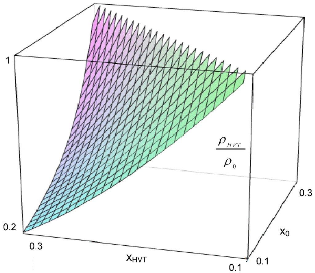
Figure 2 shows the potential PSC/Pdyn ratio reduction by using various ratios of VT/Vdd during replacement of transistors by higher-VT devices. Note that for ranges of 0.1 < x0 < 0.3 and 0.1 < xHVT < 0.3, up-to 80% reduction of SC power can be achieved (without changing the Vdd).

Figure 2.
The PSC/Pdyn ratio reduction by using transistors with higher VT/Vdd ratio.
Figure 2.
The PSC/Pdyn ratio reduction by using transistors with higher VT/Vdd ratio.

By substituting the corresponding process parameters into (9), we may expect a reduction of about 40% in SC power obtained by using HVT devices instead of LL. Note that the VT change does not influence the dynamic power, since the Vdd and the overall capacitance remains unchanged. Thus, the PSC/Pdyn ratio reduction is translated directly into 40% SC power reduction.
Note that similar optimization may be performed by replacing nominal transistors by high-VT. However, in such case the timing degradation will be more substantial and the replacement has to be performed carefully to avoid impact on critical paths. In this work we perform only LL-to-HVT replacement.
5. Simulation Results
A proprietary simulation-based power estimation tool was used in this work for power simulation and separate estimation of SC power. The SC power is estimated by subtracting the dynamic power portion from the simulated active power. The leakage power is also separately measured.
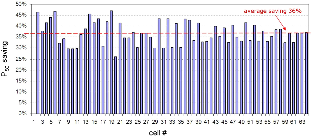
In order to validate the efficiency of the proposed technique, a sample data-path design was used. In the selected design, 63 LL cells were eligible for replacement by HVT according to design methodology constraints. The transistor models were replaced without changing the size of the devices. Power simulation was performed on the design before and after the replacement to assess the SC power reduction. The set of the optimized cells was comprised of inverters and combinatorial CMOS cells (no sequentials were included in this experiment). The SC power reduction in each cell is shown in Figure 3.

Figure 3.
Cell-level SC power saving by replacing long-length (LL) cells by high-VT (HVT). The average saving of 36% is in good correlation with theoretical estimations.
Figure 3.
Cell-level SC power saving by replacing long-length (LL) cells by high-VT (HVT). The average saving of 36% is in good correlation with theoretical estimations.

As can be seen, the SC power was reduced significantly in all the cells. The power reduction in most of the cells varied from 30% to 45%, while the average SC power saving was 36%. These results are in a good correlation with the theoretical prediction of 40% reduction in (9). The variations in the power saving ratio can be related to the slopein/slopeout differences of each cell.
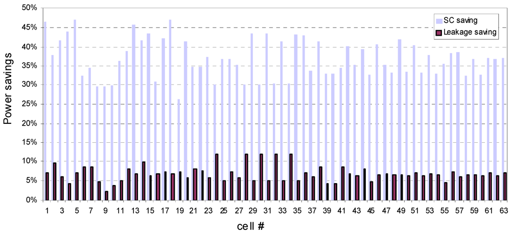
As was mentioned above, the main purpose of LL cells is leakage reduction. Thus, it is important to check that the leakage power was not increased as the result of the SC optimization. Thus, the leakage power consumption before and after optimization was separately estimated and was compared in Figure 4. As can be seen, the leakage power was decreased while changing the models from LL to HVT in all the cells. The average leakage power reduction in the optimized cells is 6.9%.
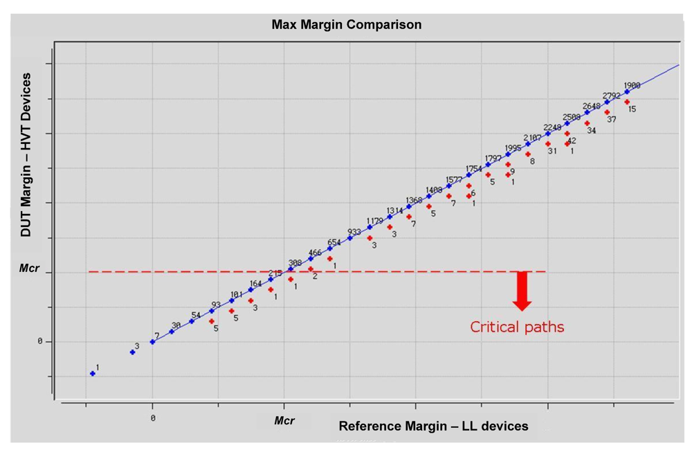
The substitution of LL transistors by HVT may have an impact on timing parameters. The exact performance difference between the two types of transistor depends on the process technology parameters, but usually there is some increase in delay while switching to HVT transistors. Thus, the timing impact of the SC power reduction by HVT transistors was also validated. For this purpose a timing analysis was performed in the design before and after the optimization, using static timing analyzer. The resulting margins of the design were then compared, as shown in Figure 5. The plot presents the distribution of the logic paths in the design according to the time margin of each path. The X axis is the original margin of the paths before optimization. The Y axis shows the margins of the corresponding paths after HVT optimization. The paths with same margin value are grouped together, so that each point represents a group of paths with same margin and the corresponding number represents the number of paths in each margin group. The blue points on the diagonal line are paths in which no margin change occurred. The red points, below the diagonal, represent path groups which experienced margin degradation. As can be seen, relatively few paths have been influenced by the optimization. Moreover, only in 15 paths out of thousands the margins were reduced below a critical margin value Mcr. Note that in a practical case, the cells influencing these paths can be easily excluded from the optimization flow. Thus, the timing impact of the technique is minor and controllable.

Figure 4.
Average leakage power reduction of 6.9% was observed in HVT cells as compared to LL.
Figure 4.
Average leakage power reduction of 6.9% was observed in HVT cells as compared to LL.


Figure 5.
Timing analysis of the design after replacing LL transistors by HVT. The performance degradation due to the optimization is minimal.
Figure 5.
Timing analysis of the design after replacing LL transistors by HVT. The performance degradation due to the optimization is minimal.

An additional advantage of a good correlation with the theoretical estimation, coupled with the minor timing impact, is the ability to estimate the power reduction potential of the design based only on initial power metrics. This can be done by applying the SC reduction factor from (9) to each eligible cell, without the need for actual model replacement and simulation. In this manner the overall power reduction potential can be easily estimated, and optimization sensitivity of various design blocks can be assessed.
6. Summary
The dependency of short-circuit power on threshold voltage was analyzed and utilized for SC power reduction in MTCMOS processes. Analytical expressions were developed to allow handy estimation of the PSC/Pdyn ratio. The results show that the PSC/Pdyn ratio can increase significantly if the VT/Vdd ratio in the new process decreases. An analytical expression was derived for estimation of potential SC power reduction in MTCMOS processes. The replacement of low-VT transistors by high-VT devices in same process allows significant reduction of SC power without the need for process shift. In addition, there is no impact on dynamic power consumption, and some reduction of leakage is possible as by-product. The simulation results of optimization in 63 cells showed good correlation with the analytical estimation, while demonstrating an average SC power saving of 36%, compared to 40% saving estimation by using analytical Formula (8). The performance impact was also validated, showing that timing degradation is minor and controllable.
The proposed technique for SC power reduction by high-VT transistors is applicable to any multi-threshold process. As has been shown, higher difference in threshold voltage of the process models, allows higher SC power saving. The advantages of the technique are that it does not have area cost and does not increase other power components. Trading between the different models of low-leakage transistors may have an impact on performance. However, timing analysis shows that the change in time margins across the design is minor and can be controlled by selectively applying the technique to non-critical paths.
The implementation effort of the technique is low. It can be easily integrated within existing optimization tools. In its basic form, the identification of the candidate cells for optimization is based only on margin data, which is available from static timing analysis. Thus, no significant computational complexity or run time increase are expected. This should allow simple integration of the technique in existing industrial design flows.
References
- Yuffe, M.; Knoll, E.; Mehalel, M.; Shor, J.; Kurts, T. A Fully Integrated Multi-CPU, GPU and Memory Controller 32 nm Processor. In Proceedings of IEEE International Solid-State Circuits Conference (ISSCC), San Francisco, CA, USA, 19–23 February 2011.
- Morgenshtein, A.; Shwartz, I.; Fish, A. Gate Diffusion Input (GDI) logic in standard CMOS nanoscale process. In Proceedings of the IEEE 26th Convention of Electrical and Electronics Engineers in Isreal (IEEEI), Eliat, Isreal, 17–20 November 2010.
- Intel 22nm 3-D Tri-Gate Transistor Technology. Available online: http://newsroom.intel.com/docs/DOC-2032 (accessed on 20 December 2011).
- Rabaey, J.M.; Chandrakasan, A.; Nikolic, B. Digital Integrated Circuits: A Design Perspective; Prentice Hall Int.: Upper Saddle River, NJ, USA, 1996. [Google Scholar]
- Nose, K.; Sakurai, T. Optimization of VDD and VTH for low-power and high speed applications. In Proceedings of the Conference on Asia South Pacific Design Automation Conference, Yokohama, Japan, 25–28 January 2000; pp. 469–474.
- Chandrakasan, A.P.; Sheng, S.; Brodersen, R.W. Low-Power CMOS Digital Design. IEEE J. Solid State Circuit 1992, 27, 473–484. [Google Scholar]
- Chatterjee, A.; Nandakumar, M.; Chen, I. An investigation of the impact of technology scaling on power wasted as short-circuit current in low voltage static CMOS circuits. In Proceedings of the International Symposium on Low Power Electronics and Design, Mnonterey, CA, USA, 12–14 August 1996; pp. 145–150.
- Nose, K.; Sakurai, T. Closed-Form Expressions for Short-Circuit Power of Short-Channel CMOS Gates and its Scaling Characteristics. In Proceedings of the International Technical Conference on Circuits/Systems, Computers and Communications; Sokcho, Korea: July 1998; pp. 1741–1744.
- Alvandpour, A.; Larsson-Edefors, P.; Svensson, C. Separation and extraction of short-circuit power consumption in digital CMOS VLSI circuits. In Proceedings of the International Symposium on Low Power Electronics and Design, Mnonterey, CA, USA, 10–12 August 1998; pp. 245–249.
- Nose, K.; Sakurai, T. Analysis and Future Trend of Short-Circuit Power. IEEE Trans. Comput. Aided Design Integr. Circuits Syst. 2000, 19, 1023–1030. [Google Scholar] [CrossRef]
- Veendrick, H.J.M. Short-Circuit Dissipation of Static CMOS Circuitry and its Impact on the Design of Buffer Circuits. IEEE J. Solid State Circuit 1984, sc-19, 468–473. [Google Scholar] [CrossRef]
© 2012 by the authors; licensee MDPI, Basel, Switzerland. This article is an open-access article distributed under the terms and conditions of the Creative Commons Attribution license (http://creativecommons.org/licenses/by/3.0/).
