CMOS Leakage and Power Reduction in Transistors and Circuits: Process and Layout Considerations

Abstract
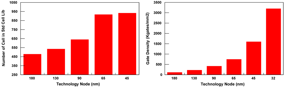
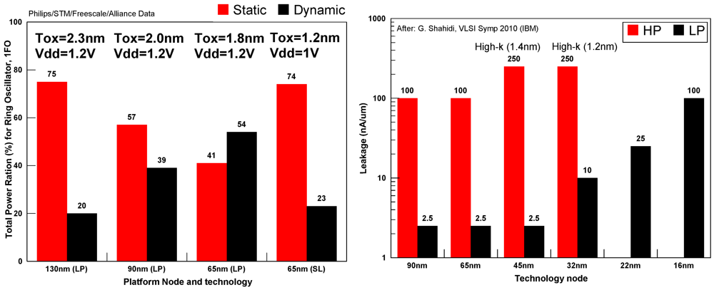
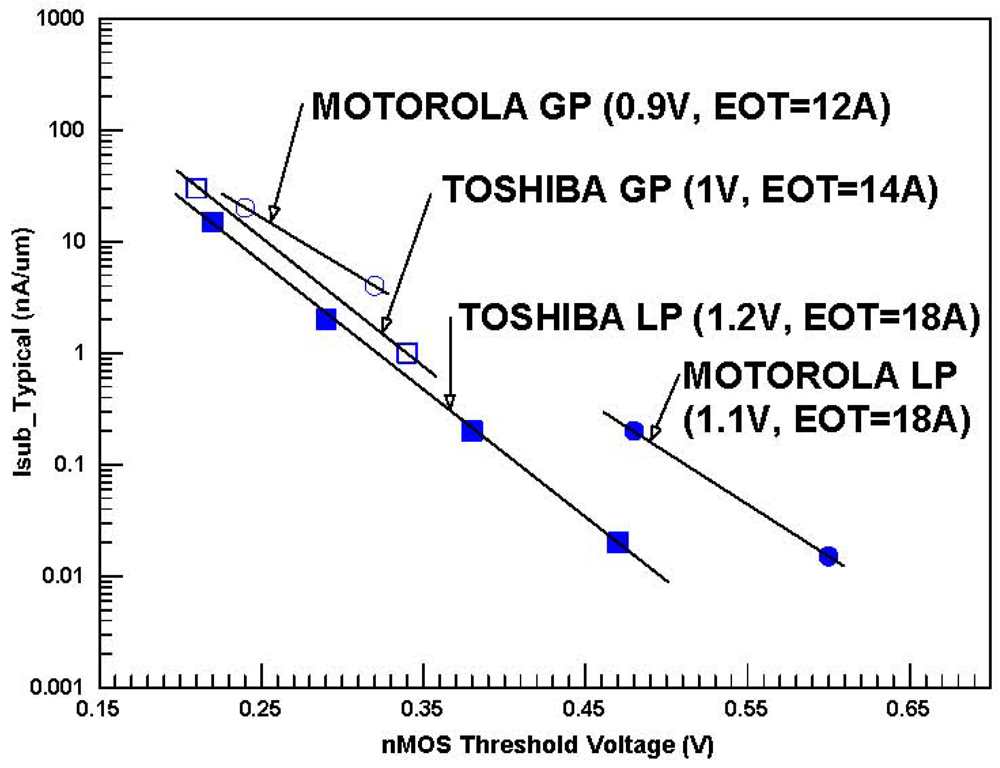
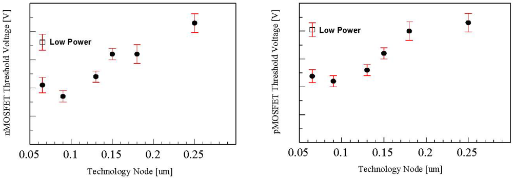
:1. Introduction

| Platform (node) | 65 nm | 45 nm | 40 nm | 32 nm | ||||||||||
| Technology Application | Standard Logic for General Purposes | Low Power | High Performance LP | LP for mobile/WiFi | General Purpose—High-Performance | |||||||||
| Vdd (V) | 1 | 1.2 | 1 | 1.1 | 0.9 | |||||||||
| Stressors | SMT, SiGe, cSEL | SMT, cSEL | SMT, SiGe, cSEL | |||||||||||
| Gate Formation | Poly/SiON | Poly/SiON | Poly/SiON | HK/MG | ||||||||||
| Reference | ST, NXP, CEA-LETI Minatec [1] | Fujitsu [3] | TOSHIBA [4] | IBM Alliance [5] | ||||||||||
| Tox_Inv N/P (Å) | 20.5/22.5 | 26/27.5 | 19.1/20.5 | 24.5/25.5 | 12/14 | |||||||||
| Vt Type | HVt | SVt | LVt | HVt | SVt | LVt | HVt | SVt | HVt | SVt | LVt | HVt | SVt | LVt |
| Ion_N/Ion_P (μA/μm) | 670/295 | 830/398 | 950/450 | 420/210 | 610/310 | 740/390 | 970/630 | 1220/765 | 487/235 | 715/295 | 840/370 | 855/550 | 1050/650 | 1250/790 |
| Isub_N/Isub_P (nA/μm) | 5/3 | 51/40 | 130/130 | 0.015/0.009 | 0.36/0.10 | 5/2.5 | 10/10 | 100/100 | 0.03/0.03 | 0.4/0.4 | 6/3 | 1/1 | 10/10 | 100/100 |
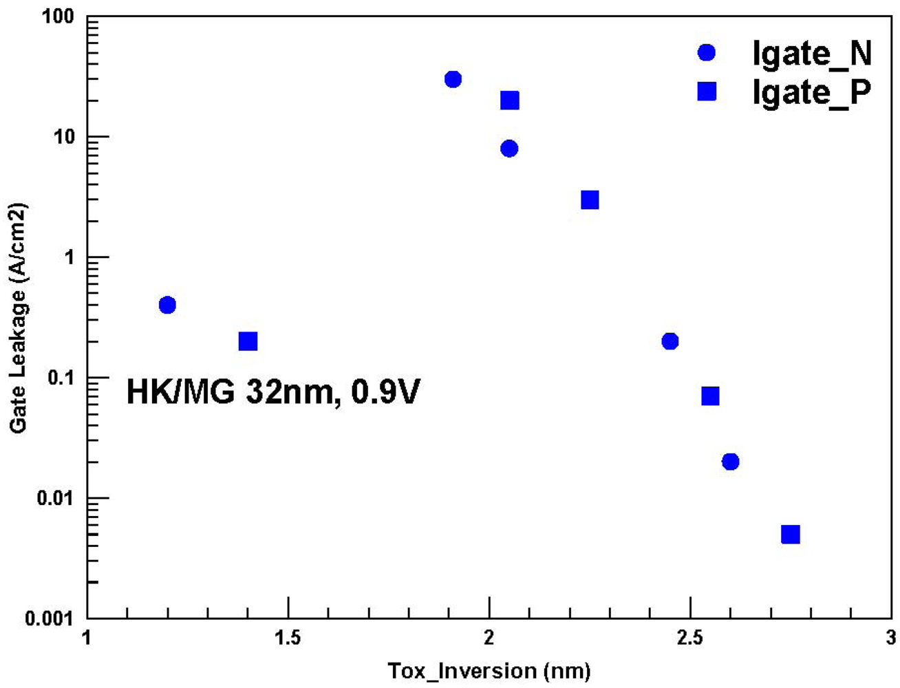
| Igate_N/Igate_P (A/cm2) | 8/3 | 0.02/0.005 | 30/20 | 0.2/0.07 | 0.4/0.2 | |||||||||
| Gate Delay RO 1FO (ps/gate) | 14 | 10.5 | 8.8 | 25.5 | 17.5 | 13.5 | ||||||||

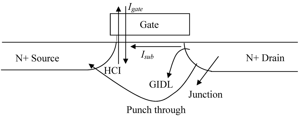
2. Transistors Leakage Components

3. Transistor and Cell Level Leakage Analysis and Optimization
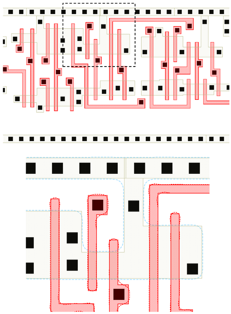
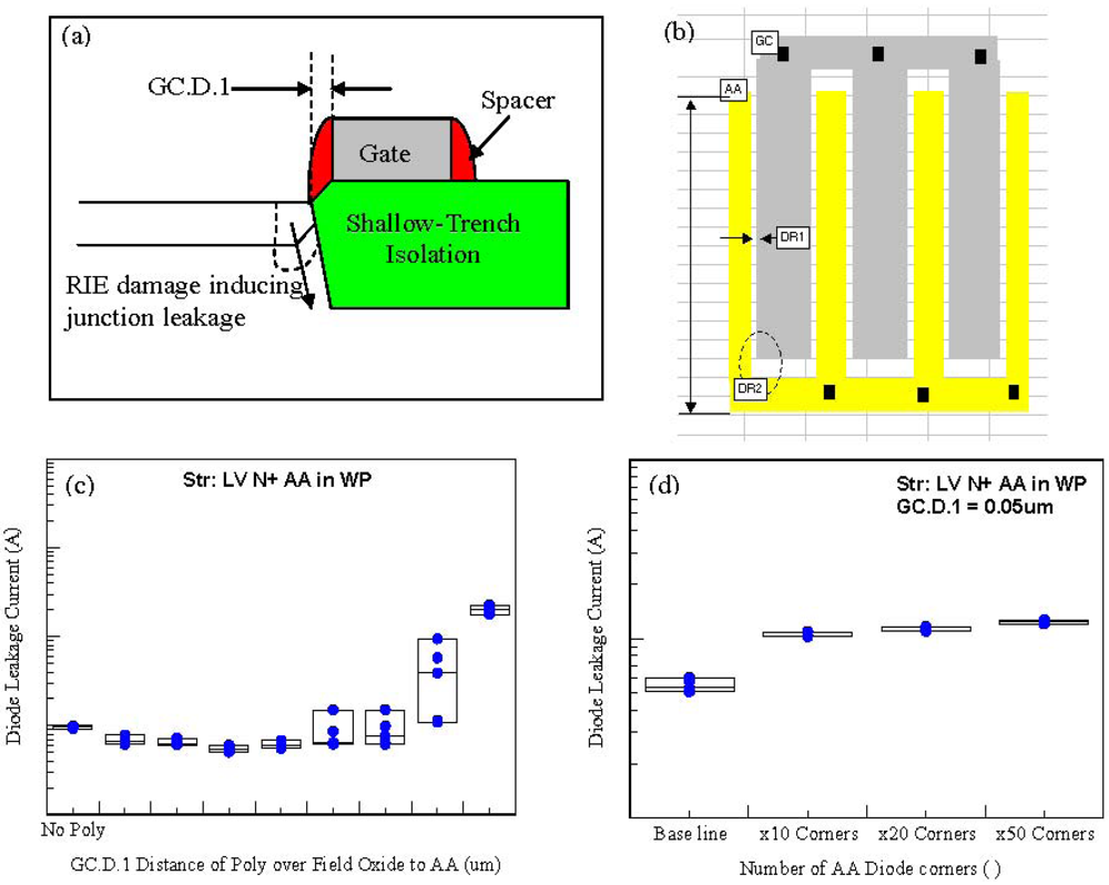
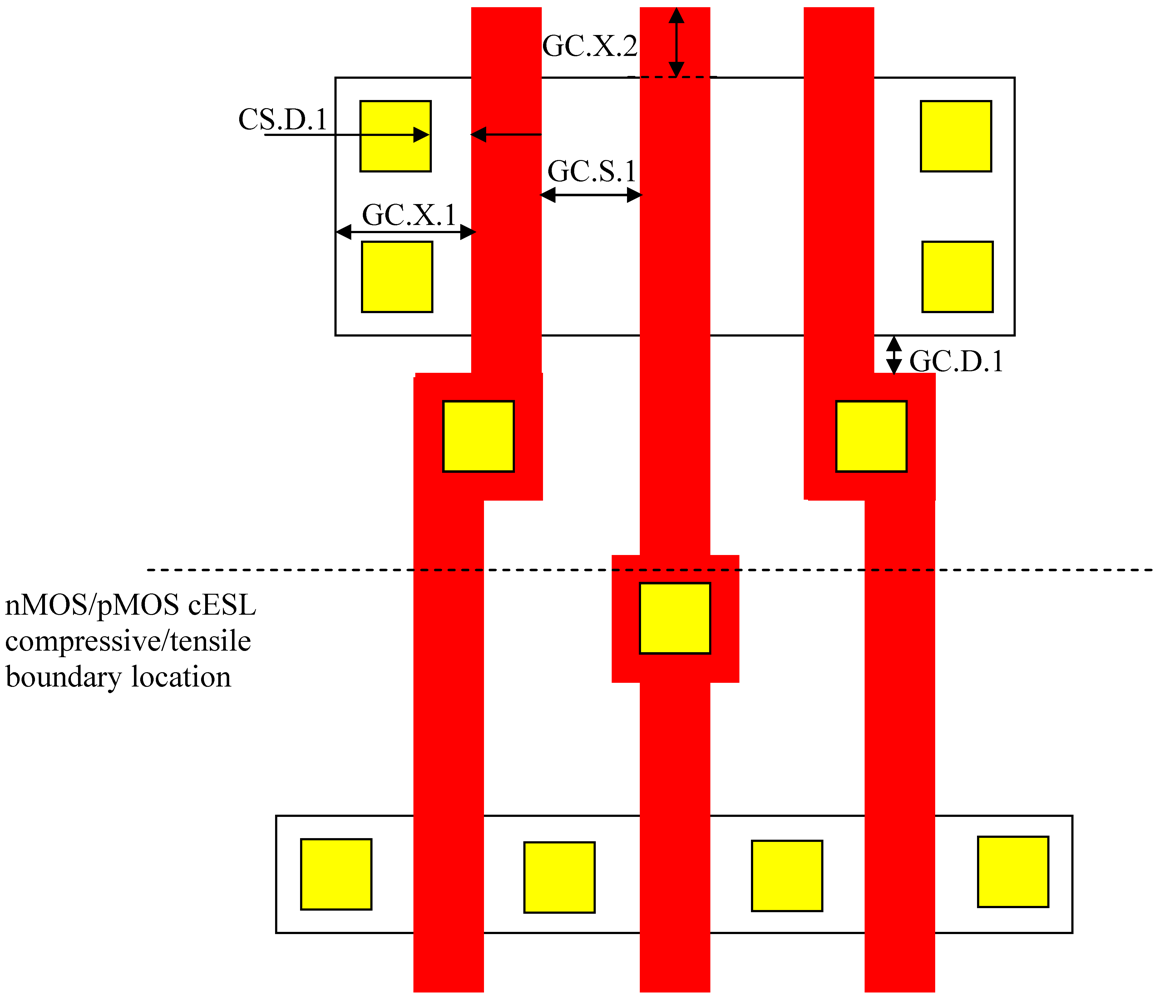
3.1. Topological Design Rules and Layout Optimization

| Rule | Design Rule Description | 180 nm | 130 nm | 90 nm | 65 nm |
|---|---|---|---|---|---|
| GC.D.1 | Distance of Poly (over STI) to related AA | 0.10 | 0.07 | 0.05 | 0.05 |
| GC.X.2 | Extension of poly beyond AA (end-cap) | 0.22 | 0.18 | 0.16 | 0.14 |
| AA.D.3 | Distance between WN to N+ in WP | 0.43 | 0.34 | 0.22 | 0.16 |
| AA.E.3 | Enclosure of WN around P+ in WN | 0.43 | 0.34 | 0.22 | 0.16 |
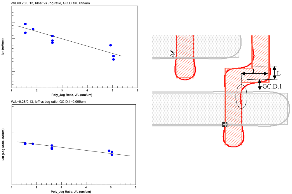
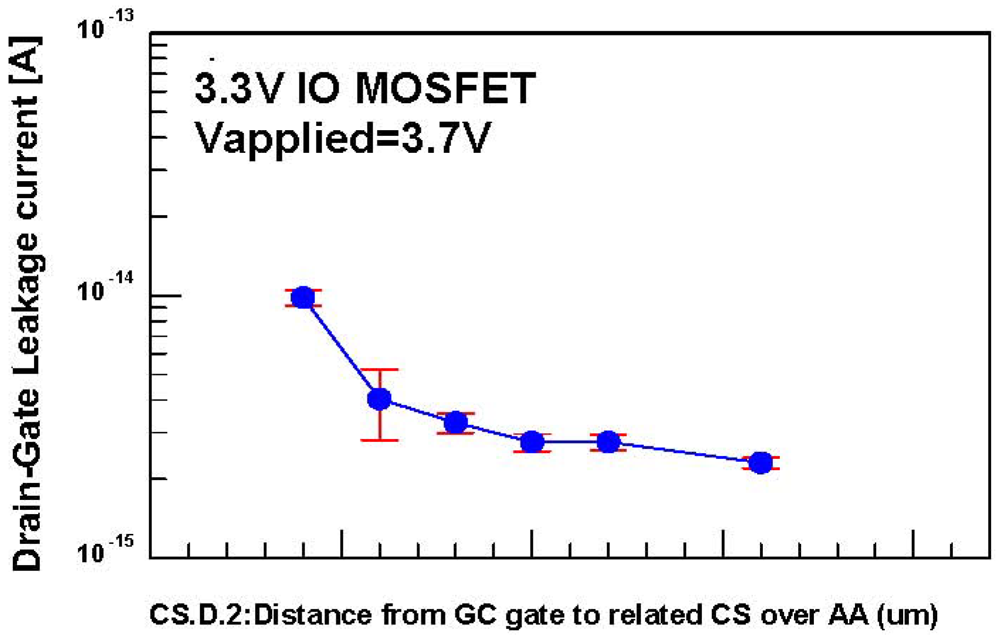
| CS.D.1/2 | Distance of CS over AA to related Gate | 0.16 | 0.11 | 0.11 | 0.09 |


| Rule | Rule Description | Rule Weight | A | B1 | B2 | C |
|---|---|---|---|---|---|---|
| RGC.D.1 | Distance between Poly (over STI) to AA Edge | 8 | 86.10% | 82.80% | 88.80% | 98.40% |
| RCS.D.1 | Distance between CS to Poly gate | 7 | 83.70% | 84.20% | 84.20% | 91.50% |

3.2. Leakage Reduction in Transistor Level—CMOS and SRAM


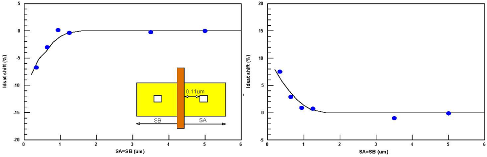
- • Expending the AA (Source and Drain) edges beyond gate (GC.X.1), for different STI induce stress (Figure 15). The stress range and magnitude are up to GC.X.1 = 1.3 μm, and <10%, respectively;
- • Re-placement of contacts with distance to gate (CS.D.1). This is because contacts “punching” of the cSEL layer, and release some of the stress. For this reason, also re-set of the Source and Drain contact pitch may improve performance [37];


| 12 Circuit | Number of Gates | Comparison for Iso-Delay Against Only Dual- Vt Assignment | Comparison for Iso-Leakage Against Only Dual- Vt Assignment | ||||||
|---|---|---|---|---|---|---|---|---|---|
| Stress + Vt based assignment | Only stress based assignment | Stress + Vt based assignment | Only stress based assignment | ||||||
| Improvement in Leakage | Area Overhead | Improvement in Leakage | Area Overhead | Improvement in Delay | Area Overhead | Improvement in Delay | Area Overhead | ||
| Minimum | 14.70% | 0.10% | 4.70% | 0.20% | 4.60% | 0.20% | 2.30% | 0.20% | |
| Median | 22.45% | 0.30% | 5.10% | 0.35% | 5.10% | 0.30% | 2.95% | 0.35% | |
| Maximum | 38.50% | 0.90% | 12.00% | 0.90% | 5.80% | 0.90% | 3.60% | 1.00% | |
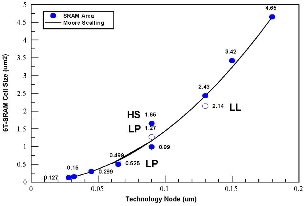
4. Low Power Consideration for SRAM


5. Circuit Level Techniques for Power and Leakage Reduction
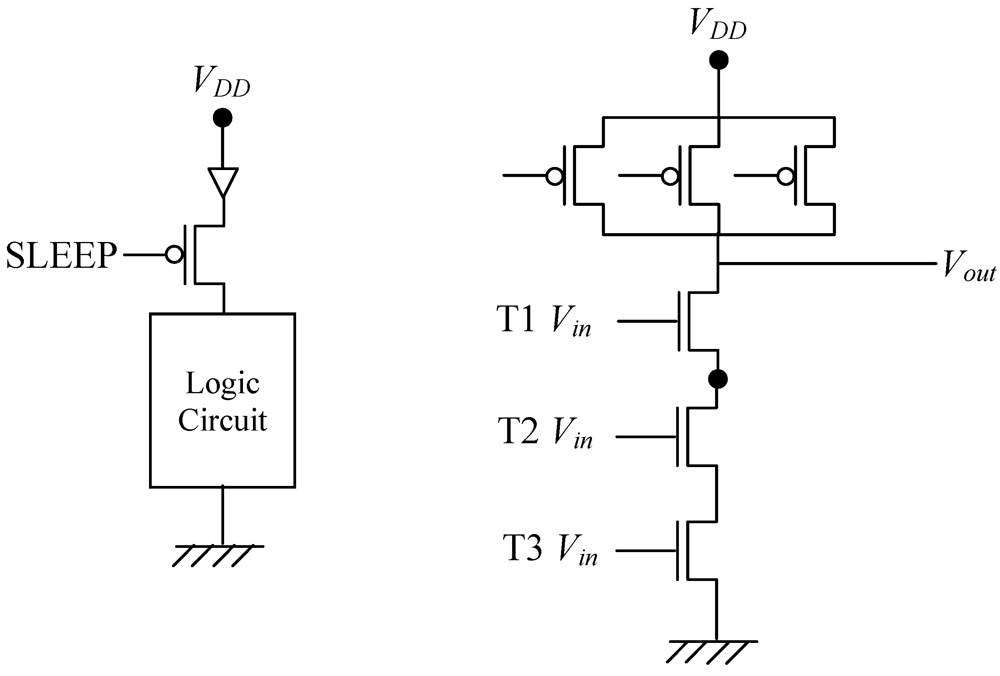
- • The Delay rule—within mixed stack, the L-Vt Transistor (with low Vt doping and thin oxide), has to be placed as close as possible to the gate output to achieve best results for the time delay;
- • The leakage rule—within mixed stack, the H-Vt Transistor (having high Vt doping and thick oxide), has to be placed at the end of the stack (away from the output) to achieve best leakage result.
| Realization Combination # | pMOS Transistors | nMOS Transistors | Relative Leakage | Relative Gate Delay |
|---|---|---|---|---|
| 1 | LLL | T1 = L, T2 = L, T3 = L | 100% | 100 |
| 2 | HHH | T1 = L, T2 = H, T3 = L | 50% | 118% |
| 3 | T1 = H, T2 = L, T3 = L | 50% | 124% | |
| 4 | T1 = L, T2 = H, T3 = H | 30% | 126% |

6. Summary and Conclusions
Acknowledgment
References
- Skotnicki, T.; Fenouillet-Beranger, C.; Gallon, C.; Boeuf, F.; Monfray, S.; Payet, F.; Pouydebasque, A.; Szczap, M.; Farcy, A.; Arnaud, F.; et al. Innovative materials, devices, and CMOS technologies for low-power mobile multimedia. IEEE Trans. Electron Device 2008, 55, 96–130. [Google Scholar]
- Tavel, B.; Duriez, B.; Gwoziecki, R.; Basso, M.T.; Julien, C.; Ortolland, C.; Laplanche, Y.; Fox, R.; Sabouret, E.; Detcheverry, C.; et al. 65 nm LP/GP Mix Low Cost Platform for Multi-Media Wireless and Consumer Applications. In Proceedings of the 35th European Solid-State Device Research Conference (ESSDERC 2005), Grenoble, France, 12–16 September 2005; 50, pp. 573–578.
- Miyashita, T.; Ikeda, K.; Kim, Y.S.; Yamamoto, T.; Sambonsugi, Y.; Ochimizu, H.; Sakoda, T.; Okuno, M.; Minakata, H.; Ohta, H.; et al. High-Performance and Low-Power Bulk Logic Platform Utilizing FET Specific Multiple-Stressors with Highly Enhanced Strain and Full-Porous Low-k Interconnects for 45-nm CMOS Technology. In Proceedings of the IEEE International Electron Devices Meeting, (IEDM 2007), Washington, DC, USA, 10–12 December 2007; pp. 251–254.
- Watanabe, R.; Oishi, A.; Sanuki, T.; Kimijima, H.; Okamoto, K.; Fujita, S.; Fukui, H.; Yoshida, K.; Otani, H.; Morifuji, E.; et al. A Low Power 40 nm CMOS Technology Featuring Extremely High Density of Logic (2100 kGate/mm2) and SRAM (0.195 μm2) for Wide Range of Mobile Applications with Wireless System. In Proceedings of the IEEE International Electron Devices Meeting, (IEDM 2008), San Francisco, CA, USA, 15–17 December 2008; pp. 641–644.
- Arnaud, F.; Liu, J.; Lee, Y.-M.; Lim, K.-Y.; Kohler, S.; Chen, J.; Moon, B.-K.; Lai, C.-W.; Lipinski, M.; Sang, L.; et al. 32 nm General Purpose Bulk CMOS Technology for High Performance Applications at Low Voltage. In Proceedings of the IEEE International Electron Devices Meeting, (IEDM 2008), San Francisco, CA, USA, 15–17 December 2008; pp. 633–636.
- Shahidi, G.G. Design-Technology Interaction for Post-32 nm Node CMOS Technology. In Proceedings of the 2010 Symposium on VLSI Technology (VLSIT), Honolulu, HI, USA, 15–17 June 2010; pp. 143–144.
- Helms, D.; Schmidt, E.; Nebel, W. Leakage in CMOS Circuits—An Introduction. In Integrated Circuit and System Design. Power and Timing Modeling, Optimization and Simulation,14th International Workshop (PATMOS 2004); Springer: Berlin, Germany, 2004; pp. 17–35. [Google Scholar]
- Morifuji, E.; Yoshida, T.; Kanda, M.; Matsuda, S.; Yamada, S.; Matsuoka, F. Supply and Threshold-Voltage Trends for Scaled Logic and SRAM MOSFETs. IEEE Trans. Electron Device 2006, 53, 1427–1432. [Google Scholar] [CrossRef]
- Roy, K.; Mukhopadhyay, S.; Mahmoodi-Meimand, H. Leakage Current Mechanisms and Leakage Reduction Techniques in Deep-Submicrometer CMOS Circuits. Proc. IEEE 2003, 91, 305–327. [Google Scholar] [CrossRef]
- Mann, R.W.; Abadeer, W.W.; Breitwisch, M.J.; Bula, O.; Brown, J.S.; Colwill, B.C.; Cottrell, P.E.; Crocco, W.G., Jr.; Furkay, S.S.; Hauser, M.J.; et al. Ultralow-power SRAM technology. IBM J. Res. Dev. 2003, 471, 553–563. [Google Scholar]
- Kawa, J. Low power and power management for CMOS—An EDA perspective. IEEE Trans. Electron Device 2008, 55, 186–196. [Google Scholar] [CrossRef]
- Wong, B.P.; Mittal, A.; Cao, Y.; Starr, G. Nano-CMOS Circuit and Physical Design; John Wiley & Sons: Hoboken, NJ, USA, 2005. [Google Scholar]
- Shauly, E.N.; Parag, A.; Krispil, U.; Rotstein, I. Device performances analysis of standard-cells transistors using silicon simulation and build-in device simulation. Proc. SPIE 2010. [Google Scholar] [CrossRef]
- Shauly, E.; Parag, A.; Khmaisy, H.; Krispil, U.; Adan, O.; Levi, S.; Latinski, S.; Schwarzband, I.; Rotstein, I. Standard cell electrical and physical variability analysis based on automatic physical measurement for design-for-manufacturing purposes. Proc. SPIE 2011. [Google Scholar] [CrossRef]
- Shauly, E.; Drori, R.; Cohen-Yasour, M.; Rotstein, I.; Peltinov, R.; Bartov, A.; Latinski, S.; Siany, A.; Geshesl, M. Accurate device simulations through CD-SEM-based edge-contour extraction. Proc. SPIE 2008. [Google Scholar] [CrossRef]
- Wang, P.-H.; Lee, B.; Han, G.; Rouse, R.; Hurat, P.; Verghese, N. Addressing Parametric Impact of Systematic Pattern Variations in Digital IC Design. In Proceedings of the IEEE Custom Integrated Circuits Conference (CICC ’07), San Jose, CA, USA, 16–19 September 2007; pp. 587–590.
- King, M.-C.; Chin, A. New test structure to monitor contact-to-poly leakage in sub-90 nm CMOS technologies. IEEE Trans. Semi. Manf. 2008, 21, 244–247. [Google Scholar] [CrossRef]
- Vaserman, Y.; Shauly, E.N. Design ranking and analysis methodology for standard cells and full-chip physical optimization. Proc. SPIE 2009. [Google Scholar] [CrossRef]
- Singhal, R.; Balijepalli, A.; Subramaniam, A.; Liu, F.; Nassif, S.; Cao, Y.; Singhal, R. Modeling and Analysis of Non-Rectangular Gate for Post-Lithography Circuit Simulation. In Proceedings of the 44th ACM/IEEE Design Automation Conference (DAC ’07), San Diego, CA, 4–8 June2007; pp. 823–828.
- Kim, H.-W.; Lee, J.-Y.; Shin, J.; Woo, S.-G.; Cho, H.-K.; Moon, J.-T. Experimental investigation of the impact of LWR on sub-100-nm device performance. IEEE Trans. Electron Device 2004, 51, 1984–1988. [Google Scholar]
- Ban, Y.; Pan, D.Z. Modeling of Layout Aware Line-Edge Roughness and Poly Optimization for Leakage Minimization. accepted for publication. IEEE Trans. Emerg. Sel. Top. Circuits Syst. 2011, 1, 1–10. [Google Scholar] [CrossRef]
- Ban, Y.; Sundareswaran, S.; Pan, D.Z. Total Sensitivity Based on DFM Optimization of Standard Libray Cells. In Proceedings of the ISPD ’10 Proceedings of the 19th International Symposium on Physical Design, New York, NY, USA, 14–17 March 2010; pp. 113–120.
- Arnaud, F.; Boeuf, F.; Salvetti, F.; Lenoble, D.; Wacquant, F.; Regnier, C.; Morin, P.; Emonet, N.; Denis, E.; Oberlin, J.C.; et al. A Functional 0.69 μm2 Embedded 6T-SRAM bit cell for 65 nm CMOS platform. In Proceedings of the 2003 Symposium on VLSI Technology, Kyoto, Japan, 10–12 June 2003; pp. 65–66.
- Utsumi, K.; Morifuji, E.; Kanda, M.; Aota, S.; Yoshida, T.; Honda, K.; Matsubara, Y.; Yamada, S.; Matsuoka, F. A 65 nm Low Power CMOS Platform with 0.495 μm2 SRAM for Digital Processing and Mobile Applications. In Proceedings of the 2005 Symposium on VLSI Technology, Washington DC, 14–16 June 2005; pp. 216–217.
- Lin, Q.; Ma, M.; Vo, T.; Fan, J.; Wu, X.; Li, R.; Li, X.-Y. Design-for-manufacturing for Multigate oxide CMOS process. IEEE Trans. Semi. Manf. 2008, 21, 41–45. [Google Scholar] [CrossRef]
- Wu, S.-Y.; Liaw, J.J.; Lin, C.Y.; Chiang, M.C.; Yang, C.K.; Cheng, J.Y.; Tsai, M.H.; Liu, M.Y.; Wu, P.H.; Chang, C.H.; et al. A Highly Manufacturable 28 nm CMOS Low Power Platform Technology with Fully Functional 64 Mb SRAM Using Dual/Tripe Gate Oxide Process. In Proceedings of the 2009 Symposium on VLSI Technology, Honolulu, HI, USA, 16–18 June 2009; pp. 210–211.
- Jeon, H.-J.; Kim, Y.-B.; Choi, M. Standby leakage power reduction technique for nanoscale CMOS VLSI systems. IEEE Trans. Instrum. Meas. 2010, 59, 1127–1133. [Google Scholar] [CrossRef]
- Yasuda, Y.; Akiyama, Y.; Yamagata, Y.; Goto, Y.; Imai, K. Design methodology of body-biasing scheme for low power system LSI with multi-Vth transistors. IEEE Trans. Electron Device 2007, 54, 2946–2952. [Google Scholar] [CrossRef]
- Wong, B.; Zach, F.; Moroz, V.; Mittal, A.; Starr, G.; Kahng, A. Nano-CMOS Design for Manufacturability; John Wiley & Sons: Hoboken, NJ, USA, 2009. [Google Scholar]
- Tilke, A.; Stapelmann, C.; Eller, M.; Bach, K.-H.; Hampp, R.; Lindsay, R.; Conti, R.; Wille, W.; Jaiswal, R.; Galiano, M.; et al. Shallow trench isolation for the 45-nm CMOS node and geometry dependence of STI stress on CMOS device performance. IEEE Trans. Semi. Manf. 2007, 20, 59–67. [Google Scholar] [CrossRef]
- Eiho, T.; Sanuki, E.; Morifuji, T.; Iwamoto, G.; Sudo, K.; Fukasaku, K.; Ota, T.; Sawada, O.; Fuji, H.; Nii, M.; et al. Management of Power and Performance with Stress Memorization Technique for 45 nm CMOS. In Proceedings of the 2007 IEEE Symposium on VLSI Technology, Kyoto, Japan, 12–14 June 2007; pp. 218–219.
- Lee, K.; Kang, C.; Yoo, O; Young, C.; Bersuker, G.; Park, H.; Lee, J.; Hwang, H.; Lee, B.; Lee, H.-D.; et al. A Comparative Study of Reliability and Performance of Strain Engineering using CESL Stressor and Mechanical Strain. In Proceedings of the IEEE International Reliability Physics Symposium (IRPS 2008), Phoenix, AZ, USA, 27 April–1 May 2008; pp. 306–309.
- Ota, K.; Sanuki, T.; Yahashi, K.; Miyanami, Y.; Matsuo, K.; Idebuchi, J.; Moriya, M.; Nakayama, K.; Yamaguchi, R.; Tanaka, H. Scalable eSiGe S/D technology with less layout dependence for 45-nm generation. In Proceedings of the 2006 Symposium on VLSI Technology, Honolulu, HI, USA, 13–15 June 2006; pp. 64–65.
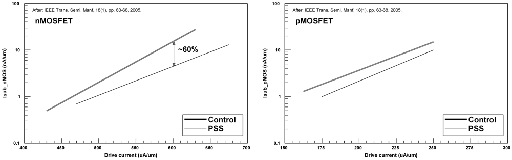
- Luo, Y.; Nayak, D.K. Enhancement of CMOS performance by process-induced stress. IEEE Trans. Semi. Manf. 2005, 18, 63–68. [Google Scholar] [CrossRef]
- Ge, C.-H.; Lin, C.-C.; Ko, C.-H.; Huang, C.-C.; Huang, Y.-C.; Chan, B.-W.; Perng, B.-C.; Sheu, C.-C.; Tsai, P.-Y.; Yao, L.-G.; et al. Process-Strained Si (PSS) CMOS Technology Featuring 3D Strain Engineering. In Proceedings of the IEEE International Electron Devices Meeting (IEDM ’03), Washington, DC, USA, 8–10 December 2003; pp. 371–374.
- Wang, T.-J.; Ko, C.-H.; Chang, C.-J.; Wu, S.-L.; Kuan, T.-M.; Lee, W.-C. The effects of mechanical uniaxial stress on junction leakage in nanoscale CMOSFETs. IEEE Trans. Electron Device 2008, 55, 572–577. [Google Scholar]
- Ban, Y.; Pan, D.Z. Compact Modeling and Robust Layout Optimization for Contacts in Deep Sub-wavelength Lithography. In Proceedings of the Design Automation Conference (DAC), Anaheim, CA, USA, 13–18 July 2010.
- Chakraborty, A.; Shi, S.X.; Pan, D.Z. Layout Level Timing Optimization by Leveraging Active Area Dependent Mobility of Strained-Silicon Devices. In Proceedings of the Design, Automation & Test Europe (DATE), Munich, Germany, 10–14 March 2008.
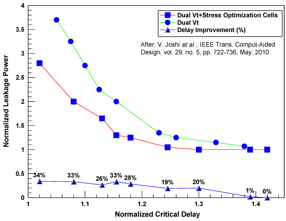
- Joshi, V.; Cline, B.; Sylvester, D.; Blaauw, D.; Agarwal, K. Mechanical stress aware optimization for leakage power reduction. IEEE Trans. Comput. Aided Des. 2010, 29, 722–736. [Google Scholar]
- Venkatraman, R.; Castagnetti, R.; Kobozeva, O.; Duan, F.L.; Kamath, A.; Sabbagh, S.T.; Vilchis-Cruz, M.A.; Jhy Liaw, J.; You, J.-C.; Ramesh, S. The design, analysis, and development of highly manufacturable 6-T SRAM bitcells for SoC application. IEEE Trans. Electron Device 2005, 52, 218–226. [Google Scholar] [CrossRef]
- Zhang, K.; Bhattacharya, U.; Chen, Z.; Hamzaoglu, F.; Murray, D.; Vallepalli, N.; Wang, Y.; Zheng, B.; Bohr, M. SRAM design on 65-nm CMOS technology with dynamic sleep transistor for leakage reduction. IEEE J. Solid State Circ. 2005, 40, 895–901. [Google Scholar]
- Smayling, M.; Axelrad, V. Simulation-Based Lithography Optimization for Logic Circuits at 22 nm and Below. In Proceedings of the International Conference on Simulation of SemiconductorProcesses and DevicesSISPAD ’09, San Diego, CA, USA, 9–11 September 2009; pp. 1–4.
- Amelifrad, B.; Fallah, F.; Pedram, M. Leakage minimization of SRAM cells in a dual-Vt and dual-Tox technology. IEEE Trans. Very Large Scale Integr. (VLSI) Syst. 2008, 16, 851–860. [Google Scholar] [CrossRef]
- Sill, F.; You, J.; Timmermann, D. Design of Mixed Gates for Leakage Reduction. In Proceedings of the 17th ACM Great Lakes Symposium on VLSI, New York, NY, USA, 11–13 March 2007.
- Yang, H.S.; Wong, R.; Hasumi, R.; Gao, Y.; Kim, N.S.; Lee, D.H.; Badrudduza, S.; Nair, D.; Ostermayr, M.; Kang, H.; et al. Scaling of 32 nm Low Power SRAM with High-k Metal Gate. In Proceedings of the IEEE International Electron Devices Meeting (IEDM 2008), San Francisco, CA, USA, 15–17 December 2008; pp. 233–236.
- Narendra, S.G. Challenges, Design Choices in nanoscale CMOS. ACM J. Emerg. Technol. Comput. Syst. 2005, 1, 7–49. [Google Scholar] [CrossRef]
- Valentian, A.; Beigne, E. Automatic gate biasing of an SCCMOS power switch achieving maximum leakage reduction and lowering leakage current variability. IEEE J. Solid State Circ. 2008, 43, 1688–1698. [Google Scholar] [CrossRef]
- Paul, A.C.; Agarwal, A.; Roy, K. Low-power design techniques for scaled technologies. Integration 2006, 39, 64–89. [Google Scholar]
- Rahman, H.; Chakrabarti, C. A leakage estimation and reduction technique for scaled CMOS logic circuits considering gate-leakage. In Proceedings of the International Symposium on Circuits and Systems, Vancouver, Canada, 23–26 May 2004; pp. 297–300.
- Lee, D.; Zhai, B.; Blaauw, D.; Sylvester, D. Ultra Low-Power Electronics and Design; Macii, E., Ed.; Kluwer Academic Publishers: New York, NY, USA, 2004. [Google Scholar]
- Chang, M.-C.; Chang, C.-S.; Chao, C.-P.; Goto, K.-I.; Ieong, M.; Lu, L.-C.; Diaz, C.H. Transistor- and circuit-design optimization for low-power CMOS. IEEE Trans. Electron Device 2008, 55, 84–95. [Google Scholar] [CrossRef]
- Razavipiur, G.; Afazali-Kusha, A.; Pedram, M. Design and analysis of two low-power SRAM cell structures. IEEE Trans. Very Large Scale Integr. (VLSI) Syst. 2009, 17, 1551–1555. [Google Scholar] [CrossRef]
- Elakkumanan, P.; Narasimhan, A.; Sridhar, R. NC-SRAM—A low-leakage memory circuit for ultra deep submicron designs. In Proceedings of the IEEE International SOC (Systems-on-Chip) Conference, Rochester, NY, USA, 17–20 September2003; pp. 3–6.
- Chuang, C.-T.; Mukhopadhyay, S.; Kim, J.-J.; Kim, K.; Rao, R. High-performance SRAM in nanoscale CMOS: Design challenges and techniques. In Proceedings of the IEEE International Workshop on Memory TechnologyDesign and Testing, Taipei, Taiwan, 3–5 December 2007; pp. 4–12.
© 2012 by the authors; licensee MDPI, Basel, Switzerland. This article is an open-access article distributed under the terms and conditions of the Creative Commons Attribution license (http://creativecommons.org/licenses/by/3.0/).
Share and Cite
Shauly, E.N. CMOS Leakage and Power Reduction in Transistors and Circuits: Process and Layout Considerations. J. Low Power Electron. Appl. 2012, 2, 1-29. https://doi.org/10.3390/jlpea2010001
Shauly EN. CMOS Leakage and Power Reduction in Transistors and Circuits: Process and Layout Considerations. Journal of Low Power Electronics and Applications. 2012; 2(1):1-29. https://doi.org/10.3390/jlpea2010001
Chicago/Turabian StyleShauly, Eitan N. 2012. "CMOS Leakage and Power Reduction in Transistors and Circuits: Process and Layout Considerations" Journal of Low Power Electronics and Applications 2, no. 1: 1-29. https://doi.org/10.3390/jlpea2010001
APA StyleShauly, E. N. (2012). CMOS Leakage and Power Reduction in Transistors and Circuits: Process and Layout Considerations. Journal of Low Power Electronics and Applications, 2(1), 1-29. https://doi.org/10.3390/jlpea2010001