Article

RF/mm-Wave Frequency Doublers in CMOS Technology

Dipartimento di Ingegneria Elettrica Elettronica e Informatica (DIEEI), University of Catania, 95125 Catania, Italy
*
Author to whom correspondence should be addressed.
J. Low Power Electron. Appl. 2026, 16(2), 14; https://doi.org/10.3390/jlpea16020014
Submission received: 2 February 2026 / Revised: 8 April 2026 / Accepted: 10 April 2026 / Published: 13 April 2026
(This article belongs to the Special Issue 15th Anniversary of Journal of Low Power Electronics and Applications)

Abstract

This paper provides a comprehensive analysis of active frequency doubler architectures adopted for efficient generation of millimeter-wave (mm-wave) signals. The operational principles of each topology are explained to address a thorough comparison based on essential performance metrics such as conversion gain, power efficiency, and spectral purity. The review covers several topologies from the standard push–push (PP) doubler to its power-efficient evolution, the complementary push–push (CPP) doubler. Furthermore, this paper focuses on more recent and advanced topologies, including the complementary common gate capacitive cross-coupled (CCGCCC) doubler. Finally, this work proposes and evaluates an improved version of the CCCGCC doubler, offering insights into the state of the art and future directions in mm-wave frequency multiplication.

1. Introduction

The persistent demand for higher data rates in wireless communications and radar sensing applications is driving the adoption of millimeter-wave (mm-wave) frequency bands. However, the direct generation of a stable, low-noise local oscillator (LO) signal at these frequencies presents significant challenges, especially in modern scaled, low-voltage CMOS technologies [1,2]. The performance of a high-frequency voltage-controlled oscillator (VCO) is often limited by the impact of parasitic capacitances on the LC tank, which severely degrades both the tuning range and phase noise [1,3,4].
To overcome these limitations, a widespread and effective architectural approach involves a lower-frequency VCO followed by a frequency multiplication block (e.g., 2× or 4×). This strategy relaxes the stringent design constraints on the VCO, enabling robust performance with a lower power budget. This “generate-and-multiply” technique has demonstrated high effectiveness in terms of cost, power consumption, and signal quality, often achieving superior phase-noise performance compared to direct mm-wave generation [5,6]. Consequently, frequency multipliers have become a fundamental building block in the design of modern mm-wave transceivers.
Frequency multipliers can be implemented by means of either passive [7] or active architectures [8,9]. While passive designs are often simpler, active multipliers are generally preferred when conversion gain and output power are critical, as both approaches can suffer from poor conversion efficiency, especially at low supply voltages. In recent years, a plethora of innovative active multiplier topologies have been proposed in the literature to address these challenges, each offering a different trade-off between gain, power consumption, area, and operational bandwidth. The cornerstone of active frequency doublers is the classic push–push (PP) topology. To enhance performance, variations, such as the complementary push–push (CPP) topology, have been introduced to improve conversion gain and save power by means of DC current reuse [8,9]. For higher multiplication factors, such as 4×, a common technique is to cascade two doubler stages [10,11,12]. Unfortunately, cascaded doublers are affected by increased silicon area and signal losses due to interconnects or coupling transformers [13,14]. A common drawback across many CMOS multiplier designs remains the low efficiency and the requirement for a high-voltage input drive from the preceding VCO [15].
This paper presents an overview of state-of-the-art active frequency doubler topologies in CMOS technology. We classify and analyze various circuit architectures, focusing on the main techniques used to overcome the inherent challenges of mm-wave frequency generation. This paper compares key performance metrics to provide a clear overview of the current landscape.
This paper is organized as follows. Section 2 reviews the fundamental principles of frequency multiplication and defines the key metrics for fair performance evaluation. Section 3 describes the most significant state-of-the-art CMOS frequency doublers, along with a novel topology, which is proposed herein for the first time. A comparative analysis of the presented doublers is carried out in Section 4 by using a 28 nm bulk CMOS technology, with the aim of highlighting the pros and cons of each topology. Finally, Section 5 concludes this paper by summarizing key trends and highlighting the main comparison outcome.

2. Key Metrics for Performance Evaluation of Frequency Doublers

The fundamental principle of frequency multiplication is based on a proper application of transistor non-linearities. In a linear system, all current and voltage signals have the same frequency content. To generate new frequencies, a circuit must exhibit a non-linear transfer function. When a pure sinusoidal input signal is applied to such a circuit, the non-linear characteristics distort the waveform, inherently creating a series of harmonics—integer multiples of the input frequency. Therefore, the core of a doubler’s design lies in exploiting the non-linear behavior of its components, such as the transconductance of a CMOS transistor, to efficiently generate the desired harmonic. A frequency-selective network, typically a resonant tank or a band-pass filter, follows the frequency generation stage and extracts the desired tone (e.g., the second harmonic for a doubler) while suppressing the original fundamental tone and all other unwanted spectral components. To evaluate the effectiveness of a doubler, the most significant parameter is the conversion gain (CG). This figure of merit quantifies the ratio of the radio frequency (RF) power (or voltage) at the desired output frequency to the RF power (or voltage) supplied at the input. For active doublers, which include amplifying devices, this ratio is close to unity and is expressed as a gain in decibels. Conversely, in passive doublers, there is a higher power loss. Moreover, energy efficiency is fundamental, especially in power-constrained applications. This is measured by the power efficiency (η), which provides a more complete picture by relating the output-generated RF power to the DC power consumed by the circuit, while also accounting for the input drive power. Another equally important factor is the “quality” of the output signal. An ideal doubler would produce a single, clean tone at the target frequency. Actually, residual components of the input signal and other undesired harmonics are still present at the output. A key parameter used to evaluate this spectral purity is the frequency 2 rejection (F2rej). This metric specifically quantifies the suppression of a prominent unwanted harmonic—such as the fundamental (fin) or third harmonic (3fin)—relative to the power of the desired second harmonic output. Expressed in dBc (decibels relative to the carrier), F2rej is a direct measure of the circuit’s spectral integrity. The signal quality is also defined by its noise performance. The multiplication process inherently degrades the phase noise of the input signal by a theoretical factor of 20 · l o g 10 N , where N is the multiplication factor. Any other noise source of the doubler is added to this theoretical floor phase noise. Finally, the practical utility of a doubler is defined by its frequency bandwidth. This refers to the range of input frequencies over which the circuit can maintain its specified performance, for instance, keeping its conversion gain within a 3 dB variation. A wide operational bandwidth is a crucial feature for wideband systems, but it essentially depends on the type of filtering network (i.e., the LC network used as a resonance load) and will not be analyzed in detail in this paper, which mainly focuses on circuit topology review. Since the input and output matching networks are not within the scope of this frequency doubler comparison, the operating bandwidth, which is strictly dependent on their implementation, will not be considered as a figure of merit in this work. All of the above-reported metrics provide a comprehensive framework for analyzing, comparing, and designing frequency multipliers for modern high-frequency applications.

3. CMOS Frequency Doubler Topology

Several active frequency doubler architectures have been developed to achieve efficient mm-wave signal generation. They are described and compared through their operational principles and performance across key metrics like conversion gain, power efficiency, and spectral purity. Among the most adopted and innovative doubler topologies, this paper deals with the most representative ones. Specifically, the following subsections detail the standard PP doubler, its power-efficient evolution, namely, the CPP doubler, and the more recent complementary common gate capacitive cross-coupled (CCG) with an improved version proposed herein.

3.1. Standard Push–Push (PP) Doubler

The standard push–push doubler schematic is shown in Figure 1b. It is a cornerstone architecture in frequency doubler design [14]. Its operation relies on a differential stage, typically based on NMOS devices. The input signals applied to the gate are 180 degrees out of phase (Vin+ and Vin−), but the drains of the two transistors are connected to a common output node. Typically, transformer coupling is exploited to couple the doubler with the VCO, while the center-tap easily provides the biasing voltage, VBias, to the PP transistor pair, as shown in Figure 1a.
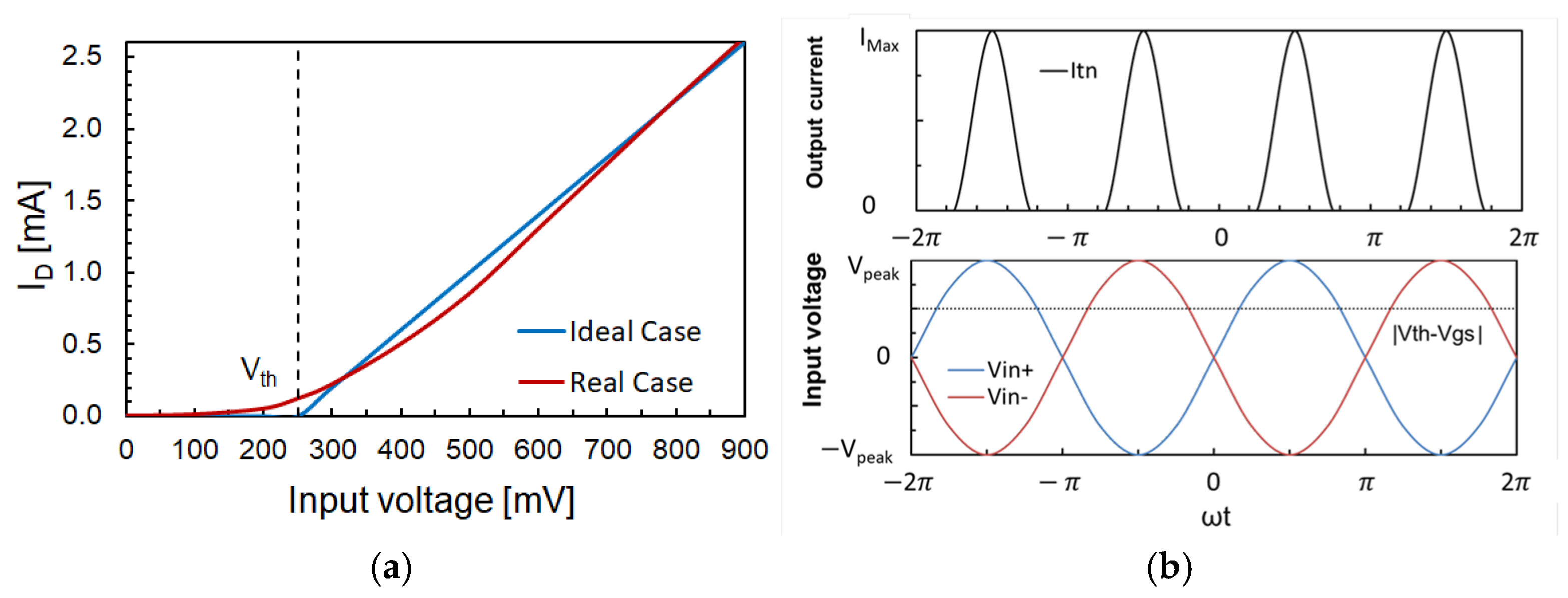
During operation, each transistor is biased to conduct for only half of the input cycle. Thanks to proper biasing and differential driving, transistors conduct on alternate half-cycles of the input waveform. Therefore, the drain currents contain a rich spectrum of harmonics of the input frequency, fin [16,17]. At the common output node, the fundamental frequency components and all odd harmonics from the two branches are out of phase and thus cancel each other out. Conversely, even harmonics, including the desired second harmonic at 2fin, are in phase and add constructively. This inherent cancellation of the fundamental provides excellent spectral purity without requiring extensive filtering, which is a significant advantage. However, the standard push–push topology has some drawbacks. Its conversion gain is upper-bounded since it heavily relies on the transconductance of the transistors. A more significant drawback is its poor power efficiency, which is due to the lack of a current-sharing mechanism. The frequency bandwidth of a PP doubler is mostly determined by its load, ZL, that is generally implemented by means of a resonant LC network, which must be carefully designed to produce a high impedance at 2fin, while shorting the other harmonics. At the heart of this circuit is the NMOS transistor. Its behavior is first approximated using a simple yet effective piecewise linear model, as shown in Figure 2a. This model treats the transistor as a voltage-controlled switch. Below a certain threshold voltage, Vth, the transistor is “off” and no current flows. Once the gate-source voltage, VGS, surpasses this threshold, the transistor turns “on,” and the drain current, i D n , begins to flow, increasing linearly with the gate voltage [9].
In its active (saturation) region, this relationship is given by (1):
i D n = 0 g m ( v i n + V G V t h )           p e r   v i n + V G < V t h p e r   v i n + V G > V t h
where g m represents the transistor transconductance, a parameter indicating how effectively the input voltage is converted into an output current. The term ( v i n + V G ) is the total voltage at the transistor’s gate, composed of the AC input signal ( v i n ) and a DC bias voltage ( V G ). Consequently, when a sinusoidal AC signal, expressed as v i n = A   c o s ω t , is applied to the gate, the transistor only conducts for a fraction of each cycle. Specifically, it turns on only when the total gate voltage is high enough to overcome the threshold voltage, V t h . This period of activity is defined by the conduction angle, θ . It essentially defines a “window” within the input cycle during which current can flow.
θ = 2 c o s 1 V t h V G A
The complete circuit shown in Figure 1b adopts a pair of transistors that work in a complementary way. One transistor handles the positive phase of the input signal, while the other handles the negative phase. This arrangement produces two streams of current pulses, i D n 1 and i D n 2 , which are 180 degrees out of phase with each other. The total output current, i T n , is simply the sum of these two streams: i T n = i D n 1 + i D n 2 . This combination is visually depicted in Figure 2b, which shows how the gaps are filled in, resulting in a pulsating current that flows on both halves of the input cycle. This is the definition of full-wave rectification. The resulting waveform, i T n , is periodic but far from a simple sinusoid. To understand its frequency components, the Fourier series in (3) can be used:
i T n t = g m A a 0 2 + k = 1 a k cos k ω i n t
where
a 0 = 2 π sin θ 2 θ sin θ 2
a k = 2 π s i n k + 1 θ 2 k + 1 + s i n k 1 θ 2 k 1 2 k cos θ 2 sin k θ 2
Equation (3) breaks down the complex current waveform into its fundamental building components: a DC component ( a 0 ) that represents the DC power generated by the circuit and depends directly on the conduction angle θ , and an infinite sum of cosine waves (harmonics) at even integer multiples of the input angular frequency ω i n . The coefficient, a k , with the even integer k, determine the strength of each harmonic. The most significant finding is that the fundamental frequency component ( k = 1 ) and all other odd harmonics, ( k = 3 ,   5 ,   7 ,   ), are completely canceled out. This is a key characteristic of a balanced full-wave rectifier and is highly desirable, as it removes the original input frequency from the output. The only AC components remaining in the output are the even harmonics. The most dominant of these is the second harmonic ( k = 2 ), whose amplitude a 2 is given by (5). Higher-order even harmonics ( k = 4 ,   6 ,   ) also exist, but their amplitudes decrease rapidly, and they are typically removed by a simple low-pass (LC) filter at the circuit’s output.
In summary, the analysis demonstrates how this transistor-based circuit transforms a pure AC sinusoidal input into a multifaceted output current. By leveraging a full-wave rectification topology, the circuit effectively suppresses the original input frequency and generates a strong second harmonic component at twice the input angular frequency ( 2 ω i n ), making the circuit an efficient frequency doubler.

3.2. Complementary Push–Push (CPP) Doubler

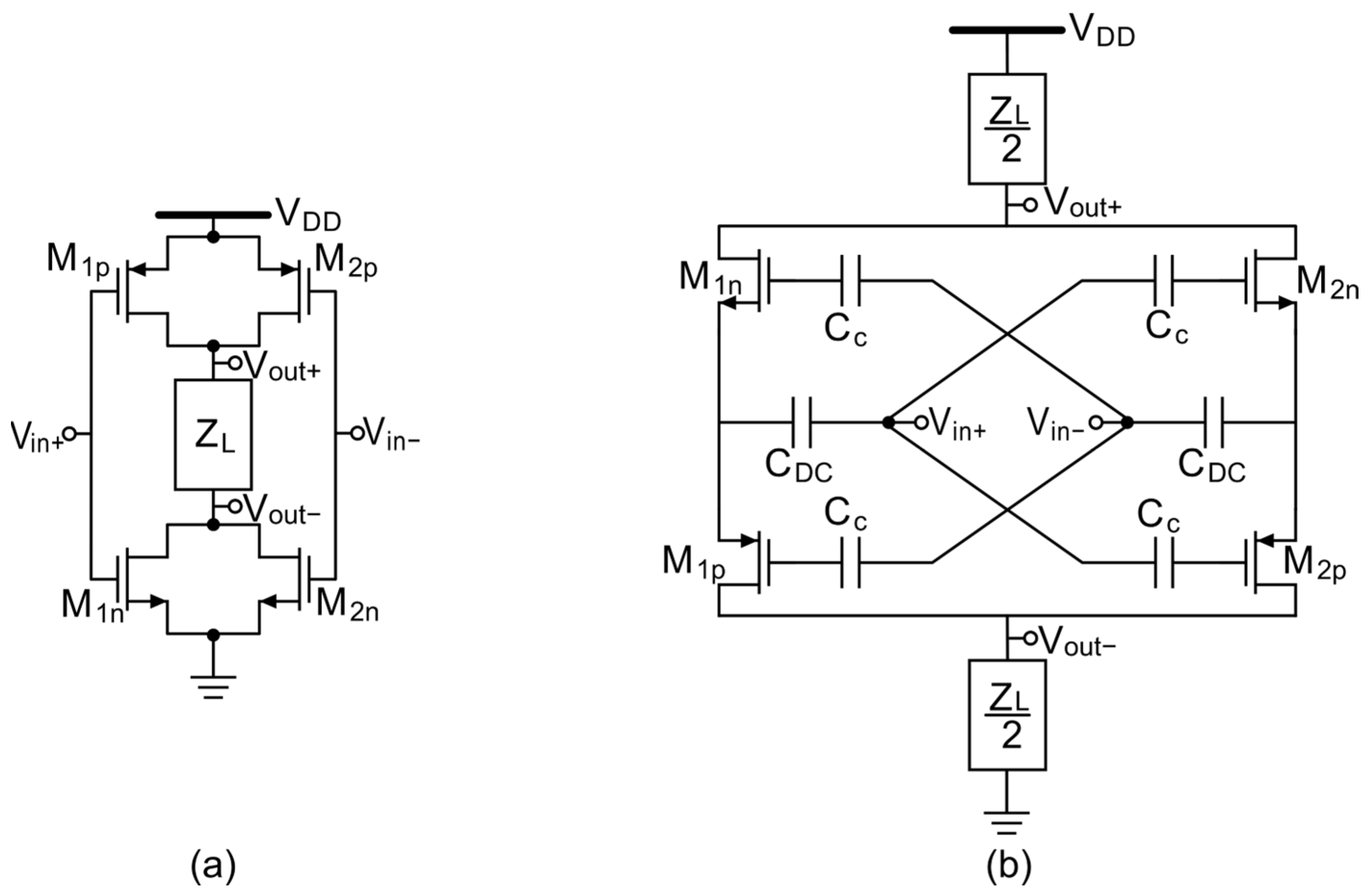
The complementary push–push doubler shown in Figure 3a was introduced to address the efficiency limitations of the standard topology. It adds a second, complementary doubler on top of the PP cell [9,18]. Indeed, the structure consists of a standard NMOS-based push–push doubler, with a second PMOS push–push doubler stacked above it. This arrangement allows both the NMOS and PMOS stages to share the same DC current path. This power-efficient technique, known as current reuse, is the key to this topology’s high performance. The differential input signal drives both the NMOS and PMOS pairs, causing them to generate the second harmonic in phase. The differential input signal is applied to the gates of both transistors. The principle of harmonic generation remains similar: the NMOS and PMOS devices conduct on opposite phases of the input signal, and their outputs are combined. At the drain node, even harmonics add constructively, while the fundamental and odd harmonics cancel. The crucial advantage here is a dramatic improvement in the power efficiency of the doubler.
Specifically, by reusing DC bias +current, the complementary topology can produce nearly double the output voltage swing for the same amount of DC current compared to the standard PP design, significantly boosting the overall power efficiency. This enhancement often translates to a higher conversion gain, as well. The improved efficiency makes this topology highly suitable for low-power applications where battery life is critical [8,9]. In terms of spectral purity, it retains the excellent fundamental rejection characteristic of the push–push configuration.
The main trade-off is an increased design complexity, as the NMOS and PMOS devices must be carefully sized and biased to ensure symmetrical operation, which can be challenging due to differences in mobility and threshold voltages. The frequency bandwidth remains largely dependent on the output matching network.

3.3. Complementary Common Gate Capacitive Cross-Coupled (CCGCCC) Doubler

A more recent and advanced architecture is the complementary common gate capacitive cross-coupled (CCGCCC) doubler [18], whose simplified schematic is shown in Figure 3b. This topology also employs a complementary NMOS/PMOS pair for current reuse, but it reconfigures the input stage significantly. Instead of a common source (CS) configuration, it uses a common gate (CG) structure. The input signal is applied to the source terminals, and the gates are AC-coupled and biased at a specific DC voltage. The “cross-coupling” is achieved through capacitors connecting the source of one transistor to the gate of the other in a feedback arrangement [18,19]. This configuration provides several distinct advantages. The CG input offers a low input impedance, which can simplify the input matching process. The capacitive cross-coupling creates a mechanism that increases the effective input voltage by two times, improving the effective second harmonic transconductance ( k 2 ) of the transistors. This   k 2 -boosting effect leads to a substantially higher conversion gain compared to the previous topologies, even at lower input drive levels and lower DC power consumption. Consequently, the power efficiency of the CCGCCC doubler is exceptionally high, making it a leading candidate for high-performance, low-power mm-wave systems. The complementary structure ensures strong fundamental and odd harmonic suppression, resulting in excellent spectral purity. The primary challenge in this topology lies in managing chip area due to the presence of two different resonant networks instead of one, as in previously complementary solutions.
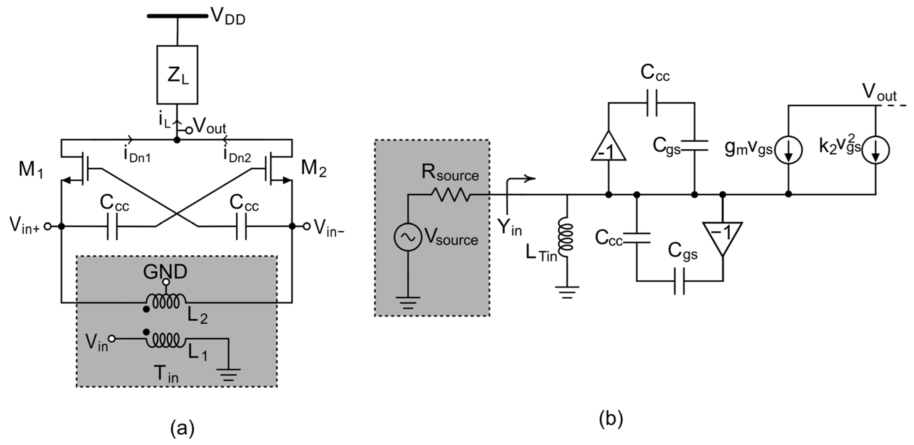
For a better understanding of the CCGCCC architecture [18], a simplified analysis of the circuit’s behavior is useful. Let us consider the NMOS side of the complementary doubler, including the input balun (L1L2), which is used for single-ended-to-differential conversion and input matching, as shown in Figure 4a. To maximize the generation of the second harmonic and thus the conversion gain, the transistors are biased in the moderate inversion region, with a gate-source voltage, v g s , close to the threshold voltage, V th :
I o u t = I D C + g m v g s +     k 2 v g s 2 +   +
  k 2 = 1 2 μ n C o x W L 1 1 + θ v g s V th 3
where C o x , μ n , and W / L are the oxide capacitance per unit of area, the electron mobility, and the transistor form factor.
The simplified half-circuit model in Figure 4b can be used to evaluate both the input impedance and the conversion gain. The input impedance, Z i n , can be analyzed using admittance ( Y ) and impedance ( Z ) matrix parameters. Under the simplifying condition that the coupling and cross-coupling capacitances are much larger than the intrinsic gate-source capacitance, C g s , ( C C > C C C >> C g s ), and considering the Miller effect on C g s , which increases the total input capacitance, the input admittance Y 11 can be calculated as:
Y 11 g m + 2 j ω 2 C g s +   1 / j ω L T i n g m   @   ω r e s
where L T i n is the inductance of the input balun and ω r e s is the angular resonance frequency of the input network. Consequently, Z i n is simply the reciprocal of Y 11 :
Z i n = 1 Y 11 1 g m   @   ω r e s
Referring to the full NMOS-side schematic, the fundamental frequency cancellation mechanism is critical to the circuit’s spectral purity. Due to the differential nature of the cross-coupling, the gate-source voltages of the transistor pair have opposite polarities (i.e., v g s 1 = v g s 2 ). This ensures that the first-order transconductance components at the fundamental frequency cancel each other out at the output node. Conversely, the second harmonic components, generated by k 2 , are in phase and sum together, doubling their total contribution. The overall current delivered to the load, i L , is the sum of the currents i D n 1 and i D n 2 , as represented in Figure 4a:
i L = 2 I D C + 8 k 2 γ 2 v i n 2 +
where γ represents the voltage partition coefficient at the input node, defined as:
γ = 1 1 + Y i n   ( R s o u r c e )
Using this framework, the conversion gain of the NMOS-side doubler (CG2×N) for an input signal v i n = A   c o s ω t can be calculated. The second harmonic output voltage, v o u t , 2 ω ,   and power, P o u t , 2 ω ,   are given by:
v o u t , 2 ω = 4 k 2 N γ 2 Z L A 2
P o u t , 2 ω = 1 2 v o u t , 2 ω 2 R e { Z L = 8 ( k 2 N γ 2 Z L A 2 ) 2 R e { Z L
Finally, the voltage conversion gain for the full complementary doubler can be found by combining the contributions of both the NMOS and PMOS stages, which further enhances the overall gain of the CPP architecture by four times:
C G 2 = C G 2 × N +   C G 2 × P = 4 k 2 N + k 2 P γ 2 Z L A
Although this architecture is highly optimized from a performance perspective, its main design challenge concerns the total silicon area. In fact, the implementation requires two separate inductors, each with an inductance of ZL/2, which inherently leads to greater layout complexity and silicon consumption compared to a single ZL inductor. This effect is particularly relevant in CMOS and BiCMOS technologies, where the integrated inductor is not limited to the metal spiral alone. To operate properly, without degrading the performance of the surrounding circuitry through noise coupling or substrate parasitics, each inductor must be surrounded by dedicated guard rings and keep-out zones imposed by layout design rules check (DRC) for reliability and isolation [9]. When two inductors are used, these containment structures are effectively duplicated, and additional minimum-spacing constraints must be respected between them, further increasing the occupied area. Moreover, each common gate transistor pair requires its own resonant load (i.e., ZL/2). This is in contrast with the CPP topology, which relies on a single inductor and can therefore achieve a significantly more compact layout footprint.

3.4. Complementary Cross-Coupled Common Gate (CCCG) Doubler

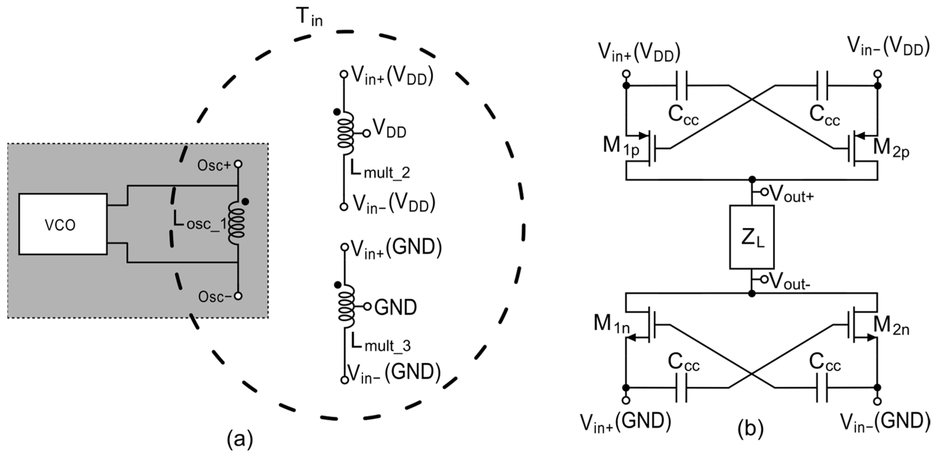
The complementary cross-coupled common gate topology is here proposed to overcome the drawbacks of the CCGCCC doubler. A simple yet effective input source-to-doubler RF coupling/biasing network uses a three-coil transformer, as shown in Figure 5a. The simplified schematic of the CCCG is depicted in Figure 5b. It exploits the same frequency multiplication mechanism described in Section 3.3 for the CCCGCC doubler [18,19], but adopts only one resonant load, thus reducing the required silicon area [20], as will be explained in the following. In order to complementarily exploit the mechanisms of the cross-coupled common gate, it was necessary to bias the input signal, v i n , with two different voltages: ground for the NMOS transistors and voltage supply, V D D , for the PMOS transistors [18]. This was made possible by using the three-winding input balun of Figure 5a. Winding LOSC_1 forms a crucial part of the oscillator’s resonant LC tank, which enables the generation of the signal at the target frequency. Windings Lmult_2 and Lmult_3 are dedicated to biasing and impedance matching for the PMOS and NMOS sides of the circuit, respectively. The CCCG analysis is similar to that of the CCGCCC doubler and, therefore, it is not repeated here to avoid useless redundancy.
As far as silicon area is concerned, the CCCG doubler is more efficient than the CCCGCC doubler, since it uses only one resonant load, (i.e., ZL in Figure 5), and hence one inductor, instead of two resonant loads (i.e., ZL/2 in Figure 3), and hence two inductors. The area advantage can be easily demonstrated by using the well-known modified Wheeler formula [21], comparing the silicon area required by a single-turn inductor (e.g., of 150 pH) with respect to two single-turn inductors (e.g., of 75 pH each). An overall silicon footprint reduction of approximately 20% is calculated for the CCCG doubler. Moreover, nanometer CMOS technologies require a keep-out zone and a guard ring structure around the inductor coil [22,23,24], which introduce a significant area overhead. It can account for up to 70% of the total footprint for a 75 pH inductor. It is evident that the CCCG doubler, employing a dual-inductor topology, is double-penalized. Finally, integrating a single inductive load makes simpler routing, which minimizes capacitive parasitics, increasing the self-resonance frequency (SRF), and improving the quality factor.
It is worth noting that, despite its three-winding topology, the adopted balun occupies almost the same area as a traditional two-winding transformer or a single inductor that would have been required anyway in the oscillator block driving the doubler [16]. Therefore, this approach maximizes silicon area efficiency, allowing it to retain the advantages of the previously discussed topologies, such as the current reuse and the conversion gain boosting of CPP and CCGCCC, respectively, within a chip size comparable to that of standard PP or CPP doublers.

4. Comparative Performance Analysis of Frequency Doublers

A performance comparison of previously discussed frequency doublers has been carried out with the aim of highlighting the pros and cons of each topology. A 28 nm bulk CMOS technology provided by TSMC was used for the comparison. This technology features a 9-metal back-end-of-line (BEOL) with a 3.5 µm ultrathick metal (M9) top layer plus a thick alucap layer (AP) of 2.8 µm. The thick top metal layers are suited to implement high-quality mm-wave inductive components. Moreover, the adopted CMOS process provides low-voltage-threshold (LVT) 0.9 V CMOS transistors that are well suited for low-power/high-frequency operation.
The topologies presented in Section 3 were used to design four different 30-to-60-GHz frequency doublers, enabling a metric-by-metric comparison under identical technological and electrical conditions. The comparison focuses on four key performance indicators: conversion gain, power consumption, power efficiency, and second harmonic rejection, evaluated as a function of the input-voltage amplitude at 30 GHz.
To guarantee a fair and consistent evaluation of the frequency doublers under comparison, the main design parameters have been set, as reported in Table 1. As far as the output network is concerned, the resonant load, ZL, is implemented by means of a 150 pH inductor lumped model with a quality factor, Q, as high as 15 at 60 GHz, thus producing an equivalent load impedance ZL = ω QL ≈ 850 Ω at 60 GHz. As a reference, integrated transformers implemented in the same CMOS process demonstrate primary coil inductances of approximately 150 pH, with Q higher than 20 at 60 GHz [25]. The use of an equivalent integrated inductor model rather than an actual component is a deliberate choice aimed at preserving a fair and architecture-centric comparison. By minimizing layout-dependent parasitic effects, the analysis remains focused on the intrinsic efficiency, harmonic generation, and scalability of the proposed frequency doubler topologies. Finally, it is worth noting that this study focuses on the analysis of the doubler core, but it does not consider the input matching network. Indeed, since each architecture inherently exhibits a different input impedance, topology-specific matching networks are required, which would add external design variables, such as impedance-dependent losses, and could hide the intrinsic performance of the doubler cores.
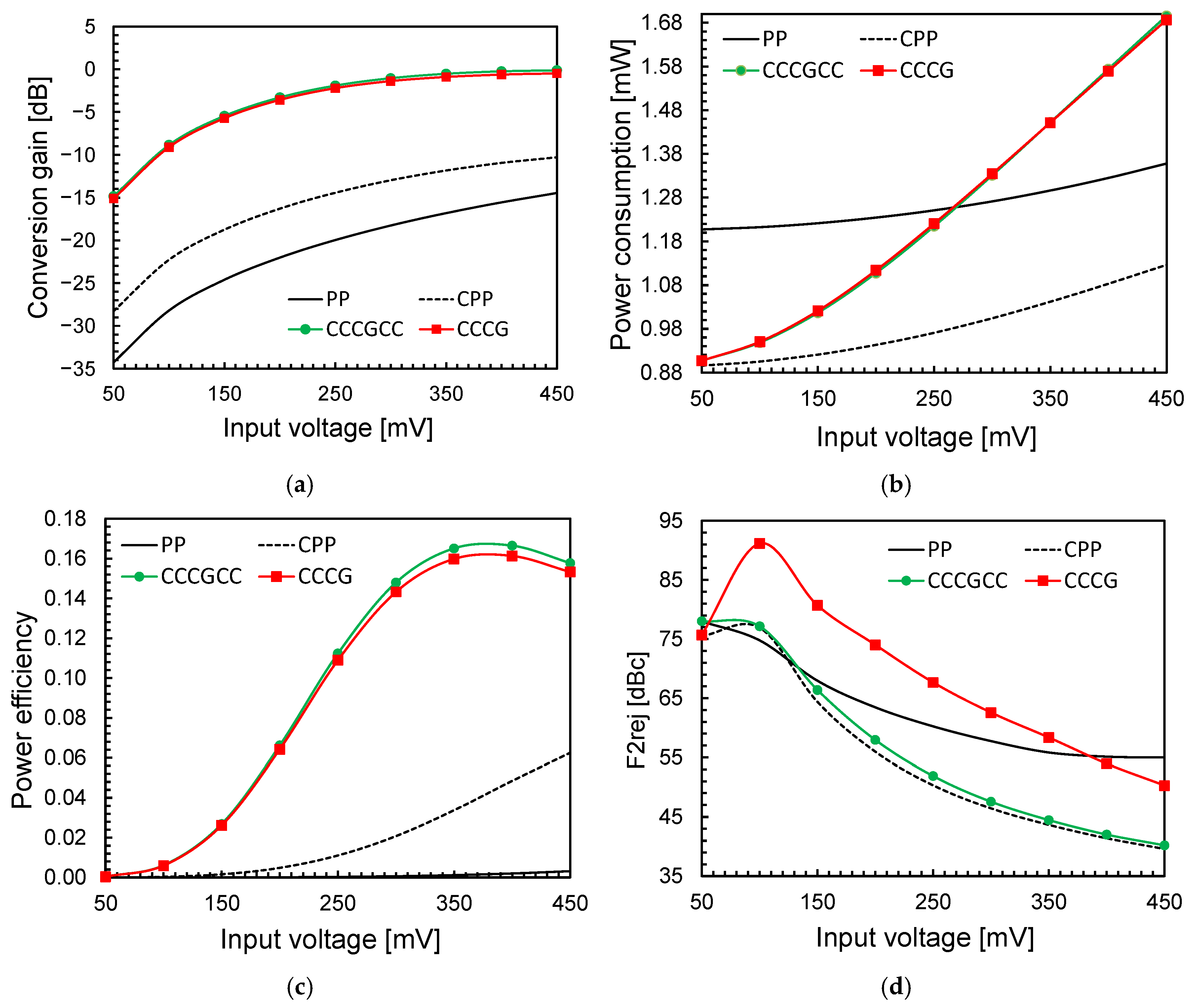
Moving to an actual performance comparison of the four frequency doubler topologies provided a clear landscape of the main design trade-offs. The main results of the doubler analysis are summarized in Figure 6 as a function of the input voltage (i.e., the peak voltage at 30 GHz). In terms of the conversion gain, as shown in Figure 6a, the CCGCCC and CCCG topologies are undisputed leaders, employing an efficient mechanism to boost transconductance. Indeed, the standard PP and CPP variants achieve considerably lower conversion gain values. In terms of power consumption, referring to Figure 6b, CPP exhibits the lowest value across the entire range of input voltage. However, the power consumption figure by itself is an incomplete and partial metric. To truly demonstrate the merit of a topology, the power consumed must be related to the generated output power. Therefore, the most comprehensive and meaningful metric is power efficiency ( η ), shown in Figure 6c. When considering power efficiency, the CCGCCC and CCCG doubler topologies are again often superior, as the cross-coupled mechanism provides a highly effective method for converting DC power into RF output. The CPP also demonstrates good efficiency, typically outperforming the standard PP.
Figure 6d depicts the frequency 2 rejection, F2rej, as a function of the input voltage, where higher values correspond to better suppression (i.e., the rejection of 30 GHz or 90 GHz with respect to 60 GHz). Overall, all topologies exhibit a monotonic decrease in rejection as the input voltage increases, which is expected as the devices progressively operate in deeper non-linear regions. The CPP topology (black dotted curve) shows a distinctive behavior: it achieves the highest rejection, peaking at approximately 90 dBc around 100 mV, but its performance degrades rapidly for higher input voltages. The PP doubler (black solid curve) demonstrates the most robust and predictable behavior, maintaining relatively stable rejection over a wide input-voltage range and outperforming the other architectures for input voltages above approximately 400 mV. The CCGCCC (green curve) and CCCG (red curve) exhibit very similar trends and closely track each other across the entire voltage range. Consequently, the choice of topology is application-dependent: CPP is suitable when very high second harmonic rejection is required within a narrow input-voltage window, whereas PP represents the most reliable solution for broadband operation and higher input-voltage levels.
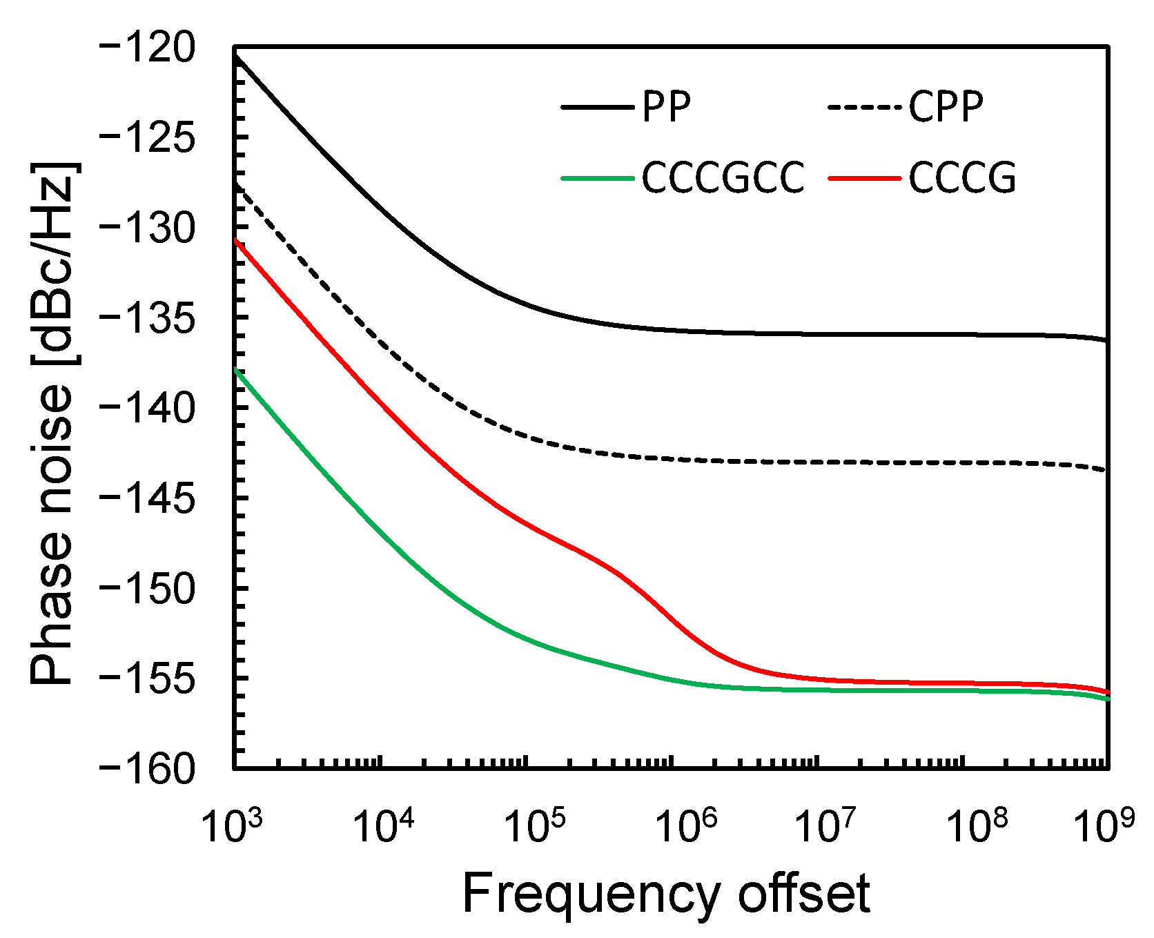
Figure 7 shows the comparison in terms of the phase noise performance. It has nearly the opposite meaning with respect to the harmonic rejection results, since lower values on the y-axis now represent a better performance. The CCGCCC topology (green curve) is the winner, exhibiting the lowest phase noise across the entire frequency offset range, making it the cleanest signal source. The other common gate design (CCCG, black curve) is the second-best performer, while CPP (red curve) ranks third. Notably, the standard PP (blue curve), which was a strong contender for harmonic rejection, shows the worst phase noise performance by a significant margin. When considering both Figure 6d and Figure 7, a clear design trade-off emerges: the standard PP doubler offers robust harmonic rejection over a wide input range but at the severe cost of high phase noise. On the other hand, the common gate topologies, especially the CCGCCC, provide excellent phase noise performance, making them ideal for applications requiring high spectral purity, though their harmonic rejection is merely adequate rather than exceptional. CPP acts as a specialist, offering first-rate harmonic rejection, but only at a low-power operating point, with poor phase noise. Therefore, the optimal choice is dictated by the primary design goal: CCCGCC and CCCG should be preferred for the lowest phase noise, while CPP should be used for low-power applications with high harmonic purity.
To evaluate the robustness of the proposed frequency doubler architectures, a comprehensive process, voltage, temperature (PVT) analysis was also carried out. The main results are summarized in Table 2, Table 3 and Table 4, followed by commentary.
A simple inspection of data in Table 2 reveals a high susceptibility of performance to process variations, delineating a counter-intuitive behavior since the fast–fast (FF) corner, instead of the slow–slow (SS) one, represents the worst-case scenario. This is due to the enhanced linearity and wider conduction angles of “fast” devices, which reduces the second harmonic generation required for an effective conversion. This phenomenon drastically penalizes the elementary topologies (i.e., PP and CPP), which exhibit an unacceptable drop of both the conversion gain and efficiency moving from SS to FF, exhibiting gain excursions exceeding 8 dB for the PP topology at 450 mV. On the other hand, more complex architectures based on cross-coupling (i.e., CCCG and CCCGCC) demonstrate superior robustness, maintaining conversion gains near or above zero and almost constant efficiency around 12–16%, even under critical conditions. Moreover, the FF corner highly degrades the fundamental rejection, F2rej, especially at lower input voltages, VIN.
The frequency doubler sensitivity to the supply voltage, VDD, can be drawn from data summarized in Table 3. An inversely proportional dependency between VDD and performance metrics is evident, depicting a scenario where energy efficiency undergoes drastic fluctuations in response to minimal bias variations (±5%). Specifically, a significant efficiency reduction is observed in CPP, CCCG, and CCCGCC topologies, as the VDD rises to 0.945 V (dropping to near-zero values), whereas surprising efficiency peaks (up to 36% for the CCCG) are recorded when the voltage is reduced to 0.855 V. This phenomenon suggests that at higher supply voltages, the transistors operate with excessive overdrive, shifting the operating point towards a region of greater linearity, which inhibits the harmonic distortion essential for frequency doubling, in addition to detrimental higher static power dissipation. Conversely, the PP doubler demonstrates excellent immunity to voltage variations, although with an overall poor performance. On the other hand, F2rej is quite constant with VDD variations for all architectures.
Finally, Table 4 shows frequency doubler performance at three different operating temperatures for increasing input peak voltage, VIN. As expected, the simulations highlight a strong inverse correlation between temperature and performance. The low-temperature condition (i.e., −40 °C) enhances performance due to higher carrier mobility and threshold voltage, which maximize conversion gain and harmonic generation, respectively. Conversely, high-temperature operation (i.e., 70 °C) produces a reduction in power efficiency. Specifically, the CPP doubler suffers a degradation of nearly 75% at 450 mV, compared to the −40 °C case (dropping from 13.4% to 3.5%), whereas the cross-coupled architectures (i.e., CCCG/CCCGCC), despite showing a significant efficiency drop (from ~23% to ~11%), demonstrate higher robustness by ensuring functionality, even under thermal stress. The conversion gain also follows this trend, reducing from positive values at −40 °C to negative values at 70 °C, highlighting that sufficient gain margin must be over-provisioned in doubler design.

5. Conclusions

The comparative analysis of the four CMOS frequency doubler architectures confirms that the optimal design choice is mainly dictated by a clear set of performance trade-offs. For those applications demanding the highest spectral purity and power efficiency, the common gate topologies are the leaders. While both the CCGCCC and the CCCG architectures deliver good results, the CCCG emerges as the best choice as it provides top-tier performance in conversion gain, efficiency, and low phase noise while consuming significantly less silicon area, which is a key advantage in cost-effective and compact-integrated circuit. In contrast, push–push architectures serve distinct roles: the standard PP is the most robust solution for consistent harmonic rejection across a wide input power range, although at the cost of poor phase noise, while the CPP acts as a highly specialized topology, offering good harmonic rejection at low-power conditions. Finally, topology selection is a strategic decision to balance contrasting specs, positioning the CCCG as the clear winner for area-efficient, high-purity signal sources, while the PP and CPP are valuable options if harmonic suppression is the overriding design target.
Next-generation wireless communications and automotive radar systems will strongly drive the evolution of mm-wave doublers. As operational frequencies push beyond 100 GHz, generating clean and stable signals becomes increasingly difficult. Consequently, area-efficient topologies, such as the proposed CCCG, will be crucial for massive MIMO and phased-array transceivers, where minimizing expensive silicon area is vital. Future research will also need to leverage deeply scaled technologies to maintain high power efficiency at low voltages, while expanding the bandwidth for multi-band operations without degrading harmonic rejection.

Author Contributions

Conceptualization, M.C. and E.R.; validation, M.C., M.E., A.B., and E.R.; formal analysis, M.C. and E.R.; methodology, M.C., M.E., and E.R.; project administration, E.R.; supervision, E.R. and A.B.; writing—original draft, M.C. and E.R.; writing—review and editing, M.C., M.E., A.B., and E.R. All authors have read and agreed to the published version of the manuscript.

Funding

This work was partially supported by the EU under the PNRR of Next Generation EU, partnership on “Telecommunications of the Future” (PE0000001—program “RESTART”).

Institutional Review Board Statement

No applicable.

Informed Consent Statement

No applicable.

Data Availability Statement

The original contributions presented in this study are included in the article. Further inquiries can be directed to the corresponding author.

Conflicts of Interest

The authors declare no conflicts of interest.

Abbreviations

The following abbreviations are used in this manuscript:
PPStandard Push–Push
CPPComplementary Push–Push
CCGCCCComplementary Common Gate Capacitive Cross-Coupled
CCCGComplementary Cross-Coupled Common Gate

References

  1. Razavi, B. Oscillators. In RF Microelectronics, 2nd ed.; Prentice-Hall: Upper Saddle River, NJ, USA, 2012; pp. 536–570. [Google Scholar]
  2. Franceschin, A.; Padovan, F.; Nonis, R.; Bevilacqua, A. On the optimal operation frequency to minimize phase noise in integrated harmonic oscillators. IEEE Trans. Circuits Syst. II Express Briefs 2018, 65, 657–661. [Google Scholar] [CrossRef] [Scilit]
  3. Monaco, E.; Pozzoni, M.; Svelto, F.; Mazzanti, A. Injection-locked CMOS frequency doublers for μ-wave and mm-wave applications. IEEE J. Solid-State Circuits 2010, 45, 1565–1574. [Google Scholar] [CrossRef] [Scilit]
  4. Iotti, L.; Mazzanti, A.; Svelto, F. Insights into phase-noise scaling in switch-coupled multi-core LC VCOs for E-band adaptive modulation links. IEEE J. Solid-State Circuits 2017, 52, 1703–1718. [Google Scholar] [CrossRef] [Scilit]
  5. Wang, S.; Chang, C.-T. K-band CMOS frequency doubler with high fundamental rejection. Electron. Lett. 2014, 50, 1211–1212. [Google Scholar] [CrossRef] [Scilit]
  6. Ellinger, F.; Jackel, H. Ultracompact SOI CMOS frequency doubler for low power applications at 26.5–28.5 GHz. IEEE Microw. Wirel. Compon. Lett. 2004, 14, 53–55. [Google Scholar] [CrossRef] [Scilit]
  7. Han, R.; Afshari, E. A high-power broadband passive terahertz frequency doubler in CMOS. IEEE Trans. Microw. Theory Tech. 2013, 61, 1150–1160. [Google Scholar] [CrossRef] [Scilit]
  8. Oh, J.; Jang, J.; Kim, C.-Y.; Hong, S. A W-band high-efficiency CMOS differential current-reused frequency doubler. IEEE Microw. Wirel. Compon. Lett. 2015, 25, 307–309. [Google Scholar] [CrossRef] [Scilit]
  9. Wu, X.; Kang, Z.; Wang, Y.; Wu, L. A 53–78 GHz complementary push–push frequency doubler with implicit dual resonance for output power combining. IEEE Trans. Circuits Syst. I 2023, 70, 1202–1213. [Google Scholar] [CrossRef] [Scilit]
  10. Saberi Ghouchani, S.; Paramesh, J. A wideband millimeter-wave frequency doubler–tripler in 0.13-μm CMOS. In 2010 IEEE Radio Frequency Integrated Circuits Symposium; IEEE: New York, NY, USA, 2010; pp. 65–68. [Google Scholar] [CrossRef] [Scilit]
  11. Vehring, S.; Ding, Y.; Scholz, P.; Gerfers, F. A 3.1-dBm E-band truly balanced frequency quadrupler in 22-nm FDSOI CMOS. IEEE Microw. Wirel. Compon. Lett. 2020, 30, 1165–1168. [Google Scholar] [CrossRef] [Scilit]
  12. Chi, T.; Papapolymerou, J.; Wang, H. A +2.3 dBm 124–158 GHz class-C frequency quadrupler with folded-transformer-based multiphase driving. In 2015 IEEE Radio Frequency Integrated Circuits Symposium; IEEE: New York, NY, USA, 2015; pp. 263–266. [Google Scholar] [CrossRef] [Scilit]
  13. Balasubramanian, S.; Vaesen, K.; Wambacq, P.; Wulff, C. A compact current-reusing 6-mW 66–92 GHz frequency quadrupler with 5% peak power-added efficiency and >36 dBc harmonic rejection in 22-nm FDSOI CMOS. IEEE Solid-State Circuits Lett. 2025, 8, 301–304. [Google Scholar] [CrossRef] [Scilit]
  14. Darban, M.S.; Ha, D.S.; Walling, J.S. Low-power mm-wave frequency quadrupler using deep class-C doublers. In 2024 19th European Microwave Integrated Circuits Conference (EuMIC); IEEE: New York, NY, USA, 2024; pp. 391–394. [Google Scholar] [CrossRef] [Scilit]
  15. Aghighi, A.; Essawy, M.; Natarajan, A.S. A frequency doubler with second harmonic feedback for wideband, efficient frequency multiplication at millimeter-wave. IEEE Trans. Microw. Theory Tech. 2024, 72, 2704–2715. [Google Scholar] [CrossRef] [Scilit]
  16. Ye, Y.; Yu, B.; Tang, A.; Drouin, B.; Gu, Q.J. A high-efficiency E-band CMOS frequency doubler with a compensated transformer-based balun for matching enhancement. IEEE Microw. Wirel. Compon. Lett. 2016, 26, 40–42. [Google Scholar] [CrossRef] [Scilit]
  17. Chen, J.; Yan, P.; Hong, W. A 50–70 GHz frequency doubler in 90 nm CMOS. In 2012 IEEE MTT-S International Microwave Workshop Series on Millimeter Wave Wireless Technology and Applications; IEEE: New York, NY, USA, 2012; pp. 1–3. [Google Scholar] [CrossRef] [Scilit]
  18. Jang, J.; Lim, H.; Kim, T.W. A CMOS complementary common-gate capacitive cross-coupled frequency doubler. IEEE Trans. Circuits Syst. II 2022, 69, 3694–3698. [Google Scholar] [CrossRef] [Scilit]
  19. Asada, H.; Matsushita, K.; Bunsen, K.; Okada, K.; Matsuzawa, A. A 60 GHz CMOS power amplifier using capacitive cross-coupling neutralization with 16% PAE. In 2011 41st European Microwave Conference; IEEE: New York, NY, USA, 2011; pp. 554–557. [Google Scholar]
  20. Spataro, S.; Salerno, N.; Papotto, G.; Ragonese, E. The effect of a metal PGS on the Q-factor of spiral inductors for RF and mm-wave applications in a 28-nm CMOS technology. Int. J. RF Microw. Comput.-Aided Eng. 2020, 30, e22245. [Google Scholar] [CrossRef] [Scilit]
  21. Mohan, S.S.; Hershenson, M.d.M.; Boyd, S.P.; Lee, T.H. Simple accurate expressions for planar spiral inductances. IEEE J. Solid-State Circuits 1999, 34, 1419–1424. [Google Scholar] [CrossRef] [Scilit]
  22. Nan, L.; Mouthaan, K.; Xiong, Y.-Z.; Shi, J.; Rustagi, S.C.; Ooi, B.-L. Impact of metal dummy fills on the performance of CMOS inductors. In 2007 IEEE Conference on Electron Devices and Solid-State Circuits; IEEE: New York, NY, USA, 2007; pp. 251–254. [Google Scholar] [CrossRef] [Scilit]
  23. Zhang, Q.; Wu, Y.; Zhao, C.; Yu, Y.; Liu, H.; Kang, K. Mechanism analysis and experiment of the effects of the guard ring on the inductors performance. IEEE Microw. Wirel. Technol. Lett. 2023, 33, 275–278. [Google Scholar] [CrossRef] [Scilit]
  24. Mariappan, S.; Rajendran, J.; Idros, N.; Manaf, A.A.; Kumar, N.; Alghaihab, A.; Nathan, A.; Yarman, B. A review of engineering techniques for CMOS on-chip inductor design and quality factor enhancement from MHz-to-GHz frequency domains. IEEE Access 2025, 13, 140473–140499. [Google Scholar] [CrossRef] [Scilit]
  25. Eghtesadi, M.; Ballo, A.; Giustolisi, G.; Pennisi, S.; Ragonese, E. A 28-nm CMOS low-power/low-voltage 60-GHz LNA for high-speed communication. Electronics 2025, 14, 2819. [Google Scholar] [CrossRef] [Scilit]
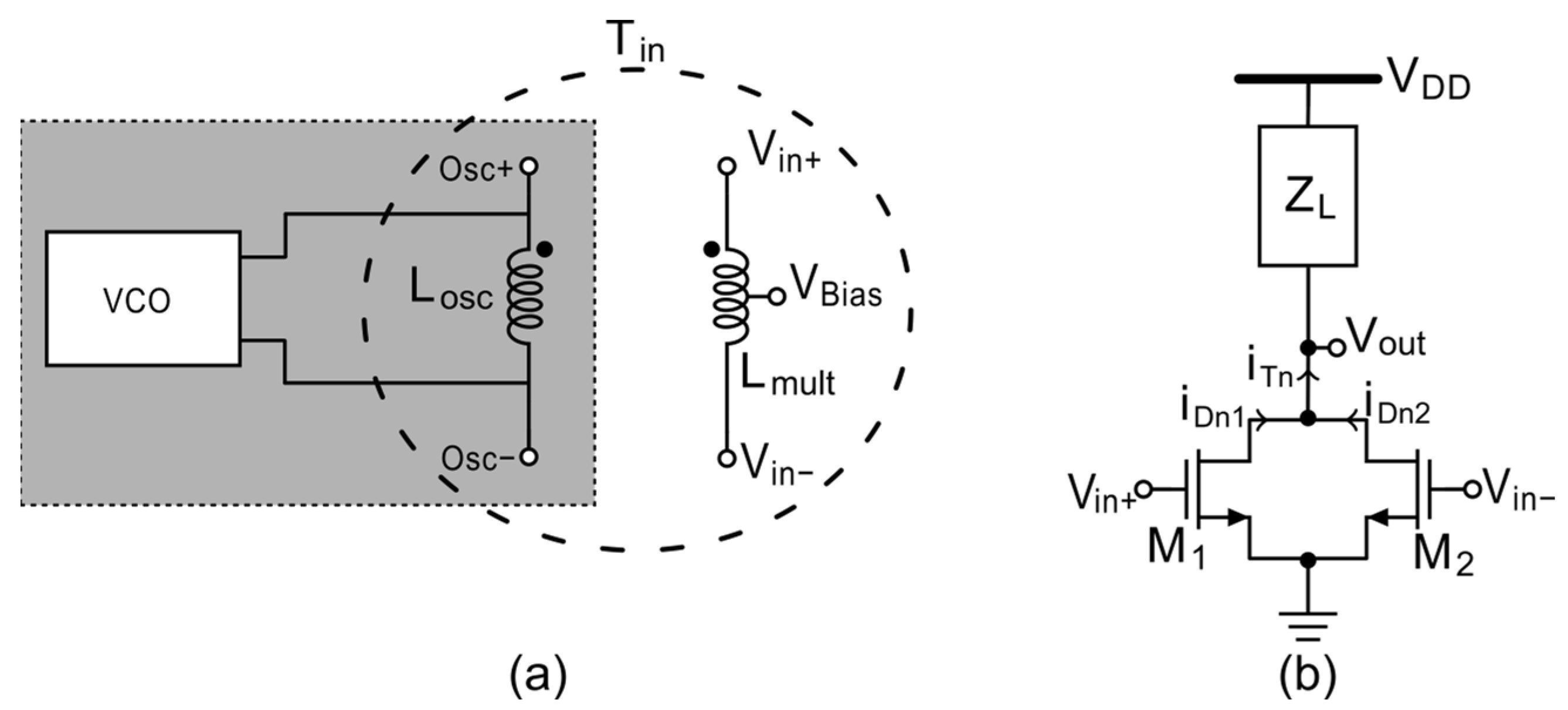
Figure 1. (a) Transformer-based coupling between the VCO and the frequency doubler; (b) standard push–push (PP) CMOS frequency doubler.
Jlpea 16 00014 g001
Figure 2. (a) Simulated I–V curve of a 300 nm NMOS transistor in a 28 nm process with VDS = 900 mV and its piecewise linear model; (b) transient waveforms of the input voltage and rectified output current for a PP doubler.
Jlpea 16 00014 g002
Figure 3. CMOS frequency doubler topologies: (a) complementary push–push (CPP) doubler; (b) complementary common gate capacitive cross-coupled (CCGCCC) doubler.
Jlpea 16 00014 g003
Figure 4. (a) NMOS-side circuit diagram of the frequency doubler; (b) half-circuit model of the cross-coupled frequency doubler.
Jlpea 16 00014 g004
Figure 5. (a) Three-coil transformer-based coupling between VCO and CCCG frequency doubler. (b) Complementary cross-coupled common gate (CCCG) doubler.
Jlpea 16 00014 g005
Figure 6. Frequency doubler comparison as a function of the peak input voltage, VIN, at 30 GHz: (a) conversion gain; (b) power consumption; (c) power efficiency (η); and (d) F2rej.
Jlpea 16 00014 g006
Figure 7. Phase noise of the four frequency doubler topologies (VIN = 250 mV at 30 GHz).
Jlpea 16 00014 g007
Table 1. Design parameters used for the frequency doubler comparison.
NMOS TransistorsPMOS TransistorsVDDZLInput Voltage, VIN
No. of terminals = 6
No. of gate fingers = 4
WLNo. of terminals = 6
No. of gate fingers = 4
WL0.9 V850 Ω @ 60 GHz50 mV–450 mV
0.6 µm30 nm1 µm30 nm
Table 2. Frequency doubler performance parameters: process variations at different VIN.
VIN [mV]CornersCG [dB]F2rej [dBc]Eff [%]
PPCPPCCGCCCCGPPCPPCCGCCCCGPPCPPCCGCCCCG
50TT−34.19−28.17−14.75−15.0180.3981.2376.1984.88000.040.04
FF−41.52−33.26−19.22−19.2650.7550.7250.8951.39000.010.01
SS−30.5−25.88−12.69−13.193.2687.1578.879.0400.010.10.1
250TT−19.89−14.32−1.84−2.1460.1567.5350.1951.760.0311.411.4611.1
FF−26.6−18.78−4.29−4.4951.6559.9359.4458.7600.295.675.55
SS−16.5−12.35−0.83−1.1470.0960.2747.5248.770.12.4516.7916.23
450TT−14.38−10.19−0.07−0.4355.0150.1839.5240.110.326.411615.54
FF−19.86−13.6−1.35−1.6544.3358.842.243.240.072.3912.812.45
SS−11.65−8.660.530.162.4247.9439.0139.310.8211.1116.7416.22
Table 3. Frequency doubler performance parameters: supply voltage, VDD, variations at different VIN.
VIN [mV]VDD [V]CG [dB]F2rej [dBc]Eff [%]
PPCPPCCGCCCCGPPCPPCCGCCCCGPPCPPCCGCCCCG
500.9−34.19−28.17−14.75−15.0180.3981.2376.1984.88000.040.04
0.855−34.02−28.47−14.69−14.4694.3580.6190.0278.52000.060.08
0.945−34.38−30.21−14.82−16.6780.1177.6877.6486.22000.020.02
2500.9−19.89−14.32−1.84−2.1460.1567.5350.1951.760.031.1411.4611.1
0.855−19.74−14.32−1.88−1.6560.5655.9149.5348.610.032.116.1818.31
0.945−20.06−16.52−1.82−3.5559.9462.5150.7151.860.030.264.633.57
4500.9−14.38−10.19−0.07−0.4355.0150.1839.5240.110.326.411615.54
0.855−14.27−9.9−0.190.0256.1546.6939.1139.70.3512.6933.5136.33
0.945−14.51−12.340.03−1.1553.7749.8939.9441.230.290.530.750.64
Table 4. Frequency doubler performance parameters: temperature variations at different VIN.
VIN [mV]Temp. (°C)CG [dB]F2rej [dBc]Eff [%]
PPCPPCCGCCCCGPPCPPCCGCCCCGPPCPPCCGCCCCG
5025−34.19−28.17−14.75−15.0180.3981.2376.1984.88000.040.04
70−35.62−30.4−16.84−17.1160.7460.6360.4461000.020.02
−40−31.4−24.34−11.06−11.3288.8686.179.4579.3500.010.120.12
25025−19.89−14.32−1.84−2.1460.1567.5350.1951.760.031.1411.4611.1
70−21.36−16.52−3.4−3.7762.3669.0353.4954.890.020.67.447.18
−40−17.09−10.80.420.2157.4460.7245.4446.810.062.9819.6319.09
45025−14.38−10.19−0.07−0.4355.0150.1839.5240.110.326.4116.0115.54
70−15.86−12.21−0.95−1.3755.8651.6641.0941.930.223.511.7111.34
−40−11.78−7.331.120.8557.5945.7337.0637.480.6213.4123.9823.38
Disclaimer/Publisher’s Note: The statements, opinions and data contained in all publications are solely those of the individual author(s) and contributor(s) and not of MDPI and/or the editor(s). MDPI and/or the editor(s) disclaim responsibility for any injury to people or property resulting from any ideas, methods, instructions or products referred to in the content.