Article

A Multiplierless Architecture for Image Convolution in Memory

Chair of Computer Architecture, Friedrich-Alexander-Universität Erlangen-Nürnberg (FAU), 91054 Erlangen, Germany
*
Author to whom correspondence should be addressed.
J. Low Power Electron. Appl. 2025, 15(4), 63; https://doi.org/10.3390/jlpea15040063
Submission received: 22 August 2025 / Revised: 14 October 2025 / Accepted: 16 October 2025 / Published: 23 October 2025
(This article belongs to the Special Issue Energy Consumption Management in Electronic Systems)

Abstract

Image convolution is a commonly required task in machine vision and Convolution Neural Networks (CNNs). Due to the large data movement required, image convolution can benefit greatly from in-memory computing. However, image convolution is very computationally intensive, requiring ( n ( k 1 ) ) 2 Inner Product (IP) computations for convolution of a n × n image with a k × k kernel. For example, for a convolution of a 224 × 224 image with a 3 × 3 kernel, 49,284 IPs need to be computed, where each IP requires nine multiplications and eight additions. This is a major hurdle for in-memory implementation because in-memory adders and multipliers are extremely slow compared to CMOS multipliers. In this work, we revive an old technique called ‘Distributed Arithmetic’ and judiciously apply it to perform image convolution in memory without area-intensive hard-wired multipliers. Distributed arithmetic performs multiplication using shift-and-add operations, and they are implemented using CMOS circuits in the periphery of ReRAM memory. Compared to Google’s TPU, our in-memory architecture requires 56× less energy while incurring 24× more latency for convolution of a 224 × 224 image with a 3 × 3 filter.

1. Introduction

Conventional computer architecture is undergoing re-engineering due to a phenomenon known as the “von Neumann bottleneck,” also referred to as the “memory wall.” This "memory wall" issue presents two primary challenges: the disparity in performance (speed) between the processor and memory and the energy consumption associated with data transfer during memory access. The energy required for data access increases exponentially as one moves through the memory hierarchy, from cache to off-chip DRAM to tertiary Non-Volatile Memory (NVM). As a result, “data movement energy” significantly outweighs “computation energy” in traditional systems that feature distinct memory and processing units [1,2,3]. This challenge is further intensified by the emergence of artificial intelligence (AI). AI hardware tasks typically necessitate the processing of substantial volumes of data, for which the von Neumann architecture proves inefficient, as it requires frequent transfers of large data sets between memory and the processor. Image processing serves as a pertinent example of such tasks, particularly in the context of machine vision and convolutional neural networks, where the process fundamentally involves convolving an image with a kernel, typically a 3 × 3 filter. Image convolution is performed on images (occupying large memory), and conventional von Neumann architecture will be inefficient for such processing if an image has to be shuttled between processor and memory.
To address this challenge, both academia and industry have been investigating alternative architectures in recent years. One such architecture is In-Memory Computing, which intentionally integrates memory and processing to enhance energy efficiency. In this approach, computation occurs within the memory array, within peripheral circuitry (such as in the sense amplifiers of the memory array), or in computational units like adders that are positioned in proximity to the memory array, a concept referred to as near-memory computing. The distinction between In-Memory Computing and Near-Memory Computing is increasingly ambiguous, as the field is rapidly evolving and numerous architectures are being proposed that facilitate sharing of computation between the memory array and the surrounding circuitry to varying degrees [3,4]. Our approach in this work can be classified as ‘In-Memory Computing’ since memory plays a key role in computing and is aided by computing units around the memory array.
Image convolution is essentially the process of superimposing a kernel/filter (usually 3 × 3) on top of an input image and calculating a weighted sum of pixel values to create a new pixel value in the output image. When the filter is superimposed on rows three to five and columns two to four of the image (Figure 1), the corresponding values are multiplied and summed. As depicted in Figure 1, for a 3 × 3 filter, this process requires nine multiplications and eight additions to calculate a single pixel in the output image. Since the image is usually large, this 3 × 3 filter has to be moved over the image many times until each pixel in the image has been covered by the filter. During convolution, the filter is usually moved by one pixel (stride = 1) and sometimes by two pixels (stride = 2) (results in a downsampled output image). Therefore, image convolution is basically computation of many Inner Products (IP), where each IP is a series of Multiply and Accumulate (MAC) operations. There are two important points to note:
(1)
Image convolution is arithmetically intensive: Assuming zero padding at the edges, a convolution of a n × n image with a 3 × 3 kernel results in n 2 IPs, where each IP requires nine multiplications and eight addition operations.
(2)
The kernel or the filter is usually fixed for a particular processing on the image. Typically, for image processing, there are standard filters like sharpen, edge detection, sobel, blur, laplacian, etc. which are applied for various tasks like smoothening, segmentation and feature extraction.
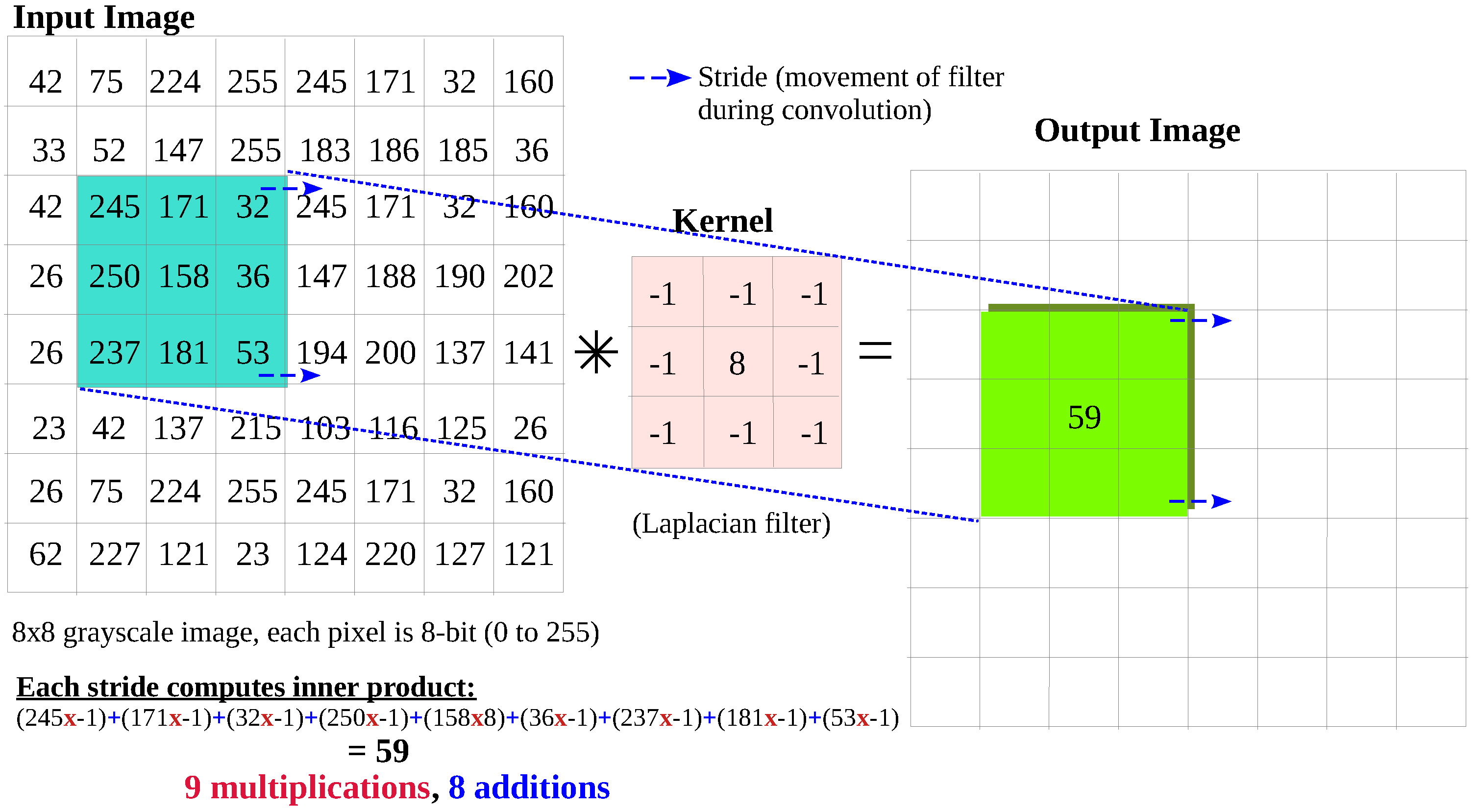
Figure 1. The 3 × 3 kernel is moved over the input image until all the pixels of the input image have been covered. Each stride computes the inner product between input pixels and kernel.
Jlpea 15 00063 g001
Multiplication is slow in CMOS-based ASIC implementation and all the more so in In-Memory implementation [5]. Therefore, it will be a challenge to perform image convolution in memory. Moreover, the input image changes, while the filters are fixed. Interestingly, an old technique in computer architecture called Distributed Arithmetic is well suited to implement such a task in memory. Distributed Arithmetic (DA) is an efficient method for calculating the Inner Product (IP) between a fixed vector and a variable vector. DA was introduced in 1974 and became a significant area of research during the 1980s and 1990s [6]. The IP of two vectors is defined as the sum of the products of their corresponding components of the two vectors, as follows:
Y = X T W = i = 1 N X i W i
where X T = [ X 1 , X 2 , , X N ] is the variable vector and W T = [ W 1 , W 2 , , W N ] is a fixed vector. For IP corresponding to each pixel in image convolution, [ W 1 , W 2 , , W N ] could represent the filter coefficients (3 × 3 kernel), which remain constant throughout the computation. Traditionally, the inner product (IP) is calculated using a Multiply and Accumulate (MAC) unit, which multiplies the weight/coefficient vector W with the input vector X and adds the results to the partial product to obtain the final sum [7]. Distributed Arithmetic (DA) represents an alternative approach to computing the same inner product Y = A T · X without the use of hard-wired multipliers. In DA, the sum of the coefficients is pre-computed and stored in memory as a look-up table. The input vector X is segmented into bits, with one bit from X 1 , X 2 , , X N being sequentially fed to the row decoder of the memory array in a bit-serial manner. This process generates the address for the memory, and the corresponding data are retrieved from there. During each iteration, the retrieved data are left-shifted (to achieve multiplication by two) and cumulatively added to compute Y. Consequently, DA facilitates a multiplierless architecture, enabling the computation of the inner product without the need for hard-wired multipliers when one of the vectors is constant.
In this work, we utilize this DA technique to design a multiplierless architecture to perform image convolution in memory. The rest of the paper is organized as follows. Section 2 presents the architecture we designed to perform image convolution in memory using DA. In Section 3, we describe how we verified our approach using an in-house tool at a higher level of abstraction. Section 4 presents the design of a sensing circuit and the computation units (adders, shifter) around the memory array to perform image convolution. After verification by transistor-level simulation, we also present the nonfunctional properties (latency, energy) of our approach to image convolution. In Section 5, we compare our approach with conventional image convolution (performed with MAC units) using Google’s TPU as an example and offer some insights into the benefits of our approach. Section 6 concludes our work.

2. Proposed Architecture for Image Convolution: Distributed Arithmetic Approach
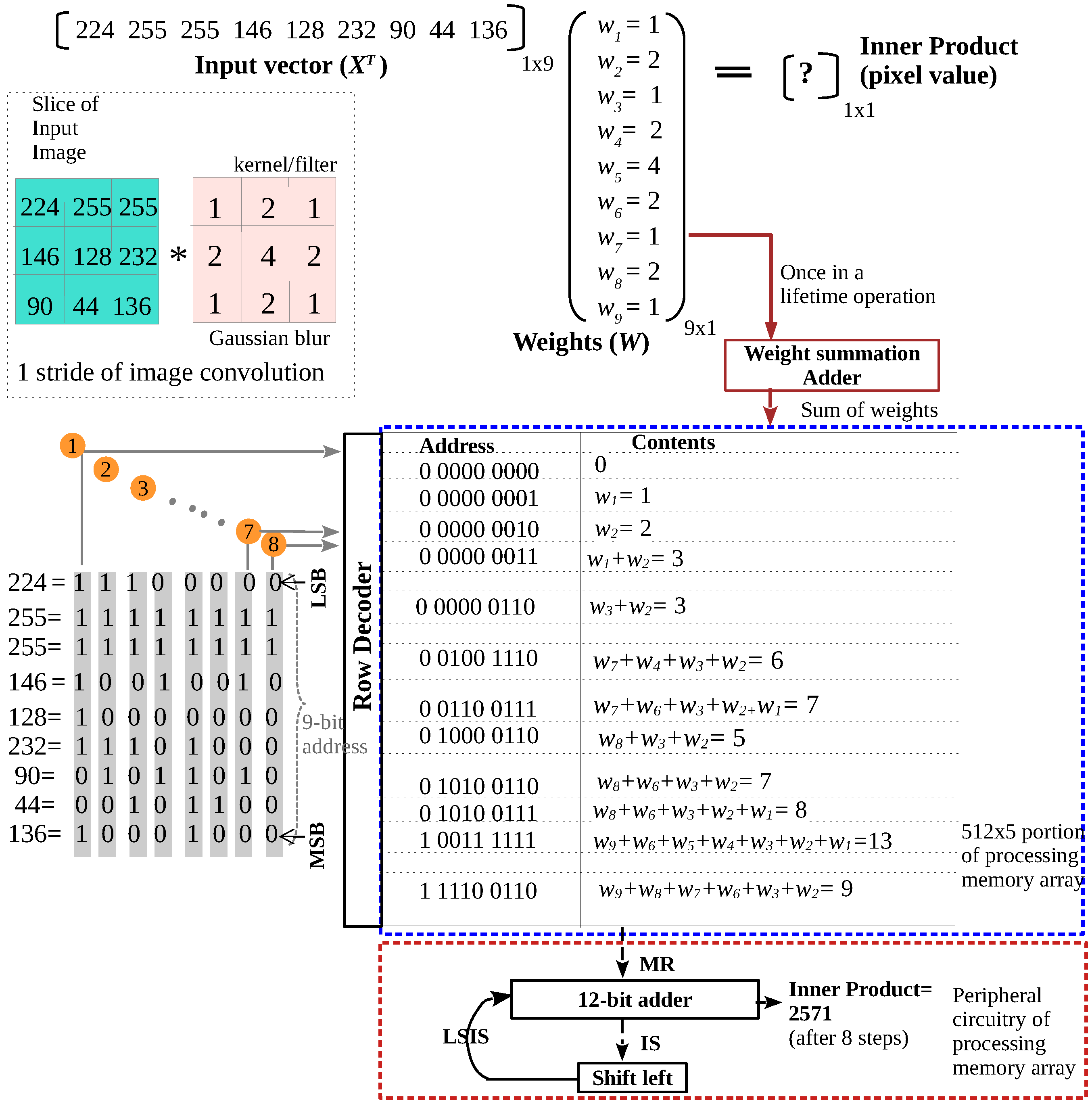
Image convolution can be viewed as series of Inner Product computations. Figure 2 depicts a slice (a stride) of the convolution between an 3 × 3 portion of an image with a 3 × 3 kernel. Here, the pixel values of the input image form the input vector X. X is the variable vector since X changes with every stride or step of the convolution process. The filter coefficients form the fixed vector W and do not change.
X T = [ 224 255 255 146 128 232 90 44 136 ] W = [ 1 2 1 2 4 2 1 2 1 ] Y = X T · W = i = 1 N X i × W i
Inner Product Y can be computed as,
Y = 224 × 1 + 255 × 2 + 255 × 1 + 146 × 2 + 128 × 4 + 232 × 2 + 90 × 1 + 44 × 2 + 136 × 1
However, as stated, using distributed arithmetic, such an IP can be achieved without hard-wired multipliers. As depicted in Figure 2, the weights are first summed to calculate all possible sums of the weights by the ‘weight summation’ adder. In this example, the maximum possible sum of the weights is 16 = ( 10000 ) 2 . For a nine-element filter, we need a 2 9 × 5 = 512 × 5 array of memory to store all possible sums of the weights. The sums of the weights are then written into the memory array in the corresponding location. For example, the data w 7 + w 4 + w 3 + w 2 = 6 are written in the location 001001110. It is important to highlight that the process of storing the weights occurs once and need not be repeated for each image that requires convolution with this filter. Therefore, while this process entails a significant investment of time and energy to write into 512 rows, it does not necessitate repetition. In Section 4, we will discuss how this effort can be effectively amortized through the use of Non-Volatile Memory.
Figure 2. A stride of Image Convolution in memory using DA.
Jlpea 15 00063 g002
By using adders in the periphery of the memory array, we can essentially compute IP in memory in a bit-serial manner. After the weights have been summed and written to the memory, the input vector is segmented, and in each step, a single bit from the set [ X 1 , X 2 , X 3 , , X 9 ] is applied to the array’s address decoder (refer to Figure 2). The decoder interprets the binary address and provides the data ‘MR’ associated with the corresponding address (’MR’ to signify Memory Readout). This value is then directed to an adder, which adds it to the previous left-shifted ‘MR’ value to obtain Y. Table 1 lists the eight steps of image convolution for the example considered in Figure 2, which has the intermediate values of M R , Intermediate sum ( I S ), and Left-shifted Intermediate Sum ( L S I S ). The MSB of [ X 1 , X 2 , , X 9 ] forms the address for step 1; the next significant bit forms the address for step 2, and so on. IP is thus attained without the use of a multiplier circuit, facilitated by DA. It is important to note that addition can, in principle, be achieved within the memory array itself, and several in-memory adders have been proposed in the recent literature [8,9,10]. However, the fastest in-memory adder requires 4 + 6 l o g ( n ) cycles to add two n-bit numbers [10], and computing IP using in-memory adders requires hundreds of memory cycles [11]. By employing CMOS adders in proximity to the memory, it is possible to execute addition operations within a single cycle, with these typically lasting only a few hundred picoseconds. Consequently, this study integrates CMOS adders at the periphery of the memory array to minimize latency and attain performance levels comparable to those of ASICs.

3. Image Convolution in Memory: Functional Verification

3.1. SystemC Tool to Evaluate In-Memory Architectures

To conduct a quick feasibility study of our in-memory convolution approach, we used a in-house crossbar (memory array) simulation tool written at a higher level of abstraction. This tool is written in SystemC and provides a modular crossbar architecture alongside different Non-Volatile Memory (NVM) cells to be used for the functional simulation of in-memory computing architectures. In this instance, values obtained from the well-known Stanford–PKU model [12] were used to interpolate the non-linear voltage-current response associated with ReRAM devices while modeling the switching of the two states based on threshold voltages. Since SystemC without the AMS-Extension is not designed to model analogue signals, voltages and currents are handled separately using floating point values at discrete time steps, leveraging SystemC’s event-based simulation for fast simulation results.
The individual cells are then organized in a crossbar, forwarding voltages within each row and accumulating currents at the columns. In order to program and read out all NVM devices, each cell is fitted with an abstract access transistor, used in this instance to disconnect the cell from its corresponding row. The data stored in the memory are read out using sense amplifiers at the columns of the crossbar, which work by comparing the current at each output to a known threshold.

3.2. Negative Filter Co-Coefficients and Adder Bit-Width

The kernel used in Figure 2 is a Gaussian blur which contains only positive integers. Figure 3 lists the prominent image filters from literature. As can be observed, many filters have negative integers; our architecture must be able to handle such filters during convolution. Negative filter coefficients can be processed by representing them in two’s complement. Hence, they can be stored in binary in the memory array and conveniently processed by our Add–Shift circuits. The bit width of the adder required is estimated as follows. If the filter has exclusively positive integers, then the sum of the positive integers is also a positive integer. In each step (Table 1), this integer (MR) is read out, added to the IS, and then left-shifted. For the Gaussian filter (W = [1 2 1 2 4 2 1 2 1]), the maximum possible MR (sum of weights) is 16 = ( 10000 2 ). Each left shift requires an extra bit (16, when left-shifted, becomes 32 and needs six bits). Since there are seven left shifts during convolution of an image that has eight-bit pixels (Table 1), we need a twelve-bit adder for the Gaussian filter.
If the filter has both positive and negative integers, then the sum of the weights can be positive or negative. Let us consider a Scharr filter W = [3 10 3 0 0 0 −3 −10 −3]). The maximum possible MR (sum of weights) is ±16. Let us analyze −16; the same analysis will hold for +16. Now we must use two’s complement representation, and we need six bits to represent MR (−16 = 110000 2 ). Each left shift requires an extra bit, as established above. Since there are seven left shifts during convolution of an image with eight-bit pixels (Table 1), we need a thirteen-bit adder for the Scharr filter. In general, the required adder bit-width is (m + 7) for convolution with eight-bit image pixels, where m is the number of bits required to represent the maximum possible sum of weights. Since there can be overflow during addition in corner cases, it is better for the adder to be wider than this minimum. Hence, in this work, we use a 16-bit adder for the convolution process.

3.3. Customization of the Tool and Functional Verification of Image Convolution in Memory

In order to use our SystemC tool for the functional verification, the address decoder, as well as the adder and shifter, were implemented in a bit-wise fashion with configurable bit widths as additional modules. Utilizing these modules enabled us to use this setup for verification that 13 bits is sufficient to obtain correct results with filters like the above-mentioned Scharr filter.
Functional verification starts by computing all coefficient sums to be stored in the processing memory. This is done on a purely functional level by using the addition built into C++ on integer values. The result is then converted into a two’s complement binary form, and the individual bits are written into the crossbar with appropriate writing voltages. Afterwards, each input X can be converted into a binary sequence as shown in Figure 2 to determine the row addresses needed in each of the following steps of the image convolution. The data stored at these addresses are then read out of the crossbar, starting with the address of the most significant bit of all inputs and proceeding to the least significant bit. During each read operation, the corresponding row is enabled, the appropriate reading voltage is applied, and the output, determined by the sense amplifiers, is added to the previous result before left shifting and continuing with the next address. This verification was performed on multiple example pixels of a reference image for the Gaussian low-pass filter, Gaussian sharpening filter, Sharr filter, Laplacian filter, and the Kirsch operator, achieving the same results obtained with traditional computation of the inner product.

4. Image Convolution in Memory: Circuit Implementation and Validation

Following verification at an abstract level, we verified our approach to image convolution by transistor-level simulation. The choice of memory technology was influenced by the need to amortize the costs associated with the energy and the time required to write the sum of the filter coefficients into memory. While volatile memory could be utilized, it would incur costs each time convolution is performed with the same filter. Consequently, we opted for Non-Volatile Memory (NVM) technology. Among Non-Volatile Memory (NVM) options, we selected Resistive RAM (ReRAM) due to its capability for low-energy programming (this places it in contrast with flash memory, which requires high-voltage WRITE circuits), as well as its technological maturity. ReRAMs are two-terminal devices, typically structured as Metal–Insulator–Metal, that are capable of storing data as resistance. When they are subjected to voltage stress, the resistance can be reversibly switched between a Low-Resistance State (LRS) and a High-Resistance State (HRS), as illustrated in Figure 4. This change in resistance results from the formation or rupture of a conductive filament within the insulator. Generally, ReRAM is constructed in a 1T–1R configuration, wherein each memory cell is equipped with an access transistor to mitigate sneak-path currents during both reading and writing processes.

4.1. Pre-Convolution Procedure

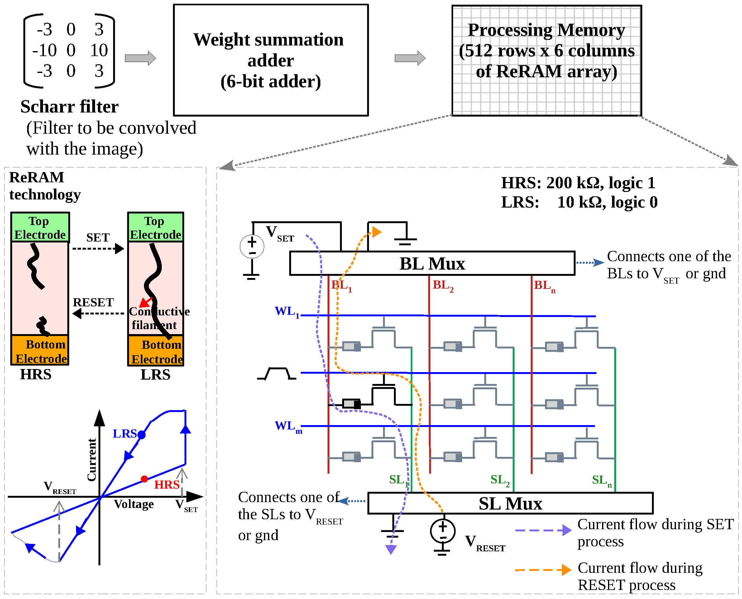
Figure 4 depicts the pre-convolution procedure to write the sum of the weights into the memory. For the Scharr filter, the filter coefficients can be positive or negative integers. The maximum coefficient is ±16; hence, six bits are needed to represent them in two’s complement form. As depicted, the filter coefficients are fed to the weight-summation adder, which is a 6-bit adder, to calculate the sum of the filter coefficients. They are then written to the 1T–1R Resistive memory. When a positive voltage V S E T is applied, the device switches from HRS to LRS. When a voltage of opposite polarity ( V R E S E T ) is applied, the devices switches back to HRS. In 1T–1R array, the SET process is accomplished by applying V S E T to the top electrode ( B L ), while the source terminal is grounded. The RESET process is accomplished by applying V R E S E T to the S L , while the top electrode ( B L ) is grounded. Denoting HRS as logic ‘1’ and LRS as logic ‘0’, (110011) can be stored as (HRS HRS LRS LRS HRS HRS) in the memory and can be written by (RESET RESET SET SET RESET RESET) operations at corresponding locations in the memory. In this manner, the sums of filter coefficients are stored in a Non-Volatile Memory. Once written, the sum of the weights remains unaltered in the processing memory and any number of images can be convolved with the filter. Since ReRAM typically has retention of 10 years, the filter weights need not be updated or modified for 10 years, and a potentially unlimited number of images can be convolved with a filter. Since we only read from the processing memory and do not write into the processing memory during convolution, ReRAM variability does not affect our architecture (note that special algorithms like Incremental Step Program Verify Algorithm (ISPVA) can be used to program the resistive memory cell with very less variability, and although it is time-consuming, it is a once-in-a-lifetime procedure). Furthermore, our in-memory convolution procedure is endurance-friendly, since we write into ReRAM once and then use it as a Read Only Memory (ROM). In principle, other NVMs like Phase Change Memory, STT-MRAM and ferroelectric memories [13] can also be used instead of ReRAM.

4.2. In-Memory Image Convolution Architecture

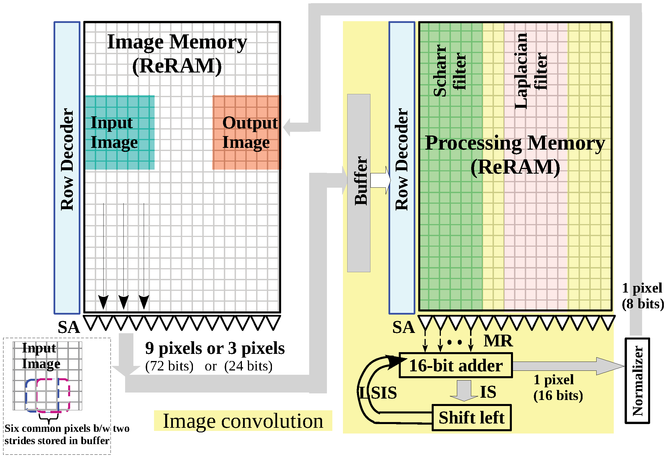
Among the computations moved to memory, image convolution benefits the most because the movement of n × n image ( n 2 pixels where each pixel can be eight bits) from memory to a dedicated processor is avoided. Figure 5 depicts the architecture we used to implement image convolution in memory. We assume the input image is available in ‘Image Memory’, which is the original location of the image. We will store the output image after convolution in this same memory. Image convolution is performed in the neighboring processing memory and its peripheral circuitry (shaded yellow). The processing memory stores the sum of the filter coefficients, as described in the previous section. Depending on the application, it may be necessary to apply different filters to the image in sequence (e.g., an image may first be subjected to denoising using a denoising filter and then to edge detection using an edge detection filter). Since storing the sum of the coefficients typically requires a 512 × 6 memory, they can be written in adjacent columns of a 512 × 512 processing memory array, as depicted in Figure 5. During convolution, only the columns corresponding to a particular filter are activated (corresponding B L ,   S L are connected to Sense Amplifiers (SA) to be read out). Hence, we do not need a separate processing array for each filter and an image can be convolved sequentially with different filters in a single processing array.
We show the movement of data during one stride of the convolution in Figure 5. In each stride, a 3 × 3 portion of the input image is convolved with the filter. This corresponds to nine pixels (72 bits) for the first stride and three pixels (24 bits) for every subsequent stride of convolution along the same row. They are read out simultaneously from the image memory by the SAs. They are then sent to a buffer, which stores them temporarily and applies them to the row decoder of processing memory. The purpose of the buffer is twofold. Firstly, the buffer is used to store the pixels that are common to consecutive strides of convolution. Secondly, the buffer is used for bit-serialization during a stride of convolution. The pixels of the input image can thus be reused between consecutive strides of convolution similar to Google’s TPU (TPU is systolic architecture to accelerate vector matrix multiplication. It consists of a 256 × 256 array of MAC units, and data needed for consecutive computation are reused instead of being fetched again from DRAM [14]). The buffer in Figure 5 stores the pixels temporarily in registers and reuses them, i.e., for two consecutive strides of the convolution along rows, six pixels are common and are stored in the buffer (Figure 5). As described in Section 2, the pixels are applied to the processing memory in a bit-serial manner. For eight-bit pixels, one bit of the nine pixels of the input image is applied to the row decoder in each memory cycle, and the buffer orchestrates this. In this manner, the buffer ensures smooth feeding of the data to the address decoder of processing memory.
The corresponding data are read out of the processing memory using the SA and applied to the 16-bit adder; this is followed by a left-shift. After eight such cycles, the result of a single stride (inner product) is available as a 16-bit output. The output pixel value is normalized (some post-processing like normalization or scaling is performed on the output image to scale the pixels of the output image to the required range; in this work, we do not perform this step since it can be performed by simple circuits at the output of the adder–shifter block) to eight-bit and then stored in the image memory. In this manner, we achieve convolution in a processing memory near the memory that stores the input image without moving the image to a dedicated processor. In the rest of the manuscript, we will focus on the image-convolution part (shaded yellow in Figure 5) and estimate the energy, latency, and hardware required for convolution operation. In this work, we restrict our analysis to 3 × 3 image filters. In principle, our architecture can be extended to larger filters (kernels) and larger filter coefficients. Our purpose in this work is to investigate the effectiveness of our distributed arithmetic approach when compared to conventional image convolution using MAC units. Having tested for smaller filters, we have extended our DA approach to larger filters (5 × 5) and larger coefficients (−128 to +127) in [15]. Moreover, this work exploits DA for vector–vector multiplication (inner product) when one of the vectors is constant, while [15] exploits DA for vector-matrix multiplication when the matrix is a constant (e.g., trained weights of a neural network during inference).

4.3. Circuit Design and Simulation Results

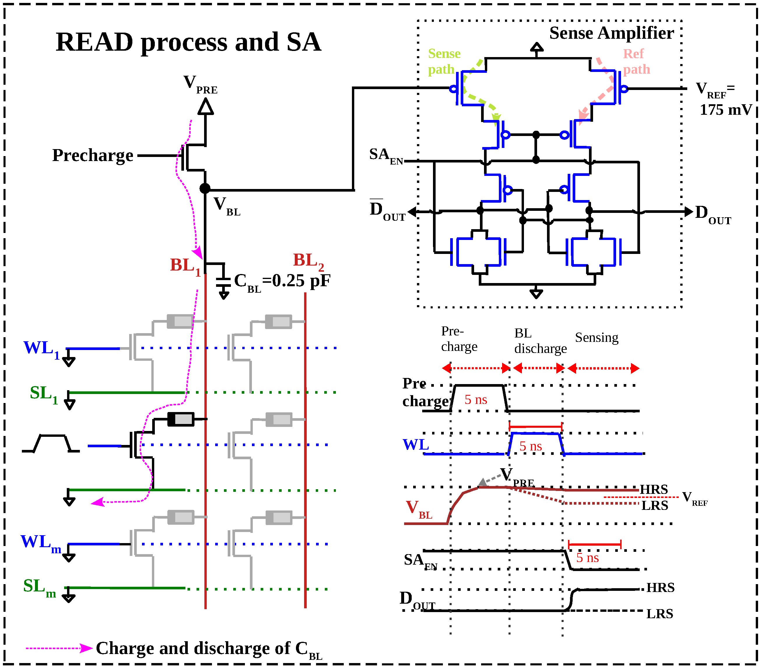
In this section, we elaborate on the hardware we designed for in-memory image convolution and present the simulation results. The processing memory we used for image convolution was a 512 × 6 1T–1R ReRAM. Given that the time and energy required for reading from the processing memory significantly impacts the efficiency of our convolution process (where a single stride necessitates eight read operations followed by addition and shifting), we have optimized our sense amplifier for enhanced reading efficiency. In general, voltage or current-mode sensing can be used. We used voltage-mode sensing because it is energy-efficient and requires a compact SA [16]. This voltage-mode sensing technique, originally presented for ReRAM in [17], is based on pre-charging and -discharging the column line (Bit Line, B L ). After discharging, the bit line voltage V B L is compared with a reference voltage V R E F to sense the state of the cell (Figure 6). The NMOS transistor above B L 1 is used to pre-charge B L 1 (bit line parasitic capacitance C B L ) to a specific voltage V P R E . We assumed the bit line capacitance of our memory array to be 250 fF, which is the reported B L capacitance for a similar memory array fabricated in a 130 nm process. B L parasitic capacitance is the sum of substrate capacitance (metal-wire-to-substrate), lateral coupling capacitance (between two metal wires) and a small fringe capacitance. Since it is hard to calculate this accurately at layout-level, we assumed the reported B L capacitance of similar structures [18,19]. After ‘Pre-charge’, the W L of the cell to be sensed is activated, and C B L , which was pre-charged to V P R E , starts to discharge in accordance with the resistance/state of the cell. If the cell is in the High-Resistance State (HRS), the discharge rate is slow and V B L V P R E . If the cell is in the Low-Resistance State (LRS), the rate of discharge is faster and V B L is much below V P R E . At the end of the B L discharge phase, the W L is deactivated and hence no more discharge is possible. The V B L is now stable and can be sensed by comparing it with a reference voltage, V R E F , using a Sense Amplifier (SA). The SA we used is adapted from the comparator proposed by T. Kobayashi et al. [20] to sense small differences between V B L and V R E F .
For IHP’s ReRAM technology, HRS is 200 kΩ and LRS is 10 kΩ. The B L was pre-charged for 5 ns and discharged for 5 ns, as depicted in Figure 6. V B L is discharged to 275 mV and 75 mV for HRS and LRS, respectively. So, a V R E F of 175 mV can be used to sense HRS as logic HIGH and LRS as logic LOW. The sensing phase was 5 ns, making the total READ latency 15 ns. The energy consumed during READ is calculated as follows. During the pre-charge and discharge phases, the energy spent in charging and discharging the B L capacitance is ascertained by integrating the current through the pre-charge transistor and the ReRAM cell, respectively.
E P r e c h a r e / D i s c h a r g e = V P R E × 0 t p r e c h a r g e I p r e c h a r g e . d t + V P R E × 0 t d i s c h a r g e I d i s c h a r g e . d t
This was found to be 29 fJ from simulations. The sensing energy (energy dissipated in CMOS comparator) was found by integrating the current drawn from V D D during sensing
E S e n s i n g = V D D × 0 t s e n s e I D D . d t
The sensing energy was found to be 6 fJ. Hence, the total READ energy is 35 fJ/bit (average of the energy to read HRS and LRS).
Figure 7 depicts the circuit we used to verify a single stride of convolution and is a detailed version of Figure 5. Two strings of D-flip-flops are used to implement the READ–Add–Shift cycle. The outputs of the six SAs are connected to the first string of D-flip-flops. The second string of D-flip-flops is connected to the output of the 16-bit adder, and they implement the left shift by one bit. We hardwired the outputs of these D-flip-flops to implement left-shift i.e., S 15 , S 14 S 1 is fed to b 16 , b 15 b 2 . Notice that the ‘D’ input of the flip-flop connected to b 1 is grounded and implements the ‘0’ injected during every left-shift. As stated, the READ latency per bit is 15 ns, and this is followed by a add cycle, which incurs another 2.5 ns. Since these eight cycles (READ followed by Add–Shift) are repeated for n 2 pixels, this latency is crucial, and we reduced it by pipelining. As the waveforms depict, ‘Pre-charge’, ‘ W L i ’ and S A E N are activated for 5 ns, and they implement the READ from processing memory. After S A E N , the A D D clock is activated for 2.5 ns, and this implements the first ADD. However, during the same period, ‘Pre-charge’ is activated to get ready for the next M R . Hence, ADD and ‘Pre-charge’ overlap and process different data. Following this second ‘Pre-charge’, W L i corresponding to the second nine-bit address is activated. The corresponding contents M R 2 are read out when S A E N is LOW; this step is then followed by a second Add–Shift.
We used a 16-bit parallel-prefix adder from [10]; this adder is fast, and the added output are available in few hundred ps. The output of the adder is fed back to the adder (through D-flip-flops) in a left-shifted manner. The LSIS is ready at the positive edge of the next A D D clock, and new M R is added with LSIS. After 122.5 ns, the inner product Y is available at the output of the adder. Using the circuit in Figure 7, we verified correct computation of the inner product for a random image patch convolved with Gaussian and Scharr filters. Hence, our in-memory convolution concept is suitable for filters with both positive and negative integers as filter co-efficients.

4.4. Performance Metrics for Single Stride of Convolution

4.4.1. Energy

In this section, we will evaluate the energy for a single stride of convolution. Each stride of convolution requires eight memory cycles. In each cycle, six bits are read ( M R ), and this is followed by an Add–Shift operation. Energy consumed by the adder/shifter circuits was calculated by integrating the current drawn from V D D during Add–Shift and multiplying it by V D D . The energy consumed by the 16-bit adder and the shifter (D-flip-flops in Figure 7) during a stride of the convolution was 445 fJ and 563 fJ, respectively. Therefore, the energy per stride is E s t r i d e = 48 × 35 fJ + 445 fJ + 563 fJ = 2.7 pJ.

4.4.2. Latency

For a single stride of convolution, READ followed by Add–Shift needs to be repeated eight times. The first memory readout M R 1 is available after 15 ns, and after that, A D D clock goes HIGH for 2.5 ns, performing the 16-bit addition (in practice, our parallel-prefix adder incurs only a few hundred ps, but we allocated 2.5 ns as a safety margin). As depicted in Figure 7, this addition happens in parallel to the next READ operation. Hence, the latency per stride is 8× the time to read out M R i plus 2.5 ns for the last addition, and Y is available after 122.5 ns. However, as depicted in Figure 7, the ( n + 1 ) th stride of convolution can start 120 ns after the start of nth convolution, and the latency of a single stride of convolution is only 120 ns (except the last stride).

4.4.3. Area

In the in-memory computing paradigm, the area requirement refers to the area occupied by the extra peripheral circuits that were added to enable convolution in memory. Since a normal memory array has SAs and decoding capability, this extra peripheral circuitry includes adders used to compute the sum of the weights, adders used to compute the inner product, and other circuits. For typical image-processing filters, the coefficients are six bits wide; therefore, we will need a six-bit adder to compute the sum of filter coefficients. Since writing into the processing memory is once-in-a-lifetime process, this can be done sequentially (it is not time-critical) using a six-bit adder. Thus, we need a six-bit adder and sixteen-bit adder–shifter for the convolution process. As depicted in Figure 5, we need a buffer to store 15 pixels (buffer stores the pixel data required for the present and the next stride and storing each pixel requires eight-bit registers) and apply them as address during convolution. Registers are constructed using D-flip-flops (24 transistors). Hence, the area of the extra peripheral circuitry required to enable convolution in memory can be roughly estimated as the area required for 4748 transistors.
A r e a = A 6 b i t a d d e r + A 16 b i t a d d e r + A D F F s + A b u f f e r = 328 + 1036 + 21 × 24 + 15 × 8 × 24 = 4748   t r a n s i s t o r s

5. Comparison with Conventional Image Convolution

5.1. Energy and Latency Estimate of Convolution in Google’s TPU

Conventional image convolution is performed by MAC units in an ASIC processor, e.g., a Tensor Processing Unit (TPU) from Google. In this section, we perform quantitative comparison of our in-memory convolution approach with Google’s TPU by estimating the energy and latency in both approaches. The energy in the conventional approach is the sum of the energy required to fetch the n × n image from memory and the energy for convolution in the MAC units. Since Google’s TPU uses a systolic architecture, the input pixels are reused during the strides of the convolution (nine pixels need not be fed to the MAC units for every stride of image convolution). Therefore, it is better to estimate the total energy for convolution of an image instead of convolution energy per stride. Considering a 224 × 224 pixel image (ImageNet standard) where each pixel is eight bits, this will require 401,408 bits to be moved from DRAM to TPU. Google’s TPU brings the data from DDR3 DRAM [14]. From [1,21], the access energy in DDR3 is 20 pJ/bit. This consists of the energy to access a row and the energy to move the data across the memory bus to the TPU. The energy to move the input image from DRAM to TPU for convolution is therefore E I m a g e M o v e m e n t = 401,408 × 20 pJ/bit = 8028 nJ (a 3 × 3 kernel is brought once from DRAM, and the energy to move it is therefore negligible compared to the energy to move the image).
TPU can perform 92 TeraOPs per second, consuming 40 W [14]. Each OP is a scalar operation and is typically a multiply or add operation. A multiply followed by an add forms a MAC. Hence, a TPU can perform 46 Tera MACs with 40 W.
E n e r g y p e r M A C = 40   W 46 × 10 12   MACs = 0.87 pJ/MAC. Each stride of image convolution will require nine such MAC operations; therefore, the computation energy per stride is E s t r i d e = 9 × 0.87 pJ = 7.83 pJ. The computation energy for convolution of a 224 × 224 image is 50,176 × 7.83 pJ= 392.8 nJ. The total convolution energy is 8421 nJ.
The access latency for DDR3 is 70 ns [21], and this is the time required to get the first bit after sending the READ command. Latency of convolution in TPU is not straightforward to estimate due to the systolic architecture, which is heavily pipelined. The MAC units are much faster (having the capability to perform 46 × 1012 MACs/s), and the latency of convolution in TPU is mainly dominated by the latency involved in bringing the input image from DRAM to TPU. Due to the pipelined architecture, the first pixel data are processed by the MAC units as they arrive from DRAM. We expect data to come 1600 × 106 bits/s (DDR3). The 401,408 bits of the input image will need 250.8 μ s. We need to add some MAC processing latency for the last pixels to enter the pipeline; this, we approximate to be 30 ns. The total latency will be ≈250.9 μ s for the entire image convolution.

5.2. Energy and Latency Estimate of Convolution Using DA

As in Google’s TPU, the input pixels can be reused in our architecture. The Buffer in Figure 5 stores the pixels temporarily in registers and reuses them. Therefore, to calculate image-movement energy, we will calculate the energy to READ 224 × 224 pixels from ReRAM. Since ReRAM is partitioned into subarrays, we will assume a 512 × 512 memory to store the input image. The energy to READ is therefore 35 fJ/bit, the same as the energy to read from processing memory. For each row, the pixel in the first column is read three times during convolution. All other pixels are read only once since the six common pixels between adjacent row strides are stored in the buffer, as depicted in Figure 5. Hence, the total number of pixels read during a single convolution is 224 × 224 + (224 × 2) = 50,624 pixels = 404,992 bits.
E I m a g e M o v e m e n t = 404,992 × 35 fJ/bit = 14.2 nJ.
Each stride of convolution consumes 2.7 pJ (Section 4.4).
E c o n v o l u t i o n (without pre-convolution cost) = 14.2 nJ + (50,176 × 2.7 pJ) = 150 nJ. To this, we must add the energy for the pre-convolution procedure. If we consider a 3 × 3 kernel, we need to write the sum of the coefficients to 2 9 = 512 rows. The typical WRITE energy in ReRAM technology is 1 pJ/bit [22], and the pre-convolution procedure consumes 512 × 6 × 1 pJ = 3 nJ. Note that this WRITE energy is a once-in-a-lifetime cost. This energy is distributed across the number of times the filter is utilized during convolution. Even when accounting for a moderate estimate of 1000 convolutions, this results in an energy cost of 3 pJ per image convolution, which is negligible in comparison to the cost associated with E c o n v o l u t i o n .
The latency of a stride of convolution is the sum of latency to read the pixels from image memory and the convolution operation in processing memory. Since only three to nine pixels are read from image memory per stride, this can be performed simultaneously, requiring 15 ns. A single stride of convolution using our pipelined procedure requires 120 ns. The pixel data required for the ( n + 1 ) th stride can be read from image memory during the nth stride and stored in the buffer. Therefore, reading the pixel data for each stride does not add to the total latency, except for the first stride.
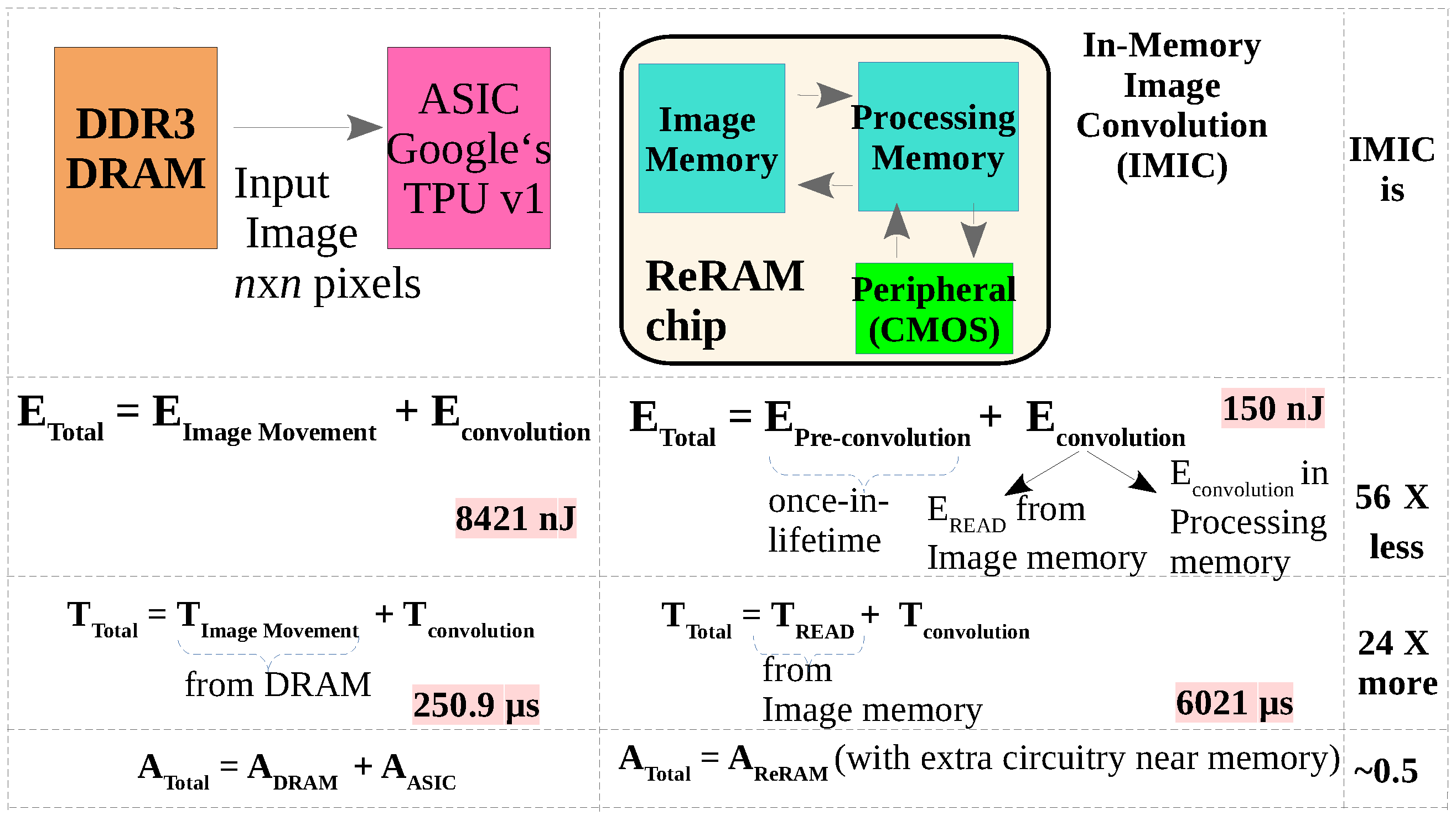
Total latency = 15 ns + 50,176 × 120 ns + 2.5 ns (last addition) = 6021 μ s. Figure 8 and Table 2 summarizes the quantitative comparison of our approach with convolution in Google’s TPU. We are able to perform convolution of a 224 × 224 image with a 3 × 3 filter with 56 times less energy and 24 times more latency compared to Google’s TPU. Note that this increased latency is the result of assuming a single processing memory array (Figure 5), and it can be reduced if a second memory array is used to perform convolution on another portion of the same image in parallel (Additionally, using a transmission gate between the B L and the SA can help in reducing latency [15]). Area comparison is not straightforward, since we augment a Non-Volatile Memory with few additional circuits to perform convolution (except the adder and shifter circuits, all other hardware like row decoders and SAs are integral parts of any memory array). We would like to emphasize that our approach requires a single chip (ReRAM with extra peripheral circuitry), while Google’s TPU needs two chips.

6. Conclusions

In this paper, we have proposed a multiplierless architecture to perform image convolution in memory. We achieve this by re-purposing a normal Non-Volatile Memory to compute IP using a distributed arithmetic technique. IP is computed with minimal alterations to the memory structure, i.e., extra adder/shift circuits to aid computation are added to the peripheral circuitry. Hence, the proposed architecture can be easily adopted by present NVM technologies, since implementing our approach will require minimal modifications to a regular memory. The sequential Add–Shift operations are optimized for latency by pipelining. Although our architecture requires 24× more time for convolution, it requires 56× less energy and does not require a separate processor to perform convolution. Hence, it is ideally suited for edge computing applications where battery power and area are limited.

Author Contributions

Conceptualization, J.R.; methodology, J.R.; software, B.S.; validation, F.Z., B.S.; formal analysis, J.R.; investigation, F.Z., B.S., J.R.; writing—original draft preparation, J.R., B.S.; writing—review and editing, J.R., F.Z.; visualization, J.R.; supervision, J.R.; project administration, J.R., D.F.; funding acquisition, D.F. All authors have read and agreed to the published version of the manuscript.

Funding

This research was performed in Bayerisches Chip-Design-Center (BCDC) funded by Bayerisches Staatsministerium für Wirtschaft, Landesentwicklung und Energie (Grant number RMF-SG20-3410-2-17-2).

Data Availability Statement

The original contributions presented in this study are included in the article. Further inquiries can be directed to the corresponding author.

Conflicts of Interest

The authors declare no conflicts of interest.

References

  1. Horowitz, M. Computing’s energy problem (and what we can do about it). In Proceedings of the 2014 IEEE International Solid-State Circuits Conference Digest of Technical Papers (ISSCC), San Francisco, CA, USA, 9–13 February 2014; pp. 10–14. [Google Scholar] [CrossRef]
  2. Mutlu, O.; Ghose, S.; Gómez-Luna, J.; Ausavarungnirun, R. Processing data where it makes sense: Enabling in-memory computation. Microprocess. Microsyst. 2019, 67, 28–41. [Google Scholar] [CrossRef]
  3. Reuben, J.; Ben-Hur, R.; Wald, N.; Talati, N.; Ali, A.H.; Gaillardon, P.E.; Kvatinsky, S. Memristive logic: A framework for evaluation and comparison. In Proceedings of the 2017 27th International Symposium on Power and Timing Modeling, Optimization and Simulation (PATMOS), Thessaloniki, Greece, 25–27 September 2017; pp. 1–8. [Google Scholar] [CrossRef]
  4. Nguyen, H.A.D.; Yu, J.; Lebdeh, M.A.; Taouil, M.; Hamdioui, S.; Catthoor, F. A Classification of Memory-Centric Computing. J. Emerg. Technol. Comput. Syst. 2020, 16, 1–26. [Google Scholar] [CrossRef]
  5. Lakshmi, V.; Reuben, J.; Pudi, V. A Novel In-Memory Wallace Tree Multiplier Architecture Using Majority Logic. IEEE Trans. Circuits Syst. I Regul. Pap. 2022, 69, 1148–1158. [Google Scholar] [CrossRef]
  6. White, S. Applications of distributed arithmetic to digital signal processing: A tutorial review. IEEE ASSP Mag. 1989, 6, 4–19. [Google Scholar] [CrossRef]
  7. Mehendale, M.; Sharma, M.; Meher, P.K. DA-Based Circuits for Inner-Product Computation. In Arithmetic Circuits for DSP Applications; John Wiley & Sons, Ltd.: Hoboken, NJ, USA, 2017; Volume 3, pp. 77–112. [Google Scholar] [CrossRef]
  8. Jha, C.K.; Mahzoon, A.; Drechsler, R. Investigating Various Adder Architectures for Digital In-Memory Computing Using MAGIC-based Memristor Design Style. In Proceedings of the 2022 IEEE International Conference on Emerging Electronics (ICEE), Bangalore, India, 11–14 December 2022; pp. 1–4. [Google Scholar] [CrossRef]
  9. Reuben, J. Design of In-Memory Parallel-Prefix Adders. J. Low Power Electron. Appl. 2021, 11, 45. [Google Scholar] [CrossRef]
  10. Reuben, J.; Pechmann, S. Accelerated Addition in Resistive RAM Array Using Parallel-Friendly Majority Gates. IEEE Trans. Very Large Scale Integr. (VLSI) Syst. 2021, 29, 1108–1121. [Google Scholar] [CrossRef]
  11. Lakshmi, V.; Pudi, V.; Reuben, J. Inner Product Computation In-Memory Using Distributed Arithmetic. IEEE Trans. Circuits Syst. I Regul. Pap. 2022, 69, 4546–4557. [Google Scholar] [CrossRef]
  12. Jiang, Z.; Wu, Y.; Yu, S.; Yang, L.; Song, K.; Karim, Z.; Wong, H.S.P. A Compact Model for Metal–Oxide Resistive Random Access Memory with Experiment Verification. IEEE Trans. Electron Devices 2016, 63, 1884–1892. [Google Scholar] [CrossRef]
  13. Jooq, M.K.Q.; Moaiyeri, M.H.; Tamersit, K. A New Design Paradigm for Auto-Nonvolatile Ternary SRAMs Using Ferroelectric CNTFETs: From Device to Array Architecture. IEEE Trans. Electron Devices 2022, 69, 6113–6120. [Google Scholar] [CrossRef]
  14. Jouppi, N.P.; Young, C.; Patil, N.; Patterson, D.; Agrawal, G.; Bajwa, R.; Bates, S.; Bhatia, S.; Boden, N.; Borchers, A.; et al. In-Datacenter Performance Analysis of a Tensor Processing Unit. SIGARCH Comput. Archit. News 2017, 45, 1–12. [Google Scholar] [CrossRef]
  15. Zeller, F.; Reuben, J.; Fey, D. Multiplier-free In-Memory Vector-Matrix Multiplication Using Distributed Arithmetic. arXiv 2025, arXiv:2510.02099. [Google Scholar] [CrossRef]
  16. Reuben, J. Resistive RAM and Peripheral Circuitry: An Integrated Circuit Perspective. 2024. Available online: https://books.google.com.au/books?id=M-gIEQAAQBAJ&printsec=frontcover&source=gbs_book_other_versions_r&redir_esc=y#v=onepage&q&f=false (accessed on 15 October 2025).
  17. Chang, M.F.; Wu, J.J.; Chien, T.F.; Liu, Y.C.; Yang, T.C.; Shen, W.C.; King, Y.C.; Lin, C.J.; Lin, K.F.; Chih, Y.D.; et al. Embedded 1Mb ReRAM in 28nm CMOS with 0.27-to-1V read using swing-sample-and-couple sense amplifier and self-boost-write-termination scheme. In Proceedings of the 2014 IEEE International Solid-State Circuits Conference Digest of Technical Papers (ISSCC), San Francisco, CA, USA, 9–13 February 2014; pp. 332–333. [Google Scholar] [CrossRef]
  18. Okuno, J.; Kunihiro, T.; Konishi, K.; Maemura, H.; Shuto, Y.; Sugaya, F.; Materano, M.; Ali, T.; Lederer, M.; Kuehnel, K.; et al. Demonstration of 1T1C FeRAM Arrays for Nonvolatile Memory Applications. In Proceedings of the 2021 20th International Workshop on Junction Technology (IWJT), Kyoto, Japan, 10–11 June 2021; pp. 1–4. [Google Scholar] [CrossRef]
  19. Okuno, J.; Kunihiro, T.; Konishi, K.; Materano, M.; Ali, T.; Kuehnel, K.; Seidel, K.; Mikolajick, T.; Schroeder, U.; Tsukamoto, M.; et al. 1T1C FeRAM Memory Array Based on Ferroelectric HZO With Capacitor Under Bitline. IEEE J. Electron Devices Soc. 2022, 10, 29–34. [Google Scholar] [CrossRef]
  20. Kobayashi, T.; Nogami, K.; Shirotori, T.; Fujimoto, Y. A current-controlled latch sense amplifier and a static power-saving input buffer for low-power architecture. IEEE J. Solid-State Circuits 1993, 28, 523–527. [Google Scholar] [CrossRef]
  21. Weis, C.; Mutaal, A.; Naji, O.; Jung, M.; Hansson, A.; Wehn, N. DRAMSpec: A High-Level DRAM Timing, Power and Area Exploration Tool. Int. J. Parallel Program. 2017, 45, 1566–1591. [Google Scholar] [CrossRef]
  22. Lanza, M.; Wong, H.S.P.; Pop, E.; Ielmini, D.; Strukov, D.; Regan, B.C.; Larcher, L.; Villena, M.A.; Yang, J.J.; Goux, L.; et al. Recommended Methods to Study Resistive Switching Devices. Adv. Electron. Mater. 2019, 5, 1800143. [Google Scholar] [CrossRef]
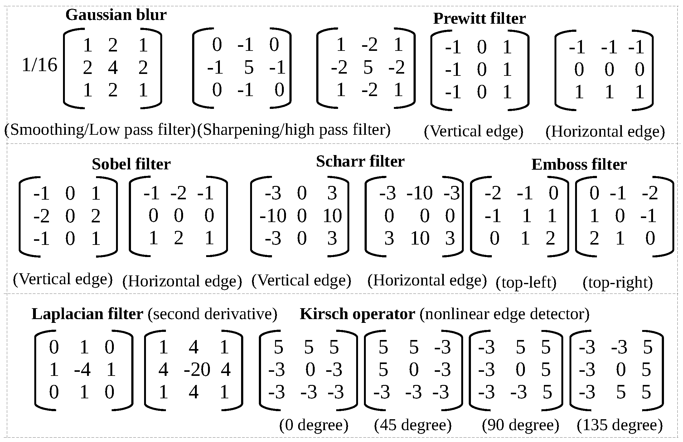
Figure 3. Typical image-processing filters from the literature; our in-memory convolution can be used to convolve an image with any of these filters.
Jlpea 15 00063 g003
Figure 4. Before convolution, the coefficients of the filter are summed and written to the processing memory, which is made of ReRAM cells.
Jlpea 15 00063 g004
Figure 5. In-Memory image-convolution architecture and the movement of data during one stride of image convolution.
Jlpea 15 00063 g005
Figure 6. READ process and Sense Amplifier. Sensing is performed in 15 ns by a sequence of ‘Pre-charge’, W L and S A E N signals, each activated for 5 ns.
Jlpea 15 00063 g006
Figure 7. Detailed circuit to implement convolution: ( a 16 a 1 ) forms the first input to the 16-bit adder and is fed with M R . ( b 16 b 1 ) is the second input of the adder and is fed with LSIS. For image convolution with standard filters (Figure 3), the filter coefficient is always six bit; hence, only six bits are read out of processing memory. The remaining 10 bits ( a 16 a 7 ) are initialized to ‘1’ if the left-most bit of M R is ‘1’ (negative number) or ‘0’ if the left-most bit of M R is ‘0’ (positive number).
Jlpea 15 00063 g007
Figure 8. Illustration of energy and latency comparison between our approach and Google’s TPU.
Jlpea 15 00063 g008
Table 1. Intermediate values during IP computation (Figure 2).
StepAddressMRISLSIS
11 0011 1111131326
20 0110 011173366
30 1010 0111874148
40 0100 11106154308
51 1110 01109317634
60 1000 011056391278
70 0100 1110612842568
80 0000 011032571
Table 2. Energy and latency comparison between our approach and Google’s TPU for convolution of a 224 × 224 image (ImageNet standard) with a 3 × 3 kernel.
ASIC (Google TPU v1)In-Memory Image ConvolutionIMIC Is
Energy8421 nJ150 nJ56× less
Latency250.9 μs6021 μs24× more
Area/Hardware256 × 256 array of Multiple-and-Accumulate (MAC) unitsTwo ReRAM arrays with peripheral circuitry of 4748 transistors
Disclaimer/Publisher’s Note: The statements, opinions and data contained in all publications are solely those of the individual author(s) and contributor(s) and not of MDPI and/or the editor(s). MDPI and/or the editor(s) disclaim responsibility for any injury to people or property resulting from any ideas, methods, instructions or products referred to in the content.