Article

A Physical Unclonable Function Based on a Differential Subthreshold PMOS Array with 9.73 × 10⁻⁴ Stabilized BER and 1.3 pJ/bit in 65 nm

by
Benjamin Zambrano
1,
Sebastiano Strangio
2,
Esteban Garzón
1,
Alessandro Catania
2,
Giuseppe Iannaccone
2 and
Marco Lanuzza
1,*
1
Department of Computer Engineering, Modeling, Electronics and Systems (DIMES), University of Calabria (UNICAL), 87036 Rende, Italy
2
Department of Information Engineering, University of Pisa, 56122 Pisa, Italy
*
Author to whom correspondence should be addressed.
J. Low Power Electron. Appl. 2025, 15(3), 53; https://doi.org/10.3390/jlpea15030053
Submission received: 8 July 2025 / Revised: 4 September 2025 / Accepted: 13 September 2025 / Published: 17 September 2025
(This article belongs to the Topic Advanced Integrated Circuit Design and Application)

Abstract

This paper introduces a physical unclonable function (PUF) based on a differential array of minimum-sized PMOS devices. Each response bit is obtained by comparing the two analog outputs of the differential array through a dynamic comparator with a trimmable offset. This offset is effectively used to mask potentially unstable response bits. To further improve PUF reliability, spatial majority voting is also implemented, resulting in a near-zero (< 3.12 × 10 9 ) bit error rate (BER) at 1.2 V and 25 ° C . Under variations in supply voltage (0.8–1.3 V) and temperature (0–75 ° C ), the native bit error rate of 3.5% is reduced to 9.73 × 10 4 after stabilization, consuming only 1.37 p J per output bit.

1. Introduction

Physical unclonable functions (PUFs) play a crucial role in hardware security by providing hard-to-clone digital fingerprints from inherent and unpredictable manufacturing variability in integrated circuits [1,2,3,4,5,6]. From a behavioral perspective, a PUF can be modeled as a hardware primitive that generates unpredictable, unique, and stable output responses (keys), useful for device authentication or data encryption.
To ensure the unpredictability (entropy) of the PUF responses, output bits can be derived by comparing analog quantities that, although nominally identical, inevitably differ due to variations in the CMOS manufacturing process. A typical approach leverages inherent differences in CMOS threshold voltage ( V th ) [4,7]. However, this method alone cannot ensure stability, as the reliability of the PUF responses can be affected by the sensitivity of the analog circuit to supply voltage and temperature fluctuations. Beyond CMOS-based designs, PUFs exploiting non-volatile memories have also been proposed [8,9,10].
Various techniques have been proposed to improve the stability of raw PUFs, at the cost of additional hardware resources and/or increased processing overhead [7]. Adding redundancy through error correction codes (ECCs) is the most common stabilization technique [11,12], but this usually leads to a significant increase in silicon area [13]. Another effective approach is spatial majority voting (SMV), which combines multiple primitive bits to generate a single, more robust response bit [14]. SMV helps to mitigate voltage- and temperature-induced instability by statistically reducing the adverse impact of bit cells with higher sensitivity to voltage and temperature (V/T) variations. Similarly, the same PUF bit can be generated multiple times and then post-processed through a temporal majority voting (TMV) scheme to counteract on-chip noise [15]. Another error-reduction strategy is the key bit preselection, where only bits likely to be stable against V/T variations are chosen, and the remaining unstable ones are masked [16]. This can be implemented directly by evaluating the PUF response bits multiple times across the applicable V/T range, or indirectly by running a “tilt” test [16] to identify the instability level of the bit cells [17,18].
In this paper, we propose a PUF based on a differential PMOS array operating in the subthreshold regime. Each response bit is obtained by comparing the two analog outputs of the differential array through a dynamic comparator with a trimmable offset. This offset is also used to preselect and mask potentially noisy response bits. Additionally, SMV is applied to further improve the PUF stability under different temperature and voltage conditions. It is worth noting that our approach is essentially different from voltage-divider [19] and SRAM-based [20] PUFs. While those schemes rely on digital or mixed-signal principles, our design is intrinsically analog in nature, exploiting voltage comparison across resistive paths rather than relying on digital state retention or simple ratio-based dividers.
The proposed PUF was fabricated using a commercial 65 nm CMOS process and was experimentally evaluated. Our architecture ensures very high integration density since only two PMOS transistors are directly involved in generating each response bit, while the additional circuitry is shared across the entire design. This resource-sharing strategy significantly reduces per-bit overhead, offering a more scalable solution compared to SRAM-based or voltage-divider PUFs, where larger device counts or per-cell resources are required. Across a supply voltage range from 0.8 V to 1.3 V and temperature variations from 0 ° C to 75 ° C , our PUF demonstrated a bit error rate (BER) of 9.73 × 10 4 , with energy consumption of 1.37 p J per bit.
The rest of this manuscript is organized as follows. Section 2 details the primitive PUF design, while Section 3 describes the test chip implemented in a 65 nm CMOS and discusses measurement results. Moreover, a comparison with prior state-of-the-art works is also reported. Finally, conclusions are drawn in Section 4.

2. The Physical Unclonable Function (PUF) Primitive

As shown in Figure 1a, the core of our PUF primitive is a differential PMOS array that generates two output voltages, V L and V R , in response to the input stimuli V R 1 V R 4 and V C 1 V C 4 . Then, a dynamic comparator with an adjustable offset produces the PUF bit response by evaluating the voltage difference between V L and V R ( Δ V LR ). The comparator offset can be finely tuned using the analog voltage signals VcalP and VcalN. Note that, during the calibration phase, the comparator inputs are provided externally.

2.1. PUF Core

As detailed in Figure 1b, the PUF core essentially consists of two arrays with four columns of four series-connected PMOS devices. The two PMOS arrays share two native transistors, N1– N2, which operate as a low-complexity voltage regulator [21] to maintain the node V X at a nearly constant value of about 500 m V . Devices D1 and D2 are diode-connected high-threshold-voltage (HVT) PMOS transistors used to decouple the two arrays.
The main source of entropy in our PUF implementation arises from the V th difference between two minimum-sized PMOS devices selected from two separate arrays. For a given address, a specific pair of PMOS transistors is selected by applying V R i = V HIGH to the i-th (where i = 1 4 ) row selection signal, while the remaining rows are driven to V LOW . At the same time, an NMOS transistor is turned on through the signals V C 1 V C 4 , thereby enabling a single PMOS stack per array. The PUF output is derived based on the voltages V L and V R , which are determined by the equivalent resistances of their respective transistor stacks. As illustrated in the inset of Figure 1b, these resistances are dominated by the resistances of the selected PMOS devices (the resistance “R” of a selected PMOS is almost four orders of magnitude larger than the resistance “r” of an unselected PMOS), with their V th directly impacting the resistance values. Charge sharing is not an issue for our design, as V L and V R are deliberately maintained to be sensitive to voltage variations to ensure a robust comparison of the resistive paths in the selected PUF columns. The parallel paths of nonselected columns are effectively suppressed, given that their NMOS transistors are off throughout the PUF primitive output bit generation. By selecting the same row and the same column in both arrays, we obtain a total of 16 unique combinations. Note that we restrict the use of the same row selection for both arrays to compare devices with similar body-to-source and source-to-drain voltages, thus minimizing the DIBL and body effects that could potentially produce unwanted bias in the extracted V th of the transistors. Additionally, limiting the selection of corresponding columns between the two arrays ensures that each transistor contributes to only one unique bit response. This choice avoids any potential correlation between the PUF bit responses. Because corresponding rows and columns are selected at a time in the two arrays, a total of four bits is enough for challenge encoding: two bits are used to select one of the four rows, and two more bits to select one of the four columns.

2.2. Comparator

Each bit of the PUF response is provided by the dynamic comparator shown in Figure 1c. This comparator consists of two stages: a floating inverter amplifier (FIA) used to minimize the impact of the input common mode [22] and an output latch with added PMOS transistors for offset calibration. The calibration process involves introducing a voltage difference V L , ext V R , ext with the required offset for the comparator and asserting signal En c (see Figure 1a). The voltage signals VcalP and VcalN are then adjusted to ensure that the comparator toggles reliably between logic ‘1’ and ‘0’.
It is worth noting that PUF cells were designed with minimum-size transistors and without mismatch-reduction techniques to maximize σ V th . While this increases variability (and thus entropy), it also leads to higher noise, especially under subthreshold bias. To address this trade-off, the offset-trimmable capability of the comparator (discussed in depth in Section 3.2) was used to implement a masking approach aimed at suppressing noisy bits and enhancing key reliability.

3. Results

3.1. Test Chip and Measurement Setup

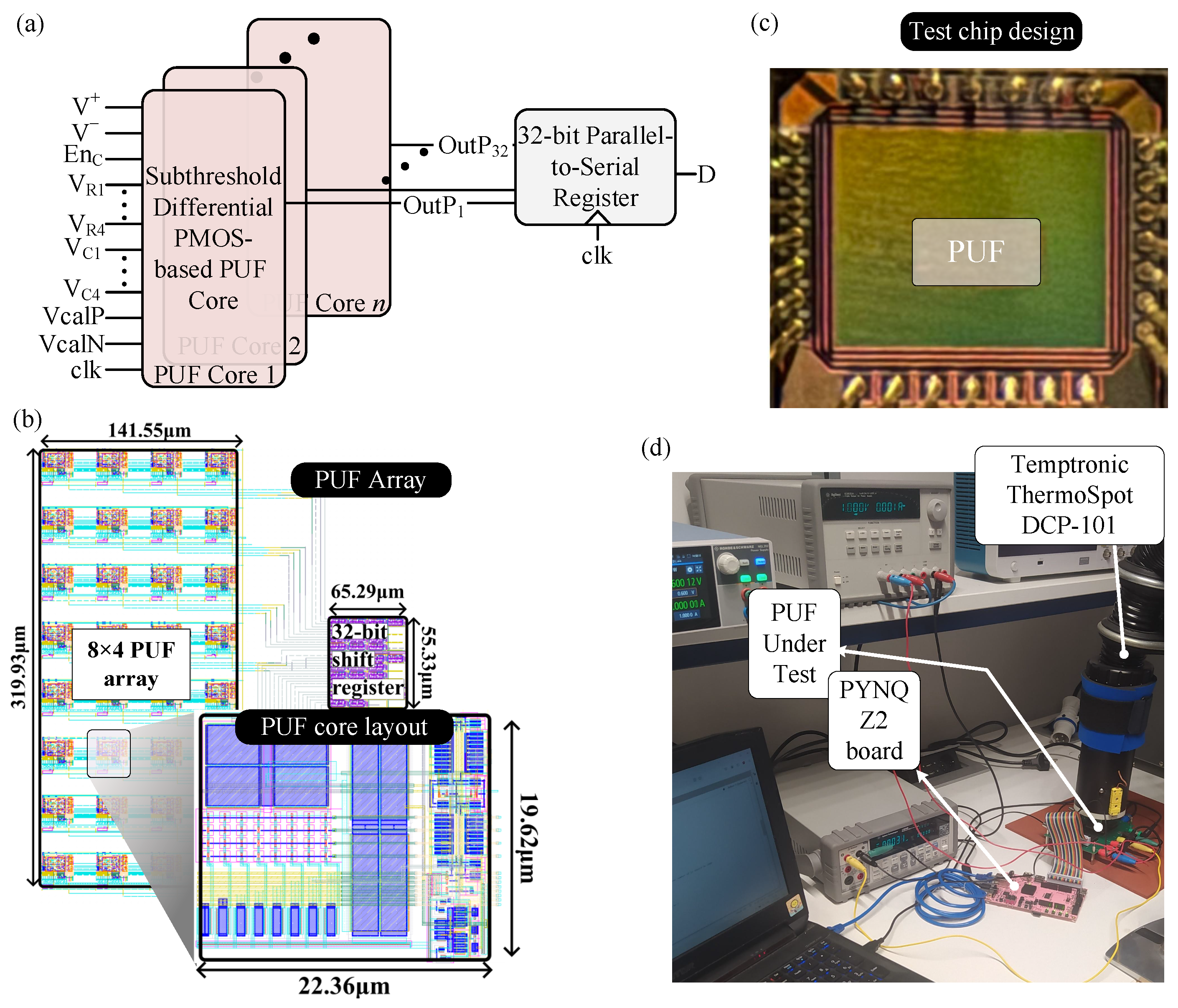
Our design was fabricated in a commercial 65 nm, 1.2 V CMOS process. Measurements were performed on ten test chips, each integrating 32 PUF primitives with a 32-bit parallel-in serial-out (PISO) shift register to store the PUF output (D), as shown in Figure 2a. The challenge size is 128 bits, structured as 32 sub-challenges of 4 bits each. Every PUF primitive receives a 4-bit sub-challenge and generates a single response bit, resulting in a 32-bit overall response. Consequently, our design supports 2 128 challenge–response pairs (CRPs). At the same time, since each PUF primitive can map its 4-bit input space into 16 uniquely selected output bits, the PUF chip encompasses a total of 32 × 16 = 512 unique response bits.
For each chip, 1000 randomly generated challenges were applied, with each challenge repeated 1000 times, yielding a total of one million response evaluations per chip. Figure 2b depicts the layout of the 8 × 4 PUF array (with magnified PUF core) and the 32-bit shift register. The area footprint of a PUF core, the full array, and the shift register are about 438.70 μ m 2 , 45,286 μ m 2 , and 3612 μ m 2 , respectively. Figure 2c,d show the test chip micrograph and measurement setup, which comprises a TUL PYNQ-Z2 board (Tul Corporation, New Taipei City, Taiwan) to extract the PUF keys and a Temptronic ThermoSpot DCP-101 (InTest Thermal Solutions, Mansfield, MA, USA) for temperature conditioning. A PUF key consists of 32 bits, where each bit corresponds to a unique physical PUF primitive.

3.2. Bit Error Rate Characterization

The capability to trim the comparator offset is leveraged to mitigate the impact of on-chip noise, which can cause instability in some output bits when Δ V L R is small. The following masking procedure is exploited to identify these noisy bits. First, a positive offset of δ   m V is externally forced to the comparator through the proper VcalP and VcalN values (as extracted during the calibration procedure described in Section 2.2). The bit-stream responses to all addresses are recorded, generating a “positive-offset” map. This process is repeated with a negative offset of − δ   m V to produce a “negative-offset” map.
Bits that show different logic values between the two maps—suggesting possible susceptibility to noise, since they are produced from Δ V L R < | offset | (voltage masking window)—are flagged as unstable. To enhance PUF robustness, such bits are masked by excluding the specific addresses that generate them. In contrast, bits that consistently exhibit the same logic value across both maps demonstrate better noise immunity, as they result from Δ V L R exceeding the specified voltage masking window. For a standard PUF operation, the comparator offset is calibrated to approach 0 m V to maximize the noise margin. This final calibration step requires fine-tuning the offset adjustment knobs (i.e., VcalP and VcalN in Figure 1c) when comparator inputs are externally short-circuited.
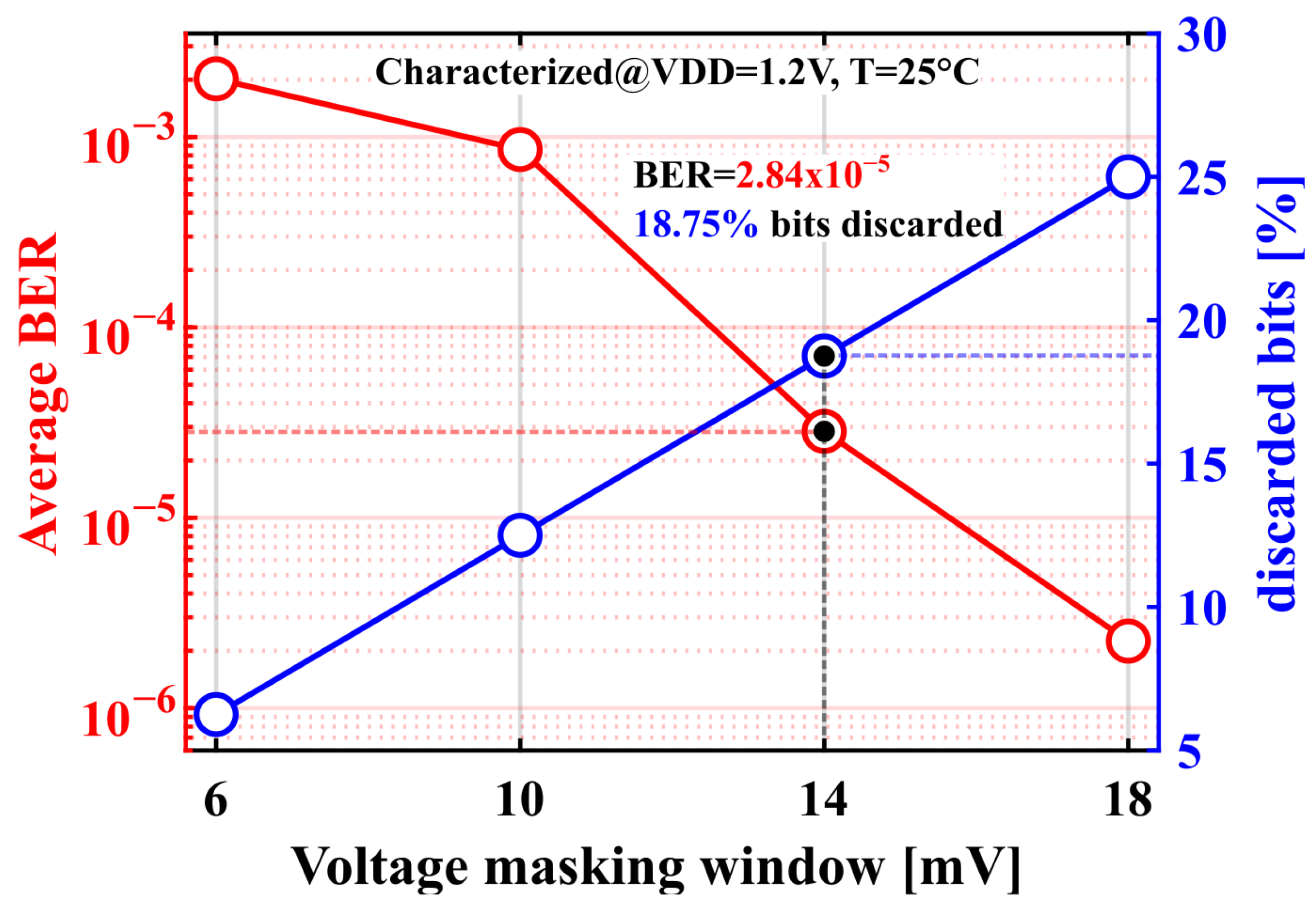
The masking scheme effectively improves the BER, as shown in Figure 3. Under golden key (GK) conditions ( V D D = 1.2 V , T = 25 ° C ), our design shows an average native BER (in 10 samples) of 1.7%. The BER is enhanced by discarding possible noisy bits according to the above-described masking procedure. The average BER is reduced from 0.002 at the | 3 m V | offset mask (voltage masking window = 6 m V ) to 2.25 × 10 6 at 9 m V (voltage masking window = 18 m V ), while the percentage of discarded bits increases from 6.25% to 25%, respectively. At a 14 m V voltage masking window, the obtained BER was 2.84 × 10 5 , with about 19% discarded bits.
Figure 4 shows the impact of V D D (a) and temperature (b) variations on the BER. The shaded regions represent ±3 σ confidence intervals around the mean BER values at each measurement point, capturing the statistical spread across all samples. The initial PUF enrollment was performed under GK conditions, and the BER at each operating point was evaluated against that reference. The mean BER increases from 0.0169@1.2 V to 0.045@0.8 V and 0.027@1.3 V , while maintaining a constant temperature of 25 ° C . At a constant supply voltage of 1.2 V , the native BER reaches its worst case of 0.04 at 0 ° C . While our masking scheme improves the BER by discarding unstable noisy bits, this is not enough to significantly reduce the BER when supply or temperature variations occur. This implies that noise is not the only factor causing bit instability; key-bit flipping can also result from differences in the voltage/temperature dependence of the V th of selected transistors, which may invert the polarity of the V th mismatch [23]. In addition, other sources of instability may become relevant over time due to PUF aging, such as hot carrier injection (HCI) and bias temperature instability (BTI), both of which can cause shifts in V th and consequently lead to bit-flip events in the PUF response. These effects can be mitigated by implementing a periodic re-enrollment procedure, allowing the system to adapt to long-term variations and maintain the reliability of the PUF response.
To counteract the effect of inverted polarity of the V th mismatch, the spatial majority voting (SMV) scheme described in [24] was adopted. In SMV, each bit of the key depends on a group of affiliated bits. For a group of v bits, a fault tolerance of up to (v − 1)/2 bits is guaranteed, where v is an odd integer. SMV was applied to our design in post-processing for a value v = 3. By applying both 14 m V voltage masking and SMV-3, the average BER is improved to 1.58 × 10 4 at 0.8 V and to 8.5 × 10 7 at 1.3 V , as shown in Figure 4a. For 0 ° C and 75 ° C , the average BER is about 4 × 10 4 and 2.5 × 10 4 , respectively (see Figure 4b). Finally, under GK conditions the evaluated BER ranges between 0 and 3.12 × 10 9 (which would correspond to one single-bit error within the number of performed tests). Note that during the measurements under GK conditions, no errors were obtained. Taking into account all examined variations in V D D (from 0.8 V to 1.3 V ) and temperature (from 0 ° C to 75 ° C ), the average native BER is 3.5%. After applying a 14 m V voltage masking and SMV-3 stabilization scheme, the average BER is improved to 9.73 × 10 4 .

3.3. Uniqueness, Uniformity, and Randomness

In this section, our proposed PUF is assessed in relation to figures of merit related to uniqueness, uniformity, and randomness.
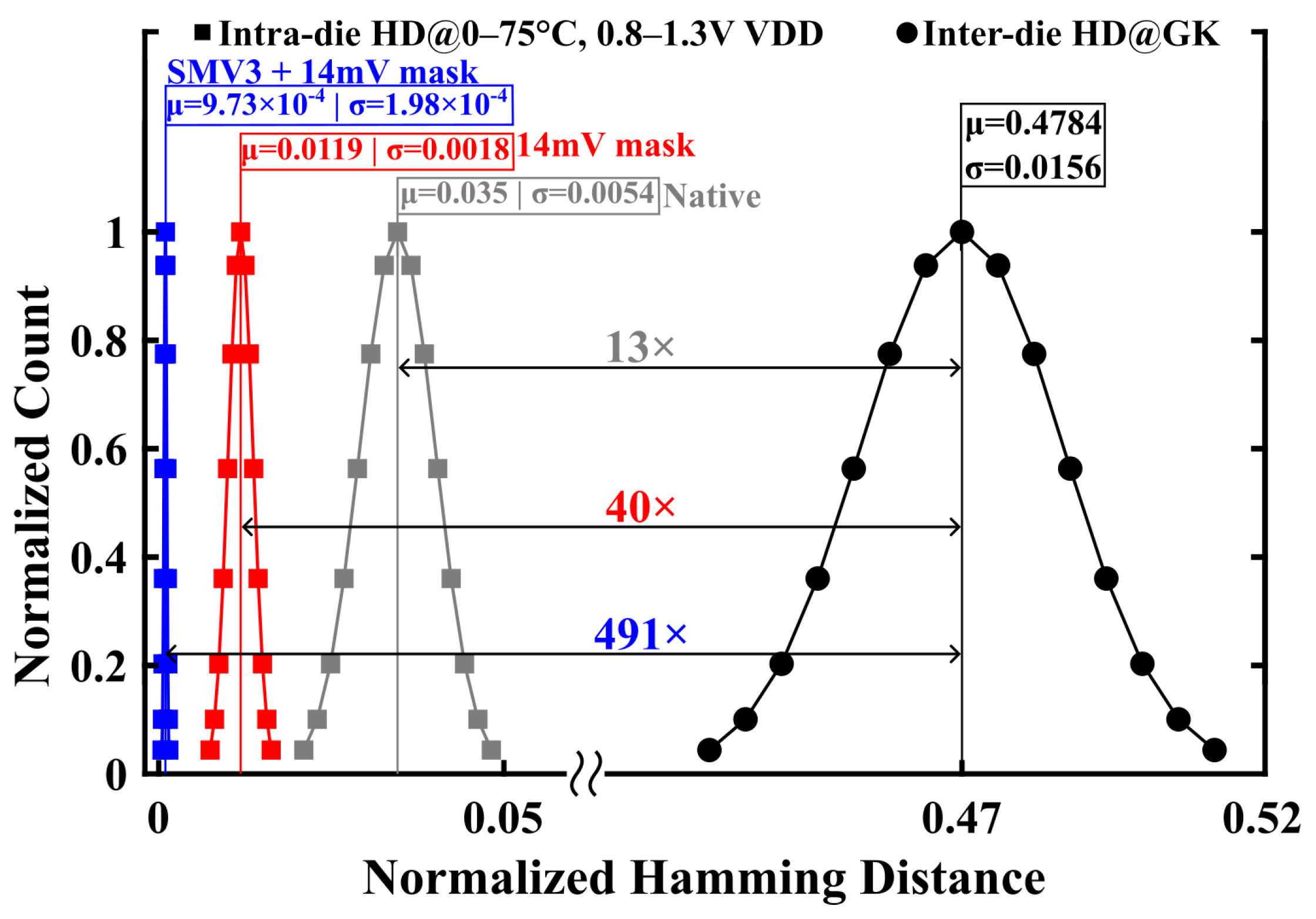
Uniqueness: The normalized (to the length of the PUF response) inter-die Hamming distance (HD) is used to estimate the ability to obtain unique responses for the same address across different PUF chips. From Figure 5, the mean (standard deviation) of the inter-PUF HD is 0.4784 (0.0156), which is quite close to the ideal value of 0.5.
Figure 5 also presents the intra-die HD for the native case, the 14 m V voltage masking case, and the 14 m V masking with SMV-3 case. The intra-die HD was measured across a V D D range of 0.8 V to 1.3 V and a temperature range of 0 ° C to 75 ° C . Identifiability, defined as the inter/intra-HD ratio [2], has been improved from 13× with no stabilization techniques to 491× with the application of voltage masking and SMV.
Uniformity: It estimates the proportion of 1s and 0s in a PUF key, aiming for equal distribution (50%) to ensure random PUF responses. The Hamming Weight (HW) in the GK condition was evaluated to characterize uniformity. In our PUF, the mean measured HW is 0.504, which is very close to the ideal value (0.5), with a standard deviation of 0.009.
Randomness: The NIST SP 800-22 Revision 1a test suite (National Institute of Standards and Technology, Gaithersburg, MD, USA) was used to assess the randomness of the generated bit sequences. Ten chips were evaluated using 150 consecutive challenges, thus producing independent 4800-bit sequences per chip. As shown in Table 1, the average p-values for all tests exceeded the 0.01 threshold, and the NIST pass-rate criterion (≥80% across 10 runs) was satisfied up to a 4800-bit-stream length per chip. Beyond this length, the pass rate gradually decreases, which is reasonable for PUF applications with modest interrogation rates.
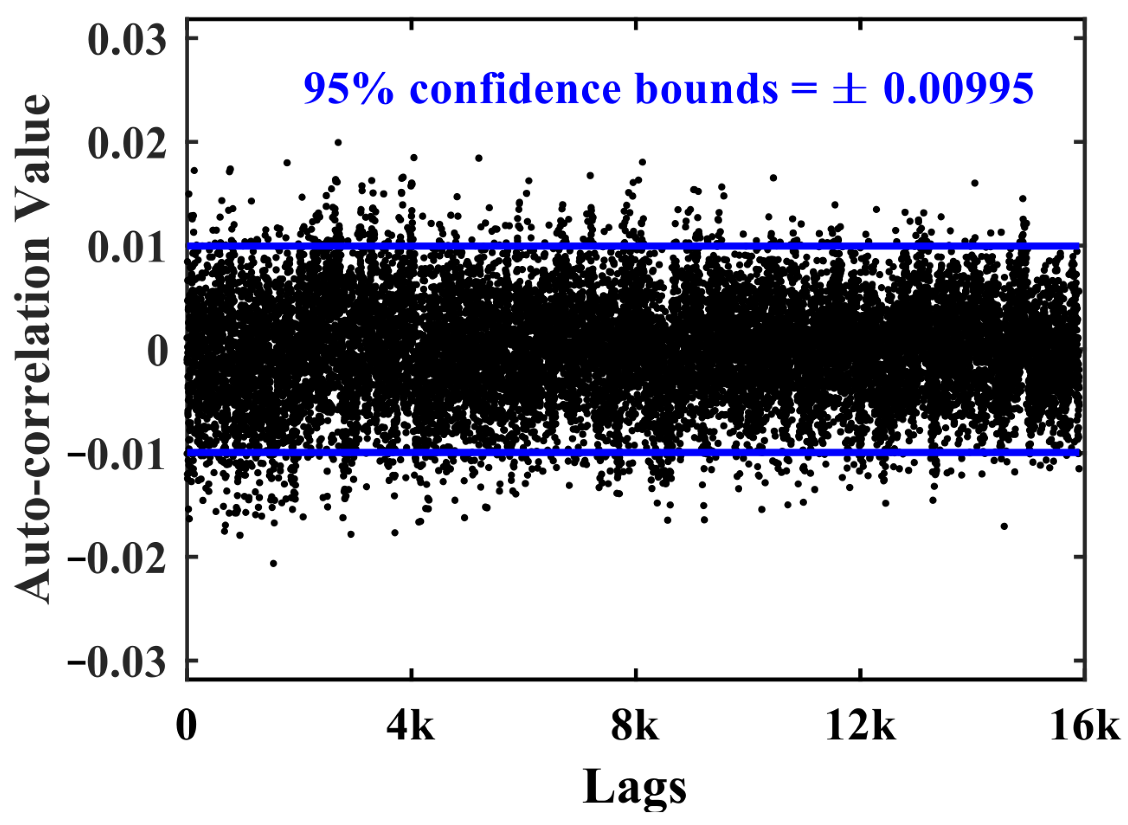
The autocorrelation function (ACF) of our PUF design was also evaluated, as shown in Figure 6. The ACF results demonstrated a 95% confident bound of ±0.00995, closely approximating the ideal value of zero [5].

3.4. Comparison

Table 2 summarizes the performance of our PUF as compared to some state-of-the-art designs. With a competitive native BER across supply voltage and temperature variations of 3.5% and an energy consumption of 1.37 pJ per bit, our design can operate efficiently within a supply voltage range from 0.8 V to 1.3 V , thus outperforming previous works [6,24,25,26], which are limited to narrower voltage operating ranges.
By discarding just 19% of key-bits and applying the SMV-3 stabilization scheme, the BER is lower than 3.12 × 10 9 under GK conditions, or equal to 9.73 × 10 4 when considering supply voltage and temperature variations, which is an overall improvement with respect to the state of the art. Although the design in [25] achieves a zero BER, it does so after hot carrier injection burn-in, which complicates the PUF enrollment phase.
The design presented in [30] was tested with a larger number of evaluations than our PUF solution and shows a V/T-stabilized BER of 4.88 × 10 8 . Although both [25,30] achieved a better BER after stabilization, they also exhibit a higher ACF@95%, implying higher correlation among PUF bits. The ACF exhibited by our PUF (0.00995) ranks second best among competitors, surpassed only by [6,26], which both report an ACF of 0.007.
Further BER improvements in our design can be achieved through more aggressive SMV schemes and/or by masking bits with higher comparator offsets at the cost of an increased masking ratio.
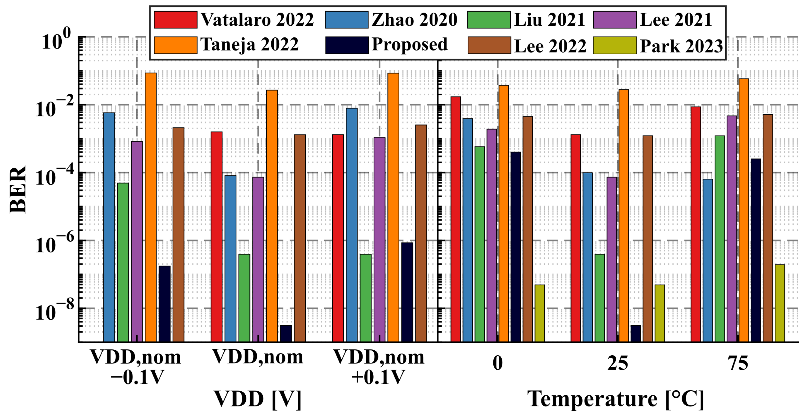
To allow a fairer comparison, Figure 7 shows the BERs for all the evaluated designs across voltage ( V D D , n o m − 0.1 V, V D D , n o m , V D D , n o m + 0.1 V) and temperature (0 ° C , 25 ° C , and 75 ° C ) variations. Our PUF exhibits the lowest BER at V D D , n o m and V D D , n o m − 0.1 V and ranks second at V D D , n o m + 0.1 V. Moreover, across temperature extremes (0 ° C and 75 ° C ), our design maintains competitive BER performance, while achieving the lowest BER value at room temperature (25 ° C ).
In summary, our PUF solution represents a good trade-off between energy efficiency, reliability (low BER), and security (low ACF). This is achieved at the expense of reduced throughput with respect to the designs presented in [24,25,26,30].

4. Conclusions

We proposed a PUF based on a differential PMOS array and a dynamic comparator with a trimmable offset. Our design achieved a zero BER (< 3.12 × 10 9 ) at V D D = 1.2 V and T = 25 ° C after applying a bit masking scheme and spatial majority voting. When taking into account supply voltage (0.8 V –1.3 V ) and temperature (0 ° C –75 ° C ) variations, the measured native BER was 3.5%, enhanced to 9.73 × 10 4 through stabilization techniques, while consuming an energy per bit of about 1.37 pJ.

Author Contributions

Conceptualization, B.Z., S.S., E.G., A.C., G.I. and M.L.; investigation, B.Z., S.S. and M.L.; writing—review and editing, B.Z., S.S., E.G., A.C., G.I. and M.L. All authors have read and agreed to the published version of the manuscript.

Funding

This research was partially supported by the Italian MUR under the Forelab project of the “Dipartimenti di Eccellenza” programme.

Data Availability Statement

The original contributions presented in this study are included in the article. Further inquiries can be directed to the corresponding author(s).

Conflicts of Interest

The authors declare no conflicts of interest.

References

  1. Herder, C.; Yu, M.D.; Koushanfar, F.; Devadas, S. Physical unclonable functions and applications: A tutorial. Proc. IEEE 2014, 102, 1126–1141. [Google Scholar] [CrossRef]
  2. Alvarez, A.B.; Zhao, W.; Alioto, M. Static physically unclonable functions for secure chip identification with 1.9–5.8% native bit instability at 0.6–1 V and 15 fJ/bit in 65 nm. IEEE J. Solid-State Circuits 2016, 51, 763–775. [Google Scholar]
  3. Mexis, N.; Anagnostopoulos, N.A.; Katzenbeisser, S.; Kavun, E.B.; Tehranipoor, S.; Arul, T. Achieving Error-Free Lightweight Authentication With DRAM-Based Physical Unclonable Functions. IEEE Trans. Circuits Syst. I Regul. Pap. 2025, 72, 637–646. [Google Scholar] [CrossRef]
  4. Stanzione, S.; Puntin, D.; Iannaccone, G. CMOS silicon physical unclonable functions based on intrinsic process variability. IEEE J. Solid-State Circuits 2011, 46, 1456–1463. [Google Scholar] [CrossRef]
  5. Vatalaro, M.; Rose, R.D.; Maccaronio, V.; Lanuzza, M.; Crupi, F. Highly Stable PUFs Based on Stacked Voltage Divider for Near-Zero BER Native Sensitivity to Voltage Variations. IEEE Trans. Circuits Syst. I Regul. Pap. 2024, 72, 521–534. [Google Scholar] [CrossRef]
  6. Lee, J.; Kim, M.; Jeong, M.; Shin, G.; Lee, Y. A 20F2/Bit Current-Integration-Based Differential nand-Structured PUF for Stable and V/T Variation-Tolerant Low-Cost IoT Security. IEEE J. Solid-State Circuits 2022, 57, 2957–2968. [Google Scholar] [CrossRef]
  7. Alioto, M. Trends in Hardware Security: From Basics to ASICs. IEEE Solid-State Circuits Mag. 2019, 11, 56–74. [Google Scholar] [CrossRef]
  8. Amirany, A.; Mohebbi, L. SQTRNG: Spintronic Quaternary True Random Number Generator. SPIN 2025, 15. [Google Scholar] [CrossRef]
  9. Lim, S.; Song, B.; Jung, S.O. Highly independent MTJ-based PUF system using diode-connected transistor and two-step postprocessing for improved response stability. IEEE Trans. Inf. Forensics Secur. 2020, 15, 2798–2807. [Google Scholar] [CrossRef]
  10. Lee, S.; Kang, J.; Kim, J.M.; Kim, N.; Han, D.; Lee, T.; Ko, S.; Yang, J.; Lee, S.; Lee, S.; et al. Spintronic physical unclonable functions based on field-free spin–orbit-torque switching. Adv. Mater. 2022, 34, 2203558. [Google Scholar] [CrossRef] [PubMed]
  11. Maes, R. Physically Unclonable Functions: Constructions, Properties and Applications; Springer: Berlin/Heidelberg, Germany, 2013. [Google Scholar]
  12. Tran, S.; Ngo, C.T.; Pham, V.K.; Hong, J.P. A Lightweight ECC-Compatible End-to-End Security Protocol Using CRP-PUF and TRNG for IoT Devices. IEEE Internet Things J. 2025; early access. [Google Scholar]
  13. Qureshi, M.A.; Munir, A. PUF-RAKE: A PUF-based robust and lightweight authentication and key establishment protocol. IEEE Trans. Dependable Secur. Comput. 2021, 19, 2457–2475. [Google Scholar] [CrossRef]
  14. Liu, J.; Zhao, Y.; Zhu, Y.; Chan, C.H.; Martins, R.P. A Weak PUF-Assisted Strong PUF With Inherent Immunity to Modeling Attacks and Ultra-Low BER. IEEE Trans. Circuits Syst. I Regul. Pap. 2022, 69, 4898–4907. [Google Scholar] [CrossRef]
  15. Mathew, S.K.; Satpathy, S.K.; Anders, M.A.; Kaul, H.; Hsu, S.K.; Agarwal, A.; Chen, G.K.; Parker, R.J.; Krishnamurthy, R.K.; De, V. 16.2 A 0.19pJ/b PVT-variation-tolerant hybrid physically unclonable function circuit for 100% stable secure key generation in 22nm CMOS. In Proceedings of the 2014 IEEE International Solid-State Circuits Conference Digest of Technical Papers (ISSCC), San Francisco, CA, USA, 9–13 February 2014; pp. 278–279. [Google Scholar] [CrossRef]
  16. Shifman, Y.; Shor, J. Preselection Methods to Achieve Very Low BER in SRAM-Based PUFs—A Tutorial. IEEE Trans. Circuits Syst. II Express Briefs 2022, 69, 2551–2556. [Google Scholar] [CrossRef]
  17. He, Z.; Chen, W.; Zhang, L.; Chi, G.; Gao, Q.; Harn, L. A Highly Reliable Arbiter PUF With Improved Uniqueness in FPGA Implementation Using Bit-Self-Test. IEEE Access 2020, 8, 181751–181762. [Google Scholar] [CrossRef]
  18. He, Y.; Li, D.; Yu, Z.; Yang, K. An automatic self-checking and healing physically unclonable function (PUF) with <3 × 10−8 bit error rate. In Proceedings of the 2021 IEEE International Solid-State Circuits Conference (ISSCC), Online, 13–22 February 2021; IEEE: San Francisco, CA, USA, 2021; Volume 64, pp. 506–508. [Google Scholar]
  19. Al-Tamimi, A.; Ali, S.; Cao, Y.; Bermak, A. Threshold voltage based dual memristor crossbar PUF. AEU-Int. J. Electron. Commun. 2024, 175, 155012. [Google Scholar] [CrossRef]
  20. Ni, L.; Zhang, J. S2RAM PUF: An ultra-low power subthreshold SRAM PUF with zero bit error rate. In Proceedings of the 61st ACM/IEEE Design Automation Conference, San Francisco, CA, USA, 23–27 June 2024; pp. 1–6. [Google Scholar]
  21. Zambrano, B.; Garzón, E.; Strangio, S.; Iannaccone, G.; Lanuzza, M. A 0.6 V–1.8 V Compact Temperature Sensor With 0.24 °C Resolution, ±1.4 °C Inaccuracy and 1.06 nJ per Conversion. IEEE Sens. J. 2022, 22, 11480–11488. [Google Scholar] [CrossRef]
  22. Tang, X.; Shen, L.; Kasap, B.; Yang, X.; Shi, W.; Mukherjee, A.; Pan, D.Z.; Sun, N. An Energy-Efficient Comparator With Dynamic Floating Inverter Amplifier. IEEE J. Solid-State Circuits 2020, 55, 1011–1022. [Google Scholar] [CrossRef]
  23. Böhm, C.; Hofer, M. Physical Unclonable Functions in Theory and Practice; Springer Science & Business Media: New York, NY, USA, 2012. [Google Scholar]
  24. Zhao, Q.; Wu, Y.; Zhao, X.; Cao, Y.; Chang, C.H. A 1036-F2/Bit High Reliability Temperature Compensated Cross-Coupled Comparator-Based PUF. IEEE Trans. Very Large Scale Integr. (VLSI) Syst. 2020, 28, 1449–1460. [Google Scholar] [CrossRef]
  25. Liu, K.; Chen, X.; Pu, H.; Shinohara, H. A 0.5-V Hybrid SRAM Physically Unclonable Function Using Hot Carrier Injection Burn-In for Stability Reinforcement. IEEE J. Solid-State Circuits 2021, 56, 2193–2204. [Google Scholar] [CrossRef]
  26. Taneja, S.; Rajanna, V.K.; Alioto, M. In-Memory Unified TRNG and Multi-Bit PUF for Ubiquitous Hardware Security. IEEE J. Solid-State Circuits 2022, 57, 153–166. [Google Scholar] [CrossRef]
  27. Vatalaro, M.; De Rose, R.; Lanuzza, M.; Crupi, F. Static CMOS physically unclonable function based on 4T voltage divider with 0.6%–1.5% bit instability at 0.4–1.8 V operation in 180 nm. IEEE J. Solid-State Circuits 2022, 57, 2509–2520. [Google Scholar] [CrossRef]
  28. Liang, Z.Y.; Wei, H.H.; Liu, T.T. A Wide-Range Variation-Resilient Physically Unclonable Function in 28 nm. IEEE J. Solid-State Circuits 2020, 55, 817–825. [Google Scholar] [CrossRef]
  29. Lee, J.; Lee, D.; Lee, Y.; Lee, Y. A 354F2 Leakage-Based Physically Unclonable Function With Lossless Stabilization Through Remapping for Low-Cost IoT Security. IEEE J. Solid-State Circuits 2021, 56, 648–657. [Google Scholar] [CrossRef]
  30. Park, J.; Sim, J.Y. A Reconfigurable LDO-Assisted Physically Unclonable Function Achieving a Zero-BER With 14% Masking. IEEE Trans. Circuits Syst. I Regul. Pap. 2023, 70, 3244–3253. [Google Scholar] [CrossRef]
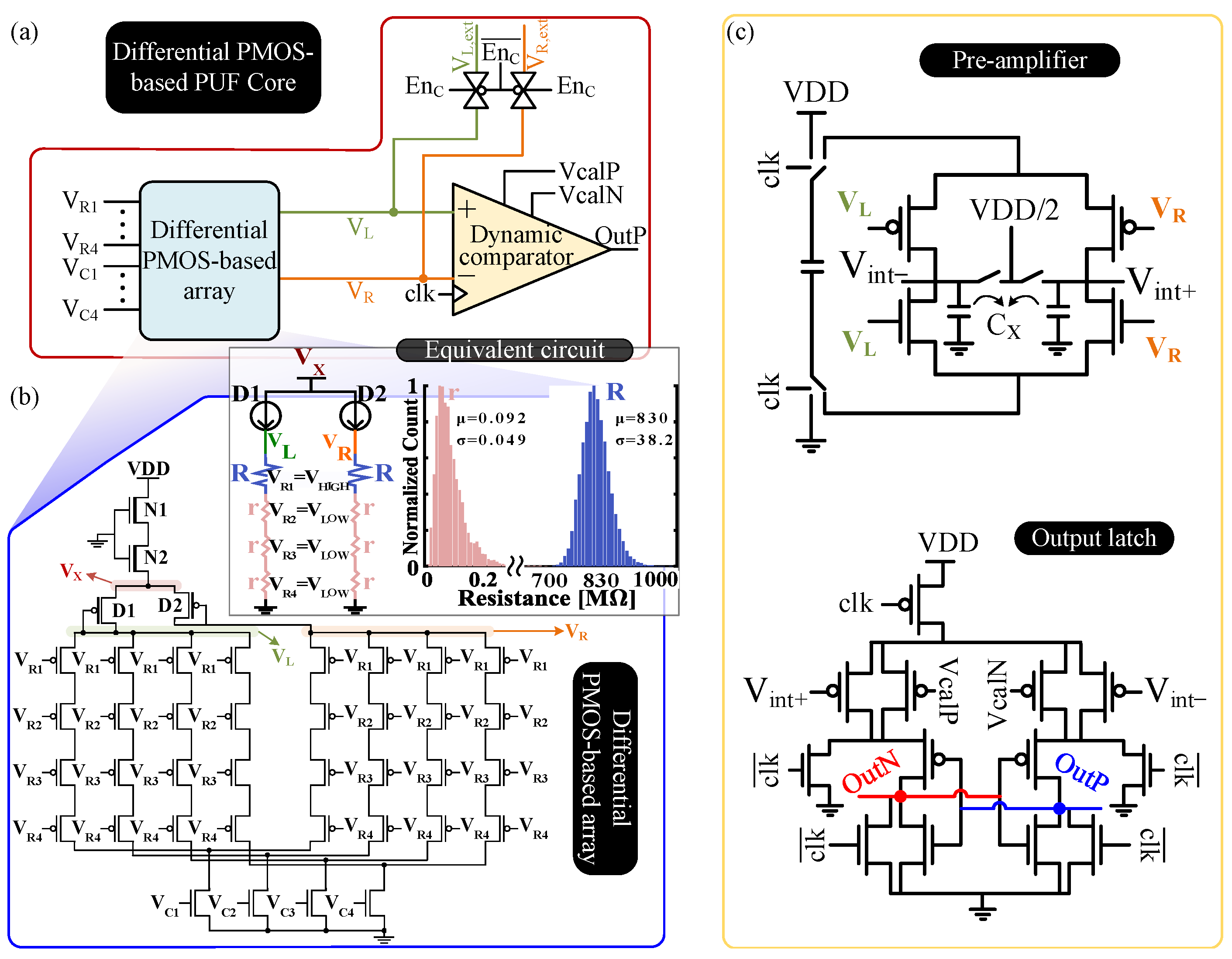
Figure 1. (a) Differential PMOS-based PUF core. (b) Differential PMOS array. (c) Dynamic comparator.
Jlpea 15 00053 g001
Figure 2. (a) Test chip design. (b) Layouts of 8 × 4 PUF array and 32-bit shift register. (c) Chip micrograph. (d) Measurements setup.
Jlpea 15 00053 g002
Figure 3. Average BER and average percentage of discarded bits versus voltage masking window (2 · δ   m V ).
Jlpea 15 00053 g003
Figure 4. BER across (a) supply voltage and (b) temperature variations. The bands represent a 3-sigma deviation from the mean.
Jlpea 15 00053 g004
Figure 5. Normalized intra-die and inter-die Hamming distances.
Jlpea 15 00053 g005
Figure 6. Autocorrelation function (ACF) of our PUF implementation.
Jlpea 15 00053 g006
Figure 7. BER comparison of proposed PUF with the state of the art (Vatalaro 2022 [27], Zhao 2020 [24], Liu 2021 [25], Lee 2021 [29], Taneja 2022 [26], Lee 2022 [6] and Park 2023 [30]) across supply voltage and temperature variations.
Jlpea 15 00053 g007
Table 1. NIST SP800-22 test suite results.
Test NameStream LengthNumber of RunsAverage p-ValuePass (%)
ine Frequency4800100.32790
Block Frequency4800100.08990
Cumulative Sums
(Forward)
4800100.07680
Cumulative Sums
(Reverse)
4800100.05280
Runs4800100.09880
Longest Run
of Ones
4800100.1790
FFT4800100.215100
Approximate
Entropy
4800100.10380
Serial4800100.17780
Table 2. Comparison with the state of the art.
This WorkJSSC’22 [27]JSSC’21 [25]TVLSI’20 [24]JSSC’20 [28]JSSC’21 [29]JSSC’22 [26]TCAS-I’23 [30]JSSC’22 [6]
Tech. [nm]6518013065281802840180
Area [ μ m 2 ]45,286300,11539,9352750 8000 ( a ) -15,400--
Area/bit [ μ m 2 ]18.931028.44.382611.480.8819.770.66
Area/bit [F2]44803148497103633,163354112512,35620
Array size512b8 × 3216 × 6416 × 16128b64 × 16-128b256 × 32
Uniqueness0.47840.4930.48730.49530.49940.49460.5030.5027--
Uniformity0.504--0.4980.506-0.503---
Stabilization
method
Offset mask +
SMV3
-HCI Burn-inTMV +
DBD +
SMV
Delay calibration
+ TMV7
TMV11 +
Remapping
-DBDTrimming +
TMV11
Remapping +
TMV11
Native
BER@GK
1.69%0.16%0.29%0.44%1.40%0.43%1.80%1.33%0.937%
Native
BER across
V/T variations
3.5%0.65% (b)
 0.5% (c)
1.37% (0.7 V)
 5.76% (120 C)
3.13%8.4% (0.4 V)
 4.5% (125 C)
3.51% (1.8 V)
 4.2% (80 C)
6.70%0.297%2.26% (1.9 V)
4.54% (−20 C)
Stabilized
BER across
V/T variations
9.73 × 10 4 -0%0.69%0.55% (b)
 0.078% (c)
0.43% (1.8 V)
 0.47% (80 C)
- 4.88 × 10 8 0.331% (1.9 V)
0.633% (−20 C)
0.726% (1.9 V)
 1.362% (−20 C)
Masking ratio19%--4%---14%20%0%
ACF@95%0.009950.04720.03340.01970.0410.01390.0070.04240.007
VDD Range [V]0.8–1.30.4–1.80.5–0.71–1.40.4–1.31–1.80.75–1.050.9–1.41.5–1.9
Temperature
range [ ° C]
0–7510–80−40–120−50–150−40–1250–80−25–100−40–125−20–80
Energy/bit [J]1.37p-2.07f@0.5V2.98p2.15p465p72f0.186p138p
Throughput [b/s]8 K-23 M8 M-0.65 K12.6 M69.9 M1.6 K
(a) Only array area is reported. (b) Obtained over a supply voltage sweep. (c) Obtained over a temperature sweep.
Disclaimer/Publisher’s Note: The statements, opinions and data contained in all publications are solely those of the individual author(s) and contributor(s) and not of MDPI and/or the editor(s). MDPI and/or the editor(s) disclaim responsibility for any injury to people or property resulting from any ideas, methods, instructions or products referred to in the content.