Article

Analytical Implementation of Electron–Phonon Scattering in a Schottky Barrier CNTFET Model

by
Ibrahim L. Abdalla
1,
Fatma A. Matter
2,
Ahmed A. Afifi
2,
Mohamed I. Ibrahem
3,*,
Hesham F. A. Hamed
4,5 and
Eslam S. El-Mokadem
2
1
Department of Electronics and Communications Engineering, Zagazig University, Zagazig 44519, Egypt
2
Department of Electronics and Communication Engineering, Higher Technological Institute, 10th of Ramadan City 44629, Egypt
3
School of Computer and Cyber Sciences, Augusta University, Augusta, GA 30912, USA
4
Electrical Engineering Department, Faculty of Engineering, Minia University, Minya 61519, Egypt
5
Telecommunication Engineering Department, Egyptian Russian University, Badr City 11829, Egypt
*
Author to whom correspondence should be addressed.
J. Low Power Electron. Appl. 2025, 15(2), 28; https://doi.org/10.3390/jlpea15020028
Submission received: 1 March 2025 / Revised: 10 April 2025 / Accepted: 30 April 2025 / Published: 2 May 2025

Abstract

:
This paper elaborates on the proposal of a new analytical model for a non-ballistic transport scenario for Schottky barrier carbon nanotube field effect transistors (SB-CNTFETs). The non-ballistic transport scenario depends on incorporating the effects of acoustic phonon (A-Ph) and optical phonon (O-Ph) electron scattering mechanisms. The analytical model is rooted in the solution of the Landauer integral equation, which is modified to account for non-ballistic transport through a set of approximations applied to the Wentzel–Kramers–Brillouin (WKB) transmission probability and the Fermi–Dirac distribution function. Our proposed model was simulated to evaluate the total current and transconductance, considering scenarios both with and without the electron–phonon scattering effect. The simulation results revealed a substantial decrease of approximately 78.6% in both total current and transconductance due to electron–phonon scattering. In addition, we investigated the impact of acoustic phonon (A-Ph) and optical phonon (O-Ph) scattering on the drain current under various conditions, including different temperatures, gate lengths, and nanotube chiralities. This comprehensive analysis helps in understanding how these parameters influence device performance. Compared with experimental data, the model’s simulation results demonstrate a high degree of agreement. Furthermore, our fully analytical model achieves a significantly faster runtime, clocking in at around 2.726 s. This validation underscores the model’s accuracy and reliability in predicting the behavior of SB-CNTFETs under non-ballistic conditions.

1. Introduction

The International Roadmap for Devices and Systems (IRDS) has identified key requirements for advancing CMOS technology, including high-mobility channel materials, supply voltages below 0.6 V, gate-all-around (GAA) structures, and the fabrication of advanced nonplanar multi-gate and nanowire MOSFETs [1,2,3,4,5,6]. In this context, carbon nanotube FETs (CNTFETs) have emerged as promising candidates to meet these IRDS targets [7,8,9,10,11], owing to their unique quasi-one-dimensional (1D) structure, high carrier velocity, excellent thermal conductivity, and near-ballistic transport characteristics.
In high-quality intrinsic carbon nanotubes, electron–phonon scattering emerges as the dominant scattering mechanism. This phenomenon occurs when electron transport is perturbed by quantized lattice vibrations (phonons). Notably, electron–electron scattering effects are typically negligible in these systems due to the reduced density of states in one-dimensional structures and efficient screening effects [9,12,13,14,15,16].
The unique properties of intrinsic carbon nanotubes (CNTs) establish electron–phonon interactions as the dominant scattering mechanism. This predominance stems from several key characteristics: First, CNTs possess an exceptionally ordered crystalline structure with minimal defects or impurities, significantly reducing potential scattering centers. Second, their quasi-one-dimensional nature inherently limits electron scattering pathways compared to bulk materials. Third, CNTs exhibit remarkably high carrier mobilities, allowing nearly unimpeded electron transport [17]. When scattering does occur, it arises primarily from phonon interactions—particularly at elevated temperatures where lattice vibrations intensify. Collectively, these attributes render electron–phonon scattering the critical factor governing CNT performance.
Electron–phonon scattering in carbon nanotubes occurs through two primary mechanisms: acoustic phonon (A-Ph) and optical phonon (O-Ph) interactions. In Schottky barrier carbon nanotube field-effect transistors (SB-CNTFETs), acoustic phonon scattering dominates low-temperature transport [18,19]. This process involves momentum exchange between electrons and the crystal lattice, leading to energy dissipation. The acoustic phonon (A-Ph) modes—including both longitudinal and transverse types—play a crucial role in determining carrier mobility and consequently current flow through the nanotube channel. Their dispersion relation, characterized by frequency dependence on wave vector (k), is essential for understanding electron–phonon interactions.
In contrast, optical phonon (O-Ph) scattering becomes significant at elevated temperatures. Unlike acoustic phonons, optical modes exhibit fixed frequencies for given vibration patterns, enabling substantial electron energy transitions that markedly affect current characteristics. Both longitudinal optical (LO) and transverse optical (TO) phonons contribute to increased scattering rates, which reduce effective mobility and promote non-ballistic transport behavior [20,21].
The analysis of phonon scattering mechanisms has been extensively performed by various techniques, including non-equilibrium green function (NEGF) and Monte Carlo semi-classical simulation [22,23,24,25]. Although these computational techniques yield realistic simulation results, they are impractical in terms of memory usage and computing time. One of the primary challenges in developing a circuit-level model is the execution time. Initially, this concern led us to seek an analytical solution for the Landauer integral current equation. In our current research, we have developed and validated a physical analytical model by making a set of approximations of probability functions in the current equation. This model effectively considers the primary scattering effects in Schottky barrier carbon nanotube field-effect transistors (SB-CNTFETs), specifically electron–phonon scattering, under non-ballistic transport conditions.
The proposed model introduces several novel features:
  • It adopts a fully analytical approach, which significantly enhances runtime performance.
  • The model encompasses critical factors such as non-ballistic transport and transmission through Schottky barrier (SB) contacts.
  • It employs specific and detailed formulations for both acoustic phonon (A-Ph) and optical phonon (O-Ph) electron scattering processes.
This paper is organized as follows: After the introduction, Section 2 presents the physical and mathematical transport model that accounts for acoustic phonon (A-Ph) and optical phonon (O-Ph) scattering. Section 3 carries out complete simulations of I d s versus V g s and I d s versus V d s comparing these results with their ballistic counterparts (without scattering). Section 4 concludes the work.

2. Transport Model

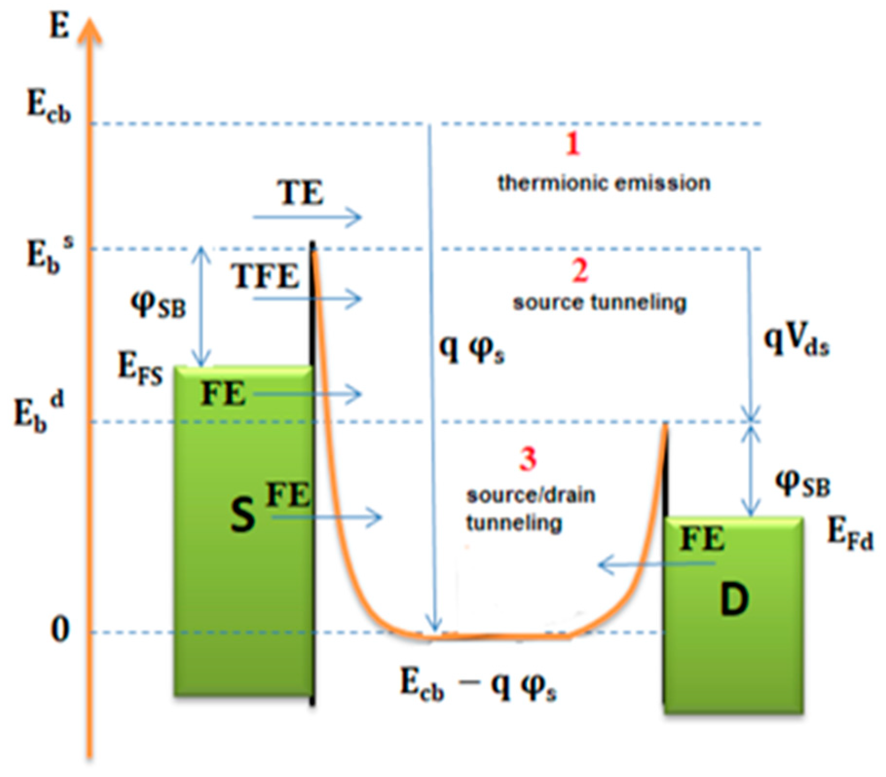
2.1. SB-CNTFET Physical Model

The conduction band profile of the SB-CNTFET is displayed in Figure 1, which illustrates the various mechanisms by which the device injects electrons. Under the presence of a Schottky barrier (SB) at the source and drain, the energy band can be categorized into three distinct regions. The first region, characterized by thermionic current, occurs when electrons possess enough energy to surmount the source potential barrier, allowing them to flow from the source into the channel without reflection. In the second region, electrons with energies below the source potential barrier tunnel through the channel toward the drain, as their energy suffices to cross the drain potential barrier without reflection. Conversely, electrons moving from the drain to the source in the opposite direction exhibit the same behavior. In the third region, due to their low energy, electrons tunnel from both the source and drain. The electrons in each of the three regions are characterized by three distinct types of currents, as categorized earlier. For region 1, the current is represented by thermionic emission (TE). In region 2, the electron flow is represented by the field emission (FE) and the thermionic field emission (TFE) currents. Lastly, region 3 is characterized by field emission tunneling, wherein electrons tunnel from both the source and the drain. This tunneling represents the dominant mechanism of electron flow in this region.
The model’s energy reference point is situated at the bottom of the first conduction sub-band, given by E c b q   φ S , as shown in Figure 1. Here, φ S denotes the surface potential and E g signifies the energy band gap ( E c b = E g / 2 ). The channel’s total length,   L , is commonly referred to as the gate length, L G . With respect to the energy reference point, the Fermi levels at the source and drain are represented by ( E F S ( d ) ) as illustrated in Equation (1). The potential barrier heights at both the source and drain, relative to the reference point, are denoted by ( E b S ( d ) ) as depicted in Equation (2).
E F S ( d ) = q φ S E c b q V s ( d )
E b S ( d ) = φ S B + q φ S E c b q V s ( d )
where φ S B is the Schottky barrier height with respect to E F s d .

2.2. Electron–Phonon Scattering

Carrier transport in CNTs is significantly impacted by electron–phonon scattering [13]. At high biases or finite temperatures, this process becomes especially significant. Electron–phonon scattering can be divided into two categories: high energy (optical phonon scattering) and low energy (acoustic phonon scattering), as described in [26,27]. Each type of scattering mechanism is characterized by its own mean free path. L A P h denotes the electron mean-free path due to acoustic phonon scattering, and L O P h represents the mean free path associated with optical phonon scattering. For electrons undergoing scattering by both acoustic and optical phonons, L e f f is defined using the Mathiessen law, as shown in Equation (3) [28], and its value depends on temperature, bias potential, and the diameter of the nanotube.
L e f f 1 = L A P h 1 + L O P h 1
L e f f = f T , ε , d t
where T represents the temperature, ε denotes the applied field or bias, which can be expressed as ε = V L (with V representing voltage and L standing for the length of the carbon nanotube, or CNT), and d t signifies the CNT diameter.

2.2.1. Acoustic Phonon Scattering (A-Ph)

Electrons with low energy, after being scattered by acoustic phonons, traverse the channel with a certain probability [26].
T A P h = L A P h L A P h + L G
where L A P h depends on CNT chirality (CNT diameter) and temperature as shown in Equations (6) and (7) [28].
L A P h = α A P h   d t T
where α A P h = 400 ~ 565 × 10 3   K
L A P h T = L A P h , 300 × T 300 T
where L A P h , 300 represents the acoustic phonon means free path at room temperature, specifically at T 300 = 300   K .

2.2.2. Optical Phonon Scattering (O-Ph)

High-energy electrons may undergo backscattering due to the emission of optical phonons, which typically have an energy of about ħ ω O P h 0.16   eV . Under high bias conditions, scattering due to optical phonons (O-Ph) emerges as the dominant mechanism [29]. Carriers with energies surpassing ħ ω O P h are prone to backscattering, which significantly diminishes their effective mean free path. For the sake of simplifying the compact model, it is assumed that carriers with energy exceeding ħ ω O P h are backscattered at a consistent rate, determined by a constant transmission probability as illustrated in Equation (8) [26].
T O P h = L O P h L O P h + L G

2.3. SB-CNTFET Current Equation

The electron current in an SB-CNTFET is determined using the Landauer–Büttiker formalism, as described by the integral in Equation (9) [30].
I e = 4 q h 0 T t u n n E f F D E E F S f F D E E F d d E
where f F D E E F represents the Fermi–Dirac distribution function. It illustrates the probability that electrons in the source and drain contacts are occupied [16].
f F D E E F S ( d ) = 1 e x p E E F S ( d ) K B   T + 1
where K B   is Boltzmann’s constant and T is temperature.
T t u n n E represents the total transmission probability, which accounts for electron–phonon scattering.
T t u n n E = T S B S E   T S B d ( E )   T E l P h   S c a t t E
As shown in Equation (11), T t u n n E comprises two probabilities; the first is SB transmission T S B S ( d ) E , which describes electron tunneling through SB at source and drain, respectively. This is crucial for determining the current conducted by the device via tunneling. The barrier height at the interfaces of the device structure significantly influences this probability. Specifically, the electron energy, the effective mass of the charge carriers, and the potential barrier height at the interfaces all affect the transmission probability. To calculate this, we employ the Wentzel–Kramers–Brillouin (WKB) approximation method, as outlined in Equations (12) and (13) [29,31].
T S B S d E = 1                                                                                                                 E b S d < E       exp α E b S d   γ E E b S d       0 < E < E b S d    
γ S B x = 1 x x   t a n 1 1 x x , x = E E b S ( d )
Here, α = 4 λ m ħ , where electron effective mass m is given by m = 8   E c b ħ 2   3   a 2 V π 2 and the π-π bond energy in the tight-binding model is approximately Vπ ≈ 3.033 eV. The carbon–carbon atom distance, denoted by a = 2.49   A ° , represents the underlying CNT Bravais lattice constant. It is equal to 3   a c c , where a c c is the carbon–carbon bond length, approximately 1.42 A ° ( a c c = 1.42   A ° ) [28]. The second probability is   T E l P h   S c a t t E , describes electron–phonon scattering within the channel.
  T E l P h   S c a t t E = L e f f L e f f + L G
where L e f f will be as in Equation (3).
At a low energy ( E < ħ ω O P h ) , (A-Ph) scattering is dominant, and (O-Ph) cannot occur. In this case, L e f f is simplified to L e f f = L A P h .
  T E l P h   S c a t t ( L o w ) = T A P h
At a higher energy ( E ħ ω O P h ) , both scattering mechanisms become effective, and the scattering probability   T E l P h   S c a t t ( H i g h ) will be as described in Equation (14).
  T E l P h   S c a t t ( H i g h ) =   T E l P h   S c a t t E

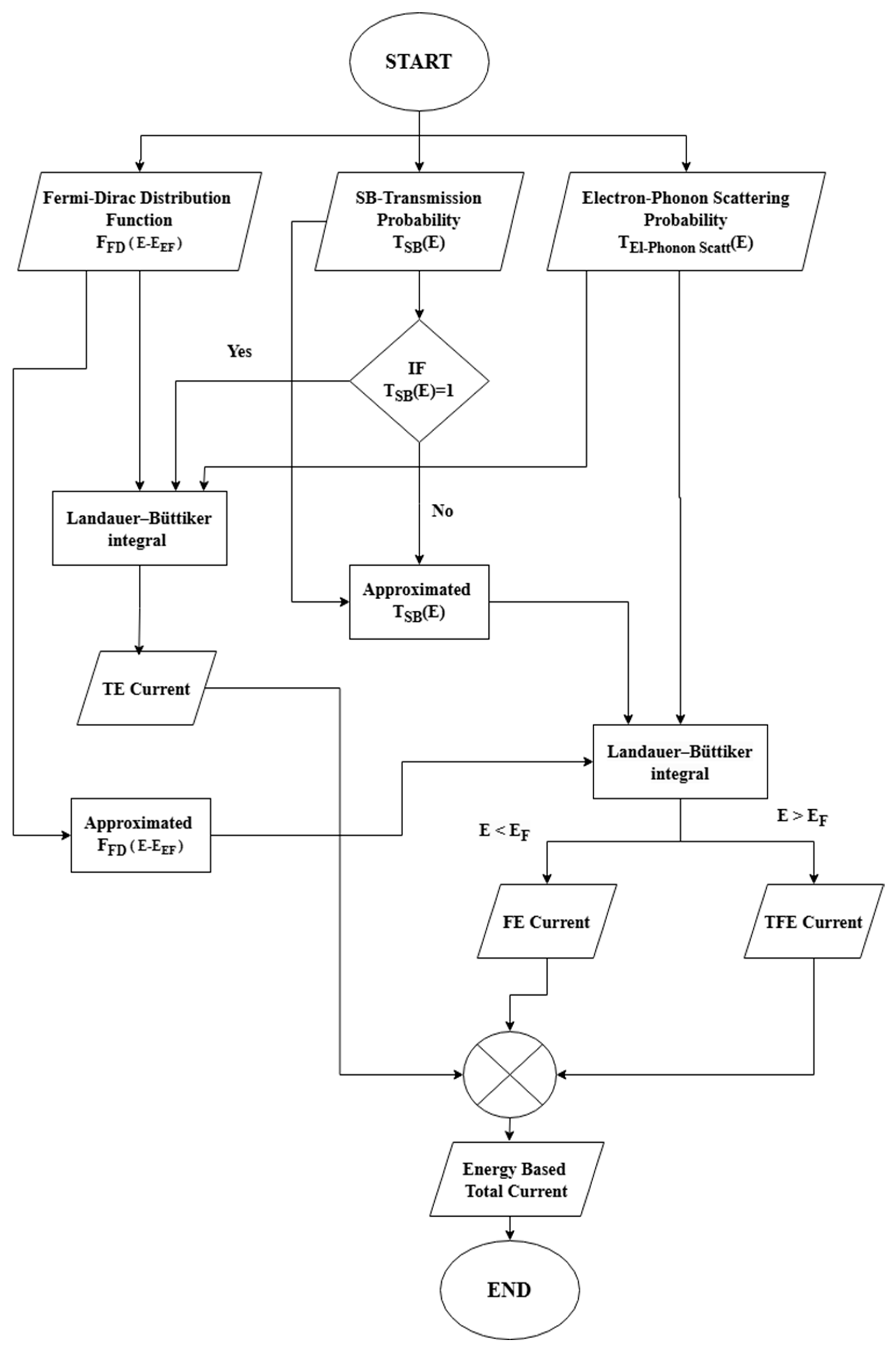
2.4. Mathematical Model

In this section, the analytical model approach for the total current is presented.

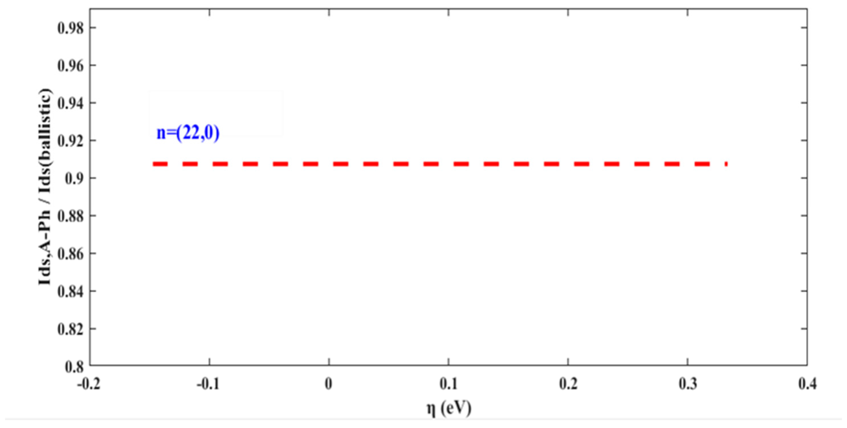
2.4.1. Effect of Acoustic Phonon Only (A-Ph)

When only acoustic phonons scatter electrons, the source and drain current components are illustrated by Equation (17).
I S ( d ) A P h = 4 q   T A P h h × 0 T S B S E   T S B d ( E ) f F D E E F S ( d ) d E

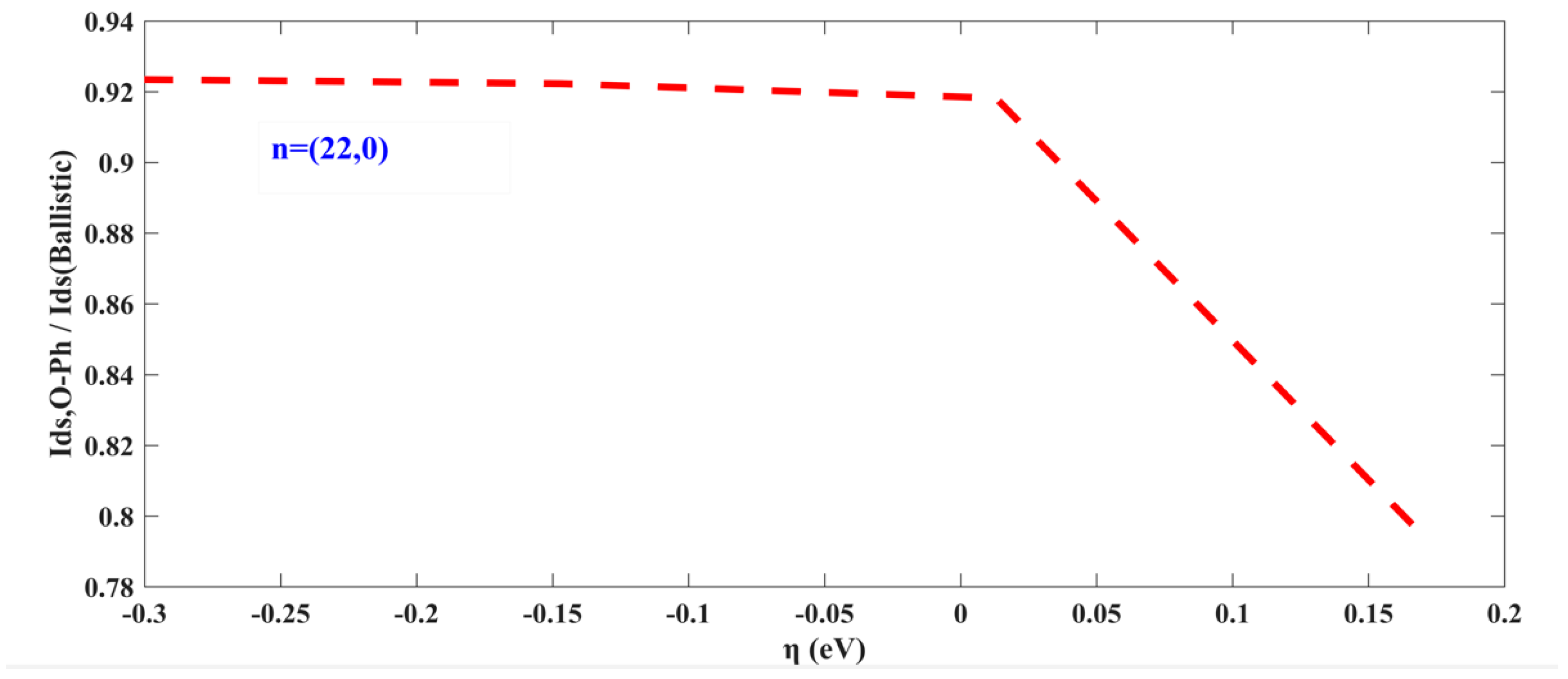
2.4.2. Effect of Optical Phonon Only (O-Ph)

When only optical phonons scatter electrons, the source and drain current components are illustrated by Equation (18).
I S ( d ) O P h = 4 q h ×   0 ħ ω O P h T S B S E   T S B d ( E ) f F D E E F S ( d ) d E + ħ ω O P h   T O P h   T S B S E   T S B d ( E ) f F D E E F S ( d ) d E

2.4.3. Effect of Both Acoustic and Optical Phonons

At low energies E < ħ ω O P h , acoustic phonon scattering dominates, the source and drain current components are determined by Equation (19) similar to Equation (17).
I S ( d ) = 4 q   T E l P h   S c a t t ( L o w ) h × 0 T S B S E   T S B d ( E ) f F D E E F S ( d ) d E
In addition, at high energies ( E ħ ω O P h ) , both acoustic and optical phonons scatter electrons. The source current and drain current components are illustrated by Equations (20) and (21), respectively.
I S = 4 q h [   T E l P h   S c a t t ( L o w ) × 0 T S B S E   T S B d ( E ) f F D E E F S d E   T E l P h   S c a t t ( L o w )   T E l P h   S c a t t ( H i g h ) × 0 T S B S E   T S B d ( E ) f F D E E F S d E ]
I d = 4 q   T E l P h   S c a t t ( H i g h ) h × 0 T S B S E   T S B d ( E ) f F D E E F d d E
I T = I S I d
Forward inelastic scattering (e.g., low-energy phonon absorption) is omitted in Equations (19) and (20) because its net effect on current is secondary to backscattering-dominated processes. The dominant optical phonon backscattering and acoustic phonon scattering are the primary drivers of mobility reduction.
Our analytical model approach relies on the following steps. First, obtaining a good approximation of both the Fermi–Dirac distribution function, f F D ( a p p ) E E F S ( d ) , and the SB transmission probability, T S B ( a p p ) s d E , as illustrated by Equations (23) and (24), respectively, in the current equation.
f F D ( a p p ) E E F           = 1 0.5 exp b 1 E E F K B T                                 E < E F 0.5   e x p b 1 E E F K B T     E F E E F + b 2 K B T exp E F E K B T                         o t h e r w i s e                      
T S B ( a p p ) S ( d ) = e x p α E b S d   γ S B ( a p p ) E E b S d
where γ S B a p p x = P x P + 1 x + 1 and P ≈ 0.7113.
For region 1, where E > E b S , thermally excited electrons propagate into channel without any tunneling so T S B S ( d ) = 1 (TE current from both the source and drain contact).
For region 2, in the range E b d < E < E b S , electrons tunnel through the SB located at the source only. Here, T S B S = T S B a p p S ,   T S B d = 1 (TFE and FE currents from the source contact and TE current from the drain contact).
T S B a p p S = e x p A 1 E + B 1 E C 1
where A 1 = α P E b S , B 1 = α P + 1 , C 1 = α E b S .
For region 3, where E < E b d , electrons tunnel through both SBs located at the source and drain (TFE and FE current from both source and drain contact).
T S B a p p = T S B a p p 2 b = T S B a p p S × T S B a p p d = e x p A 2 E + B 2 E C 2
where A 2 = α P 1 E b S + 1 E b d ,   B 2 = 2 α P + 1 ,   C 2 = α E b S + E b d .
As a result, the three components of the total current “FE, TE and TFE currents” can be solved analytically. The process of obtaining an analytical solution for these currents as well as the total current, is detailed in the flowchart illustrated in Figure 2.
Consequently, based on the values of V g s & V d s , we can calculate the total current. When V g s is small and V d s is large, this implies that q φ S E c b φ S B + q V d s . At the source, there is only one Schottky barrier E b S > 0 , E b d < 0 . The currents at the source and drain are illustrated in Equations (27) and (28), respectively.
I S = I F E S 0 , E F S + I T F E S E F S , E b S + I T E S ,         E F S 0         I T F E S 0 , E b S + I T E S ,                                                               E F S < 0
I d = I T F E d 0 , E b S + I T E d
For large V g s and small V d s , this means that q φ S E c b φ S B + q V d s . In this case, two Schottky barriers exist at the source and drain 0 < E b d < E b S . The source and drain currents are given by Equations (29) and (30) as detailed in [31].
I S = I T F E S 0 , E b d + I T F E S E b d , E b S + I T E S ,                                                       E F S < 0 I F E S 0 , E F S + I T F E S E F S , E b d + I T F E S E b d , E b S + I T E S ,           0 < E F S < E b d I F E S 0 , E b d + I F E S E b d , E F S + I T F E S E F S , E b S + I T E S ,       E F S > E b d
I d = I T F E d 0 , E b d + I T F E d E b d , E b S + I T E d ,                                   E F d < 0 I F E d 0 , E F d + I T F E d E F d , E b d + I T F E d E b d , E b S + I T E d ,       E F d > 0                                  

3. Simulation Results

This section presents the simulation results of our proposed SB-CNTFET model. Simulations were conducted with and without the consideration of the electron–phonon scattering effect, comparing non-ballistic and ballistic conditions. Additionally, we provide a comparison of our results against available experimental data. Table 1 lists the parameters used in the simulation of our proposed model.
Figure 3 and Figure 4 depict the normalized acoustic and optical phonon currents, respectively, relative to the ballistic current, as a function of the relative channel potential variation (η, defined as the difference between the source Fermi level and the bottom of the first conduction band). The parameters employed in these calculations include L A P h = 1160   n m , L O P h = 15   n m , CNT chirality (22, 0), bandgap E g = 0.516   e V , CNT diameter d C N T = 1.74   n m , SB height φ S B = E g / 2 , and temperature T = 300 K. The results demonstrate two distinct scattering regimes: (1) acoustic phonon scattering dominates at low energies, progressively reducing current from the ballistic limit and (2) optical phonon scattering becomes active above ħ ω O P h 0.16   e V , causing a sharp current reduction due to high-energy backscattering events. While less frequent than acoustic phonon interactions, optical phonon scattering is significantly more disruptive, as is evidenced by the pronounced current drop at higher η values.
Figure 5 displays the transfer characteristics ( I d s versus V g s ) as derived from the analytical model for a GAA n–type SB-CNTFET with L G = 100   n m and V d s = 1   V . The calculations incorporate the following parameters: L A P h = 963   n m , L O P h = 28   n m , CNT chirality (17, 0), bandgap E g = 0.647   e V , CNT diameter d C N T = 1.33   n m , SB height φ S B = E g / 2 , and temperature T = 300 K. Figure 6 illustrates the intrinsic transconductance ( g m ) , calculated analytically by g m = I V g s , at various values of V g s at V d s = 1 V . The sharp variation in g m with respect to V g s is attributed to electron–phonon scattering effects.
As observed in Figure 5 and Figure 6, there is a significant reduction in both the total current and transconductance, which is attributed to the electron–phonon scattering effect. This decrease amounts to approximately 78.6% for both the total current and transconductance. Figure 7a illustrates the simulation of the current estimated under the influence of electron–phonon scattering I d s , E l P h o n o n   S c a t t for various chiralities of nanotubes ranging from (13, 0) to (25, 0), ( E g = 0.873   e V   ~ 0.454   e V ), subject to different CNTFET channel lengths L G between 20 and 100 nm. Additionally, Figure 7b displays I d s , E l P h o n o n   S c a t t as a function of temperature, with varying L G , across a range of 200 K to 500 K. As can be observed,   I d s , E l P h o n o n   S c a t t increases with increasing nanotube chirality. However, at higher temperatures, it decreases.
Figure 8 compares the output characteristics ( I d s versus V d s at V g s = 1.25 ,   1.5 ,   1.75   V ) of an SB-CNTFET with a gate length of   L G = 300   nm against experimental data [32]. It is anticipated that, in these experiments, optical phonons have a negligible impact on electron scattering. Consequently, only acoustic phonon scattering is considered in this analysis. The values of the acoustic phonon mean free path ( L A P h ) were empirically determined to be 62 nm, 152 nm, and 244 nm at V g s = 1.25 ,   1.5 ,   a n d   1.75   V , respectively, to match experimental data from references [32,33,34]. Consistent with prior studies, ( L A P h ) exhibits a dependence on electrostatic screening (gate coupling) and contact resistance. Since V g s modulates carrier density and screening efficiency, ( L A P h ) increases with higher V g s . This trend arises from enhanced screening and reduced resistance at elevated gate biases, leading to longer phonon mean free paths. Consequently, the values of acoustic mean free path ( L A P h = 152   nm   a n d   L A P h = 244   nm ) align with measurements reported in [33] at comparable V g s . In contrast, the shorter L A P h = 62   nm observed at V g s = 1.25   V can be attributed to two factors: (1) Stronger acoustic phonon coupling due to lower carrier density, resulting in diminished screening of phonon interactions. (2) Increased scattering from Schottky barriers, which further reduces L A P h at low gate biases.
In our model, the fitting process involves adjusting the SB height ( φ S B ) and the characteristic length (λ) to ensure that simulation results align with empirical data.
The Schottky barrier height ( φ S B ) determines how easily electrons can flow between the metal contacts and the nanotube channel. A lower barrier height facilitates higher current flow. Additionally, variations in ( φ S B ) influence the operating voltage range of the transistor. The characteristic length (λ) represents the decay of the electrostatic potential from the gate into the channel region. For shorter channel lengths, (λ) becomes increasingly significant as it affects the device’s susceptibility to short-channel effects. These adjustments facilitate the reshaping of the I-V characteristics to fit within a specific value range. The closest alignment between the measured data and simulation results is achieved with an SB height ( φ S B ) of 0.3235 eV and a characteristic length (λ) of 5 nm. These fitting parameters play a critical role in enhancing the model’s precision in predicting the device’s behavior and performance. Additionally, our suggested model, which is entirely analytical, offers an improved execution time of approximately 2.726 s.

4. Conclusions

In our work, we propose an analytical model that incorporates electron–phonon scattering for Schottky barrier carbon nanotube field-effect transistors (SB-CNTFETs). By employing approximations for the Fermi–Dirac distribution function and the Schottky barrier tunneling transmission probability, the model simplifies current calculations while still capturing non-ballistic transport effects. We have compared the simulation results of our non-ballistic model with those of a ballistic model. This comparison involved numerous dc simulations, both accounting for (non-ballistic) and disregarding (ballistic) optical and acoustic phonon scattering, as well as varying the chirality, gate length, and temperature of the nanotube. Our model’s simulation results show strong concurrence with experimental data. Moreover, our entirely analytical model demonstrates a faster execution time, completing it in approximately 2.726 s. This speed enhancement makes it feasible to evaluate compact models with high accuracy at both high and low bias voltages, thereby increasing the efficiency of the analysis. Our model maintains significant extensibility for future development, particularly through the integration of advanced scattering mechanisms at metal–CNT interfaces. Key areas for enhancement include the following: (1) interface-dependent scattering rates incorporating contact material properties and (2) Schottky barrier height variations and their influence on carrier injection dynamics. These potential refinements would substantially improve the model’s predictive accuracy for practical device applications while preserving its computational efficiency.

Author Contributions

Methodology, I.L.A. and F.A.M.; formal analysis, F.A.M., M.I.I., and A.A.A.; software, E.S.E.-M. and F.A.M.; writing—review and editing, I.L.A., F.A.M., E.S.E.-M., M.I.I., and A.A.A.; supervision, H.F.A.H. All authors have read and agreed to the published version of the manuscript.

Funding

This research received no external funding.

Data Availability Statement

Data are contained within this article.

Conflicts of Interest

All authors declare that the research was conducted in the absence of any commercial or financial relationships that could be construed as a potential conflict of interest.

References

  1. Bu, W.; Wang, W. The Evolution of IC Manufacturing Technology. In Handbook of Integrated Circuit Industry; Springer: Berlin/Heidelberg, Germany, 2023; pp. 863–870. [Google Scholar]
  2. Gargini, P.A. The IRDS is paving the way for chips acts around the world. In Proceedings of the International Conference on Extreme Ultraviolet Lithography 2023, Monterey, CL, USA, 2–5 October 2023; SPIE: Bellingham, WA, USA, 2023. [Google Scholar]
  3. Gargini, P.A. Overcoming Semiconductor and Electronics Crises With IRDS: Planning for the Future. IEEE Electron Devices Mag. 2023, 1, 32–47. [Google Scholar] [CrossRef]
  4. Song, S.; Qin, L.; Wang, Z.; Lyu, J.; Gong, J.; Yang, S. Improving the Performance of Arsenene Nanoribbon Gate-All-Around Tunnel Field-Effect Transistors Using H Defects. Nanomaterials 2024, 14, 1960. [Google Scholar] [CrossRef]
  5. Choi, W.C.; Jo, S.-H. Radiation Hardened Read-Stability and Speed Enhanced SRAM for Space Applications. Appl. Sci. 2024, 14, 9015. [Google Scholar] [CrossRef]
  6. Tamersit, K. WS2 Nanosheet-Based Ultrascaled Field-Effect Transistor for Hydrogen Gas Sensing: Addressing the Sensitivity-Downscaling Trade-Off. Sensors 2024, 24, 6730. [Google Scholar] [CrossRef]
  7. Deng, X.; Kang, N.; Zhang, Z.J.C. Carbon-based cryoelectronics: Graphene and carbon nanotube. Chip 2023, 2, 100064. [Google Scholar] [CrossRef]
  8. Raja, G.B. Future Prospective Beyond-CMOS Technology: From Silicon-Based Devices to Alternate Devices. In Advanced Field-Effect Transistors; CRC Press: Boca Raton, FL, USA, 2023; pp. 1–22. [Google Scholar]
  9. Zahoor, F.; Hanif, M.; Bature, U.I.; Bodapati, S.; Chattopadhyay, A.; Hussin, F.A.; Abbas, H.; Merchant, F.; Bashir, F. Carbon nanotube field effect transistors: An overview of device structure, modeling, fabrication and applications. Phys. Scr. 2023, 98, 082003. [Google Scholar] [CrossRef]
  10. Chen, Z.; Chen, J.; Liao, W.; Zhao, Y.; Jiang, J.; Chen, C. Progress on a Carbon Nanotube Field-Effect Transistor Integrated Circuit: State of the Art, Challenges, and Evolution. Micromachines 2024, 15, 817. [Google Scholar] [CrossRef]
  11. Chen, L.; Zhang, Y.; Chen, Z.; Chen, J.; Chen, H.; Jiang, J.; Chen, C. Full-custom 90 nm cntfet process design kit: Characterization, modeling, and implementation. Electronics 2024, 13, 605. [Google Scholar] [CrossRef]
  12. Chen, J.; Hu, B.; Wang, Z. Interfacial Thermal Transport of Carbon Nanotube on the Substrate. Int. J. Thermophys. 2023, 44, 136. [Google Scholar] [CrossRef]
  13. Khorsand, V.; Yousefi, R.; Ghoreishi, S.S.; Afzalian, A. Role of Phonon Scattering in a Junctionless Carbon Nanotube Field-Effect Diode. J. Electron. Mater. 2023, 52, 2449–2457. [Google Scholar] [CrossRef]
  14. Rudderham, C.; Maassen, J. Analysis of simple scattering models on the thermoelectric performance of analytical electron dispersions. J. Appl. Phys. 2020, 127, 065105. [Google Scholar] [CrossRef]
  15. Chen, Z.; Zhang, Y.; Jiang, J.; Chen, C. An Improved Dual-Gate Compact Model for Carbon Nanotube Field Effect Transistors with a Back-Gate Effect and Circuit Implementation. Electronics 2024, 13, 620. [Google Scholar] [CrossRef]
  16. Tripathy, S.; Kumari, A.; Bhattacharyya, T.K. A Comprehensive Physics-Based Compact Model for CNT Thin Film Transistors—Part I: Schottky Contact. IEEE Trans. Electron Devices 2024, 71, 5709–5716. [Google Scholar] [CrossRef]
  17. Laird, E.A.; Kuemmeth, F.; Steele, G.A.; Grove-Rasmussen, K.; Nygård, J.; Flensberg, K.; Kouwenhoven, L.P. Quantum transport in carbon nanotubes. Rev. Mod. Phys. 2015, 87, 703–764. [Google Scholar] [CrossRef]
  18. Chin, H.C.; Hamzah, A.; Alias, N.E.; Tan, M.L.P. Modeling the impact of phonon scattering with strain effects on the electrical properties of MoS2 field-effect transistors. Micromachines 2023, 14, 1235. [Google Scholar] [CrossRef]
  19. Park, J. Thermal transport study in a strained carbon nanotube and graphene junction using phonon wavepacket analysis. J. Carbon Res. 2023, 9, 21. [Google Scholar] [CrossRef]
  20. Wang, J.; Liu, J.; Wang, J.; Zhao, Z. A New Analytical Large-Signal Model for Quasi-Ballistic Transport in InGaAs HEMTs Accommodating Dislocation Scattering. Micromachines 2023, 14, 1023. [Google Scholar] [CrossRef]
  21. Akhoundi, E.; Houssa, M.; Afzalian, A. The impact of electron phonon scattering, finite size and lateral electric field on transport properties of topological insulators: A first principles quantum transport study. Materials 2023, 16, 1603. [Google Scholar] [CrossRef]
  22. d’Honincthun, H.C.; Galdin-Retailleau, S.; Sée, J.; Dollfus, P. Electron-phonon scattering and ballistic behavior in semiconducting carbon nanotubes. Appl. Phys. Lett. 2005, 87, 172112. [Google Scholar] [CrossRef]
  23. Guo, J.; Lundstrom, M. Role of phonon scattering in carbon nanotube field-effect transistors. Appl. Phys. Lett. 2005, 86, 193103. [Google Scholar] [CrossRef]
  24. Koswatta, S.O.; Hasan, S.; Lundstrom, M.S.; Anantram, M.P.; Nikonov, D.E. Nonequilibrium green’s function treatment of phonon scattering in carbon-nanotube transistors. IEEE Trans. Electron Devices 2007, 54, 2339–2351. [Google Scholar] [CrossRef]
  25. Pourfath, M.; Kosina, H.; Selberherr, S. Numerical study of quantum transport in carbon nanotube transistors. Math. Comput. Simul. 2008, 79, 1051–1059. [Google Scholar] [CrossRef]
  26. Frégonèse, S.; Goguet, J.; Maneux, C.; Zimmer, T. Implementation of electron–phonon scattering in a CNTFET compact model. IEEE Trans. Electron Devices 2009, 56, 1184–1190. [Google Scholar] [CrossRef]
  27. Perebeinos, V.; Tersoff, J.; Avouris, P. Electron-Phonon Interaction and Transport in Semiconducting Carbon Nanotubes. Phys. Rev. Lett. 2005, 94, 086802. [Google Scholar] [CrossRef]
  28. Wong, H.-S.P.; Akinwande, D. Carbon Nanotube and Graphene Device Physics; Cambridge University Press: Cambridge, UK, 2011. [Google Scholar]
  29. Bejenari, I.; Schröter, M.; Claus, M. Analytical drain current model for non-ballistic Schottky-Barrier CNTFETs. In Proceedings of the 2017 47th European Solid-State Device Research Conference (ESSDERC), Leuven, Belgium, 11–14 September 2017; IEEE: Piscataway, NJ, USA, 2017. [Google Scholar]
  30. Bhardwaj, A.K.; Gupta, S.; Raj, B. Development and Analysis of Compact Model for Double Gate Schottky Barrier Carbon Nano Tube Field Effect Transistor. J. Nanoelectron. Optoelectron. 2020, 15, 1199–1208. [Google Scholar]
  31. Bejenari, I.; Schröter, M.; Claus, M. Analytical drain current model of 1-D ballistic Schottky-barrier transistors. IEEE Trans. Electron Devices 2017, 64, 3904–3911. [Google Scholar] [CrossRef]
  32. Franklin, A.D.; Chen, Z. Length scaling of carbon nanotube transistors. Nat. Nanotechnol. 2010, 5, 858–862. [Google Scholar] [CrossRef]
  33. Zhang, Z.; Wang, S.; Ding, L.; Liang, X.; Pei, T.; Shen, J.; Xu, H.; Chen, Q.; Cui, R.; Li, Y.; et al. Self-Aligned Ballistic n-Type Single-Walled Carbon Nanotube Field-Effect Transistors with Adjustable Threshold Voltage. Nano Lett. 2008, 8, 3696–3701. [Google Scholar] [CrossRef]
  34. Yao, Z.; Kane, C.L.; Dekker, C. High-field electrical transport in single-wall carbon nanotubes. Phys. Rev. Lett. 2000, 84, 2941. [Google Scholar] [CrossRef]
Figure 1. Energy band diagram of SB-CNTFET.
Jlpea 15 00028 g001
Figure 2. Flowchart of computing total current.
Jlpea 15 00028 g002
Figure 3. The normalized acoustic phonon current is plotted versus relative channel potential variation, i.e., ( I d s , A P h / I d s ( b a l l i s t i c ) ) versus (η).
Jlpea 15 00028 g003
Figure 4. The normalized optical phonon current is plotted versus relative channel potential variation, i.e., ( I d s , O P h / I d s ( b a l l i s t i c ) ) versus (η).
Jlpea 15 00028 g004
Figure 5. Linear transfer characteristics, i.e., I d s versus V g s at V d s = 1   V The dashed (solid) line corresponds to the total current with only SB tunneling (electron–phonon scattering).
Jlpea 15 00028 g005
Figure 6. Intrinsic trans-conductance g m calculated as a function of V g s at V d s = 1   V . The dashed (solid) line corresponds to the current with only SB tunneling (electron–phonon scattering) included.
Jlpea 15 00028 g006
Figure 7. The total under the influence of electron–phonon scattering I d s , E l P h o n o n   S c a t t . (a) Versus different chirality nanotubes (n, 0). (b) Versus Temperature (T) for different nanotube lengths L G .
Jlpea 15 00028 g007aJlpea 15 00028 g007b
Figure 8. The simulated output characteristic, i.e., I d s versus V d s at V g s = 1.25 , 1.5 , 1.75   V , plotted against the corresponding experimental results.
Jlpea 15 00028 g008
Table 1. Model Parameters.
SymbolDescriptionValue
V g s , V d s Gate, drain to source voltageBias dependent
E g Energy gapChirality dependent
φ S B Schottky barrier heightFitting parameter
E F s d The source and drain Fermi levelBias dependent
a Carbon–carbon atom distance2.49 A°
V π π π bond energy 3.033 eV
λ Characteristic lengthFitting parameter
φ S Surface potentialBias dependent
d C N T CNT diameterChirality dependent
t o x Gate insulator thickness8 nm
Disclaimer/Publisher’s Note: The statements, opinions and data contained in all publications are solely those of the individual author(s) and contributor(s) and not of MDPI and/or the editor(s). MDPI and/or the editor(s) disclaim responsibility for any injury to people or property resulting from any ideas, methods, instructions or products referred to in the content.

