You are currently viewing a new version of our website. To view the old version click .
  • Article
  • Open Access

7 March 2025

Current-Mode Quadrature Oscillator Simple Designs

,
and
1
Physics Department, Electronics Laboratory, University of Patras, GR-26504 Rio Patras, Greece
2
Department of Electrical and Electronics Engineering, Dogus University, Istanbul 34775, Türkiye
*
Author to whom correspondence should be addressed.
This article belongs to the Special Issue Ultra-Low-Power ICs for the Internet of Things (3rd Edition)

Abstract

Simple designs of current-mode quadrature oscillators are presented in this work. The main achievement, with regards to the literature, is the minimization of the required transistor count accomplished by the utilization of a suitable lossless integration stage. The derived post-layout simulation results confirm the validity of the presented concept and show that the resulting structure has attractive characteristics in both frequency and time-domain.

1. Introduction

Quadrature oscillators are defined as the oscillators which provide outputs with 90° phase difference and they are employed in various important applications, such as in single side-band generators, in telecommunications for quadrature mixer, for generating signal in instrumentation and measurement systems. Implementations of quadrature oscillators using the concept of current-mode signal processing have been already reported in the literature. The implementations in [1,2,3,4,5,6,7,8,9,10] are constructed from bipolar transistors, while MOS transistors are employed in the realization presented in [11,12,13,14,15,16,17,18,19,20,21].
This work is focused on the MOS implementation of quadrature oscillator. The main problem in most of the already available oscillator implementations is the increased number of transistors and this is originated from the fact that they are utilized for the realization of complicated active cells, such as Current Differencing Transconductance Amplifiers, Voltage Differencing Current Conveyors, Current Follower Current Conveyors, Current-Controlled Current Differencing Transconductance Amplifiers, Voltage Differencing Gain Amplifiers and Voltage Differencing Buffered Amplifiers.
The simplest structure is that in [11], where current-mirror based implementation of the required lossless integration stages are introduced. This is achieved by adding an extra current-mirror in the topology of the lossy integration stage, which feds the output current back to the input. Although current-mirrors are very promising cells for implementing current-mode signal processing [22,23,24,25,26,27,28,29,30,31,32,33,34], this approach faces challenges, such as increased sensitivity due to the transistor matching requirements in the additional current mirror, as well as a limited maximum operating frequency caused by the cascaded extra stage.
A simpler lossless integration stage is recently introduced in [35], where the required lossless integration operation is performed by adding just one bias current source in the topology of the lossy integrator. Following this, the aforementioned obstacles are overcome opening the door for solutions with circuit complexity minimization and, also, significant reduction of the power dissipation.
The contribution made at this work is that novel current-mode quadrature oscillator topologies are presented which offer the minimum number of the required transistors with regards to the literature. This is achieved through the utilization of the concept introduced in [35].
The work is organized as follows: the integration stages are discussed in Section 2. The proposed oscillator topologies are introduced in Section 3, where comparison with the literature is also performed. The layout of the simplest presented topology is given in Section 4 and, using the Cadence IC design suite results about the frequency and time-domain behavior of the oscillator are provided in this Section. The main findings of this work are summarized in Section 5.

2. Current-Mode Integration Stages Based on Current-Mirrors

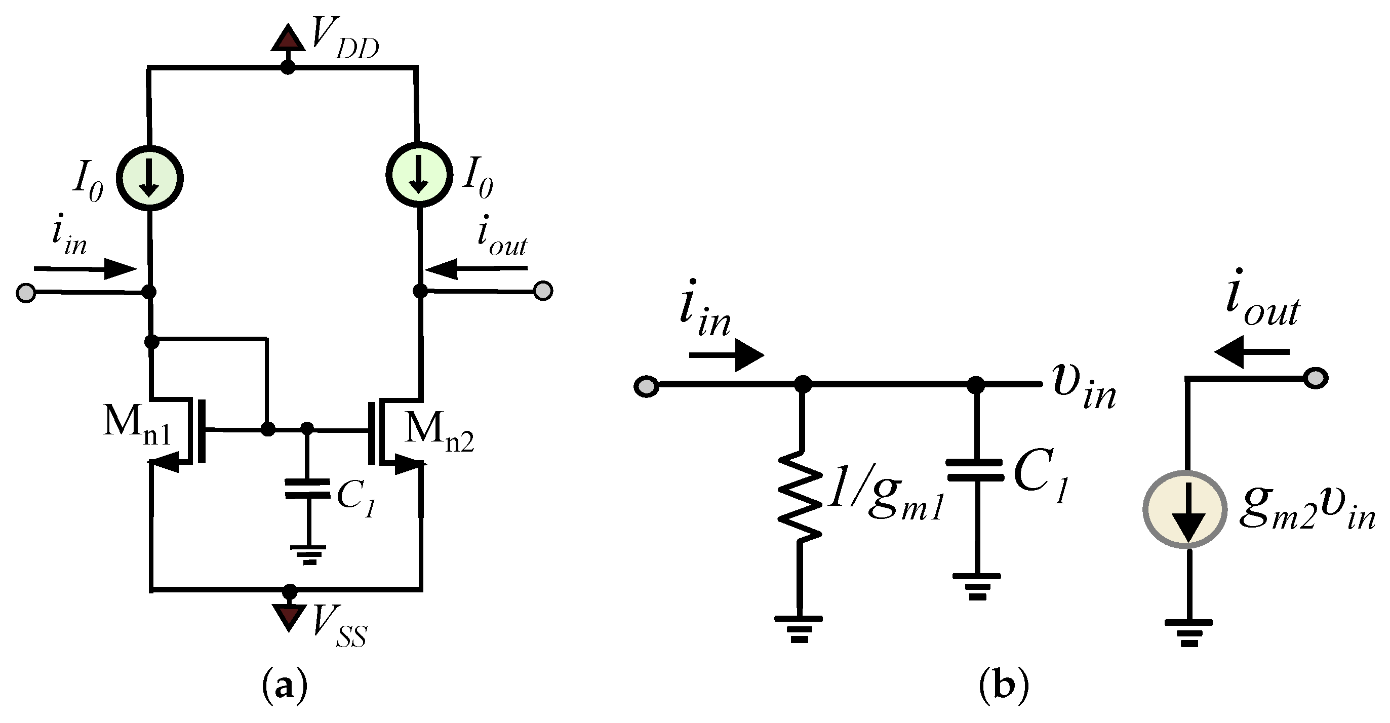
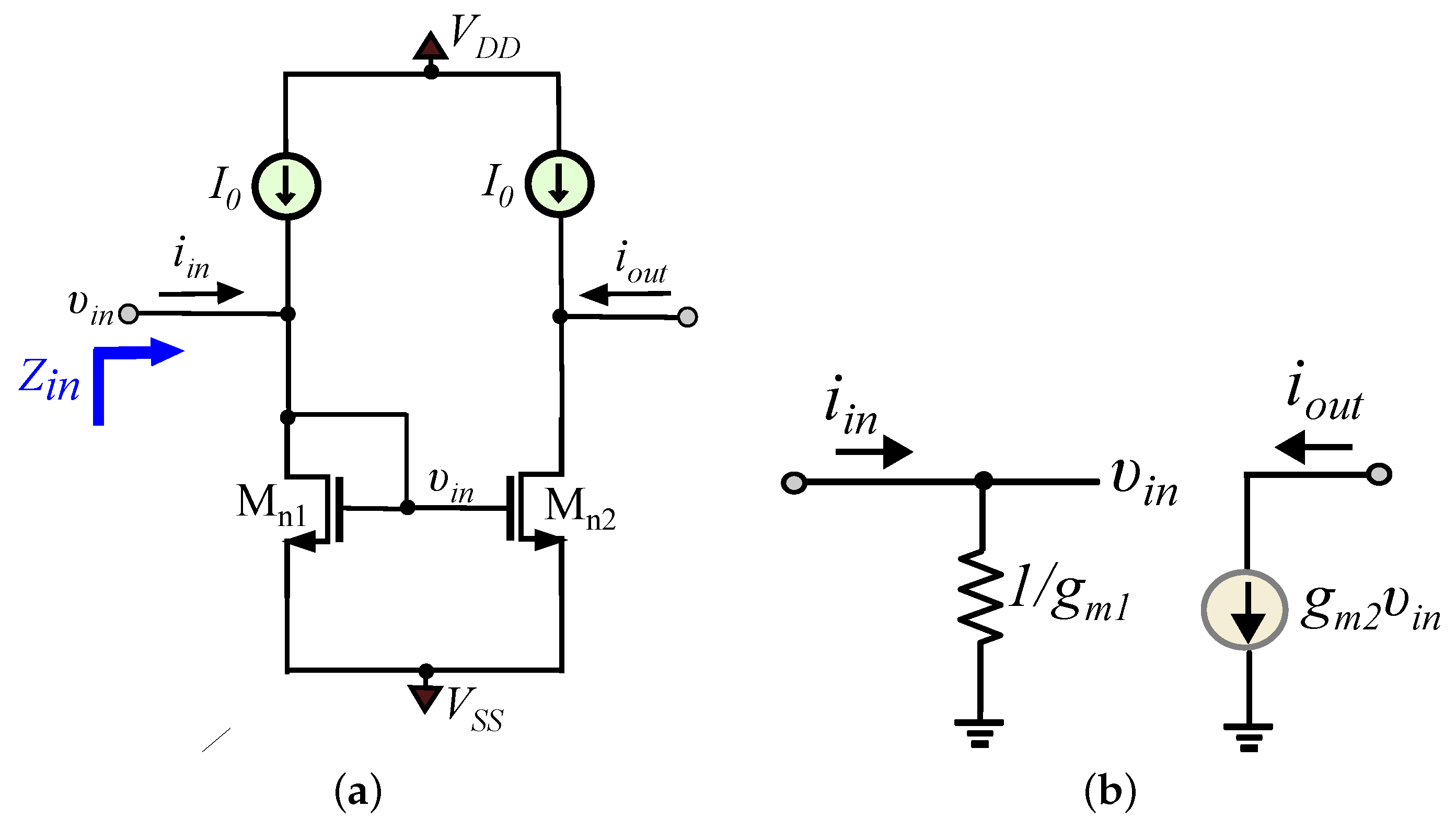
Considering the typical current-mirror structure in Figure 1a, the low-frequency input impedance of this stage ( Z i n ) is equal to 1 / g m 1 , with g m 1 being the small-signal transconductance parameter of the diode-connected transistor Mn1 and neglecting its output impedance [22,23,25,29]. The input current i i n is converted into a voltage υ i n = i · Z i n by transistor Mn1 and this voltage is converted back into a current by transistor Mn2, according to the formula: i o u t = g m 2 υ i n . Assuming that Mn1–Mn2 are matched, the topology acts as a unity gain current-mirror. These operations are described by the small-signal equivalent depicted in Figure 1b.
Figure 1. Basic current-mirror: (a) Circuitry. (b) Small-signal model.
Adding a capacitor C 1 at the input of the stage, as it is shown in Figure 2a, the input impedance becomes: Z i n = ( 1 / g m 1 ) / / ( 1 / C 1 s ) and the structure realizes a lossy integrator (i.e., a first-order unity gain low-pass current transfer function) with cut-off frequency ( ω c ) given by the formula: ω c = g m 1 / C 1 , as it is derived from the small-signal equivalent in Figure 2b [22,23,25].
Figure 2. Lossy integration stage using a current-mirror: (a) Circuitry. (b) Small-signal model [22,23].
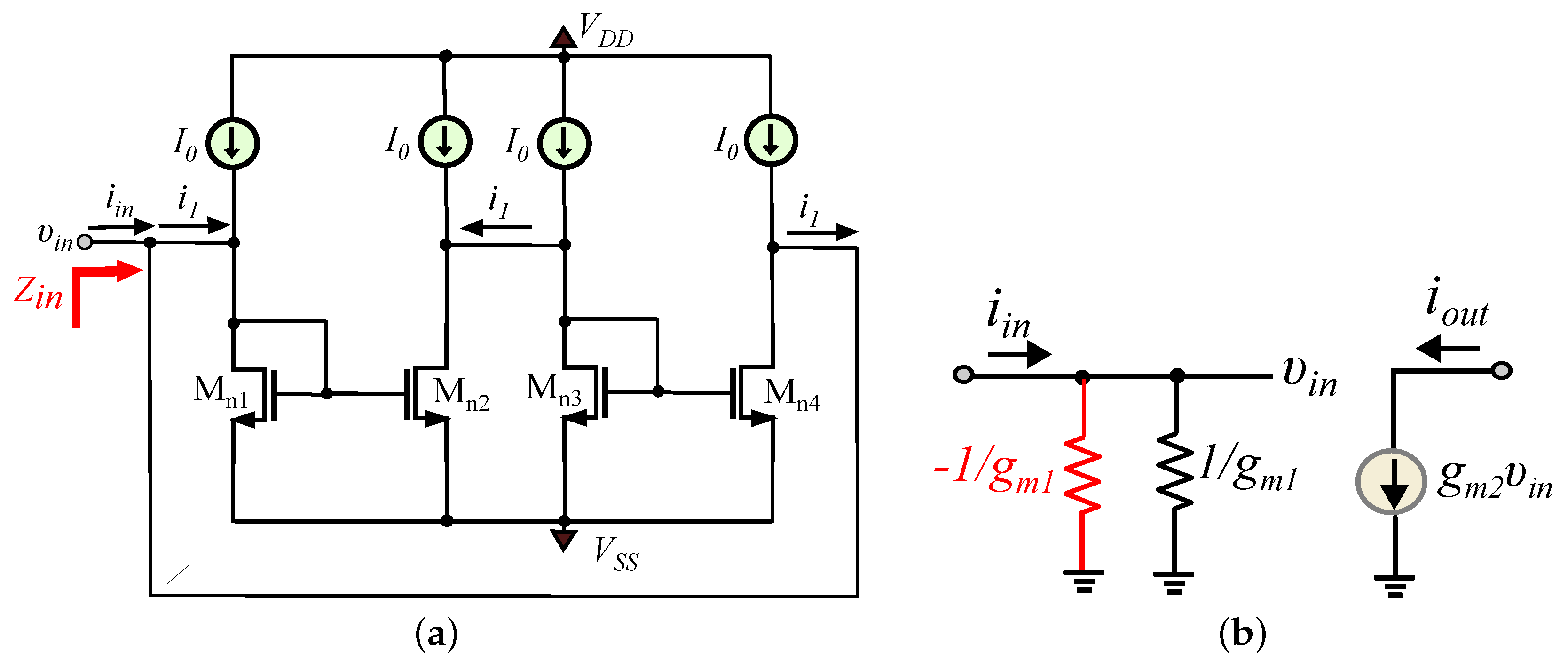
The realization of a lossless integration stage could be performed through the concept presented in Figure 3a,b. Performing a routine analysis in Figure 3a, it is readily obtained that: i i n + i 1 = i 1 ; this condition is only fulfilled for i i n = 0 , making the input impedance to be infinity. In other words, this technique is based on the neutralization of the resistance 1 / g m 1 , by establishing in parallel a negative resistance equal to 1 / g m 1 . This is demonstrated in Figure 3b. It should be noted that the aforementioned transistor-level method is valid only if transistors Mn1–Mn2 and Mn3–Mn4 are matched, i.e., g m 1 = g m 2 and g m 3 = g m 4 .
Figure 3. Neutralization of the impedance 1 / g m 1 of the topology in Figure 1: (a) Circuitry. (b) Small-signal model.
Moreover, the addition of a capacitor C 1 at the input of the stage, as it is shown in Figure 4, makes it to behave as a lossless integration stage with the time-constant given by the formula: τ = C 1 / g m 2 , provided that g m 1 = g m 2 = g m 3 and g m 4 = g m 5 [22,23].
Figure 4. Current-mode lossless integrator stage derived by following the concept in Figure 3 [22,23].
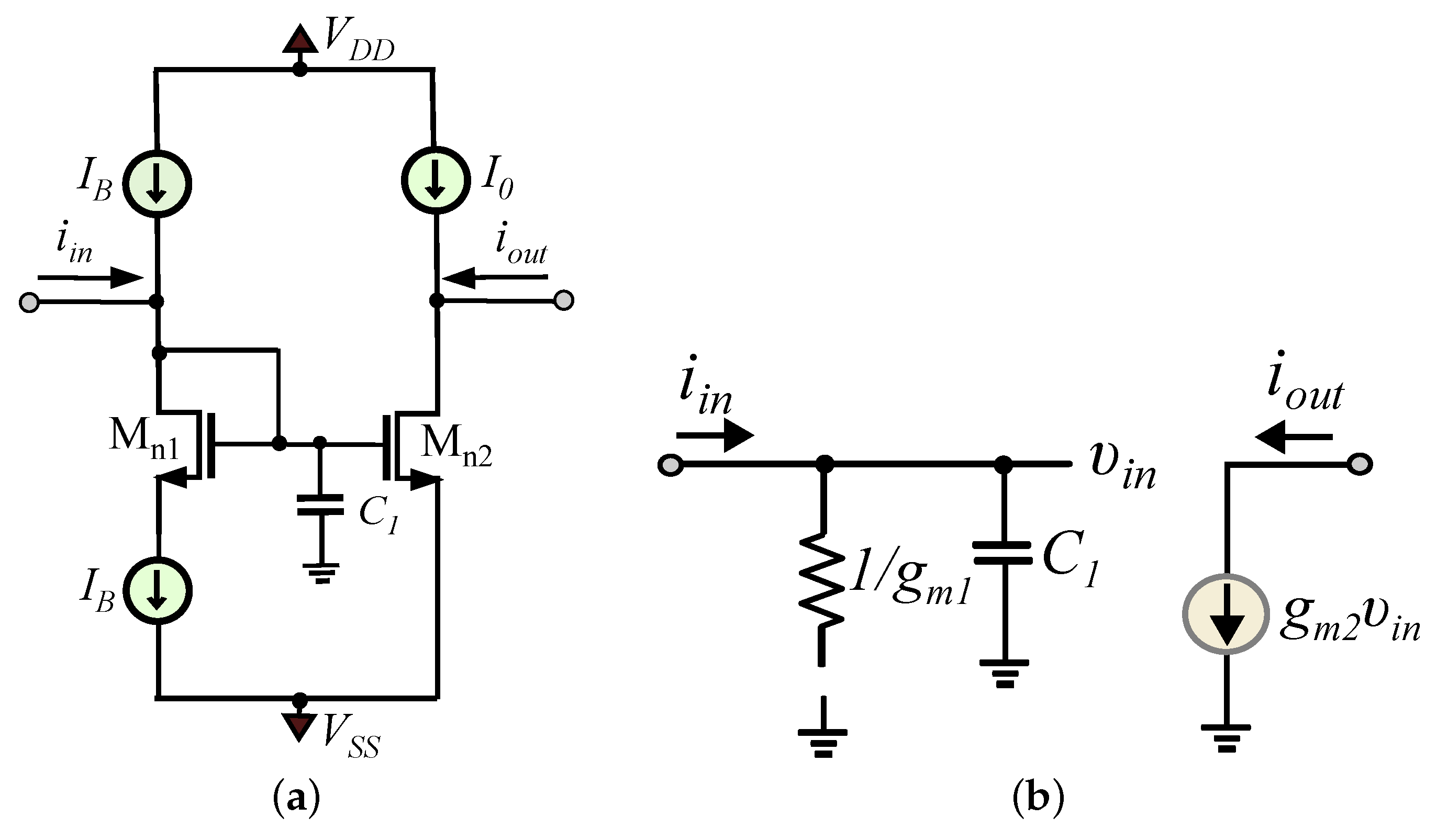
Another way for implementing a lossless integrator is by establishing an open circuit in the path of the resistor 1 / g m 1 . This concept has been introduced in [35] and is demonstrated in Figure 5a. Due to the addition of the extra current source I 0 in the input branch, the current that flows through Mn1 during the small-signal operation is equal to zero and from the equivalent in Figure 5b it is readily derived that the input impedance of the topology becomes equal to 1 / C 1 s , because the resistor 1 / g m 1 is floating.
Figure 5. Lossless integration stage introduced in [35]: (a) Circuitry. (b) Small-signal model.
The input voltage is
υ i n = i i n C 1 s ,
and, taking into account that the output current is given by the formula: i o u t = g m 2 υ i n , the resulting expression of the realized transfer function is
H ( s ) i o u t i i n = 1 ( C 1 / g m 2 ) s ,
making the associated time constant to be
τ = C 1 g m 2 .
Inspecting the topologies in Figure 2, Figure 4 and Figure 5, the following conclusions could be obtained:
(a)
The topology in Figure 5 is derived from that in Figure 2, just by adding an extra current source.
(b)
The component count in the topology in Figure 5 is significantly reduced with regards to that in Figure 4.
(c)
The power dissipation of the integrator in Figure 4 equals to 5 V D D V S S I 0 , while in Figure 5 the dissipation is V D D V S S I B + I 0 .
(d)
There is not any matching requirement between the transistors Mn1 − Mn2, in contrast to the topology in Figure 5. The reason is that, under the assumption that the capacitor is initially discharged, the value of the voltage at the common-gate connection of Mn1 − Mn2 is equal to zero. Therefore, the gate-source voltage of Mn2 becomes equal to V S S , making its transconductance to be: g m 2 = 2 I 0 / V S S offering linear dependence from the current I 0 .
The aspect ratio of Mn1 is chosen in such a way that there will be a suitable headroom voltage, for a given value of I B , available for the operation of the current source which is connected at its source terminal.

3. Proposed Sinusoidal Quadrature Oscillator

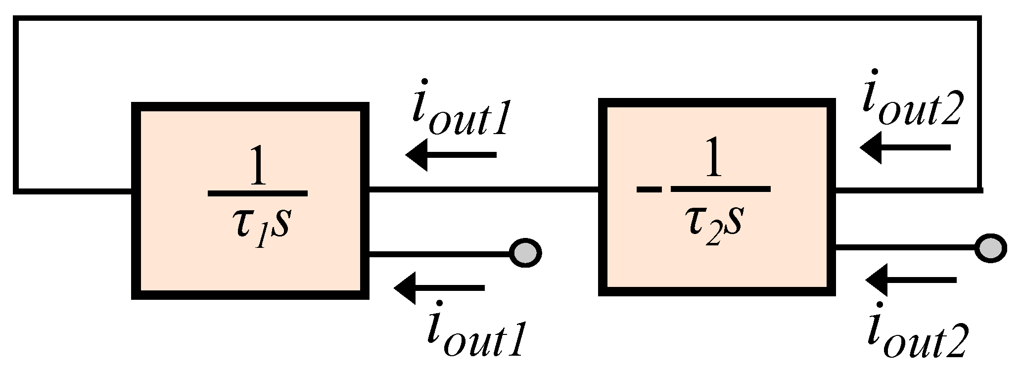
The Functional Block Diagram (FBD) of a current-mode sinusoidal quadrature oscillator, constructed from a two-integrator loop is depicted in Figure 6. As the open-loop gain is given by the formula: L ( s ) = 1 / ( τ 1 τ 2 s 2 ) , it is readily obtained that the topology unconditionally oscillates at frequency ( ω 0 = 2 π f 0 )
f 0 = 1 2 π τ 1 τ 2 .
Figure 6. Functional Block Diagram of a two-integrator loop current-mode quadrature oscillator.
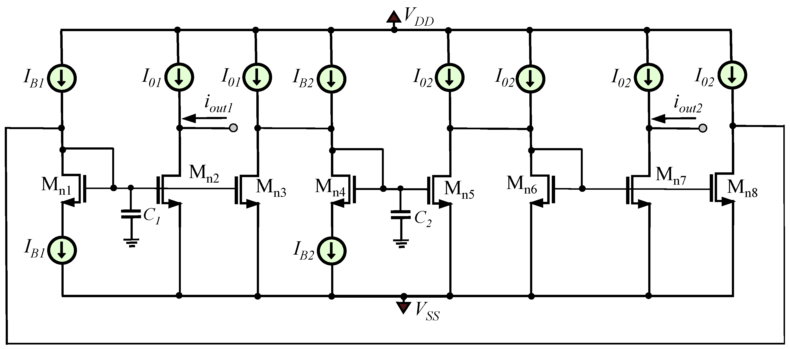
The implementation of the FBD in Figure 6 can be performed using the lossless integration stage presented in Figure 7.
Figure 7. Quadrature oscillator based on the integration stage in Figure 5.
The resulting expression of the oscillation frequency is
f 0 = g m 2 g m 5 2 π C 1 C 2 .
According to the analysis provided in [35], the open-loop gain of the integrator is
L ( s ) = g m 2 g m 5 ( r d s , n / / r d s , p ) 1 ( r d s , n / / r d s , p ) 4 [ ( r d s , n / / r d s , p ) 1 C 1 s + 1 ] · [ ( r d s , n / / r d s , p ) 4 C 2 s + 1 ] ,
with ( r d s , n / / r d s , p ) i ( i = 1 , 4 ) being the output resistances of the MOS transistors which implement the current sources associated with the transistors Mn1 and Mn4, respectively. According to (6), the system behaves as cascade connection of two first-order low-pass filter functions with cut-off frequencies given by the formulas: ω c 1 = 1 / ( r d s , n / / r d s , p ) 1 C 1 and ω c 2 = 1 / ( r d s , n / / r d s , p ) 4 C 2 , respectively. At the high frequency range (i.e., ω > > ω c ) both the intermediate stages behave as pure lossless integrators and, consequently, the designer must take care of realizing accurate current-mirrors [28,30,36,37,38] in order the oscillation frequency to be unaltered.
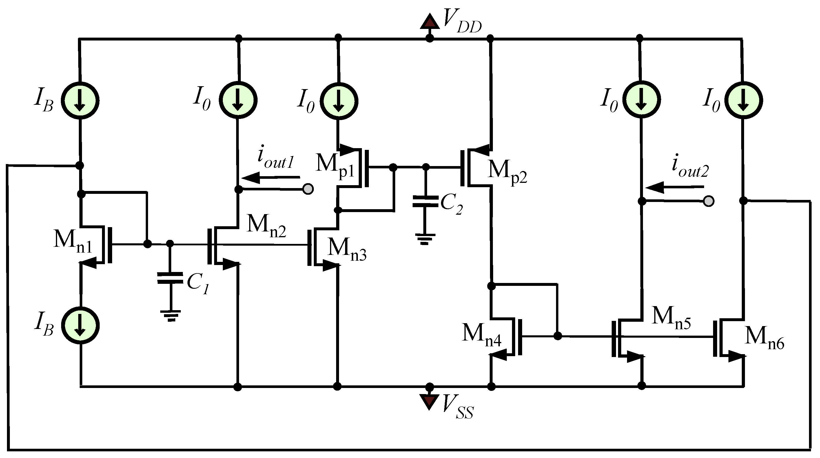
Another possible implementation of the oscillator is that demonstrated in Figure 8, where the core of the second integrator is realized by the pair of Mp1 − Mp2 pMOS transistors. Inspecting the topologies in Figure 7 and Figure 8, it is readily obtained the reduction of the number of the required bias current sources, as 10 are employed in Figure 7 and 6 in Figure 8. The price paid for this achievement is that the maximum frequency of operation is reduced and this is originated from the reduced mobility of the pMOS transistors, with regards to their nMOS transistors.
Figure 8. Simplification of the topology in Figure 7 using a pMOS version of the lossless integrator.
The performance of the realized oscillator is compared with that offered by the corresponding CMOS-based current-mode implementations published in the literature. According to the results provided in Table 1, the presented topologies offer minimization of the circuit complexity with regards to the literature, with that in Figure 8 being the most economical one.
Table 1. Performance comparison results of the lossless oscillators in Figure 7 and Figure 8.

4. Simulation Results

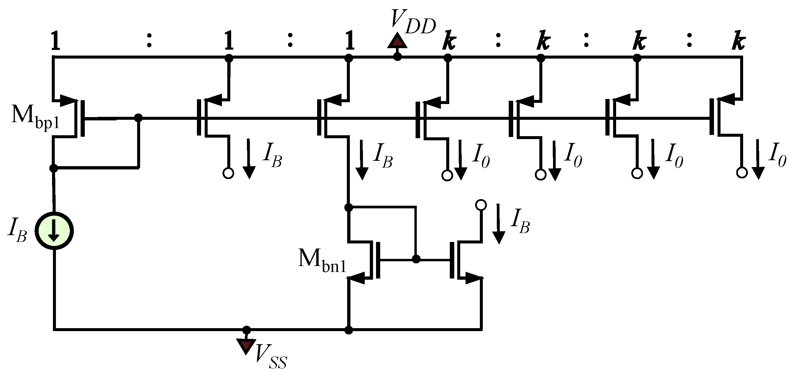
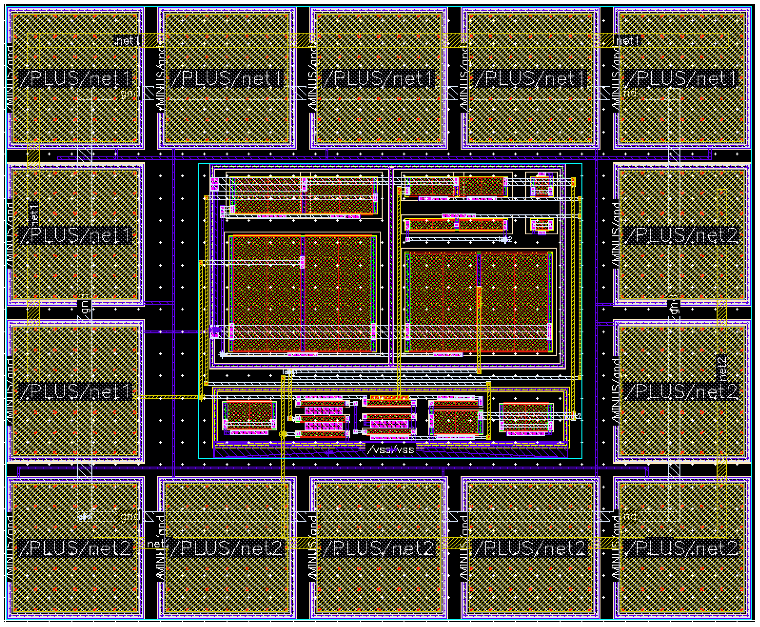
The behavior of the proposed oscillator shown in Figure 8 is analyzed using the Cadence IC design suite with the Design Kit provided by the AMS CMOS 0.35 μm process design kit. The aspect ratios of the nMOS and pMOS transistors Mn1 − Mn6 and Mp1 − Mp2 are 1 μm/10 μm and 4 μm/10 μm, respectively. The circuit operates with a supply voltage of V D D = V S S = 1.5 V, while I B = 1 μA and I 0 = 5.84 μA. The distribution of the dc bias currents I B and I 0 is performed through the utilization of the scheme in Figure 9, where the aspect ratios of Mbn1 and Mbp1 are 1 μm/10 μm and 8 μm/15 μm, respectively, while the scale factor k is equal to I 0 / I B . The capacitances are set to C 1 = C 2 = 7.43 pF in order to achieve an oscillation frequency of 250 kHz. The layout design of the topology in Figure 8 is depicted in Figure 10, with the dimensions being 168 μm × 138 μm.
Figure 9. Circuitry for generating the dc bias currents I B and I 0 ( k = I 0 / I B ).
Figure 10. Layout design of the oscillator in Figure 8.
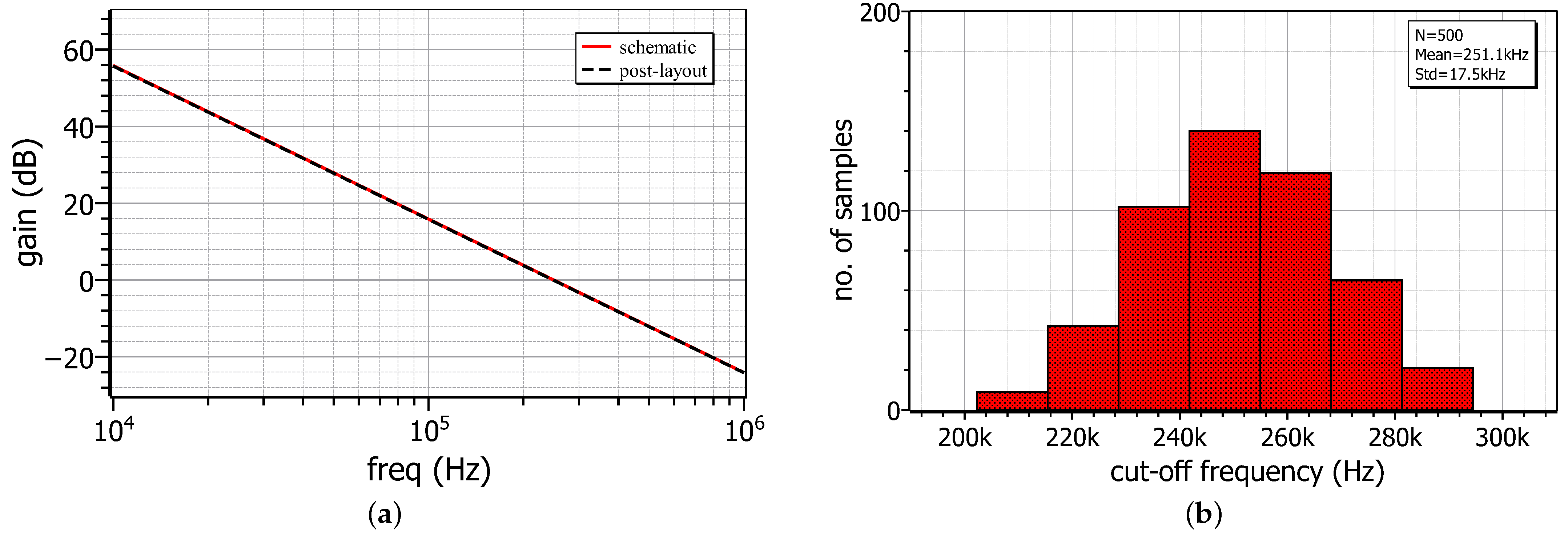
Considering the open-loop configuration of the oscillator, its gain response is depicted in Figure 11a with the simulated value of the unity-gain frequency (which is also the oscillation frequency) being equal to 251.1 kHz. The sensitivity performance of the proposed oscillator is evaluated using the Monte-Carlo analysis tool, for N = 500 runs. The resulting statistical histogram of the open-loop unity-gain frequency is given in Figure 11b, where the value of the standard deviation, derived by considering the effects of both the process parameters variation and MOS transistors parameters mismatching, is 17.5 kHz. As the mean value is 251.1 kHz, it is concluded that the oscillator has reasonable sensitivity characteristics.
Figure 11. Post-layout frequency-domain behavior of the oscillator: (a) Open-loop gain response. (b) Monte-Carlo analysis results of the open-loop unity-gain frequency.
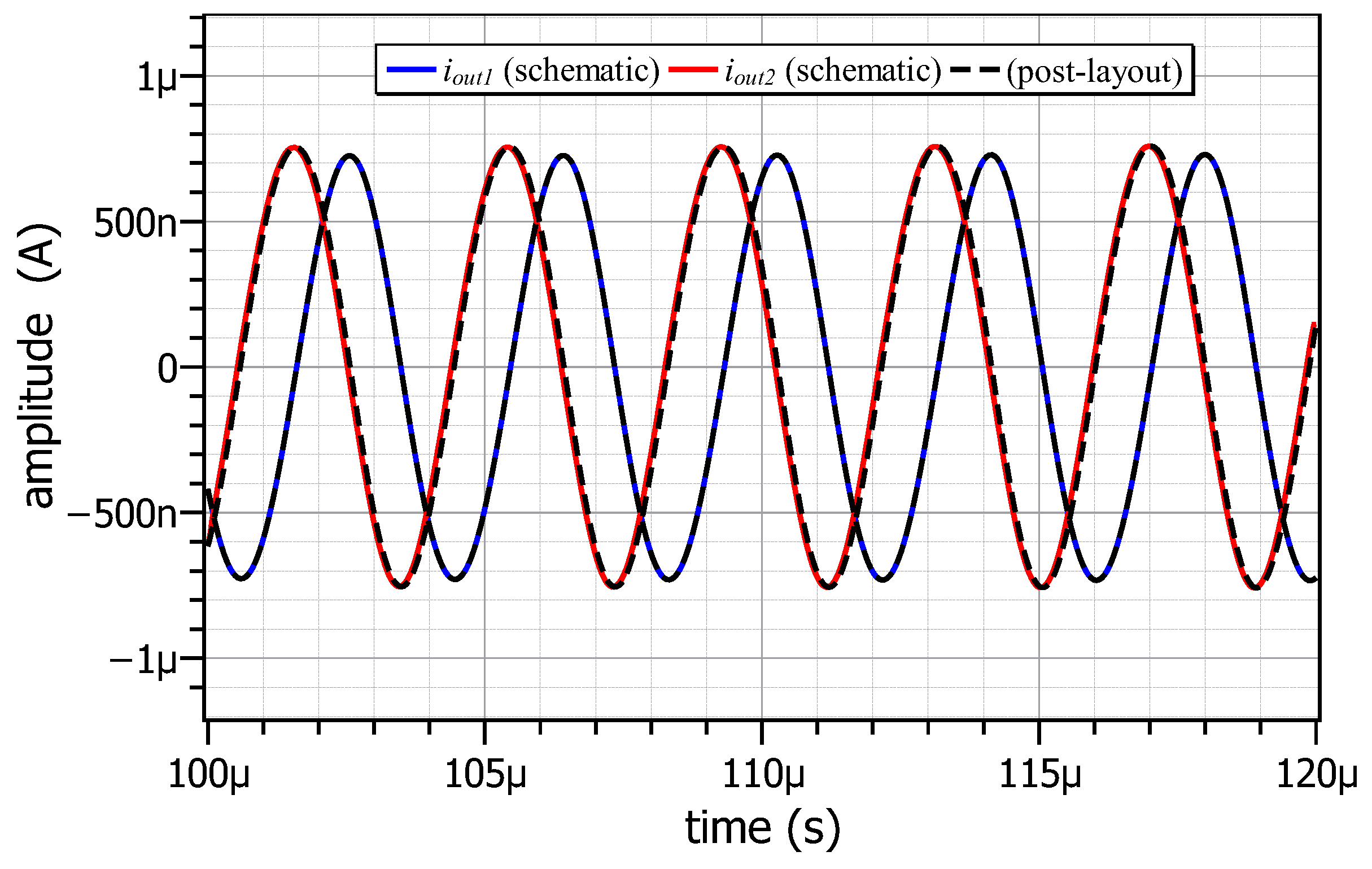
The time-domain post-layout results of the current outputs are given in Figure 12, where the oscillation frequency and the phase difference between the outputs being 251.1 kHz and 87.1°, close to the theoretical values 250 kHz and 90°, respectively.
Figure 12. Post-layout time-domain simulated output waveforms of the oscillator.
The Total Harmonic Distortion (THD) is measured equal to 3.78% for the first output and 4% for the second one, using Periodic Steady-State (PSS) analysis offered by the IC design Cadence suite.
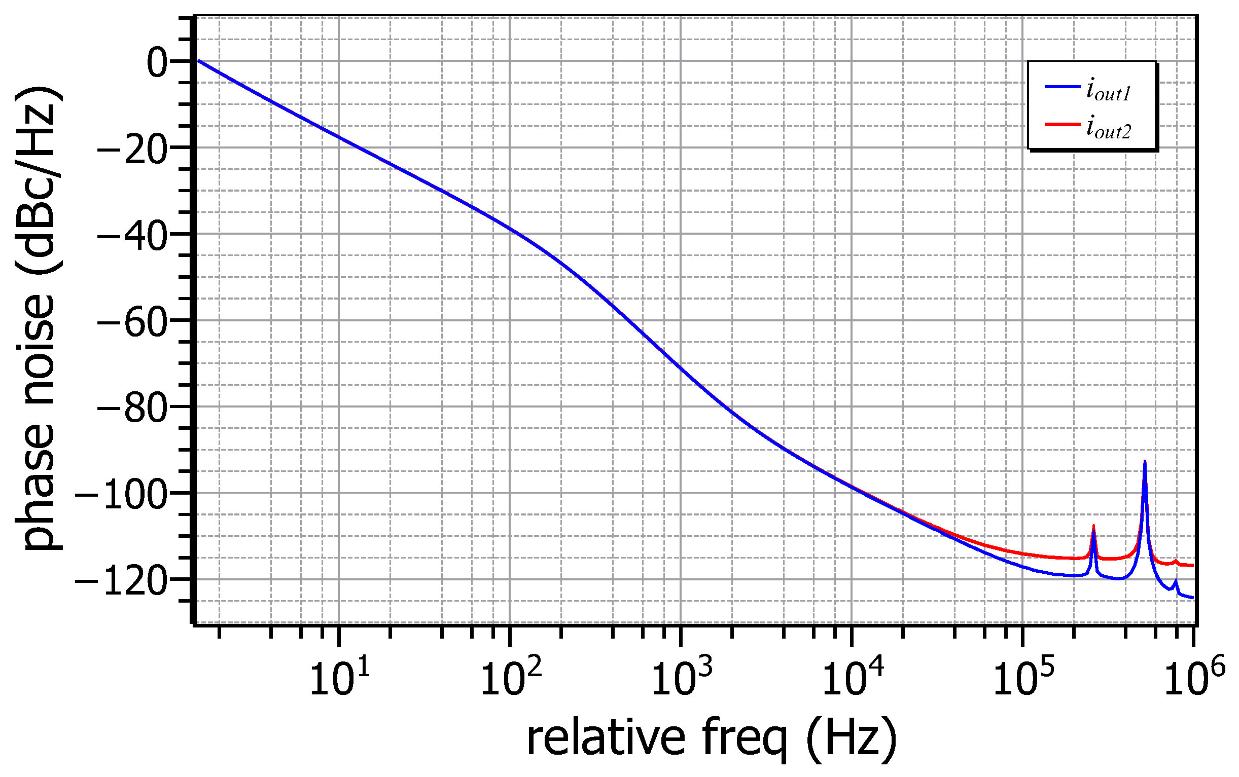
As next step, the phase noise of both outputs is evaluated and the resulting plots are provided in Figure 13. The values of the spot phase noise at 2 f 0 and 3 f 0 are 3.44 pA/ Hz and 22.89 pA/ Hz for i o u t 1 and 4.19 pA/ Hz and 23.51 pA/ Hz for i o u t 2 , respectively.
Figure 13. Phase noise plots of the outputs of the proposed oscillator.

5. Conclusions

The presented oscillator topology offers significant reduction of the required circuit complexity, with regards to the literature. This is achieved through the realization of a slightly modified version of the simple lossy integration stage, avoiding the conventional way where an extra feedback path must be added for neutralizing the small-signal equivalent resistance of diode connected transistor. The layout design of the presented topology is demonstrated and the obtained post-layout simulation results in both frequency and time-domain confirm that the scheme has reasonable performance in terms of accuracy, sensitivity, and linearity. Consequently, it is an attractive candidate for implementing analog signal processing systems, where the demand of reduced low power dissipation is crucial.

Author Contributions

Conceptualization, C.P. and S.M.; methodology, C.P. and J.N.; software, J.N.; validation, J.N.; formal analysis, C.P. and J.N.; investigation, J.N.; writing—original draft preparation, J.N. and C.P.; writing—review and editing, J.N., C.P. and S.M.; supervision, C.P. and S.M. All authors have read and agreed to the published version of the manuscript.

Funding

This research received no external funding.

Institutional Review Board Statement

Not applicable.

Data Availability Statement

The original contributions presented in this study are included in the article. Further inquiries can be directed to the corresponding author(s).

Acknowledgments

The research work was supported by the Hellenic Foundation for Research and Innovation (HFRI) under the 5th Call for HFRI PhD Fellowships (Fellowship Number: 19286).

Conflicts of Interest

The authors declare no conflicts of interest.

References

  1. Siripruchyanun, M.; Jaikla, W. Cascadable current-mode biquad filter and quadrature oscillator using DO-CCCIIs and OTA. Circuits Syst. Signal Process. 2009, 28, 99–110. [Google Scholar] [CrossRef]
  2. Thosdeekoraphat, T.; Summart, S.; Saetiaw, C.; Santalunai, S.; Thongsopa, C. CCTAs based current-mode quadrature oscillator with high output impedances. Int. J. Electron. Electr. Eng. 2013, 1, 52–56. [Google Scholar] [CrossRef]
  3. Sakul, C.; Jaikla, W.; Dejhan, K. New resistorless current-mode quadrature oscillators using 2 CCCDTAs and grounded capacitors. Radioengineering 2011, 20, 890–896. [Google Scholar]
  4. Keawon, R.; Jaikla, W. A resistor-less current-mode quadrature sinusoidal oscillator employing single CCCDTA and grounded capacitors. Prz. Elektrotechniczny 2011, 87, 138–141. [Google Scholar]
  5. Summart, S.; Thongsopa, C.; Jaikla, W. OTA based current-mode sinusoidal quadrature oscillator with non-interactive control. Prz. Elektrotechniczny 2012, 88, 14–17. [Google Scholar]
  6. Maiti, S.; Pal, R.R. Dual-mode quadrature oscillator employing single Current Controlled Current Conveyor transconductance amplifier. Int. J. Innov. Res. Sci. Eng. Technol. 2013, 2, 3105–3112. [Google Scholar]
  7. Thosdeekoraphat, T.; Summart, S.; Thongsopa, C. Current-mode Sinusoidal Oscillator using Single Dual-output Current Controlled Current Conveyor Transconductance Amplifier (DO-CCCCTA). Aust. J. Basic Appl. Sci 2013, 7, 230–236. [Google Scholar]
  8. Siriphot, D.; Pookrongtong, N.; Lumchanao, W. Single CDCTA Based Electronically Adjustable Current-mode Quadrature Sinusoidal Oscillator. Appl. Sci. Eng. Prog. 2018, 11, 209–216. [Google Scholar] [CrossRef][Green Version]
  9. Kumngern, M.; Jongchanachavawat, W.; Phatsornsiri, P.; Wongprommoon, N.; Khateb, F.; Kulej, T. Current-mode first-order versatile filter using translinear current conveyors with controlled current gain. Electronics 2023, 12, 2828. [Google Scholar] [CrossRef]
  10. Kumngern, M.; Khateb, F.; Kulej, T. A Novel Multiple-Input Single-Output Current-Mode Shadow Filter and Shadow Oscillator Using Current-Controlled Current Conveyors. Circuits Syst. Signal Process. 2024, 43, 5438–5462. [Google Scholar] [CrossRef]
  11. Souliotis, G.; Psychalinos, C. Harmonic oscillators realized using current amplifiers and grounded capacitors. Int. J. Circuit Theory Appl. 2007, 35, 165–173. [Google Scholar] [CrossRef]
  12. Jantakun, A.; Jaikla, W. Current-mode quadrature oscillator based on CCCDTAs with noninteractive dual-current control for both condition of oscillation and frequency of oscillation. Turk. J. Electr. Eng. Comput. Sci. 2013, 21, 81–89. [Google Scholar] [CrossRef]
  13. Summart, S.; Thongsopa, C.; Jaikla, W. New current-controlled current-mode sinusoidal quadrature oscillators using CDTAs. AEU-Int. J. Electron. Commun. 2015, 69, 62–68. [Google Scholar] [CrossRef]
  14. Das, R.; Bhowmick, B.; Paul, P.; Karmakar, S.; Banerjee, K. Current Differencing Transconductance Amplifier (CDTA) based current mode quadrature oscillator. In Advances in Computer, Communication and Control: Proceedings of ETES 2018; Springer: Singapore, 2019; pp. 35–47. [Google Scholar] [CrossRef]
  15. Yeşil, A.; Kaçar, F. Current and voltage mode quadrature oscillator based on Voltage Differencing Buffered Amplifier. Electrica 2018, 18, 6–12. [Google Scholar] [CrossRef]
  16. Singh, A.K.; Kumar, P.; Senani, R. Current-mode quadrature oscillator using CFCC. Am. J. Electr. Electron. Eng. 2018, 6, 85–89. [Google Scholar]
  17. Kumngern, M.; Khateb, F. Current-mode universal filter and quadrature oscillator using Current Controlled Current Follower Transconductance Amplifiers. Analog Integr. Circuits Signal Process. 2019, 100, 235–248. [Google Scholar] [CrossRef]
  18. Gupta, M.; Dogra, P.; Arora, T.S. Novel current mode universal filter and dual-mode quadrature oscillator using VDCC and all grounded passive elements. Aust. J. Electr. Electron. Eng. 2019, 16, 220–236. [Google Scholar] [CrossRef]
  19. Arora, T.S.; Gupta, M.; Gupta, S.N. An Explicit Output Current-mode Quadrature Sinusoidal Oscillator and a Universal Filter Employing Only Grounded Passive Components-a Minimal Realisation. Adv. Electr. Electron. Eng. 2021, 19, 258–271. [Google Scholar] [CrossRef]
  20. Roongmuanpha, N.; Tangsrirat, W.; Pukkalanun, T. Single VDGA-based mixed-mode universal filter and dual-mode quadrature oscillator. Sensors 2022, 22, 5303. [Google Scholar] [CrossRef]
  21. Summart, S.; Sirithai, S.; Vaisopha, B.; Jantakun, A. Electronically controlled biquadratic filter and quadrature oscillator using CDTAs. Int. J. Eng. Technol. Innov. 2022, 12, 322–335. [Google Scholar] [CrossRef]
  22. Ramirez-Angulo, J.; Róbinson, M.; Sanchez-Sinecio, E. Current-mode continuous-time filters: Two design approaches. IEEE Trans. Circuits Syst. II Analog Digit. Signal Process. 1992, 39, 337–341. [Google Scholar] [CrossRef]
  23. Lee, S.S.; Zele, R.H.; Allstot, D.J.; Liang, G. CMOS continuous-time current-mode filters for high-frequency applications. IEEE J. Solid-State Circuits 1993, 28, 323–329. [Google Scholar] [CrossRef]
  24. Koliopoulos, C.; Psychalinos, C. A comparative study of the performance of the flipped voltage follower based low-voltage current mirrors. In Proceedings of the 2007 International Symposium on Signals, Circuits and Systems, Iasi, Romania, 13–14 July 2007; pp. 192–195. [Google Scholar] [CrossRef]
  25. Souliotis, G.; Haritantis, I. Current-mode filters based on current mirror arrays. Int. J. Circuit Theory Appl. 2008, 36, 173–183. [Google Scholar] [CrossRef]
  26. Laoudias, C.; Psychalinos, C. Universal biquad filter topology using low-voltage current mirrors. Int. J. Circuit Theory Appl. 2012, 40, 65–75. [Google Scholar] [CrossRef]
  27. Laoudias, C.; Psychalinos, C. 1.5-V complex filters using current mirrors. IEEE Trans. Circuits Syst. II Express Briefs 2011, 58, 575–579. [Google Scholar] [CrossRef]
  28. Gupta, M.; Aggarwal, P.; Singh, P.; Jindal, N.K. Low voltage current mirrors with enhanced bandwidth. Analog Integr. Circuits Signal Process. 2009, 59, 97–103. [Google Scholar] [CrossRef]
  29. Aggarwal, B.; Gupta, M.; Gupta, A.K. A comparative study of various current mirror configurations: Topologies and characteristics. Microelectron. J. 2016, 53, 134–155. [Google Scholar] [CrossRef]
  30. Shrivastava, A.; Pandey, R.; Jindal, C. Low-voltage flipped voltage follower cell based current mirrors for high frequency applications. Wirel. Pers. Commun. 2020, 111, 143–161. [Google Scholar] [CrossRef]
  31. Aggarwal, B. Novel current mirrors based on folded flipped voltage follower configuration. Wirel. Pers. Commun. 2022, 123, 645–653. [Google Scholar] [CrossRef]
  32. Kumar, A.; Tripathi, S.L.; Verma, C.; Raboaca, M.S.; Enescu, F.M.; Mihaltan, T.C. Design and Analysis of Low Power Bio-amplifier with Current Mirror Topology at CMOS 45nm Technology Node. In Proceedings of the 2022 14th International Conference on Electronics, Computers and Artificial Intelligence (ECAI), Ploiesti, Romania, 30 June–1 July 2022; pp. 1–5. [Google Scholar] [CrossRef]
  33. Huang, J.; Wang, C.; Zhou, T.; Lu, W.; Zhao, Y.; Liu, Y.; Li, Y. A shifting current mirror driver circuit for electrical impedance tomography applications. IEEE Trans. Circuits Syst. II Express Briefs 2023, 70, 3832–3836. [Google Scholar] [CrossRef]
  34. Nam, K.; Choi, G.; Yoo, M.; Kang, S.; Jin, B.; Son, H.; Kim, K.; Ko, H. A low-noise and mismatch-tolerant current-mirror-based potentiostat circuit for glucose monitoring. Microelectron. J. 2023, 132, 105694. [Google Scholar] [CrossRef]
  35. Nako, J.; Psychalinos, C.; Minaei, S.; Yuce, E. Current-Mirror Based Filters with Reduced Circuit Complexity. Int. J. Circuit Theory Appl. 2025. early view. [Google Scholar] [CrossRef]
  36. Doreyatim, M.; Akbari, M.; Nazari, M.; Mahani, S. A low-voltage gain boosting-based current mirror with high input/output dynamic range. Microelectron. J. 2019, 90, 88–95. [Google Scholar] [CrossRef]
  37. Monfaredi, K.; Faraji Baghtash, H. An extremely low-voltage and high-compliance current mirror. Circuits Syst. Signal Process. 2020, 39, 30–53. [Google Scholar] [CrossRef]
  38. Jindal, C.; Pandey, R. A high output resistance, wide bandwidth, and low input resistance current mirror using flipped voltage follower cell. Int. J. Circuit Theory Appl. 2021, 49, 3286–3301. [Google Scholar] [CrossRef]
Disclaimer/Publisher’s Note: The statements, opinions and data contained in all publications are solely those of the individual author(s) and contributor(s) and not of MDPI and/or the editor(s). MDPI and/or the editor(s) disclaim responsibility for any injury to people or property resulting from any ideas, methods, instructions or products referred to in the content.

Article Metrics

Citations

Article Access Statistics

Multiple requests from the same IP address are counted as one view.