Abstract
Voltage stacking is a technique in which multiple integrated circuits are stacked in series between the supply voltage instead of in parallel, thus improving the energy efficiency of the power distribution network. Unfortunately, voltage stacking presents stability challenges for integrated circuits within the stack. A first-order model to quantify variability, stability, and power metrics for an array of voltage-stacked asynchronous integrated circuits is presented. Voltage variability and power consumption are accounted for and discussed. Limitations of the model are identified outside of the nominal behavior. The number of columns in the architecture, chip leakage, and supply voltage are shown to be the key contributors to the stability, performance, and energy efficiency of a system of voltage-stacked asynchronous processors. A higher leakage to active power ratio, though usually avoided by chip designers, is shown to improve stability and be key in designing stacks without external balancing. Outputs of the model enable system and chip designers to evaluate first-order trade-offs in energy efficiency, performance, and system cost. These fundamental data allow designers to make informed design and optimization trade-offs between asynchronous voltage-stacked architectures and the integrated circuits used therein. Analysis of this model shows that various voltage-stacked configurations, such as one with a 48 V supply using 100 rows and 11 columns, can be designed with less than 10% voltage variation per chip, mitigating the need for external voltage balancing.
Keywords:
voltage stacking; digital design; SoC; NoC; energy efficient; power delivery system; asynchronous 1. Introduction
Power efficiency in modern integrated circuits (ICs) is a primary figure of merit due to the increase in power density and energy impacts from our increasingly electronically connected world. The energy consumption of a compute-intensive system comes from three primary sources: the ICs, the power delivery, and thermal management. These systems work in concert to produce a system with a particular energy, performance, and cost footprint. Various methods exist to improve the energy footprint of a system. Approaches such as low power circuit design and power gating reduce energy consumption in an IC. Phase change, immersion cooling, and various thermal interface materials affect the efficiency of the thermal management of a system. Dynamic voltage scaling and voltage stacking are methods that improve chip efficiency and the power delivery of a system.
Reducing supply voltage is one of the best methods to reduce the overall power consumption of an IC application that is not compute-limited due to abundant concurrency [1]. As the supply voltage is reduced from the nominal voltage, both performance and energy consumption per operation are reduced. The reduced performance per computation is offset by increased concurrency. Thus, one can produce a system that exhibits the same computation rate at a significantly reduced energy per computation by reducing voltage and adding computing cores. Delivering a stable low-loss supply at low voltages to these systems is challenging. DC conversion to the near-threshold voltages of today’s FinFET ICs requires expensive modern components. Conversion efficiency drops towards 80% at near-threshold voltages. These systems also suffer substantial loss and supply noise due to high supply current, particularly under variation in demand.
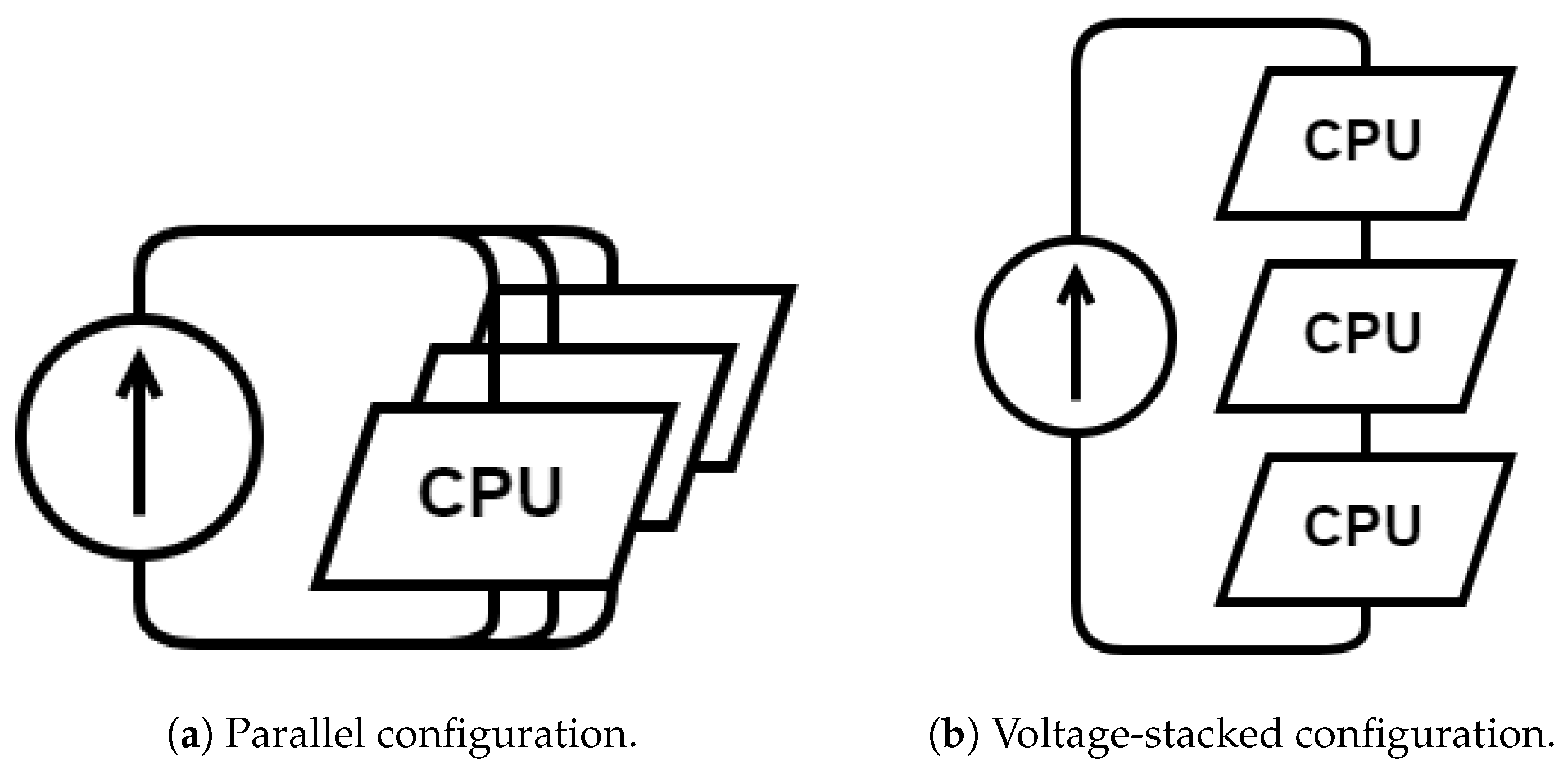
This paper focuses on an approach to design power delivery that reduces system cost and energy consumption by supplying ICs with near threshold voltage using a voltage-stacked (VS) chip configuration. Since VS is novel for most designers, this paper offers tools for both chip and printed circuit board (PCB) designers to efficiently communicate and achieve the desired architecture. Chip and board architectures are typically performed independently. Conversely, the models developed here show that optimizing a VS system requires IC/PCB co-design. This co-design directly affects system optimization including cost, PCB size, thermals, external component selection, and software control. For instance, consider the size of the PCB(s) for a VS system. A chip designer may want to design a small chip that would result in a 100 × 50 structure. This would lead to large PC boards with complicated routing and power delivery. Power delivery cost, efficiency, and noise can all be improved by employing a “stacked power delivery” method [2]. Rather than a low voltage and high current supply provided in a parallel configuration, shown in Figure 1a, high voltage and low current are supplied to a series stack of processors, as shown in Figure 1b. This results in more efficient and stable DC conversion because it is performed at higher voltages. Using Kirchhoff’s Current Law, a single path leads to the same current circulating through all the ICs stacked on top of one another. Thus, the current is divided by the number of series IC layers.

Figure 1.
Difference between traditional power supply and voltage stacking, showing three IC layers.
Higher DC voltage supplies also allow a conversion step to be skipped. Assume AC to be converted to a 12 V DC supply. This 12 V supply can be directly provided to a stack of 30 ICs to produce an average supply of 400 mV per chip. This removes the need to perform DC-to-DC conversion from 12 V to 400 mV and its associated costs and losses. In this configuration with 30 processors in series, the supply current is 1/30th of the parallel configuration. Thus, the average voltage per chip is and the current is for a supply voltage of with m processors in series.
The effective resistance (and, thus, the voltage at a relative constant current) of each layer in the stack will vary due to the computation load performed at each layer and the process variation that exists within each IC in the stack. If the voltage for any layer is too high, the ICs in that layer will be damaged. A voltage that is too low will result in untimely results. The model developed here reveals that the corner cases are primarily impacted by the properties of the ICs and the topology of the stack. Worst-case conditions can be mitigated by additional electronic components employed on boards and in the ICs, as well as by controlling the computation load in each stack layer.
When the processors are designed using asynchronous design methodologies, variation in voltage supplied to each layer will not impact correct operation (provided it remains within a safe range). The performance and energy consumption will dynamically adjust to the voltage supplied to each processor in the stack. As supply voltage increases, performance and energy consumption increase, reducing the effective resistance of this layer. This results in negative feedback; as the resistance of a layer drops, the voltage supplied to that layer will be reduced. Thus, the fundamental design challenge in implementing a reliable voltage-stacked system of asynchronous processors is to ensure that every layer in the stack maintains its voltage within a safe range.
Asynchronous processors are assumed in the model and evaluation presented here since they are resilient to variation. This capability enables a first-order model using resistors to sufficiently characterize the corner behaviors in a voltage-stacked system. Such an approach does not apply to clocked circuits. In the case of clocked circuits, a change in the supply voltage requires an immediate commensurate modification to the clock frequency for the chips to operate reliably and efficiently.
This paper addresses the fundamental challenge of designing voltage-stacked systems by developing a first-order model and evaluating the worst-case conditions. The model supports leakage and performance due to transistor device thresholds and supply voltages, as well as joint serial and parallel chip configurations where multiple dies or processors can be placed in each layer. Thus, the baseline worst case can be explored for various design and stack parameters, from which mitigation can then be applied. This allows a designer to make trade-offs between the overall topology configuration, device threshold, and mitigation approaches employed.
The models in this paper are general to any technology node or circuit style, with the restriction that the processors are asynchronous. Valid chip and process technology parameters, as well as architectural requirements, must be provided to the models to produce meaningful results. These models will help designers and architects derive parameters that optimize system power, performance, and robustness based on the parameters.
This paper does not address any of the other fundamental challenges in a voltage-stacked system, including the universe of voltage variation mitigation approaches or communication methods between layers to and from ICs in the voltage stack.
2. Previous Work
Kirchhoff’s current law forces each layer in the stack to have a specific aggregate voltage and power consumption based on its effective resistance. The voltage and power for each layer vary based on its relation to other layers in the stack. In a perfectly homogeneous application, all layers have the same voltage and power consumption. Any mismatch in the power consumption of a layer will generate variation in the effective resistance of the layer, which generates a change in voltage at every layer. The relationship produces negative feedback for each layer. If the performance and power consumption of a layer increase, the effective resistance decreases, resulting in a lower supply voltage to this layer. This, in turn, reduces the performance and resistance of that layer. In the case of a heterogeneous application, the voltage across each layer might be different but the core concept is the same. The voltage differences correspond to the difference between the effective resistances of each layer of the stack.
VS has been applied to at least three application spaces. Parallel processing of similar applications through a serially connected stack is the most predominant. Heterogeneous and multi-mode applications have been shown to decrease leakage using a stack. Three-dimensional ICs (3D-ICs) face challenges on their supply lines, and VS provides a novel solution exploiting the already stacked nature of their supplies. Finally, dynamic voltage scaling (DVS) provides an example of an energy-saving technique that could be applied using VS of chips.
Most of the related work implements small systems and provides examples of trade-offs in the architecture of stacked power supplies. We are not aware of any work that provides a general mathematical framework for evaluating the variation and corner cases that exist for a broad range of configurations and chip device threshold choices, as is provided by this work.
2.1. Parallel Processing
VS is motivated by the desire to reduce or eliminate off-chip DC converters with respect to cost, board area, and conversion losses. Pioneering work lays the foundation for what is to be expected with any stacked system by using two or three stacks [2,3]. Early work implemented architectures with a single IC per layer. Later work stacks four 12 V motherboards in a server slice to reach the soft limit of 48 V used by many data centers [4]. By combining the board and chip level concepts, one could see either more ICs in parallel per slice or an architecture where there is a single chip per slice but multiple parallel boards.
Increasing the width of the stack increases robustness by reducing the variation seen between layers in the stack [5,6,7]. A 3 × 3 system and 4 × 4 system are evaluated, which show that one of the ways in which variation can be reduced in the system is to design a system that is wider instead of taller. By doing so, the workload is shared between different cores, and each of them averages out the error, leading to less extreme variation.
Compensation systems to further mitigate the voltage variation between layers have been developed [8,9,10]. Voltage regulators can be employed when the current required for the system is high [8]. A 20× lower voltage drop has been obtained with a 4 × 4 voltage-stacked system when the regulator is on versus off. Compensation systems have also been shown to reduce 61.5% of the power delivery subsystems as well as achieve 92.3% of system-level power delivery efficiency [9].
2.2. Heterogeneous and Multi-Mode Applications
Heterogeneous and multi-mode applications are grouped together since the objective in both cases is to reduce leakage. In the case of multi-mode, leakage is mitigated by switching between one or more active modes and idle [11,12,13]. In another application, memories are voltage stacked. When a memory chip idles, the supply node existing between the memories is swapped for the VDD of one side and the GND of the other. Voltage scaling is also applied to the stack. A heterogeneous stack with two layers at 0.4 V and the memory layer at 0.9 V for a total of 1.7 V has been successfully implemented [14]. Variation in the body-bias voltage is used to balance the current. This work is compared to a traditional design that requires an LDO to perform DC conversion from 0.9 V to 0.4 V. A 1.6× efficiency compared to the parallel implementation is reported [14].
2.3. 3D-ICs
VS has also been shown to be a solution to power distribution in 3D-ICs [15,16,17,18]. The computation density increases the voltage noise and electromigration, which results in failures either in timing or in damage to the chip. VS is proposed as a solution that would permit charges to be recycled and, thus, divide the amount of current required by the system. One study shows that DC noise in the supply becomes the main concern rather than AC while using this voltage-stacking technique [17]. However, they also show a noise reduction of 25–45% and a reduction of 37–63% of the power used in the supply. Another study shows the noise being reduced by up to 60% in the case of an 8-layer 3D-IC and improves the resilience of the chips by lengthening by 5× the lifetime of C4 and TSV arrays [15].
2.4. Dynamic Voltage Scaling
DVS is a technique often used to change the supply voltage on the go to respond to different needs of an application. Circuits lose performance as the supply voltage goes down but gain in energy efficiency in return [1,19]. This technique allows for quick changes that do not require modifications in the circuit but allow for at minimum two modes of execution, idle and on, or a more fluid control adapting to the workload and speed requirements. In the context of VS, a study was presented showing an efficiency of 98.2% using two stacks and a voltage regulator [20]. Efficiency drops to 78% for low voltages as the voltage regulator needs to supply 20 mA. Alternatively, a minimum energy delay point (MEDP) solution is proposed to enhance DVS results by combining low power consumption and high performance [21]. This solution takes advantage of a digital low dropout (DLDO) regulator using a VS solution. Two modes are presented: MEDP showing up to 28.4% energy reduction while maintaining performance and MEDP showing up to 37.5% energy reduction while forsaking performance.
3. An Scaling Model
3.1. A Prestudy on the Behavior of a Stack
A prestudy is presented to orientate and explain how the voltage is distributed between different layers in a stack. In this scenario, five homogeneous chips are stacked in series. The resistance of each of the five layers is controlled by the state of its processor. When the chip is idle, its resistance is modeled by . When operating at full capacity, its resistance is . This is due to the fact that as computation increases, the power used by the chip increases for the same voltage leading to higher current and, thus, lower equivalent resistance. In this experiment, . A voltage source of 5 V is supplied, producing an average voltage across each layer of 1 V. Results are shown in Figure 2. For each scenario, the first bar represents the voltage across the first resistor of the stack and the second bar represents the cumulative sum of all the resistors, with each resistor having an independent color.
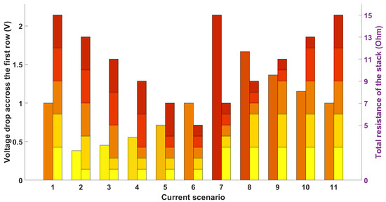
Figure 2.
Single core voltage and stack resistivity of corner cases for a five-stack design. The voltage of the first chip in the stack is shown on the left and the stack resistivity (cumulative and per row) is shown on the right for each of the 11 scenarios.
Scenario 1 of the example in Figure 2 puts every chip in the stack in an idle state. In this case, there is no dynamic current and only leakage applies. This creates an stack of processors. Then, the first chip at the bottom is modeled as if it were operating at maximum computing capacity (scenario 2), then the second chip (scenario 3), and so on until all processors in the stack are turned on and operating at maximum capacity and minimum resistance (scenario 6). Next, the dual of the above condition is applied, starting with all chips turned on. When all chips are operating at maximum capacity, the resistance of the stack is at its lowest value, representing an stack of processors in scenario 6. The chips are then turned off in order starting at the bottom of the stack.
Scenarios 1 and 11 in Figure 2 have maximum stack effective resistance, and scenario 6 has minimum stack resistance. These three scenarios produce the same voltage across the first layer, even though the stack resistance has the maximum variation, because the effective resistance in each layer is the same. Two worst-case voltage corners for the first layer are observed. Scenario 2 provides the lowest voltage to the processor when the equivalent resistance of the first row processor is and the rest are . This layer now receives only 38% of the average voltage per layer. The dual corner appears in scenario 7 when the resistance of the first layer is and the rest are . The voltage supplied to the layer becomes 214% of the average.
Three significant conclusions are derived from this prestudy.
- 1.
- There is a single worst-case value for the largest and smallest voltage supplied to any layer in the stack. All other cases are encompassed between them. Thus, only two scenarios are developed for the models in this paper to show worst-case voltage variation (max and min) for any chip in a voltage stack.
- 2.
- The location of the worst-case layer is independent of the location in the stack. Thus, the model developed in this paper is not location dependent.
- 3.
- The ratio between and has a profound impact on the worst-case values. Thus, chip leakage values are a required parameter of the model developed in this paper. ICs with higher leakage greatly reduce the magnitude of the worst-case values by reducing the gap between and since the leakage power takes a greater portion of the overall power. This dictates that a chip designed for a VS implementation must be designed differently (with more low devices) than a chip for a standard parallel power supply. Stacked-voltage designs with high leakage thereby produce the most robust stacked-voltage implementations. The resistive model shows that stacked-voltage designs are more robust for ICs that are heavily voltage scaled or that employ a leaky process technology node or design methodology.
3.2. A First-Order Model
A resistive first-order model is developed to identify IC sensitivity to changes in supply voltage and is presented in Figure 3. A voltage source supplies a stack composed of resistors consisting of m rows (layers) and n columns. Each resistor can be modified to study the effect of a variation on the rest of the stack. The variable resistor in Figure 3 is the outlying processor with a different effective resistance from the rest of the stack. The other resistors in Figure 3a have the same value (either or ). The resistor stack model is simplified in Figure 3b to combine series and parallel resistors together. The simplified array is parameterized for a simulator such as LTspice® using resistor equations to sweep the parameters. LTspice® is not required to evaluate this model but allows for easy parameterization of the resistors for architectural exploration and enables more complex behaviors and models to be more easily integrated. The and resistors can be combined but are kept independent in this model for improved visualization and to allow modeling voltage offset of the corner case to any layer in the stack.
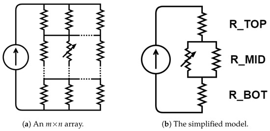
Figure 3.
Models for an array of processing units.
Equations (1)–(3) model the aggregate series resistance above, the parallel resistance at, and series resistance below the outlying processor layer. The variable m is the number of rows, n the number of columns, i the row number of the varying resistor ranging from 2 to , the supply voltage, and P the power dissipated by one chip represented as a resistor. For designs where , it is assumed that only one of the parallel processors in the layer is an outlier and that the rest are in the same mode as the rest of the stack. Chips are usually described through their power consumption at different voltage points rather than their resistivity, thus making these equations apply directly to a specific chip architecture.
When there is one column, the LTspice® model provides a warning that (2) is driven to infinity becoming an open. This creates no discontinuity in the system due to the varying parallel resistor. To model the worst-case position i in the stack at either layer 1 or m, or , respectively, result in a value of 0, which is translated in the simulator by being effectively replaced by a wire.
LTspice® uses to dynamically change the value of a resistor. This approach is used to generate the value of the varying resistor. It is switched between (leakage only) and (maximum computing capacity). represents the initial state and the state after switching. The following equations show how they are used:
The ratio is the metric designers would know from the analysis of the leakage and dynamic current of their chip, and the reason why the system is described in this manner. The ratio is used to generate the new resistance (Equation (5)) and can be described as either a fraction on R or a fraction on I (Equation (4)). The ratio represents the variation in resistance in the system between and . When the ratio is less than one (Equation (6)), and . The resistance decreases and results in an increase in current. This models the change between the idle state and the full-on state. When the ratio is greater than one (Equation (7)), and . The opposite effect is reached and the current decreases, resulting in going from the full-on state to idle state. The value of the ratio is determined by and .
3.3. Limitations and Second-Order Model
This first-order model is developed to assist a designer in optimizing the IC design and system architecture of a stacked-voltage system based on the parameters of stack width and height, dynamic current through a single IC, the leakage current of a chip, and supply voltage ranges. It also provides worst-case corners for a particular design, upon which a mitigation architecture must be based. It is not intended to accurately model a specific architecture with its transients or the absolute voltage the architecture stabilizes at in the presence of negative feedback. The dynamic load produced from processing actual data streams and the random nature of process variation implies that a second-order model would need to be statistical in nature. Such precision may provide more insight into stable operating modes but not worst-case conditions, which are required to plan mitigation strategies for a stacked-voltage design.
When a layer performs more computation than the other layers, its power usage goes up and the equivalent resistance of that layer goes down, leading to a negative feedback loop that makes the voltage of that layer rise. On the flip-side, when less computations are performed, chip power consumption goes down, leading to higher equivalent resistance. This results in a higher voltage to that layer, which produces faster computation and increases dynamic and leakage power. The lower voltage bound is chosen by the chip designers and will typically be above the sub-threshold, where performance decreases exponentially. The upper voltage bound will usually be dictated by the tolerance of the transistors and the ability of the system to remove heat from the ICs and keep the junction temperatures within the desired thermal envelope (e.g., 90 °C). This is especially true for 3D-ICs, which cannot use external heat sinks as efficiently.
This work assumes that parameters are provided for this model by chip designers and system architects such as leakage, min and max chip voltage, source power supply voltage, target performance, number of processors per chip, die size, maximum power and performance of the system, etc. These values are then used to derive and bound the resistances and supply voltages used in this model. Thus, this model allows designers to develop and optimize a chip and voltage-stacked system whilst knowing the effort required for additional control systems and balancing to meet the desired system specifications.
4. Results
4.1. Fundamental Limitations
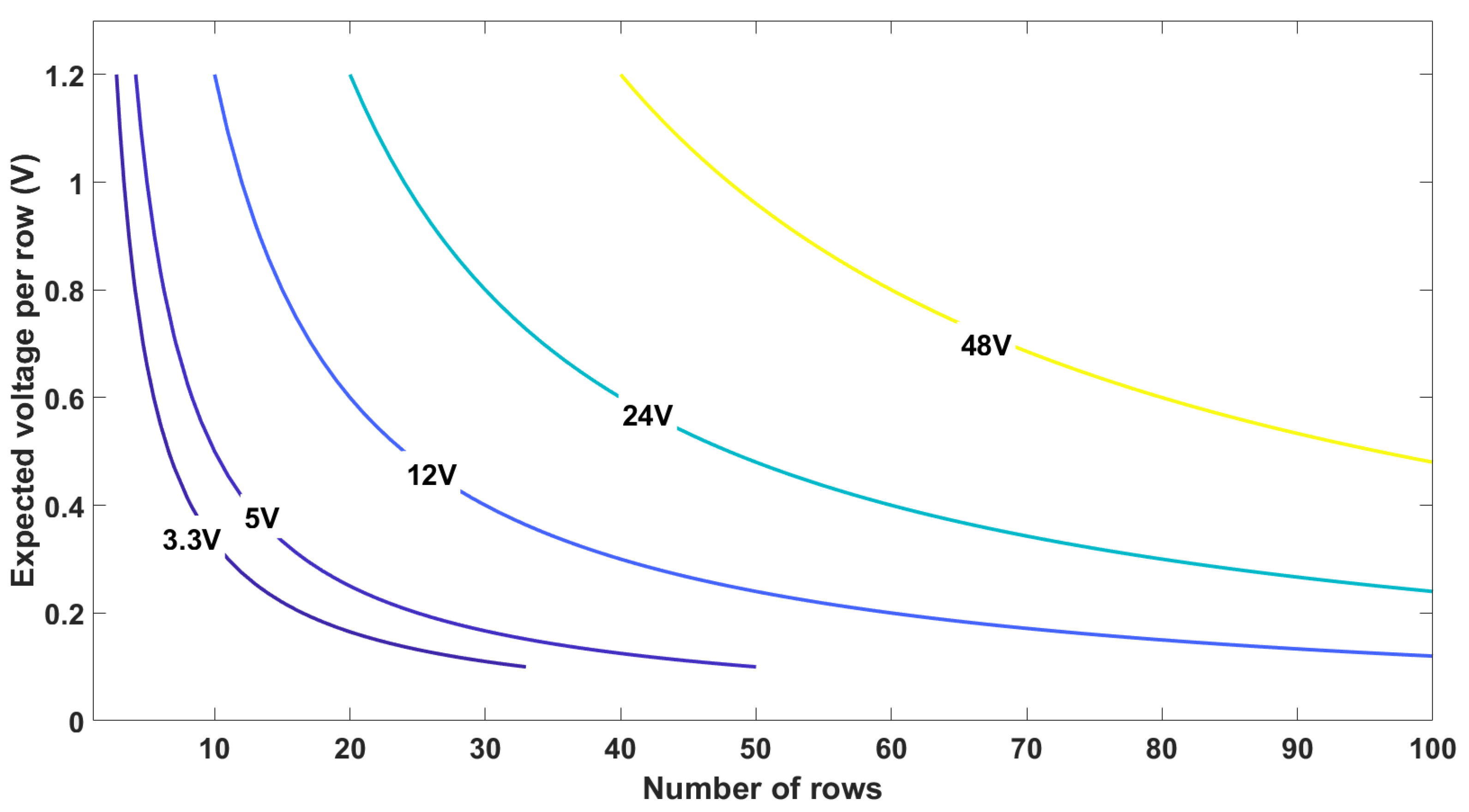
Stacked power systems have fundamental limitations that bound their operation. These include the target voltage supplied to each chip and the thermal limitations of the system or board space. The relationship between nominal chip supply voltage, number of rows in the stack, and system voltage supply is shown in Figure 4. This relationship is represented by Equation (8), where is the system DC voltage supplied to the stack, m is the number of rows or layers, and is the nominal voltage per layer.
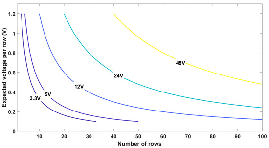
Figure 4.
Interpolated contour of supply voltages ranging from 3.3 V to 48 V achieved with up to 100 rows (x-axis) with nominal voltages per row ranging from 100 mV to 1.2 V (y-axis).
The graph shows chip voltage ranging from 100 mV to 1.2 V per layer and plots five standard supply voltages ranging from 3.3 V to 48 V, where 3.3 V is a typical micro-controller and 48 V is the low-voltage distribution system defined by the US National Electrical Code. As can be seen, the voltage per layer is inversely proportional to the stack height. This limits supply voltage to smaller values for typical IC voltages except for very large row counts.
Since asynchronous processors operate dynamically across a range of voltages, a variable supply voltage can be provided to dynamically adjust the performance and energy efficiency of a stacked-voltage system using DVS (Section 2). A ±5% 5 V supply driving 12 layers will change the average voltage per layer between 438 mV and 396 mV. A ±5% 24 V supply with 58 layers will vary average voltage per layer between 434 mV and 393 mV per layer, which is nearly an identical voltage range per layer. Assuming energy efficiency and performance scale linearly in this voltage range, both of these architectures dynamically operate either at approximately 10% higher performance or 10% lower energy per computation based on the voltage supplied to the system. This shows that studying smaller architectures provides insight into larger ones so long as the behavior of the stack is similar. This can be advantageous for data centers with varying workloads and/or energy costs.
As shown in Section 3.1, the worst-case corner conditions are independent of the overall power consumed by a stacked voltage system. The voltage at each layer is balanced independently of the power consumed in each row. Thus, a separate metric is created to determine the maximum power that can be consumed per chip, per layer, and per power supply. The max rating of the power supply is shown in Equation (9), where p is the average maximum watts per row and m is the number of rows.
This can be used to determine the power per row and power per chip that is required to build such a system. For example, a 3600 W power supply where 100 W are consumed per row admits up to 36 rows. If each chip consumes 25 W, then a 36 × 4 architecture is feasible. This equation allows designers to evaluate trade-offs between system architecture, chip thermals, and die size.
Figure 5 shows the relationship between the number of chips (columns) in a row and the power consumption per row. This relationship is represented by Equation (10), where p is the nominal max power per row, n is the number of columns, and c is the power per chip.
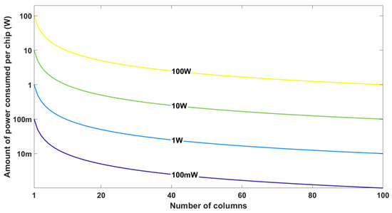
Figure 5.
Power consumption per chip as a function of the maximum watts per row (100 mW–100 W) and the number of columns.
This equation is used to evaluate trade-offs between number of rows, die size, heat removal, board space, and number of columns of the voltage-stacked system. VS system robustness strongly favors more die (columns), but this comes at a cost of board space. Upper bounds will be provided based on thermals, board space, and/or die size. An upper bound on die power consumption—and thus, die size—may be identified based on the thermal density, ability to remove heat, and the desired system cost. For example, using an upper bound of 50 W per row, architectures with one 50 W chip, five 10 W chips, or twenty-five 2 W chips per row are feasible.
Note that each core in a multi-core chip can perform as an independent column in the architecture if each core can be individually controlled. This enables a single chip to behave similarly to a multi-chip architecture. Thus, for example, assume a die with 50 independently controlled engines. A system with a 3600 W power supply and 72 rows can be implemented with 72 chips in a 72 × 1 configuration that is architecturally equivalent to a 72 × 50 architecture, where each chip has a single engine. The board, chip packaging, and heat removal cost of these two hypothetical systems greatly differ.
4.2. Voltage Variation
Voltage variation between layers is possibly the biggest challenge when designing a voltage-stacked system. As shown in Section 3.1, the voltage drop across different layers is the same if and only if the power used by each layer is the same. The worst case occurs when one layer in the stack significantly differs from the rest.
The worst-case scenarios are evaluated by sweeping the equations in Section 3.2, varying the parameters of the number of rows, columns, supply voltage, , and . Five ratios are used above 1 (4, 10, 50, 100, 1000) for when the device goes from fully on to idle, and their inverse (0.25, 0.1, 0.02, 0.01, 0.001) for the opposite transition, resulting in 10 different surfaces. The results are plotted in Figure 6 using a logarithmic scale. The worst case above one is obtained for and the worst case below one with . The model presented in Figure 3b is used for all the results herein and defines how only one resistor differs from the rest. Since all the other cases are contained within those two cases, this implies that reducing the difference between and (more leaky designs) as well as increasing the number of columns in the architecture are the best methods of controlling variation. As can be observed, the number of rows in an architecture has little impact on variation for architectures where the variation is reasonably bound. Thus, the stack height is primarily a parameter of the fundamental limits discussed in Section 4.1.
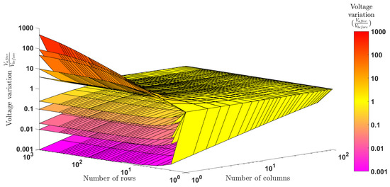
Figure 6.
Voltage variation as ranging from 1 to 1000 columns and rows with different ratios in order from bottom to top [0.001, 0.01, 0.02, 0.1, 0.25, 4, 10, 50, 100, 1000].
Note that the different voltage variations obtained through all the chosen ratios are plotted as instead of using to allow the data to be plotted on a logarithmic scale. Transitions moving from an idle to active state are now plotted as numbers smaller than one rather than negative values.
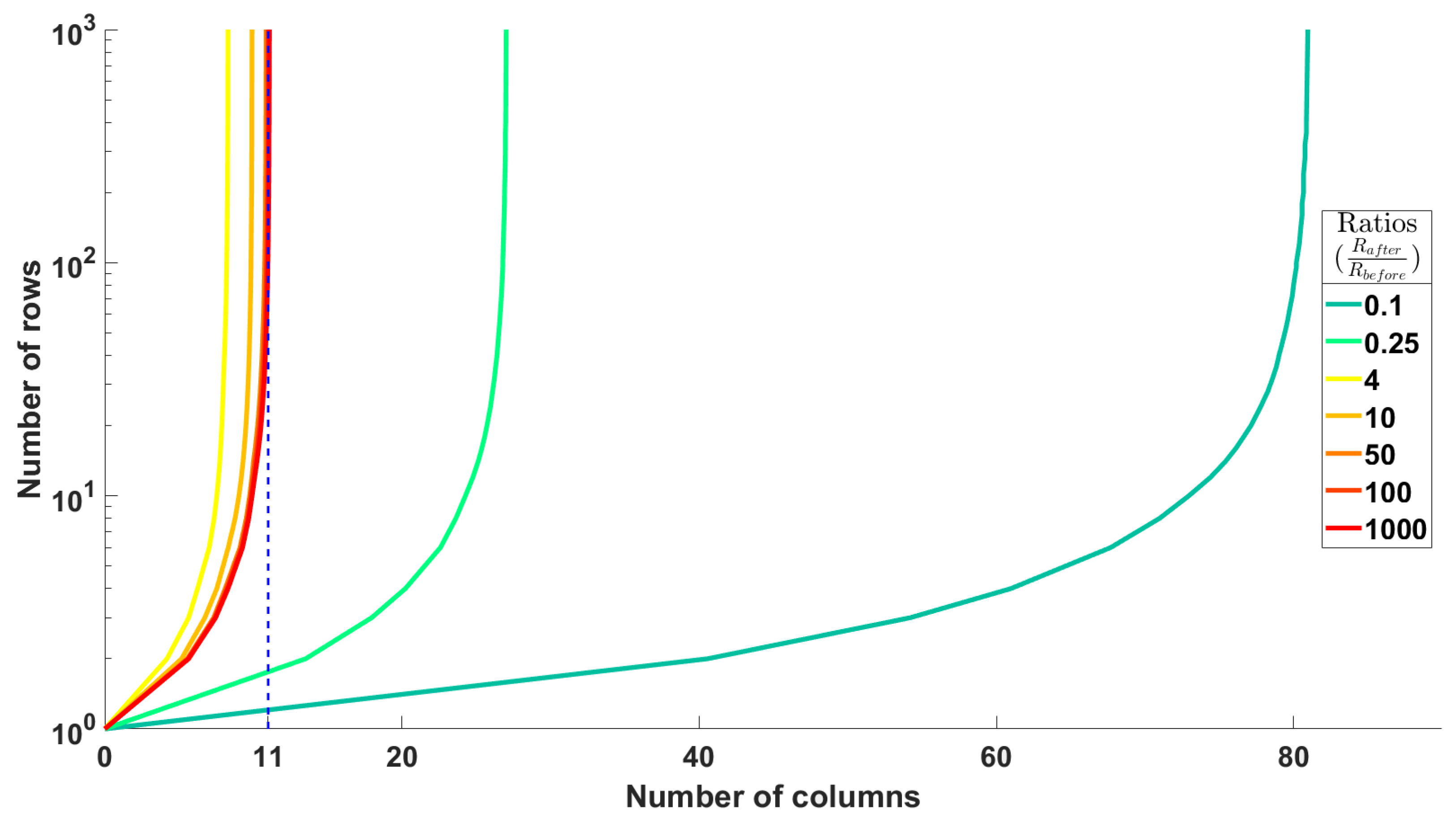
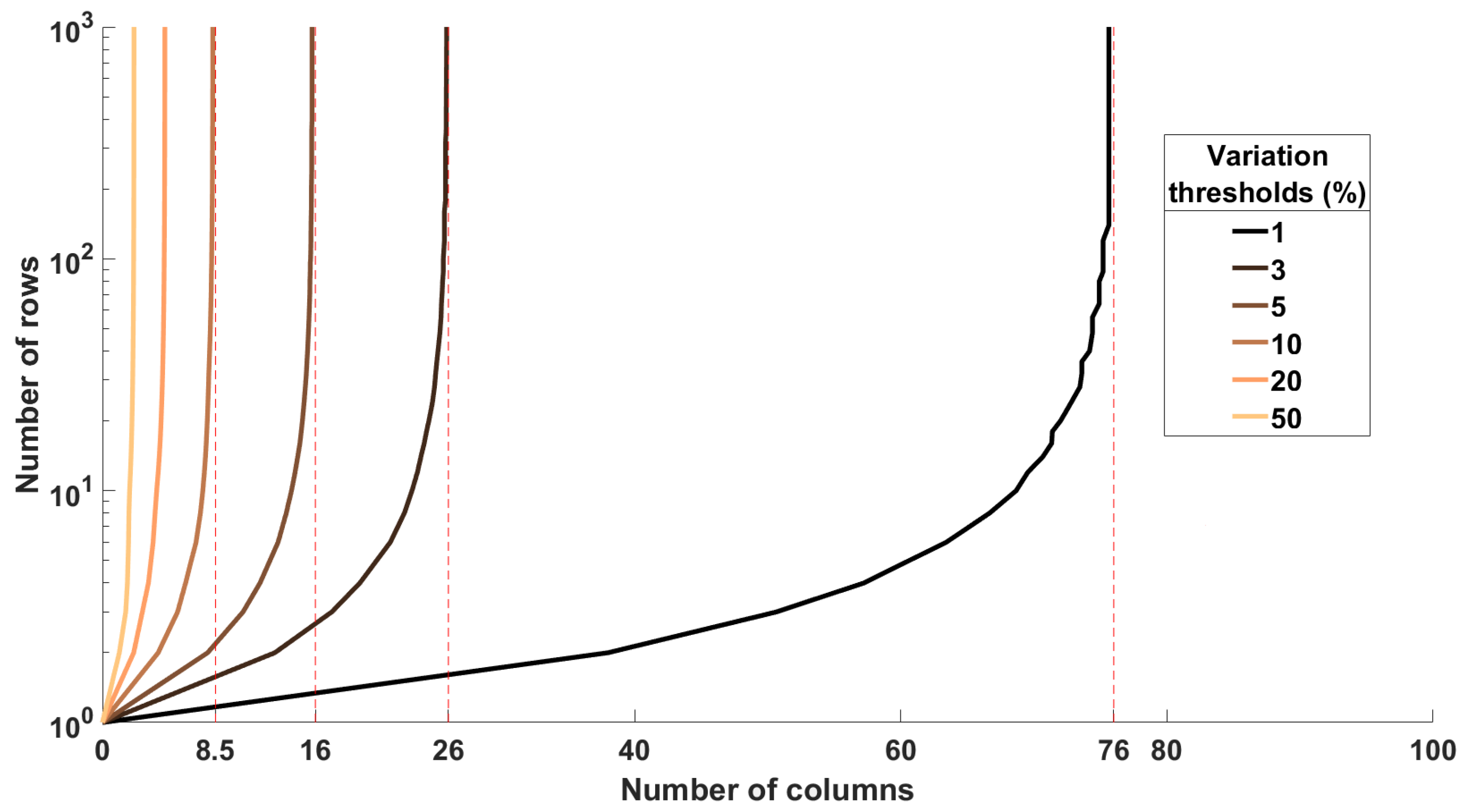
To illustrate this in more detail, two hypothetical cases are extracted from Figure 6 by projecting the data, one in which the variation is limited to 10% but sweeps through the different leakage to active energy ratios (Figure 7) and the other in which the ratio is locked to four but different voltage variation thresholds are evaluated (Figure 8).

Figure 7.
Number of columns required to stay under a 10% variation threshold for different leakage to computation power ratios (0.001 and 0.01 never reach that threshold). Ratio below one is idle to fully on and above one is fully on to idle.
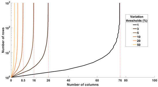
Figure 8.
Number of columns required to stay under different variation thresholds ranging from 1% to 50% for chips with an active to leakage ratio of 0.25 with one going from fully on to idle.
Figure 7 shows the number of columns required to be below a 10% variation threshold. To derive the curves, the intersection between the surfaces defined by the ratio in Figure 6 and a plane defined by a 10% variation are taken, where for the variations above 1 and for those under 1. The yellow to red curves are from the ratios above one when one chip is idle while the rest are at max capacity. The green curves are the ratios below one when one chip is at max capacity while the rest are idle. This clearly shows that robust voltage stacks can be built when one processor is idle and the rest are at max capacity. An asymptotic behavior is reached at 11 columns. Such architectures require no mitigation to keep variation under 10%. The situation is more problematic when one processor is at max capacity and the rest are idle. High-leakage ICs require more than 20 columns in order to avoid external mitigation methods. Lower-leakage chips require 80 or more columns to bound variation between layers at 10%. The closer the ratio is to 1, the fewer the number of columns are required in order to reach the desired voltage variation threshold. This means that the more leakage present in an IC, the easier it becomes to control the variation in voltage. Thus, ICs developed with low-threshold devices where the supply voltage is near threshold are the best application for stacked-voltage configurations that avoid costly mitigation methods.
The reason for the difference in behavior between turning chips on and off is the difference between blocking and pulling current. While blocking current, the current is redirected towards the other columns and the load is shifted. The difference between working on ten columns and nine is 10%, and as this number increases, the difference becomes almost negligible. On the other hand, sinking current is a huge problem. If one column sinks 10 times more current than its counterparts, it will require 10 more columns just to sink the same amount and 100 more to reach the 10% threshold. In terms of application, this means that shutting down a chip is not as problematic as turning one on. The startup condition on the stack must be software supported by slowly and evenly ramping up processors in order to avoid any voltage breakdown. This observation from the linear models can be somewhat tempered by considering the RC effect of negative feedback that exists in a physical IC stack. In either case, adding other systems in parallel—as long as their power usage is far inferior to the rest of the row in idle mode—leads to virtually no voltage variation and potential heterogeneous implementations.
Figure 8 shows the number of columns required to stay under different variation thresholds ranging from 1% to 50% for a given active to leakage power ratio. In this example, 25% of the active power is consumed as leakage, producing a ratio of four. This ratio is controlled through transistor type, supply voltage, and junction temperature. Those curves are the intersection of the surface representing a ratio of four in Figure 6 and the planes z = [1.01, 1.03, 1.05, 1.1, 1.2, 1.5]. This graph shows the benefit of optimizing the architecture of the stacked array as opposed to focusing on costly mitigation approaches to control variation. It becomes increasingly harder as the variation becomes tighter to obtain better results, and the number of columns required increases nonlinearly. With this configuration, 10% variation is achieved with only nine columns and 5% with sixteen. If a design requires a tighter requirement on the voltage variation, hardware compensation and software support will be required.
5. VS Design Example with Mitigation Strategies
An example is presented illustrating the application of the models of this paper in developing a high-current, high-voltage VS implementation. Mitigation strategies are also presented for run time and startup.
The first design constraint in this example is requiring a large supply voltage, which increases the number of rows. Adding more rows increases current recycling, which improves computation efficiency and supply noise. Increasing the number of columns to bring stability to the stack is now limited by the supply wattage. Calculating the worst-case variation with different numbers of columns dictates the supply used and criticality of mitigation approaches. For the IC design, increasing leakage and performance with low- devices provides better stability. If the variation of the VS architecture is above the specified threshold, the number of rows can be reduced and the number of columns increased. This results in a different power supply voltage for the same wattage while keeping the chip supply the same.
For this example, a thermal envelope of 40 W per chip is targeted at a supply voltage of 0.8 V, resulting in 50 A per chip. Two chip designs can be implemented: one with standard-threshold devices (SVT) and another with low-threshold devices (LVT) with higher performance and leakage. Assume the SVT design has an active to leakage ratio of 20, whereas the LVT chip design has a ratio of four.
The current implementation of this product places as many chips as possible in parallel to maximize calculations per second using as many 1kW supplies as needed. This means, in this model, that the limiting factor in terms of the number of rows would be the supply voltage being used when referring to Figure 4 and the number of columns for 1 kW of the supply when referring to Figure 5. For the supply voltage, six rows are supported for a 5 V supply or fifteen rows for a 12 V supply, with any configuration possible in between. The architecture can contain as many as 25 columns, assuming nominal behavior. Thus, a 15 × 20 architecture can be produced using a 12 V, 1 kW power supply.
This architecture can now be evaluated for worst-case power supply variation between rows. Figure 7 shows that such a solution would generate less than 10% variation on the on-to-idle transitions but would be above a 10% threshold on the idle-to-on transitions for both LVT and SVT chip implementations. Figure 8 indicates that for the LVT design, the on-to-idle variation will be between 3 and 5%. This demonstrates that for this design, using LVT devices improves the stability of the stack as well as produces higher performance. Using iso-performance between the two technologies, the total energy consumption can be calculated and one can evaluate whether the LVT-based design is an overall better VS architecture. If the energy consumption is higher with LVT, lowering the supply voltage will permit more rows in the architecture as compensation.
The idle-to-on scenario requires mitigation strategies for both chip designs. The first mitigation strategy is to monitor the states of the chips and to never keep a chip fully on if other chips in the architecture are fully off. Secondly, balancing the computation load across rows is the primary strategy over placing maximal load on a single chip or row. The RC mitigation plan is to share load with other processors in a column. For instance, for a 4 × 4 structure fully on and a desire to turn off four processors, there is a choice of balancing load across rows or columns. Turning off an entire row is the worst-case scenario, whereas turning off one column keeps the voltage in the architecture balanced. The third mitigation strategy requires hardware intervention by implementing some sort of voltage regulator in the stack. The regulator helps stabilize the layer and injects or pulls current if required. Examples of implementations using regulators have been mentioned in the state of the art [8,22,23]. The next mitigation strategy is for transient imbalance only. Sometimes, the load will be different between layers but for a short amount of time. For this, capacitors can be added onboard and create inertia that can be used to generate more power for a short amount of time [24].
Since the worst-case scenario occurs when one layer is on and all the others are off, startup from idle requires significant focus. In the case of a multiple column architecture, columns should be started one at a time so that the rows share the same amount of power needed. In the case of a one-column design, special precautions must be taken in the communication to ensure that data arrive at each layer at the same time. If not, the last row would still be idle while all the others work, generating the worst-case voltage drop.
6. Conclusions
A first-order array model to simulate ICs in a voltage-stacked configuration has been created. Trade-offs in terms of power, voltage, and variation in the supply lines are calculated. This model helps designers optimize voltage-stacked systems and chips that dictate the need to implement mitigation devices and control.
Significant results from this model show that the amount of power drawn from each chip has no direct effect on variation in the stack but rather depends on the difference in power drawn between chips. Variation only depends on the difference in power drawn between fully-on and fully-off chips, regardless of functionality, whether the overall stack consumes a high or low amount of power for a given architecture.
Variation in the supply itself produces a nearly constant variation in voltage in the stack, regardless of the stack height. The location of the variation is shown to be irrelevant. Thermal and supply voltage bounds are presented and their impact on stacked voltage architectures is modeled. Various hypothetical architectures are presented, including configurations of up to 100 rows and 48 V, where variation is less than 10% as long as at least 11 columns are used, possibly eliminating the need for external balancing schemes. Since voltage is balanced independently from the total power consumed, power supply considerations are identified that dictate initial architecture structures, be it for rows, columns, or the supply value. Equations have been presented to derive those values.
The ratio between IC leakage and dynamic power is shown to be a primary metric for creating robust voltage stacks. Thus, optimal designs occur when voltage scaling is applied to produce near threshold operation and/or using technology nodes or thresholds with higher leakage, as this increases the leakage to dynamic power ratio. Adding parallel chips to each row of the stack also significantly reduces variation. A system operating at full capacity, where chips complete computation and one becomes idle, is much more easily controlled by the stacked-voltage architecture without mitigation. An example architecture is shown, where the number of columns required to stay within 5% variation without any compensation system while going from all chips but one in the stack being fully operating is just 11 columns when leakage is 25% of the active power. The model clearly identifies the condition of ramping up computation as the largest problem in a voltage-stacked system. This process is shown to almost certainly require software control and/or hardware mitigation to ensure a balanced transition from idle to busy states. Finally, heterogeneous applications can be used without additional mitigation when the power used by one chip is insignificant compared to the overall power of the row.
The results obtained from these first-order models present new and significant understanding and bounds to the design and optimization of voltage-stacked systems. These data enable chip designers and system architects to rapidly evaluate and construct robust voltage-stacked systems that minimize the requirement for mitigation methods to control voltage variation between layers in the stack. It also allows for better communication between chip and PCB designers early on in the process regarding chip characteristics; on board components needed—since VS replaces traditional voltage conversion, might add voltage balancing components, and could potentially require a large amount of space for larger architectures; and off board components.
Author Contributions
Conceptualization, B.C. and K.S.S.; methodology, B.C.; software, B.C.; validation, B.C. and K.S.S.; formal analysis, B.C.; investigation, B.C.; resources, K.S.S.; data curation, B.C.; writing—original draft preparation, B.C.; writing—review and editing, K.S.S.; visualization, B.C.; supervision, K.S.S.; project administration, K.S.S.; funding acquisition, K.S.S. All authors have read and agreed to the published version of the manuscript.
Funding
This research received no external funding.
Data Availability Statement
No data are available online. The data that support the findings of this study can be available from the corresponding author upon reasonable request.
Conflicts of Interest
The authors declare no conflict of interest.
References
- Zhai, B.; Blaauw, D.; Sylvester, D.; Flautner, K. Theoretical and Practical Limits of Dynamic Voltage Scaling. In Proceedings of the 41st Annual Design Automation Conference, San Diego, CA, USA, 7–11 June 2004; pp. 868–873. [Google Scholar]
- Rajapandian, S.; Xu, Z.; Shepard, K. Energy-Efficient Low-Voltage Operation of Digital CMOS Circuits Through Charge-Recycling. In Proceedings of the 2004 Symposium on VLSI Circuits. Digest of Technical Papers, Honolulu, HI, USA, 17–19 June 2004; pp. 330–333. [Google Scholar]
- Rajapandian, S.; Shepard, K.; Hazucha, P.; Karnik, T. High-Voltage Power Delivery Through Charge Recycling. IEEE J. Solid-State Circuits 2006, 41, 1400–1410. [Google Scholar] [CrossRef]
- McClurg, J.; Zhang, Y.; Wheeler, J.; Pilawa-Podgurski, R. Re-Thinking Data Center Power Delivery: Regulating Series-Connected Voltage Domains in Software. In Proceedings of the 2013 IEEE Power and Energy Conference at Illinois (PECI), Urbana, IL, USA, 22–23 February 2013; pp. 147–154. [Google Scholar]
- Lee, S.K.; Brooks, D.; Wei, G. Evaluation of Voltage Stacking for Near-Threshold Multicore Computing. In Proceedings of the 2012 ACM/IEEE International Symposium on Low Power Electronics and Design (ISLPED), Redondo Beach, CA, USA, 30 July–1 August 2012; pp. 373–378. [Google Scholar]
- Lee, S.K.; Tong, T.; Zhang, X.; Brooks, D.; Wei, G.Y. A 16-core voltage-stacked system with an integrated switched-capacitor DC-DC converter. In Proceedings of the 2015 Symposium on VLSI Circuits (VLSI), Kyoto, Japan, 17–19 June 2015; pp. C318–C319. [Google Scholar]
- Xu, K.; Zhuldassov, N.; Friedman, E.G. Tile-Based Power Delivery Networks for High Current, Voltage Stacked Systems. IEEE Trans. Components Packag. Manuf. Technol. 2021, 11, 1097–1105. [Google Scholar] [CrossRef]
- Xu, K.; Friedman, E.G. Challenges in High Current On-Chip Voltage Stacked Systems. In Proceedings of the 2020 IEEE International Symposium on Circuits and Systems (ISCAS), Seville, Spain, 12–14 October 2020; IEEE: Piscataway, NJ, USA, 2020; pp. 1–5. [Google Scholar]
- Zou, A.; Leng, J.; He, X.; Zu, Y.; Gill, C.D.; Janapa Reddi, V.; Zhang, X. Voltage-Stacked GPUs: A Control Theory Driven Cross-Layer Solution for Practical Voltage Stacking in GPUs. In Proceedings of the 2018 51st Annual IEEE/ACM International Symposium on Microarchitecture (MICRO), Fukuoka, Japan, 20–24 October 2018; pp. 390–402. [Google Scholar]
- Zou, A.; Leng, J.; He, X.; Zu, Y.; Gill, C.D.; Reddi, V.J.; Zhang, X. Voltage-Stacked Power Delivery Systems: Reliability, Efficiency, and Power Management. IEEE Trans. Comput.-Aided Des. Integr. Circuits Syst. 2020, 39, 5142–5155. [Google Scholar] [CrossRef]
- Cabe, A.C.; Qi, Z.; Stan, M.R. Stacking SRAM Banks for Ultra Low Power Standby Mode Operation. In Proceedings of the Design Automation Conference (DAC), Anaheim, CA, USA, 13–18 June 2010; pp. 699–704. [Google Scholar]
- Li, X.; Xu, Y.; Ren, L.; Ge, W.; Cai, J.; Liu, X.; Yang, J. 29.8 115nA@3V ULPMark-CP Score 1205 SCVR-Less Dynamic Voltage-Stacking Scheme for IoT MCU. In Proceedings of the 2021 IEEE International Solid-State Circuits Conference (ISSCC), San Francisco, CA, USA, 13–22 February 2021; Volume 64, pp. 100–102. [Google Scholar]
- Liu, X.; Li, X.; Zhang, H.; Li, C.; Ren, L.; Chen, Q.; Xu, Y.; Yang, J. SCVR-Less Dynamic Voltage-Stacking Scheme for IoT MCU. IEEE J. Solid-State Circuits 2022, 57, 103–114. [Google Scholar] [CrossRef]
- Singh, K.; de Bruin, B.; Jiao, H.; Huisken, J.; Corporaal, H.; de Gyvez, J.P. Converter-Free Power Delivery Using Voltage Stacking for Near/Subthreshold Operation. IEEE Trans. Very Large Scale Integr. (VLSI) Syst. 2021, 29, 1039–1051. [Google Scholar] [CrossRef]
- Zhang, R.; Mazumdar, K.; Meyer, B.H.; Wang, K.; Skadron, K.; Stan, M.R. Transient Voltage Noise in Charge-Recycled Power Delivery Networks for Many-Layer 3D-IC. In Proceedings of the 2015 IEEE/ACM International Symposium on Low Power Electronics and Design (ISLPED), Rome, Italy, 22–24 July 2015; pp. 152–158. [Google Scholar]
- Zhang, R.; Mazumdar, K.; Meyer, B.H.; Wang, K.; Skadron, K.; Stan, M. A Cross-Layer Design Exploration of Charge-Recycled Power-Delivery in Many-Layer 3D-IC. In Proceedings of the 2015 52nd ACM/EDAC/IEEE Design Automation Conference (DAC), San Francisco, CA, USA, 8–12 June 2015; pp. 1–6. [Google Scholar]
- Jain, P.; Kim, T.H.; Keane, J.; Kim, C.H. A Multi-Story Power Delivery Technique for 3D Integrated Circuits. In Proceedings of the 13th International Symposium on Low Power Electronics and Design (ISLPED ’08), Bangalore, India, 11–13 August 2008; pp. 57–62. [Google Scholar]
- Wang, Z.; Zheng, L.; Lin, Z.; Zhao, J.; Tang, W.; Feng, L.; Liu, Z.; Li, X.; Guo, X.; Si, M. CMOS Logic and Capacitorless DRAM by Stacked Oxide Semiconductor and Poly-Si Transistors for Monolithic 3-D Integration. IEEE Trans. Electron Devices 2024, 71, 4664–4669. [Google Scholar] [CrossRef]
- Burd, T.D.; Brodersen, R.W. Design Issues for Dynamic Voltage Scaling. In Proceedings of the 2000 International Symposium on Low Power Electronics and Design, Rapallo, Italy, 26–27 July 2000; pp. 9–14. [Google Scholar]
- Thielemans, T.; Butzen, N.; Sarafianos, A.; Steyaert, M.; Tavernier, F. A Capacitive DC-DC Converter for Stacked Loads With Wide Range DVS Achieving 98.2% Peak Efficiency in 40nm CMOS. In Proceedings of the 2018 IEEE Custom Integrated Circuits Conference (CICC), San Diego, CA, USA, 8–11 April 2018; IEEE: Piscataway, NJ, USA, 2018; pp. 1–4. [Google Scholar]
- Tseng, N.H.; Wu, B.K.; Huang, T.P.; Lee, C.Y.; Chen, K.H.; Lin, Y.H.; Lin, S.R.; Tsai, T.Y. A Series Stacked FinFET Structure for Digital Low Dropout Regulators with Minimum Energy Point Technique for 37.5% Energy Reduction in Cortex M0 Processor. In Proceedings of the 2021 IEEE International Symposium on Circuits and Systems (ISCAS), Daegu, Republic of Korea, 22–28 May 2021; IEEE: Piscataway, NJ, USA, 2021; pp. 1–4. [Google Scholar]
- Mace, J.; Noh, G.; Ha, J.I. Modeling and Design of Switched-Capacitor Converters for Voltage Stacking. In Proceedings of the 2020 IEEE 9th International Power Electronics and Motion Control Conference (IPEMC2020-ECCE Asia), Nanjing, China, 29 November–2 December 2020; IEEE: Piscataway, NJ, USA, 2020; pp. 503–510. [Google Scholar]
- Chen, S.; Li, C.; Lu, Z.; Luo, H.; Li, W.; He, X. A Coupled Inductor Based Circuit for Voltage Balancing among Series Connected SiC MOSFETs. In Proceedings of the 2020 IEEE Applied Power Electronics Conference and Exposition (APEC), New Orleans, LA, USA, 15–19 March 2020; IEEE: Piscataway, NJ, USA, 2020; pp. 2588–2593. [Google Scholar]
- Lee, S.K. High Efficiency Power Delivery for Chip Multiprocessors Using Voltage Stacking. Ph.D. Thesis, Harvard University, Graduate School of Arts & Sciences, Cambridge, MA, USA, 2016. [Google Scholar]
Disclaimer/Publisher’s Note: The statements, opinions and data contained in all publications are solely those of the individual author(s) and contributor(s) and not of MDPI and/or the editor(s). MDPI and/or the editor(s) disclaim responsibility for any injury to people or property resulting from any ideas, methods, instructions or products referred to in the content. |
© 2024 by the authors. Licensee MDPI, Basel, Switzerland. This article is an open access article distributed under the terms and conditions of the Creative Commons Attribution (CC BY) license (https://creativecommons.org/licenses/by/4.0/).

