Abstract
A power-efficient 16-bit 1-MS/s successive approximation register (SAR) analog-to-digital converter (ADC) is presented in this paper. High-bit sampling makes the bridge capacitance in the digital-to-analog converter (DAC) a unit one, eliminating fractional capacitance mismatch. The high-precision comparator is composed of a four-stage preamplifier and a strong-arm latch, with auto-zeroing used to mitigate input offset further. Digital foreground calibration based on low-bit weight is implemented to correct DAC capacitance mismatch. The post-layout simulation results show that the core ADC achieves 95.61 dB SNDR and 105.1 dB SFDR with calibration, consuming 5.4 mW power under a 3.3 V supply voltage, corresponding to a Schreier figure of merit (FoM) of 175.3 dB. The ADC core area is 1.06 mm2 in the 180 nm CMOS technology.
1. Introduction
The majority of signals in nature are analog signals, and in order to take full advantage of the computing performance of digital circuits, an analog-to-digital converter (ADC) is essential. ADCs are responsible for converting an analog signal, which is continuous in both time and amplitude, into a discrete digital signal that can be processed by a digital circuit. ADCs are increasingly the performance bottleneck of overall electronic systems. In recent years, successive approximation register (SAR) ADCs become popular due to their low power consumption, small area and simple structure [1,2,3]. High-resolution SAR ADCs with relatively low speed are widely used in applications ranging from instrumentation and medical electronics to mobile wearable devices, etc. [4,5,6,7,8].
However, as the resolution exceeds 10 bits, the accuracy of the SAR ADC is affected by capacitance mismatch, comparator noise and offset, etc. [9,10,11,12]. To mitigate comparator offset, three techniques are employed: trimming, chopping and auto-zeroing. Trimming is used to measure and compensate offset voltage by a specific method after chip manufacturing, but it is not suitable for high-precision designs. Chopping [13] utilizes continuous-time modulation to shift the offset voltage to a higher frequency for filtering. This technique can not only eliminate the offset voltage of the comparator but also mitigate the noise. However, this method requires a higher frequency clock and results in a more complex circuit design. Auto-zeroing [14,15,16] is to store the offset voltage in the form of charge on the capacitance. The role of the capacitance is equivalent to that of a voltage source; its size is approximately equal to the size of the offset voltage, the polarity is opposite to the offset voltage, and then in the normal working stage the offset is eliminated. Auto-zeroing is classified as input offset storage (IOS) and output offset storage (OOS) based on the position of the capacitance in the preamplifier’s input and output.
To mitigate the effect of capacitance mismatch, several calibrations have been explored. A classic self-calibrating technique is proposed in [17]. In the calibration phase, the voltage error caused by capacitance mismatch is firstly measured by an additional calibration digital-to-analog converter (DAC) and stored in a data register, and then used to correct the mismatch error of the capacitive digital-to-analog converter (CDAC) in the conversion phase. However, the implementation of this calibration requires an additional block circuit and a large area. A foreground digital calibration is proposed in [18,19], which considers low-bit capacitances as the ideal ones and uses them to estimate the weight of high-bit capacitances. However, the weight estimation errors of LSB capacitances will propagate exponentially to those of MSB ones. A background digital calibration technique based on dither is proposed in [20], which obtained two sets of digital output codes by stacking the offset of +Δ and −Δ, respectively, in the sampling process and quantizing them twice. For linear systems, the disturbed signal can be eliminated without affecting the quantization of the input signal. However, an SAR ADC with capacitance mismatch is a nonlinear system, and its nonlinear part will have errors after quantization. Through this error value, the weight error of each capacitance can be obtained and the weight of each capacitance can be adjusted by the LMS algorithm until the error is zero. A double-conversion background calibration technique is proposed in [21], applied to a 20-bit 1-MS/s SAR ADC. This technique mainly converts each analog sample twice through a single SAR ADC and modulates the error between the two conversions. It is clear that with the rapid development of the technology, more and more calibration technologies are developing in the direction of digitalization.
This paper presents a 16-bit 1-MS/s SAR ADC. The segmented capacitance array is utilized to reduce the capacitance area and the mismatch caused by fractional capacitance is eliminated via high-bit sampling. To solve insufficient setting of high-bit capacitances, redundant bits are introduced to the capacitance array of the MSB segment. To minimize the comparator’s input offset voltage, a four-stage preamplifier and a latch with the auto-zeroing technique are used. In order to reduce the accuracy degradation of the ADC due to capacitance mismatch, a digital foreground calibration technique based on low-bit weight is designed. The ADC is designed in 180 nm CMOS technology under a 3.3 V supply voltage.
2. Simulation Results
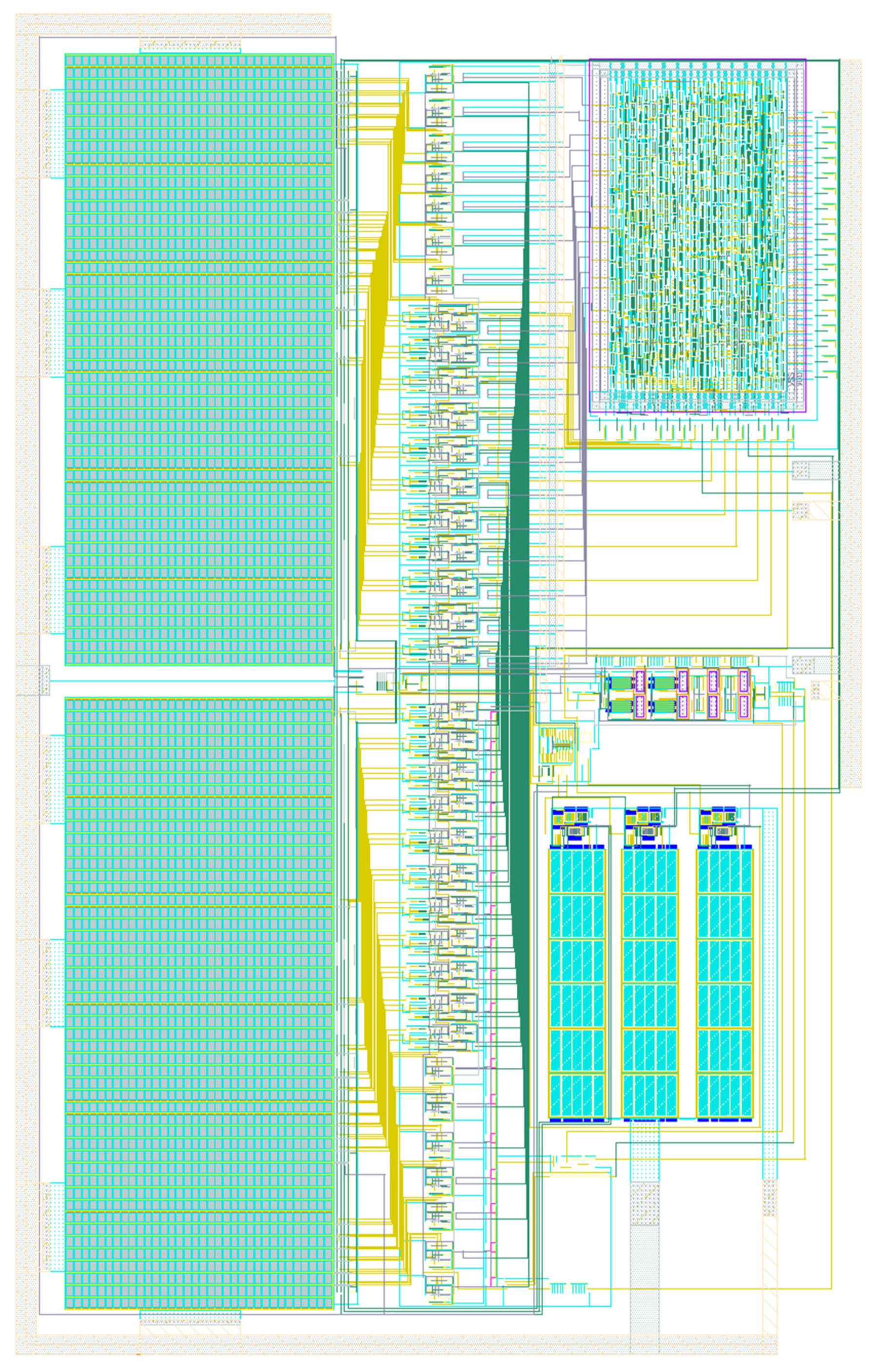
The 16-bit SAR ADC has been designed in a 0.18 um CMOS and its layout is shown in Figure 1; the area of the ADC core is 0.83 mm × 1.28 mm. The layout of the timing part of the digital calibration algorithm is generated using a digital back-end layout routing tool and the active area of the layout of the digital calibration part is 0.21 mm × 0.35 mm. Both the power supply and the reference voltage are 3.3 V. We assume that the circuit noise is smaller than other noise components in this paper. Figure 2 shows the effective number of bits (ENOB) of the ADC under 27 PVT conditions without capacitance mismatch at 476.56 kHz input frequency. The process corners are TT, SS and FF, with temperatures of −40 °C, 40 °C and 85 °C and power supply voltages of 3 V, 3.3 V and 3.6 V, respectively. It can be seen that the ENOB of the ADC under all PVT conditions is greater than 15 bits, and the ADC features good robustness.
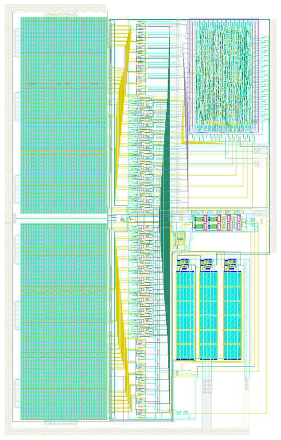
Figure 1.
The layout of the presented SAR ADC.
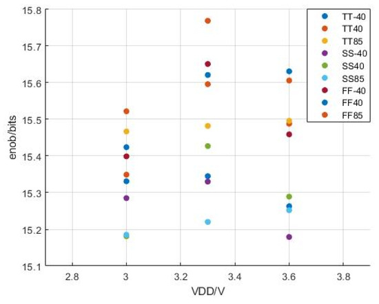
Figure 2.
The ENOB of ADC under 27 PVT conditions without capacitance mismatch.
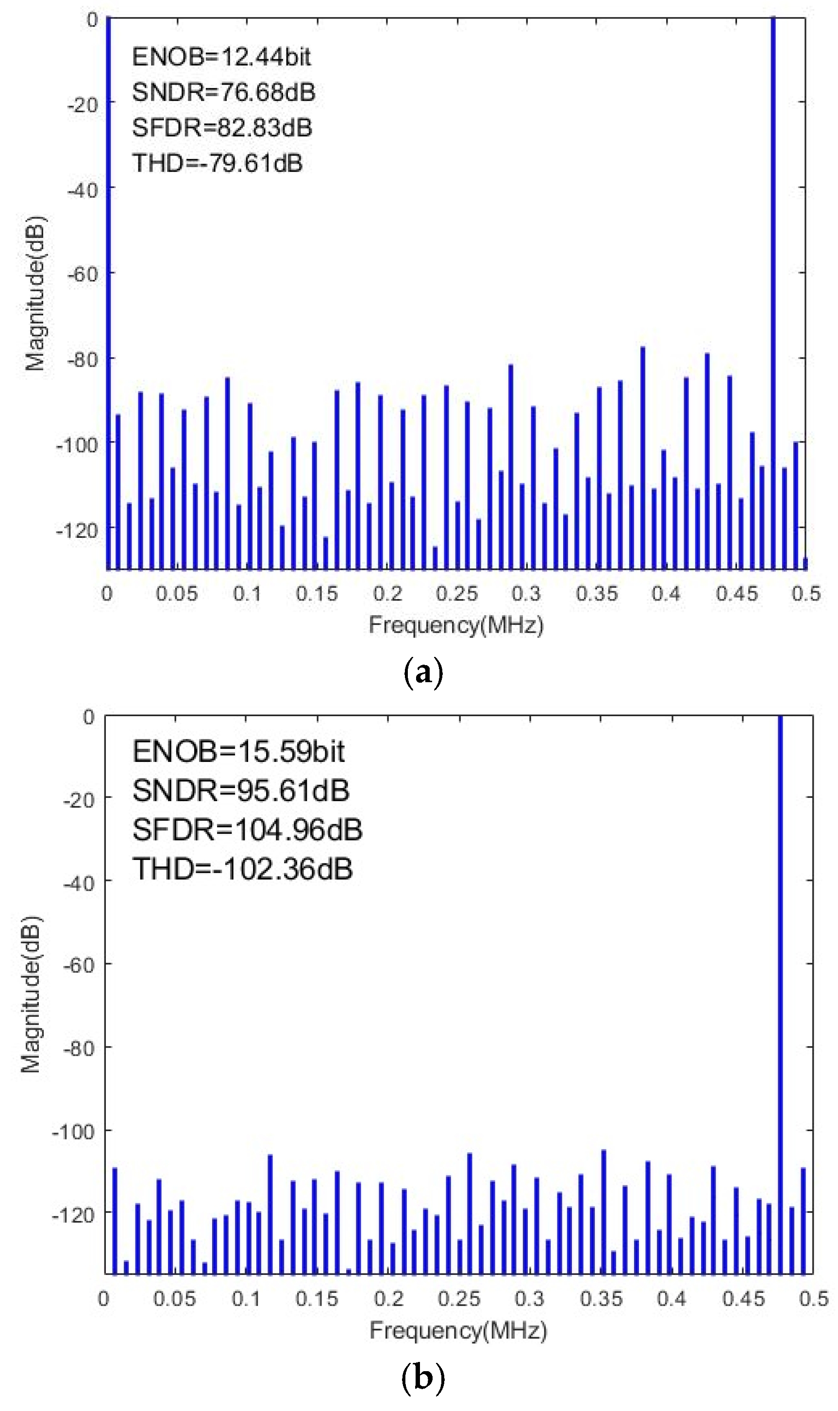
Figure 3 shows the post-simulated power spectrum density (PSD) of the ADC, which is driven by a 1 MS/s clock and a 475.56 kHz full-scale sine input signal. For comparison, simulation results both with and without digital calibration are presented. After calibration, large harmonic distortions are significantly suppressed, and the SAR ADC’s signal-to-noise-distortion ratio (SNDR) and spurious-to-free dynamic range (SFDR) are improved from 76.68 dB and 82.83 dB to 95.61 dB and 104.96 dB, respectively. The core ADC consumes 5.4 mW, corresponding to an FoM of 175.3 dB. Table 1 shows the post-simulation results at different PVT conditions with and without calibration at 475.56 kHz input signal. Under the condition of SS 3.6 V −40 °C, the ADC’s ENOB is the lowest (14.98 bits) after calibration and at other corners the ENOB is all greater than 15 bits after calibration, indicating that the calibration has good stability.
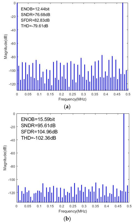
Figure 3.
(a) Post–simulated SAR ADC PSD without digital calibration. (b) Post–simulated SAR ADC PSD with digital calibration.

Table 1.
Post-simulation results under different PVT corners with and without calibration.
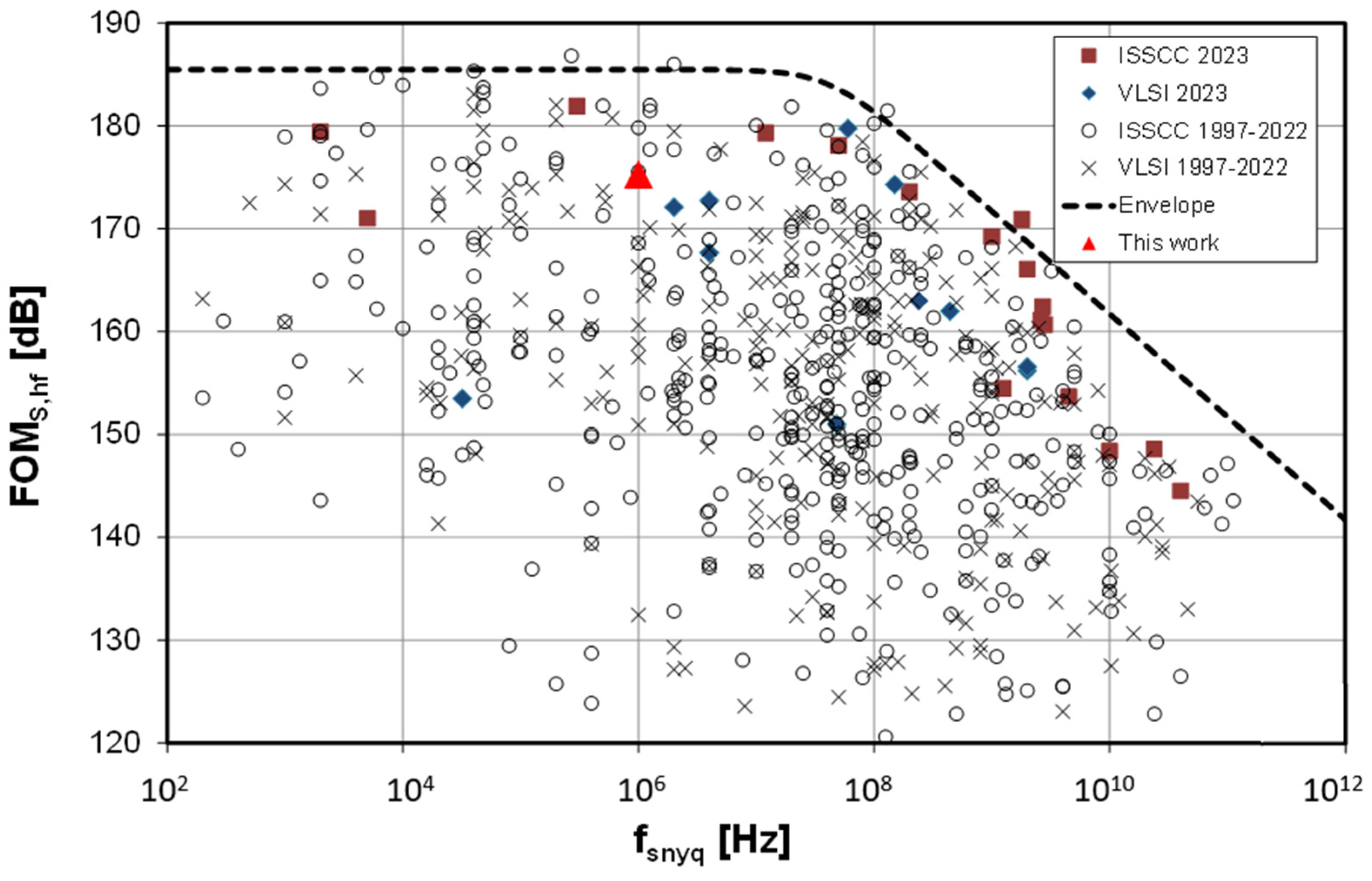
The power consumption breakdown of the SAR ADC is shown in Figure 4. The main power consumption is in the comparator, accounting for 77.7%, followed by the CDAC and sampling circuit, which consume 18.9% in total, and the digital logic circuit consumes 3.4%. The result of this design is added to Boris Murmann’s Schreier FoM vs. speed plot [22] for comparison, as shown in Figure 5. It shows that the designed 16-bit SAR ADC achieves good performance. Table 2 summarizes the performance of the presented SAR ADC and compares it with the state of the art. The results show that the proposed SAR ADC achieves competitive SNDR and SFDR after calibration. The ADC presented in [23] can operate at a higher sampling rate, but the proposed ADC has a higher resolution and consumes less power. Compared to the proposed ADC, the ADC in [4] features a similar resolution and sampling rate but it lacks the calibration circuit, which is implemented in an off-chip FPGA. Due to the use of a pipeline-SAR structure, the sampling rate of the ADCs presented in [24,25] is higher, but the proposed ADC has a higher resolution and SNDR.
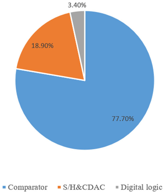
Figure 4.
Power consumption breakdown of the SAR ADC.
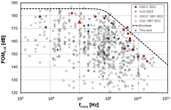
Figure 5.
Boris Murmann’s Schreier FoM vs. speed plot with this design.

Table 2.
Performance summary and comparison to state-of-the-art designs.
3. SAR ADC Architecture and Digital Calibration
3.1. SAR ADC Architecture
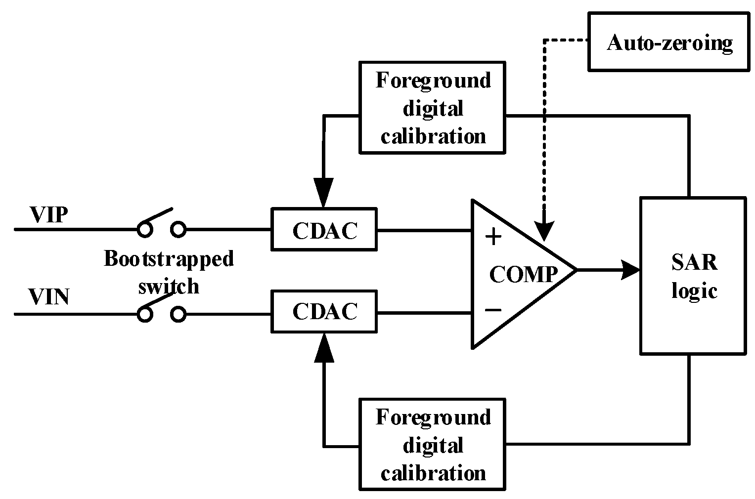
The simplified block diagram of the presented 16-bit 1-MS/s SAR ADC is shown in Figure 6, which consists of a pair of bootstrapped switches, a differential segmented CDAC with digital foreground calibration, a high-precision comparator with auto-zeroing, and SAR logic. Auto-zeroing is used to eliminate the offset voltage of the comparator, and the digital foreground calibration aims to minimize the performance degradation caused by CDAC capacitance mismatch.

Figure 6.
Architecture of the presented 16-bit 1 MS/s SAR ADC.
3.2. DAC Foreground Calibration
If no DAC calibration is applied, a unit capacitance of 600 fF and a total capacitance of 633 pF are required to guarantee 16-bit linearity. Such a large capacitance would result in a large chip area and a high power consumption to drive it. To overcome the design penalty, a differential DAC digital foreground calibration based on [18] is designed in this SAR ADC.
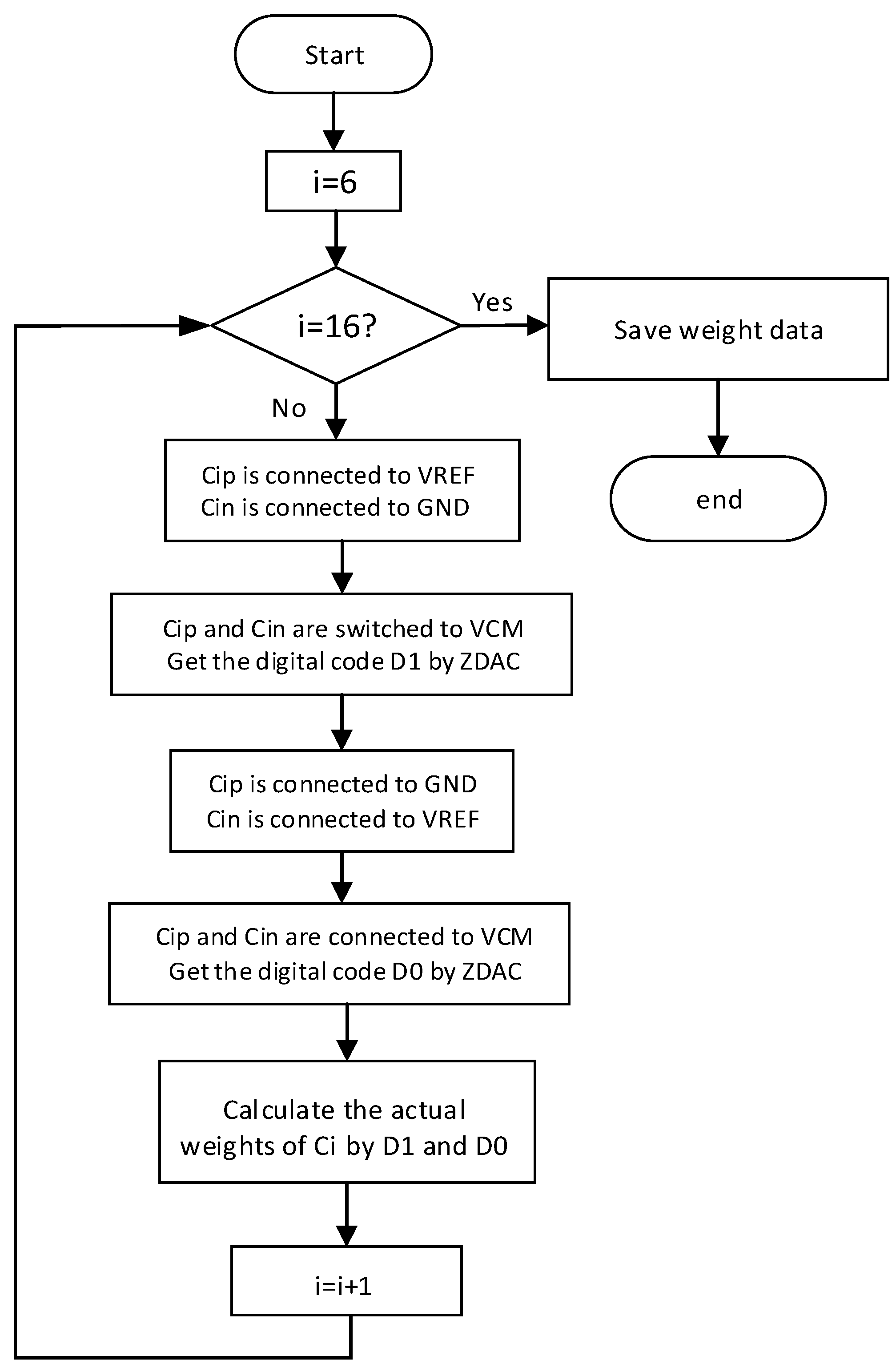
The capacitances in the LSB array are regarded as ideal capacitances and used as the calibration capacitance array ZDAC and to calibrate capacitances C6p and C6n. The calibration procedure is as follows: (1) The bottom plate of C6p is connected to Vref, the bottom of C6n is connected to GND and those of all other capacitances are connected to the common-mode voltage (Vcm). The top plates of all capacitances are connected to Vcm. (2) C6p and C6n are switched to Vcm, and ZDAC is used to generate the digital code D6,1. (3) The bottom plate of C6p is switched to GND, and C6n is switched to Vref; the operation is repeated in the second step and ZDAC is used to obtain the digital code D6,0. The difference between these two codes is the estimated weight of C6p and C6n. The weight values of C6p and C6n are updated. (4) The new ZDAC capacitances are used to calibrate the next capacitances C7p and C7n; the new ZDAC is now composed of C0p~C6p and C0n~C6n, and so on, until the MSB capacitances C16p and C16n are calibrated, as shown in Figure 7. After the updated weight value of the MSB array capacitance is obtained, it is digitally processed with the output code in the normal conversion stage to reduce the influence of capacitance mismatch. In implementation, multiple measurements and averaging can be applied to reduce circuit noise and improve calibration accuracy.

Figure 7.
Foreground calibration procedure of the CDAC.
4. SAR ADC Circuit Implementation
4.1. Bootstrapped Switch
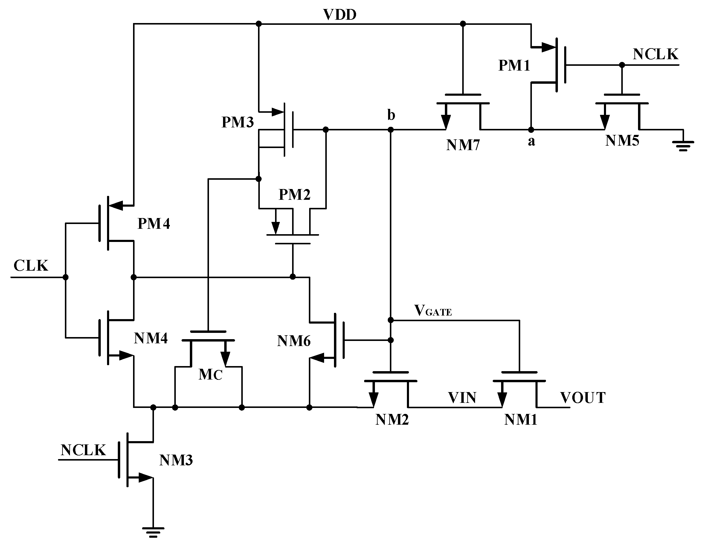
MOS switches introduce nonlinearity because their on-resistance will change with the input signal. In order to minimize the variation in switch on-resistance, the bootstrapped switch as shown in Figure 8 is adopted in this paper. CLK is the sampling clock, NCLK is the reverse signal of the sampling clock and an Mc transistor is used to act as the capacitance. In the holding stage, CLK is low and NCLK is high. Transistors NM5 and NM7 are on. The gate voltage of transistor NM1 is pulled to the ground, so NM1 is off, and the output voltage remains in the original state. The MOS capacitance Mc is charged to VDD. In the sampling stage, CLK is high and NCLK is low. Transistors NM3 and PM3 are off and transistors NM2 and PM2 are on. As a result, the bottom plate of the MOS capacitance is connected to the source of NM1 through NM2, while the top plate of the MOS capacitance is connected to the gate of transistor NM1 through PM2. Due to the conservation of charge, the voltage difference between the top and bottom plates of the MOS capacitance remains VDD. Therefore, the gate-to-source voltage of transistor NM1 remains at VDD, so the gate voltage of the NM1 transistor is Vin + VDD.

Figure 8.
Schematics of the bootstrapped switch.
4.2. Capacitive DAC
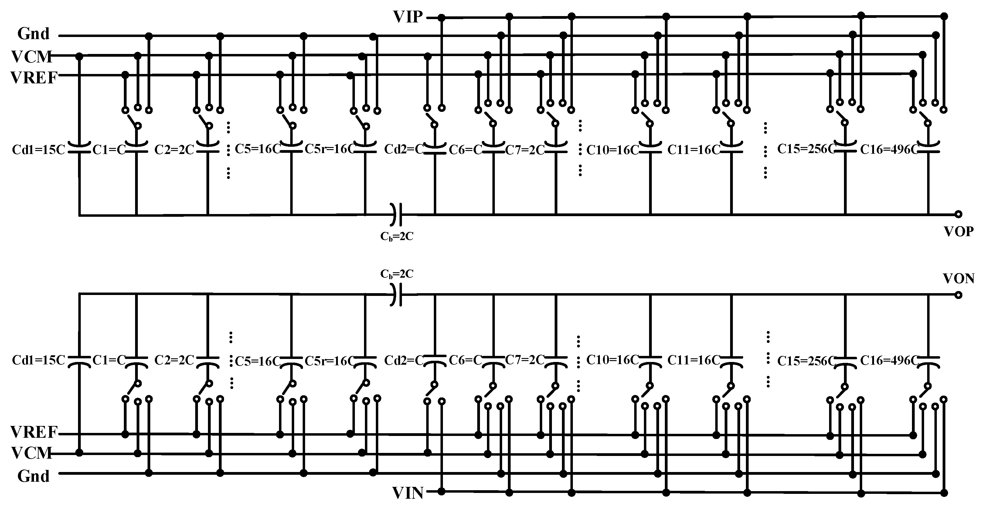
For the traditional CDAC structure, the total capacitance increases exponentially as the number of bits increases. The use of a segmented capacitance array (SCA) with a bridge capacitance is a common solution for high-resolution SAR ADC, but the large number of bits in the LSB array increases with the nonlinearity of the circuit [28]. Based on the above trade-off, the MSB array and LSB array have 10-bit and 6-bit resolutions, respectively. Moreover, the bridge capacitance of traditional segmented CDAC is usually a fractional capacitance, introducing capacitance mismatch and degrading ADC accuracy. In this paper, the two-segment capacitance array is designed and optimized, as shown in Figure 9. Because only capacitances of the high segment are used as sampling capacitances, the bridge capacitance (CB) can be designed as a unit capacitance. To solve the insufficient setting of high-bit capacitances, the binary-scaled recombination redundance algorithm is utilized in the MSB array [29,30]. Meanwhile, one-bit redundancy is assigned to the LSB array for CDAC calibration. Since the introduction of the redundant bit capacitance of the LSB array will cause the weight value of the LSB array relative to the MSB array to change, the bridge capacitance is changed to a value of twice the unit capacitance and the dummy capacitance of Cd1 = 15 Cu is introduced in the LSB array to ensure that the linear requirement of the ADC is met.
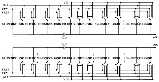
Figure 9.
Schematics of the two-segment CDAC.
The value of the unit capacitance is mainly determined by two factors: sampling thermal noise and capacitance mismatch. The capacitance mismatch calibration technology is adopted in this paper, so the requirement of sampling thermal noise on unit capacitance can be mainly considered.
The kT/C noise power can be expressed as
where k is the Boltzmann constant, T is the thermodynamic temperature and Cs is the total sampling capacitance.
Taking into account comparator noise, the sampling thermal noise of CDAC needs to be less than half of the quantization noise:
To maintain the design margin, the value of unit capacitance is set as 30 fF.
4.3. Comparator
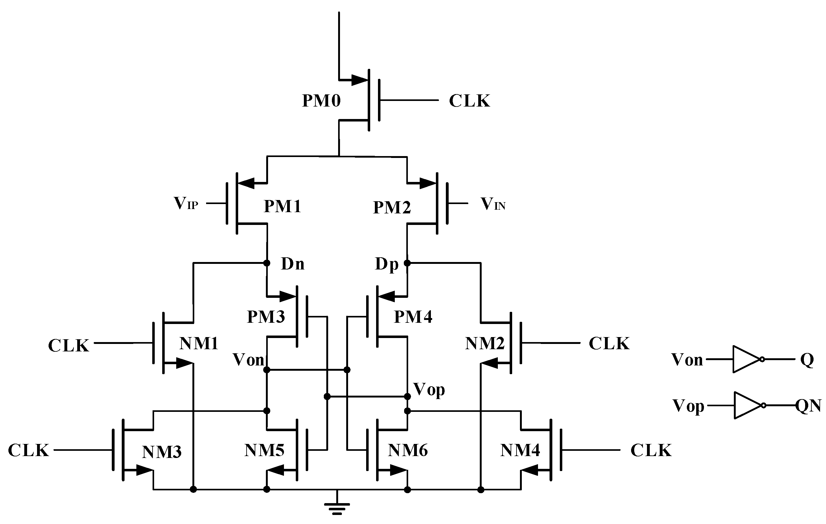
The structure of the comparator combined with the preamplifier and latch can take into account the speed and accuracy, so this structure is used as the comparator in this paper. The strong-arm latch is used in this paper, as shown in Figure 10. When CLK is high, transistor PM0 is off, and transistors NM1–NM4 are on, so Dn, Dp, Von and Vop are pulled to the GND, and the latch is in a reset state. When CLK is low, transistor PM0 is on and transistors NM1–NM4 are off. Von and Vop will be charged at different speeds due to different input voltage signals. If VIP is greater than VIN, the Vop will be charged faster. When the voltage of Vop and Von rises to the threshold voltage, transistors NM5 and NM6 will be switched on, so transistors PM3, PM4, NM5 and NM6 form positive feedback. Due to the faster charging speed of Vop, transistor PM3 will be turned off, and Von will not rise but fall to GND. Vop continues to rise to VDD. The output differential voltage of the latch can be expressed as
where τ is equal to gm/C. It can be seen from (3) that the differential output voltage of the latch increases exponentially, so in the actual working process, the whole process time is very short and can be completed in ns or even ps.
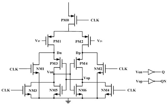
Figure 10.
Schematics of the strong-arm latch.
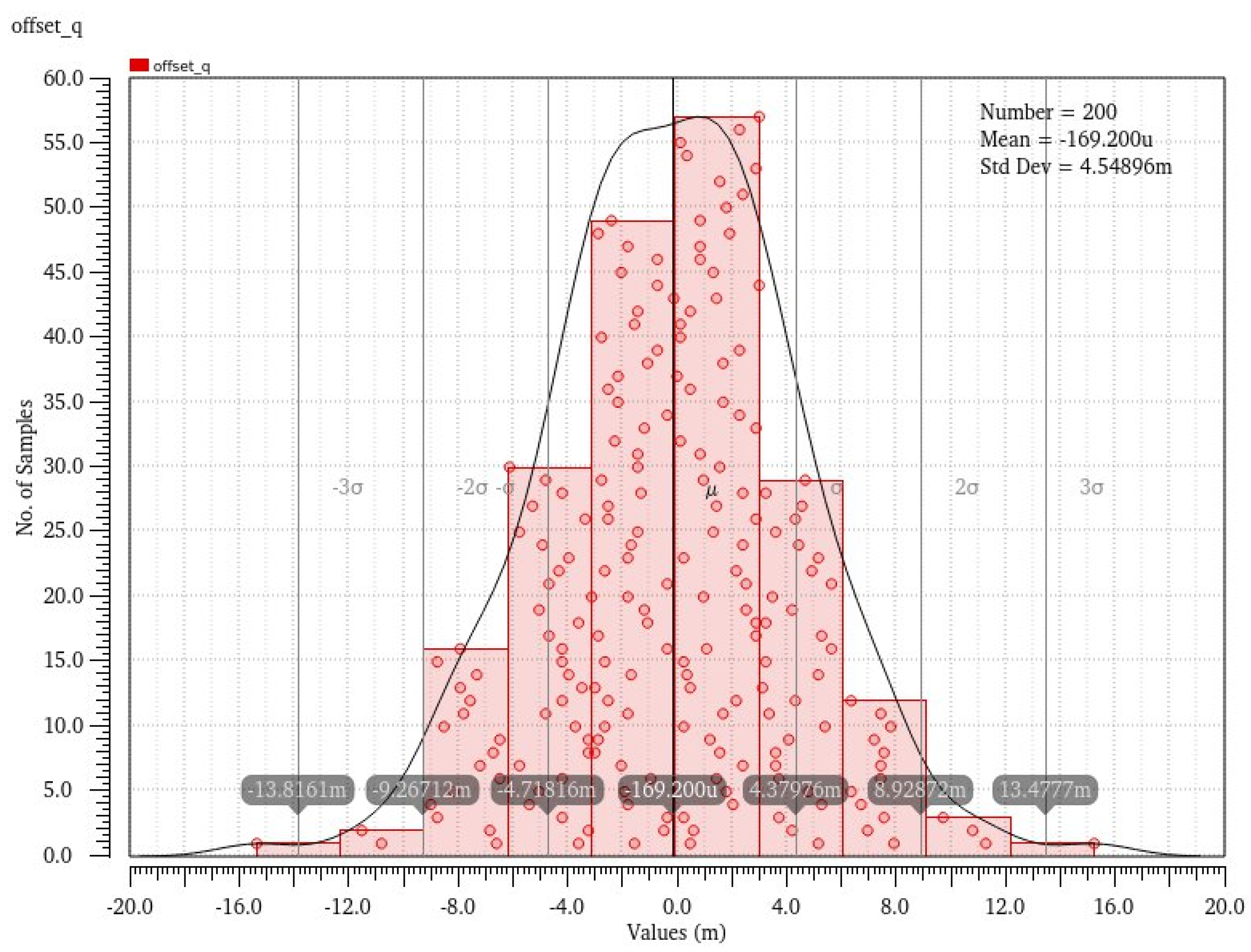
The offset voltage of the strong-arm latch is simulated 200 times by Monte Carlo, and the simulation results are shown in Figure 11. The simulation method is as follows: One end of the comparator inputs VCM and the other end inputs a ramp signal from (VCM − 0.05) V to (VCM + 0.05) V that slowly changes in a small step within the voltage range, observing the output end of the comparator. The voltage difference of the input end when the low level jumps to the high level is the input offset voltage of the comparator. It can be seen that the standard deviation of the offset voltage of the latch is 4.55 mV, so its offset voltage is 13.65 mV. The gain of the preamplifier needs to be high enough to reduce the equivalent input offset voltage of the latch.
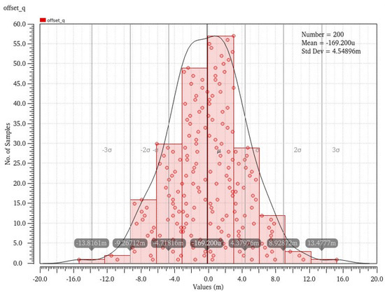
Figure 11.
Monte–Carlo simulation of the strong–arm latch offset.
However, as the output offset storage is DC-coupled, the common-mode input voltage is limited. If the gain of the single-stage preamplifier is too large, the voltage of the capacitance may become saturated. To meet this contradictory demand, the comparator’s structure adopts a combination of a four-stage cascaded preamplifier and a strong-arm latch, as shown in Figure 12. Each preamplifier employs output offset cancellation to further reduce the offset voltage. Taking the first stage preamplifier as an example, its working process is divided into two stages: storage offset voltage stage and normal working stage. In the storage offset voltage stage, the switch S0 is off, and switches CK and CK1 are on. The relationship between the input and output of the preamplifier can be expressed as

Figure 12.
Structure of the comparator with auto-zeroing.
Charges Q1 and Q2 stored on capacitances C1 and C2 (C1 = C2 = C) are
In the working stage, switch S0 is on, and switches CK and CK1 are off. The relationship between the input and output of the preamplifier can be expressed as
Charges Q1 and Q2 on capacitors C1 and C2 are
According to the conservation of charge, the differential output voltage is
It can be seen that the offset voltage is completely eliminated by the stored voltage.
In order to eliminate the charge injection effect caused by switches CK1, CK2, CK3 and CK4 when they are turned off, the switches should be turned off in sequence, as shown in Figure 13, so that the charge injection error generated by the previous switch can be stored on the capacitance and can be eliminated in the normal working stage. Since the comparator is in an idle state during the sampling stage, the offset voltage calibration stage of the comparator and the sampling stage can be combined; that is, the sampling clock not only controls the ADC for sampling but controls the comparator for offset calibration as well.
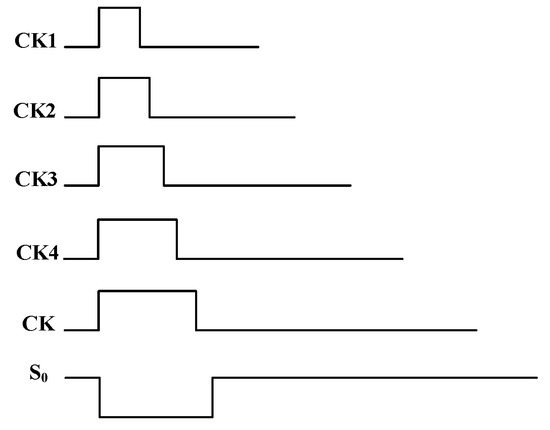
Figure 13.
Timing diagram of the switches.
Figure 14 shows the Monte Carlo simulation result of the designed comparator; the standard deviation of the comparator offset voltage is as low as 4 uV, which meets the design requirements of the 16-bit SAR ADC.
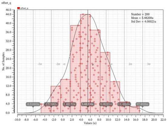
Figure 14.
Monte–Carlo simulation of the comparator offset.
4.4. SAR Logic
The clock generation circuit of this design is shown in Figure 15. GT is a clock control signal, which avoids additional power consumption when the comparator does not generate a clock signal after one conversion is completed. When GT is low, the output signal NCK is low and CKC is high, the comparator is in the reset state, and the comparator outputs Q and QN are high. If GT is high, NCK becomes high, CKC becomes low and the comparator is in operation. After comparison, the levels of Q and QN are opposite, driving NCK down and the comparator into the reset phase. The above procedure is repeated in a cycle to produce an asynchronous clock CKC with alternating levels. The asynchronous clock frequency may vary in different process, voltage and temperature (PVT) conditions. If the frequency is too slow, the entire conversion process may not be completed, and if the frequency is too fast, the DAC may not be fully established, resulting in a comparison error. In this paper, a delay module is used to adjust the asynchronous clock frequency flexibly to ensure that the SAR ADC can work normally under different PVT conditions. The delay module is based on the inverter with adjustable bias, and the discharge current of NMOS in the logic gate is controlled by the external bias current source so as to control the logic delay. Compared with the digital code control, the analog mode adjustment through the bias current is more accurate and the introduction of a long delay chain can be avoided.
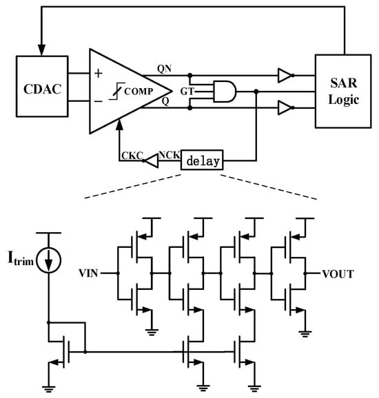
Figure 15.
Schematics of the asynchronous clock generation.
5. Conclusions
This paper has presented a power-efficient 16-bit 1 MS/s SAR ADC in 180 nm CMOS, with a high-precision comparator and a DAC digital foreground calibration. Both a four-stage pre-amplifier and an auto-zeroing technique are applied to achieve 12 μV comparator input offset. The calibration based on low-bit weight improves the ADC’s SNDR and SFDR from 72.56 dB and 78.64 dB to 93.21 dB and 105.1 dB, respectively. The power consumption of the core ADC is 5.4 mW, corresponding to an excellent Schreier figure of merit (FoM) of 175.3 dB.
Author Contributions
Research methodology, X.H.; circuit design, X.H.; calibration algorithm design, W.Q.; layout drawing, X.H.; writing—original draft preparation, X.H.; supervision, X.X. and H.F. All authors have read and agreed to the published version of the manuscript.
Funding
This work was supported and funded in part by the Guangdong Key Area Research and Development Program, China (2019B010143003), and the Shenzhen Science and Technology innovative committee, China (GJHZ20200731095609029).
Data Availability Statement
The original contributions presented in this study are included in the article material. The data presented in this study are available in this paper.
Conflicts of Interest
The authors declare no conflicts of interest.
References
- Liu, J.; Wang, X.; Gao, Z.; Zhan, M.; Tang, X.; Sun, N. 9.3 A 40kHz-BW 90dB-SNDR Noise-Shaping SAR with 4× Passive Gain and 2nd-Order Mismatch Error Shaping. In Proceedings of the 2020 IEEE International Solid-State Circuits Conference-(ISSCC), San Francisco, CA, USA, 16–20 February 2020; pp. 158–160. [Google Scholar]
- Zhu, Y.; Chan, C.H.; Chio, U.F.; Sin, S.W.; Seng-Pan, U.; Martins, R.P.; Maloberti, F. A 10-bit 100-MS/s Reference-Free SAR ADC in 90 nm CMOS. IEEE J. Solid-State Circuits 2010, 45, 1111–1121. [Google Scholar] [CrossRef]
- Bindra, H.S.; Annema, A.J.; Louwsma, S.M.; Nauta, B. A 0.2–8 MS/s 10b flexible SAR ADC achieving 0.35–2.5 fJ/conv-step and using self-quenched dynamic bias comparator. In Proceedings of the 2019 Symposium on VLSI Circuits, Kyoto, Japan, 9–14 June 2019; pp. C74–C75. [Google Scholar]
- Maddox, M.; Chen, B.; Coln, M.; Kapusta, R.; Shen, J.; Fernando, L. A 16 bit linear passive-charge-sharing SAR ADC in 55nm CMOS. In Proceedings of the 2016 IEEE Asian Solid-State Circuits Conference (A-SSCC), Toyama, Japan, 7–9 November 2016; pp. 153–156. [Google Scholar]
- Konno, S.; Miyahara, Y.; Sobue, K.; Hamashita, K. A 16b 1.62MS/s Calibration-free SAR ADC with 86.6dB SNDR utilizing DAC Mismatch Cancellation Based on Symmetry. In Proceedings of the 2020 IEEE Asian Solid-State Circuits Conference (A-SSCC), Hiroshima, Japan, 9–11 November 2020; pp. 1–2. [Google Scholar]
- Cao, C.; Ye, Q.; Zhu, Z.; Yang, Y. A background digital calibration of split-capacitor 16-bit SAR ADC with sub-binary architecture. Microelectron. J. 2015, 46, 795–800. [Google Scholar] [CrossRef]
- Verma, N.; Chandrakasan, A.P. An Ultra Low Energy 12-bit Rate-Resolution Scalable SAR ADC for Wireless Sensor Nodes. IEEE J. Solid-State Circuits 2007, 42, 1196–1205. [Google Scholar] [CrossRef]
- Choi, S.; Ku, H.S.; Son, H.; Kim, B.; Park, H.J.; Sim, J.Y. An 84.6-dB-SNDR and 98.2-dB-SFDR Residue-Integrated SAR ADC for Low-Power Sensor Applications. IEEE J. Solid-State Circuits 2018, 53, 404–417. [Google Scholar] [CrossRef]
- Hsu, C.W.; Chang, S.J.; Huang, C.P.; Chang, L.J.; Shyu, Y.T.; Hou, C.H.; Tseng, H.A.; Kung, C.Y.; Hu, H.J. A 12-b 40-MS/s Calibration-Free SAR ADC. IEEE Trans. Circuits Syst. I Regul. Pap. 2018, 65, 881–890. [Google Scholar] [CrossRef]
- Miki, T.; Morie, T.; Matsukawa, K.; Bando, Y.; Okumoto, T.; Obata, K.; Sakiyama, S.; Dosho, S. A 4.2 mW 50 MS/s 13 bit CMOS SAR ADC With SNR and SFDR Enhancement Techniques. IEEE J. Solid-State Circuits 2015, 50, 1372–1381. [Google Scholar] [CrossRef]
- Yang, C.; Qiu, L.; Tang, K.; Zheng, Y. A 98.6 dB SNDR SAR ADC With a Mismatch Error Shaping Technique Implemented With Double Sampling. IEEE Trans. Circuits Syst. II Express Briefs 2022, 69, 774–778. [Google Scholar] [CrossRef]
- McNeill, J.; Coln, M.C.W.; Larivee, B.J. “Split ADC” architecture for deterministic digital background calibration of a 16-bit 1-MS/s ADC. IEEE J. Solid-State Circuits 2005, 40, 2437–2445. [Google Scholar] [CrossRef]
- Enz, C.C.; Temes, G.C. Circuit techniques for reducing the effects of op-amp imperfections: Autozeroing, correlated double sampling, and chopper stabilization. Proc. IEEE 1996, 84, 1584–1614. [Google Scholar] [CrossRef]
- Razavi, B.; Wooley, B.A. Design techniques for high-speed, high-resolution comparators. IEEE J. Solid-State Circuits 1992, 27, 1916–1926. [Google Scholar] [CrossRef]
- Hesener, M.; Eicher, T.; Hanneberg, A.; Herbison, D.; Kuttner, F.; Wenske, H. A 14b 40 MS/s Redundant SAR ADC with 480 MHz Clock in 0.13 pm CMOS. In Proceedings of the 2007 IEEE International Solid-State Circuits Conference, Digest of Technical Papers, San Francisco, CA, USA, 11–15 February 2007; pp. 248–600. [Google Scholar]
- Allstot, D.J. A precision variable-supply CMOS comparator. IEEE J. Solid-State Circuits 1982, 17, 1080–1087. [Google Scholar] [CrossRef]
- Lee, H.S.; Hodges, D.A.; Gray, P.R. A self-calibrating 15 bit CMOS A/D converter. IEEE J. Solid-State Circuits 1984, 19, 813–819. [Google Scholar] [CrossRef]
- Tseng, W.H.; Lee, W.L.; Huang, C.Y.; Chiu, P.C. A 12-bit 104-MS/s SAR ADC in 28 nm CMOS for digitally-assisted wireless transmitters. In Proceedings of the 2015 IEEE Asian Solid-State Circuits Conference (A-SSCC), Xiamen, China, 9–11 November 2015; pp. 1–4. [Google Scholar]
- Kapusta, R.; Shen, J.; Decker, S.; Li, H.; Ibaragi, E.; Zhu, H. A 14b 80 MS/s SAR ADC With 73.6 dB SNDR in 65 nm CMOS. IEEE J. Solid-State Circuits 2013, 48, 3059–3066. [Google Scholar] [CrossRef]
- Liu, W.; Huang, P.; Chiu, Y. A 12b 22.5/45 MS/s 3.0 mW 0.059 mm2 CMOS SAR ADC achieving over 90 dB SFDR. In Proceedings of the 2010 IEEE International Solid-State Circuits Conference-(ISSCC), San Francisco, CA, USA, 7–11 February 2010; pp. 380–381. [Google Scholar]
- Li, H.; Maddox, M.; Coin, M.C.W.; Buckley, W.; Hummerston, D.; Naeem, N. A signal-independent background-calibrating 20b 1 MS/S SAR ADC with 0.3 ppm INL. In Proceedings of the 2018 IEEE International Solid-State Circuits Conference-(ISSCC), San Francisco, CA, USA, 11–15 February 2018; pp. 242–244. [Google Scholar]
- Murmann, B. ADC Performance Survey 1997–2023. Available online: https://github.com/bmurmann/ADC-survey (accessed on 1 May 2024).
- Shen, J.; Shikata, A.; Fernando, L.D.; Guthrie, N.; Chen, B.; Maddox, M.; Mascarenhas, N.; Kapusta, R.; Coln, M.C.W. A 16-bit 16-MS/s SAR ADC With On-Chip Calibration in 55-nm CMOS. IEEE J. Solid-State Circuits 2018, 53, 1149–1160. [Google Scholar] [CrossRef]
- Xu, H.; Huang, H.; Cai, Y.; Du, L.; Zhou, Y.; Xu, B.; Gong, D.; Ye, J.; Chiu, Y. A 78.5-dB SNDR Radiation- and Metastability-Tolerant Two-Step Split SAR ADC Operating Up to 75 MS/s With 24.9-mW Power Consumption in 65-nm CMOS. IEEE J. Solid-State Circuits 2019, 54, 441–451. [Google Scholar] [CrossRef]
- Zhang, M.; Cao, Y.; Zhu, Y.; Chan, C.H.; Martins, R.P. A 79.5 dB-SNDR Pipelined-SAR ADC with a Linearity-Shifting 32× Dynamic Amplifier and Mounted-Over-Die Bypass Capacitors. In Proceedings of the 2023 IEEE Symposium on VLSI Technology and Circuits (VLSI Technology and Circuits), Kyoto, Japan, 11–16 June 2023; pp. 1–2. [Google Scholar]
- Bannon, A.; Hurrell, C.P.; Hummerston, D.; Lyden, C. An 18 b 5 MS/s SAR ADC with 100.2 dB dynamic range. In Proceedings of the 2014 Symposium on VLSI Circuits Digest of Technical Papers, Honolulu, HI, USA, 10–13 June 2014; pp. 1–2. [Google Scholar]
- Chung, Y.H.; Tien, C.H.; Zeng, Q.F. A 16-Bit Calibration-Free SAR ADC With Binary-Window and Capacitor-Swapping DAC Switching Schemes. IEEE Trans. Circuits Syst. I Regul. Pap. 2022, 69, 88–99. [Google Scholar] [CrossRef]
- Fiorelli, R.; Guerra, Ó.; Río, R.D.; Rodríguez-Vázquez, Á. Effects of capacitors non-idealities in un-even split-capacitor array SAR ADCs. In Proceedings of the 2015 Conference on Design of Circuits and Integrated Systems (DCIS), Estoril, Portugal, 25–27 November 2015; pp. 1–4. [Google Scholar]
- Srinivasan, C.; Godbole, K.M. Error Correction Architecture to Increase Speed and Relax Current Drive Requirements of SAR ADC. U.S. Patent US6747589B2, 8 June 2004. [Google Scholar]
- Liu, C.C.; Chang, S.J.; Huang, G.Y.; Lin, Y.Z.; Huang, C.M.; Huang, C.H.; Bu, L.; Tsai, C.C. A 10b 100 MS/s 1.13 mW SAR ADC with binary-scaled error compensation. In Proceedings of the 2010 IEEE International Solid-State Circuits Conference-(ISSCC), San Francisco, CA, USA, 7–11 February 2010; pp. 386–387. [Google Scholar]
Disclaimer/Publisher’s Note: The statements, opinions and data contained in all publications are solely those of the individual author(s) and contributor(s) and not of MDPI and/or the editor(s). MDPI and/or the editor(s) disclaim responsibility for any injury to people or property resulting from any ideas, methods, instructions or products referred to in the content. |
© 2024 by the authors. Licensee MDPI, Basel, Switzerland. This article is an open access article distributed under the terms and conditions of the Creative Commons Attribution (CC BY) license (https://creativecommons.org/licenses/by/4.0/).

