
Efficient Addition Circuits Using Three-Gate Reconfigurable Field Effect Transistors


Abstract
1. Introduction
2. Background and Related Designs
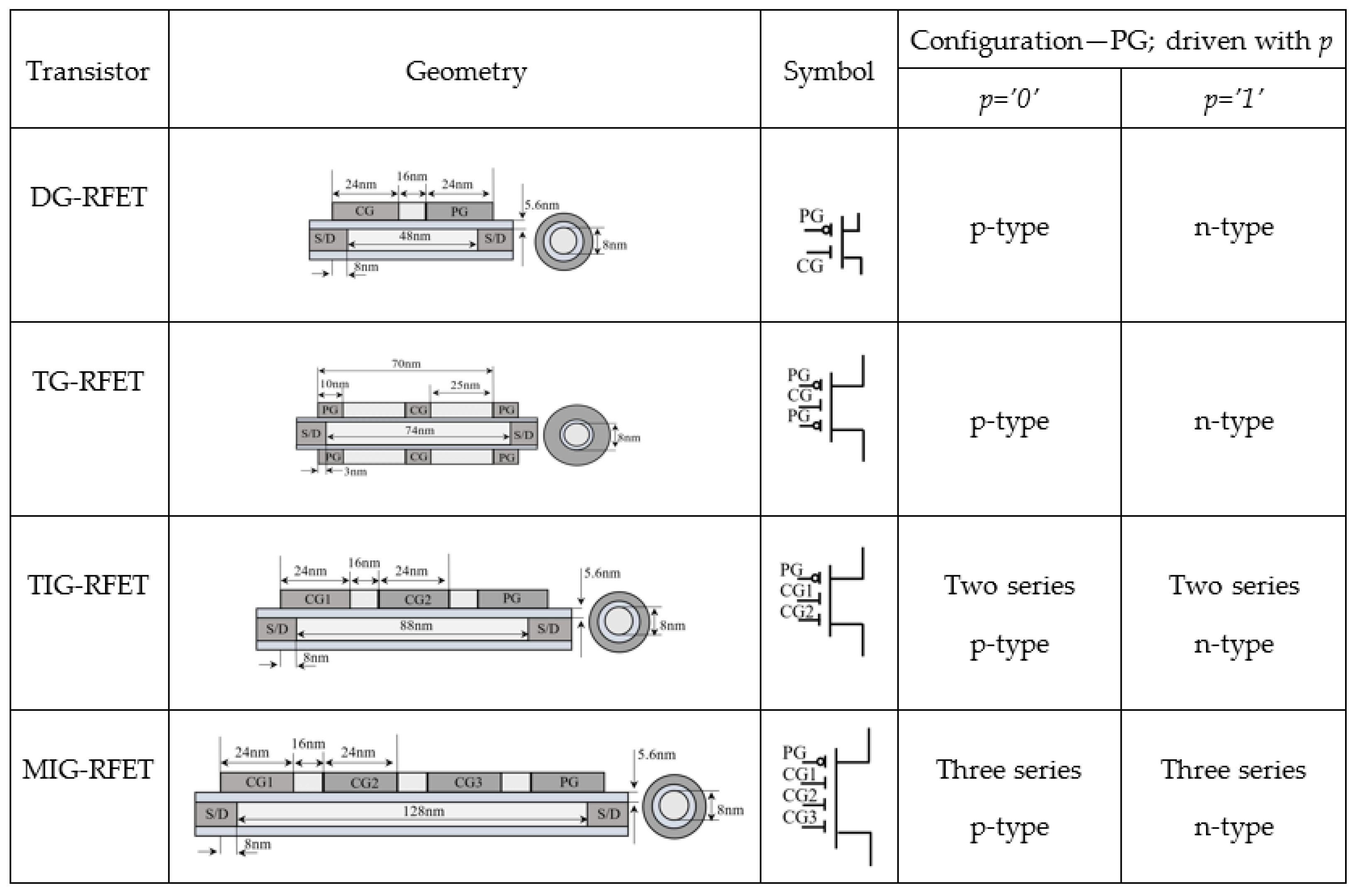
2.1. The Predictive Model Referenced
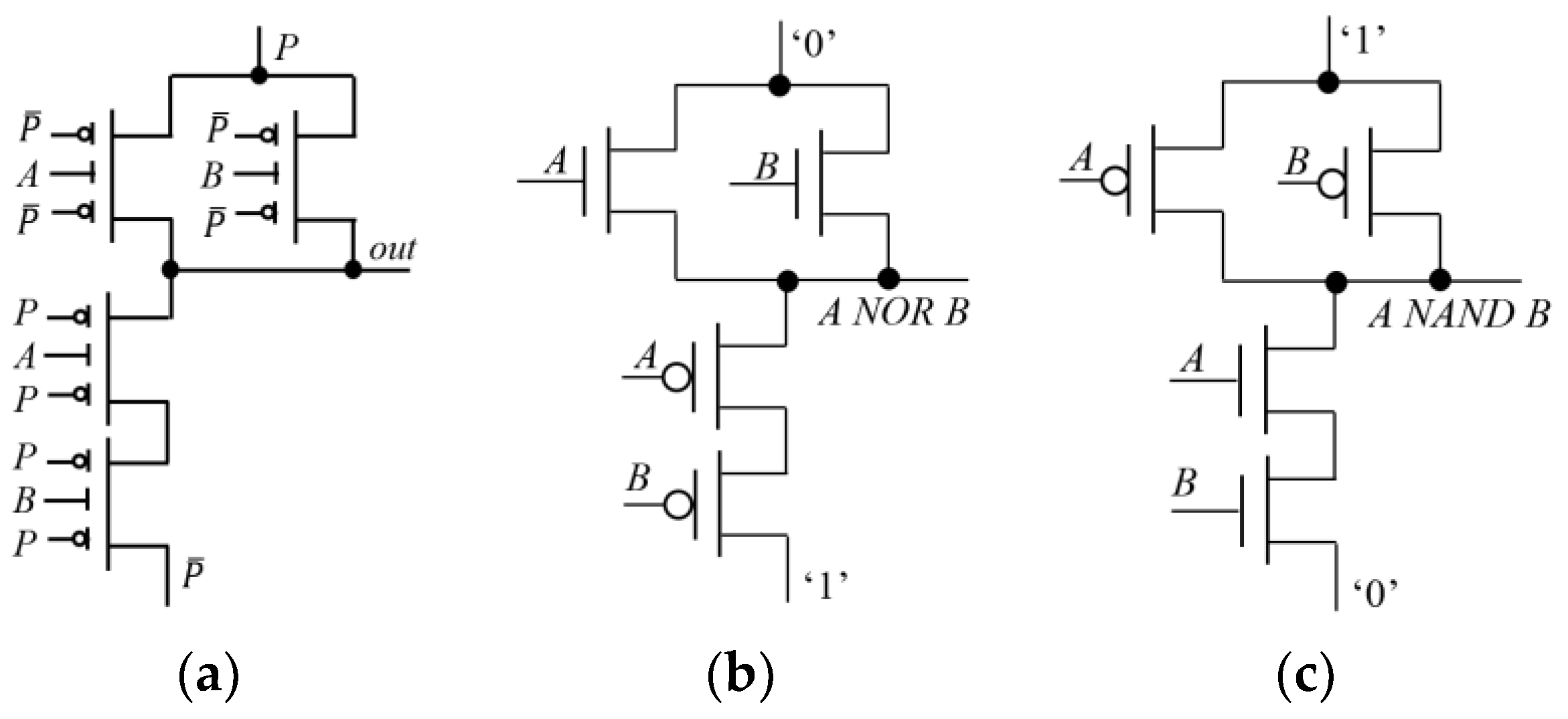
2.2. Sample RFET-Based Digital Circuits
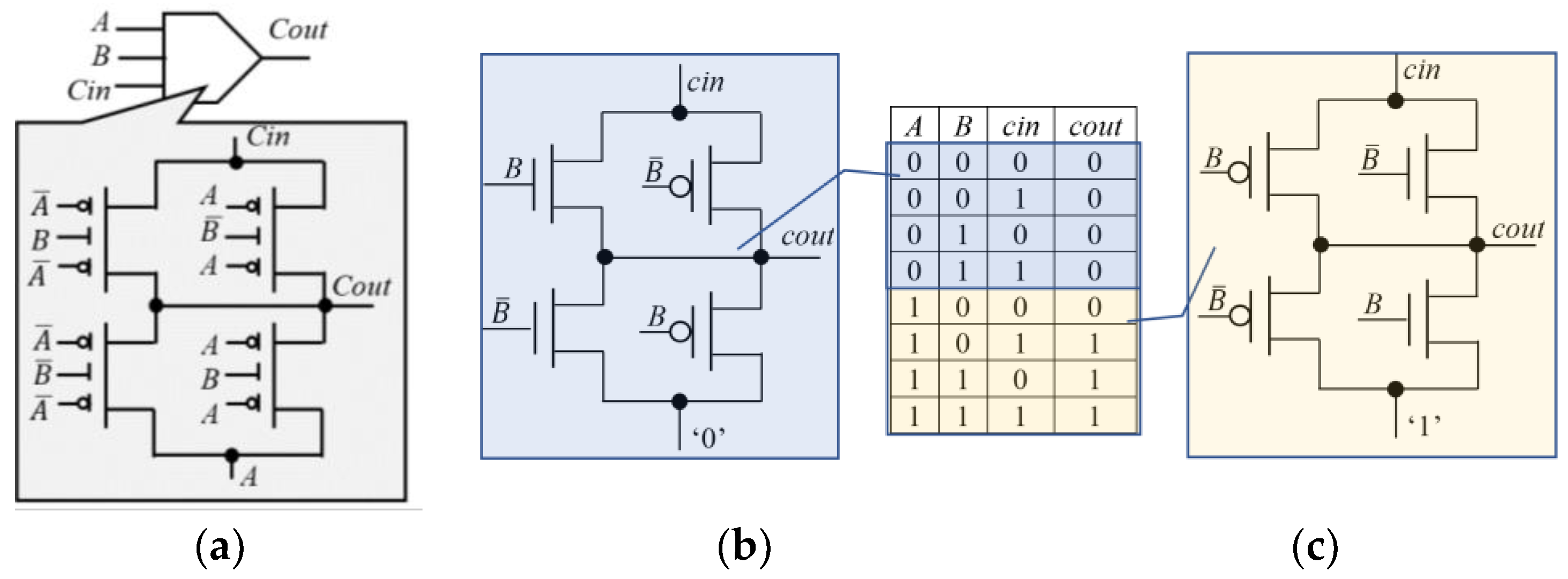
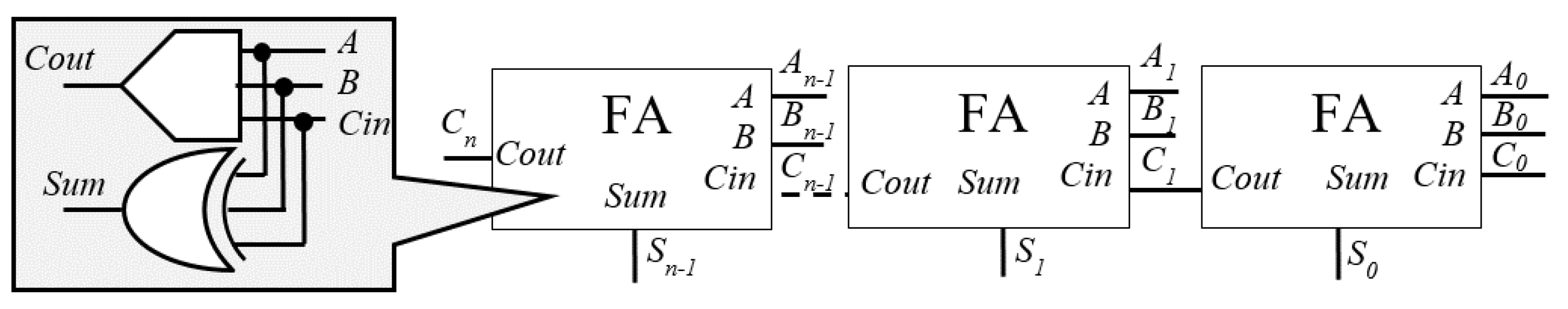
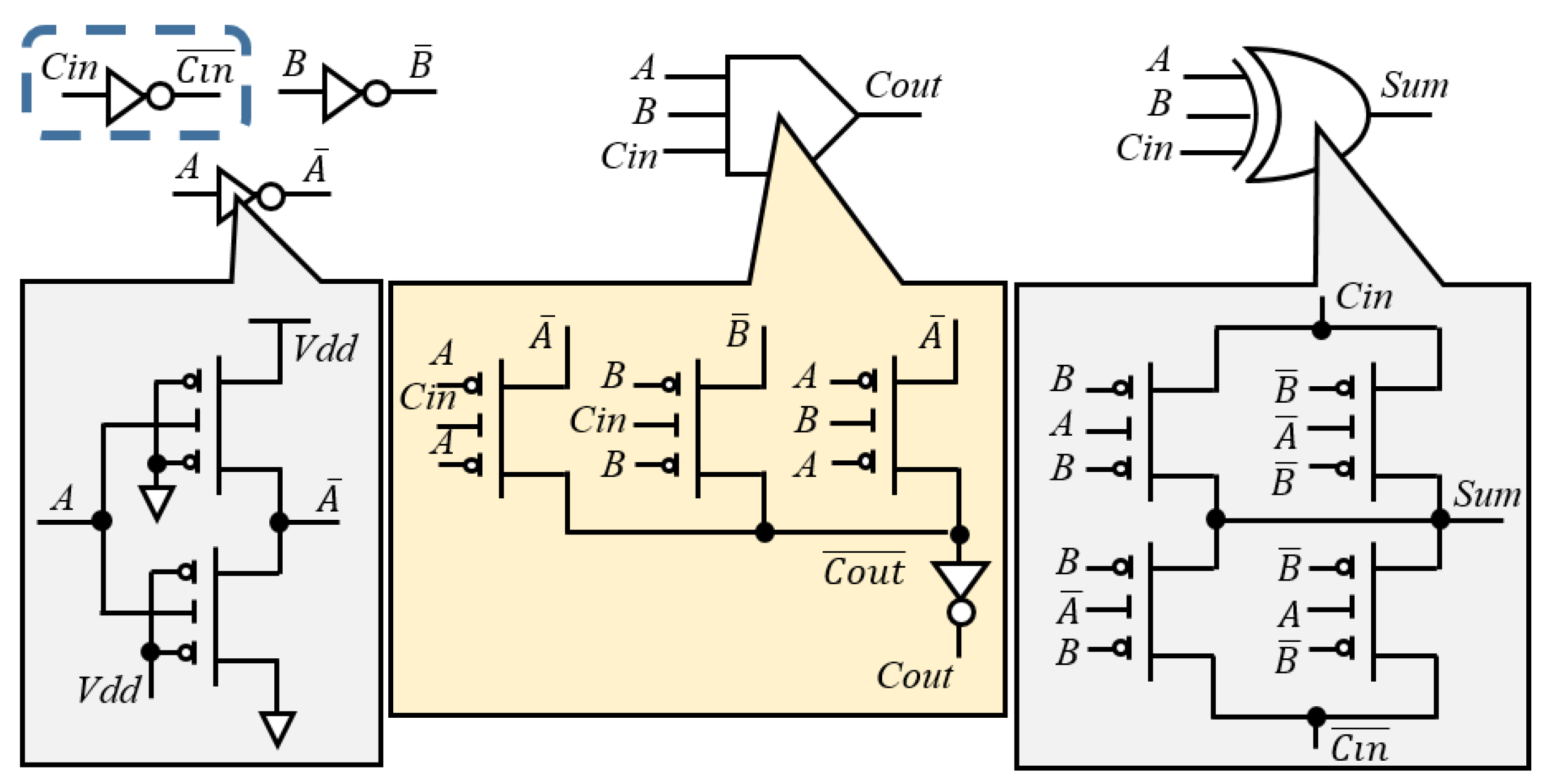
3. The Proposed Designs
4. Conclusions
Author Contributions
Funding
Data Availability Statement
Conflicts of Interest
References
- Bespalov, V.A.; Dyuzhev, N.A.; Yu Kireev, V. Possibilities and Limitations of CMOS Technology for the Production of Various Microelectronic Systems and Devices. Nanobiotechnol. Rep. 2022, 17, 24–38. [Google Scholar] [CrossRef]
- Hutchby, J.A.; Bourianoff, G.I.; Zhirnov, V.V.; Brewer, J.E. Extending the road beyond CMOS. IEEE Circuits Devices Mag. 2002, 18, 28–41. [Google Scholar] [CrossRef]
- Heinzig, A.; Slesazeck, S.; Kreupl, F.; Mikolajick, T.; Weber, W.M. Reconfigurable silicon nanowire transistors. Nano Lett. 2012, 12, 119–124. [Google Scholar] [CrossRef] [PubMed]
- De Marchi, M.; Sacchetto, D.; Frache, S.; Zhang, J.; Gaillardon, P.-E.; Leblebici, Y.; De Micheli, G. Polarity control in double-gate gate-all-around vertically stacked silicon nanowire FETs. In Proceedings of the International Electron Devices Meeting, San Francisco, CA, USA, 10–13 December 2012. [Google Scholar]
- Heinzig, A.; Mikolajick, T.; Trommer, J.; Grimm, D.; Weber, W.M. Dually active silicon nanowire transistors and circuits with equal electron and hole transport. Nano Lett. 2013, 13, 4176–4418. [Google Scholar] [CrossRef] [PubMed]
- Trommer, J.; Heinzig, A.; Baldauf, T.; Mikolajick, T.; Weber, W.M.; Raitza, M.; Völp, M. Reconfigurable Nanowire Transistors with Multiple Independent Gates for Efficient and Programmable Combinational Circuits. In Proceedings of the Design, Automation & Test in Europe Conference & Exhibition (DATE), Dresden, Germany, 14–18 March 2016. [Google Scholar]
- Gore, G.; Cadareanu, P.; Giacomin, E.; Gaillardon, P.-E. A Predictive Process Design Kit for Three-Independent-Gate Field-Effect Transistors. In Proceedings of the IFIP/IEEE International Conference on Very Large Scale Integration (VLSI-SoC), Cuzco, Peru, 6–9 October 2019. [Google Scholar]
- Mikolajick, T.; Galderis, G.; Simon, M.; Rai, S.; Kumar, A.; Heinzig, A.; Weber, W.M.; Trommer, J. 20 Years of reconfigurable field-effect transistors: From concepts to future applications. Solid State Electron. 2021, 186, 108036. [Google Scholar] [CrossRef]
- Sun, B.; Richstein, B.; Liebisch, P.; Frahm, T.; Scholz, S.; Trommer, J.; Mikolajick, T.; Knoch, J. On the Operation Modes of Dual-Gate Reconfigurable Nanowire Transistors. IEEE Trans. Electron Devices 2021, 68, 3684–3689. [Google Scholar] [CrossRef]
- Mikolajick, T.; Galderisi, G.; Rai, S.; Simon, M.; Bockle, R.; Sistani, M.; Cakirlar, C.; Bhattacharjee, N.; Mauersberger, T.; Heinzig, A.; et al. Reconfigurable field effect transistors: A technology enablers perspective. Solid-State Electron. 2022, 194, 108381. [Google Scholar] [CrossRef]
- Quijada, J.N.; Baldauf, T.; Rai, S.; Heinzig, A.; Kumar, A.; Weber, W.M.; Mikolajick, T.; Trommer, J. Germanium Nanowire Reconfigurable Transistor Model for Predictive Technology Evaluation. IEEE Trans. Nanotechnol. 2022, 21, 728–736. [Google Scholar] [CrossRef]
- Böckle, R.; Sistani, M.; Lipovec, B.; Pohl, D.; Rellinghaus, B.; Lugstein, A.; Weber, W.M. A top-down platform enabling Ge based reconfigurable transistors. Adv. Mater. Technol. 2022, 7, 2100647. [Google Scholar] [CrossRef]
- Amarù, L.; Gaillardon, P.-E.; De Micheli, G. Efficient Arithmetic Logic Gates Using Double-Gate Silicon Nanowire FETs. In Proceedings of the IEEE 11th International New Circuits and Systems Conference (NEWCAS), Paris, France, 16–19 June 2013. [Google Scholar]
- Tang, X.; Zhang, J.; Gaillardon, P.-E.; De Micheli, G. TSPC Flip-Flop Circuit Design with Three-Independent-Gate Silicon Nanowire FETs. In Proceedings of the IEEE International Symposium on Circuits and Systems (ISCAS), Melbourne, VIC, Australia, 1–5 June 2014. [Google Scholar]
- Raitza, M.; Kumar, A.; Völp, M.; Walter, D.; Trommer, J.; Mikolajick, T.; Weber, W.M. Exploiting transistor-level reconfiguration to optimize combinational circuits. In Proceedings of the Design, Automation & Test in Europe Conference & Exhibition (DATE), Lausanne, Switzerland, 27–31 March 2017. [Google Scholar]
- Rai, S.; Trommer, J.; Raitza, M.; Mikolajick, T.; Weber, W.M.; Kumar, A. Designing Efficient Circuits Based on Runtime-Reconfigurable Field-Effect Transistors. IEEE Trans. VLSI Syst. 2019, 27, 560–572. [Google Scholar] [CrossRef]
- Sharifi, M.M.; Rajaei, R.; Cadareanut, P.; Gaillardon, P.-E.; Jin, Y.; Niemier, M.; Hu, X.S. A Novel TIGFET-based DFF Design for Improved Resilience to Power Side-Channel Attacks. In Proceedings of the Design, Automation & Test in Europe Conference & Exhibition (DATE), Grenoble, France, 9–13 March 2020. [Google Scholar]
- Galderisi, G.; Mikolajick, T.; Trommer, J. Reconfigurable Field Effect Transistors Design Solutions for Delay-Invariant Logic Gates. IEEE Embed. Syst. Lett. 2022, 14, 107–110. [Google Scholar] [CrossRef]
- Rai, S.; Tempia Calvino, A.; Riener, H.; De Micheli, G.; Kumar, A. Utilizing XMG-Based Synthesis to Preserve Self-Duality for RFET-Based Circuits. IEEE Trans. Comput. Aided Des. Integr. Circuits Syst. 2023, 42, 914–927. [Google Scholar] [CrossRef]
- Kavand, N.; Darjani, A.; Rai, S.; Kumar, A. Design of Energy-Efficient RFET-Based Exact and Approximate 4:2 Compressors and Multipliers. IEEE Trans. Circuits Syst.-II Express Brief 2023, 70, 3644–3648. [Google Scholar] [CrossRef]
- Saravanan, R.; Bavikadi, S.; Rai, S.; Kumar, A.; Dinakarrao, S.M.P. Reconfigurable FET Approximate Computing-based Accelerator for Deep Learning Applications. In Proceedings of the IEEE International Symposium on Circuits and Systems (ISCAS), Monterey, CA, USA, 21–25 May 2023. [Google Scholar]
- Dimitrakopoulos, G.; Papachatzopoulos, K.; Paliouras, V. Sum Propagate Adders. IEEE Trans. Emerg. Top. Comput. 2021, 9, 1479–1488. [Google Scholar] [CrossRef]
- Weste, N.H.E.; Eshraghian, K. Principles of CMOS VLSI Design—A Systems Perspective; Addison-Wesley: Boston, MA, USA, 1993. [Google Scholar]
- Natarajan, S.; Agostinelli, M.; Akbar, S.; Bost, M.; Bowonder, A.; Chikarmane, V.; Chouksey, S.; Dasgupta, A.; Fischer, K.; Fu, Q.; et al. A 14 nm logic technology featuring 2nd-generation FinFET, air-gapped interconnects, self-aligned double patterning and a 0.0588 μm2 sram cell size. In Proceedings of the 2014 IEEE International Electron Devices Meeting, San Francisco, CA, USA, 15–17 December 2014; pp. 3.7.1–3.7.3. [Google Scholar]
- Available online: https://ptm.asu.edu/modelcard/PTM-MG/modelfiles/lstp (accessed on 20 July 2023).


| FA | #FETs | Estimated Area [nm2] | PStatic [W] | Pdyn [W] | Delay [ps] | |||
|---|---|---|---|---|---|---|---|---|
| Sum-AB | Cout-AB | Sum-Cin | Cout-Cin | |||||
| Mirror CMOS | 28 | 11,760 | 1.65 × 10⁻⁶ | 6.25 × 10⁻⁶ | 10.8 | 8.3 | 10.7 | 8 |
| TG-FET [11] | 14 | 14,504 | 1.23 × 10⁻⁹ | 1.55 × 10⁻⁶ | 7.5 | 40.7 | 11 | 28.5 |
| New LSB | 15 | 15,540 | 1.42 × 10⁻⁹ | 1.69 × 10⁻⁶ | 7.7 | 36.6 | 11.7 | 17.1 |
| New NLSB | 13 | 13,468 | 0.84 × 10⁻⁹ | 1.29 × 10⁻⁶ | 7.7 | 36.6 | 10.2 | 16.1 |
| Adder | Tech. | n | #FETs | Estimated Area [nm2] | PStatic [μW] | Edyn [fJ] | Worst-Case Delay [ps] | EDP [J × ps] | |
|---|---|---|---|---|---|---|---|---|---|
| Sn−1-C0 | Cn-C0 | ||||||||
| CMOS * | FinFet | 4 | 112 | 47,040 | 6.32 | 2.1 | 44 | 33 | 92.4 × 10⁻¹⁵ |
| RCA * [11] | TG-FET | 4 | 56 | 58,016 | 4.08 × 10⁻³ | 0.51 | 102.2 | 106.5 | 54.3 × 10⁻¹⁵ |
| NRCA* | TG-FET | 4 | 54 | 55,944 | 3.84 × 10⁻³ | 0.32 | 75.1 | 85.2 | 27.3 × 10⁻¹⁵ |
| CMOS | FinFet | 8 | 224 | 94,080 | 14.09 | 1023 × 10−3 | 67.7 | 64.03 | 6.93 × 10⁻¹⁴ |
| RCA [11] | TG-FET | 8 | 112 | 116,032 | 7.79 × 10⁻³ | 50.86 × 10⁻³ | 302 | 314.5 | 1.60 × 10⁻¹⁴ |
| NRCA | TG-FET | 8 | 106 | 109,816 | 6.9 × 10⁻³ | 15.28 × 10⁻³ | 143.1 | 152.9 | 2.34 × 10⁻¹⁵ |
| CMOS | FinFet | 16 | 448 | 188,160 | 29.52 | 3.9 | 130 | 126.4 | 5.07 × 10⁻¹³ |
| RCA [11] | TG-FET | 16 | 224 | 232,064 | 18.24 × 10⁻³ | 0.57 | 1000 | 1030 | 5.87 × 10⁻¹³ |
| NRCA | TG-FET | 16 | 210 | 217,560 | 15.52 × 10⁻³ | 0.063 | 299.2 | 309.4 | 1.95 × 10⁻¹⁴ |
| CMOS | FinFet | 32 | 896 | 376,320 | 55.52 | 15.03 | 254.7 | 251 | 3.83 × 10⁻¹² |
| RCA [11] | TG-FET | 32 | 448 | 464,128 | 36.76 × 10⁻³ | 5.76 | 3500 | 3670 | 2.11 × 10⁻¹¹ |
| NRCA | TG-FET | 32 | 418 | 433,048 | 30.72 × 10⁻³ | 0.24 | 612.2 | 622.7 | 1.49 × 10⁻¹³ |
Disclaimer/Publisher’s Note: The statements, opinions and data contained in all publications are solely those of the individual author(s) and contributor(s) and not of MDPI and/or the editor(s). MDPI and/or the editor(s) disclaim responsibility for any injury to people or property resulting from any ideas, methods, instructions or products referred to in the content. |
© 2024 by the authors. Licensee MDPI, Basel, Switzerland. This article is an open access article distributed under the terms and conditions of the Creative Commons Attribution (CC BY) license (https://creativecommons.org/licenses/by/4.0/).
Share and Cite
Spagnolo, F.; Corsonello, P.; Frustaci, F.; Perri, S. Efficient Addition Circuits Using Three-Gate Reconfigurable Field Effect Transistors. J. Low Power Electron. Appl. 2024, 14, 24. https://doi.org/10.3390/jlpea14020024
Spagnolo F, Corsonello P, Frustaci F, Perri S. Efficient Addition Circuits Using Three-Gate Reconfigurable Field Effect Transistors. Journal of Low Power Electronics and Applications. 2024; 14(2):24. https://doi.org/10.3390/jlpea14020024
Chicago/Turabian StyleSpagnolo, Fanny, Pasquale Corsonello, Fabio Frustaci, and Stefania Perri. 2024. "Efficient Addition Circuits Using Three-Gate Reconfigurable Field Effect Transistors" Journal of Low Power Electronics and Applications 14, no. 2: 24. https://doi.org/10.3390/jlpea14020024
APA StyleSpagnolo, F., Corsonello, P., Frustaci, F., & Perri, S. (2024). Efficient Addition Circuits Using Three-Gate Reconfigurable Field Effect Transistors. Journal of Low Power Electronics and Applications, 14(2), 24. https://doi.org/10.3390/jlpea14020024