Article

BFT—Low-Latency Bit-Slice Design of Discrete Fourier Transform

Department of Electrical and Information Engineering, Politecnico di Bari, Via E. Orabona, 4, 70125 Bari, Italy
*
Authors to whom correspondence should be addressed.
J. Low Power Electron. Appl. 2023, 13(3), 45; https://doi.org/10.3390/jlpea13030045
Submission received: 22 June 2023 / Revised: 12 July 2023 / Accepted: 14 July 2023 / Published: 18 July 2023

Abstract

:
Structures for the evaluation of fast Fourier transforms are important components in several signal-processing applications and communication systems. Their capabilities play a key role in the performance enhancement of the whole system in which they are embedded. In this paper, a novel implementation of the discrete Fourier transform is proposed, based on a bit-slice approach and on the exploitation of the input sequence finite word length. Input samples of the sequence to be transformed are split into binary sequences and each one is Fourier transformed using only complex sums. An FPGA-based solution characterized by low latency and low power consumption is designed. Simulations have been carried out, first in the Matlab environment, then emulated in Quartus IDE with Intel. The hardware implementation of the conceived system and the test for the functional accuracy verification have been performed, adopting the DE2-115 development board from Terasic, which is equipped with the Cyclone IV EP4CE115F29C7 FPGA by Intel.

1. Introduction

The adoption of the discrete Fourier transform (DFT) is widespread in digital-signal-processing systems. The DFT maps the time-domain sequence to the frequency-domain sequence of the same length, with a computational cost proportional to N 2 for a DFT of length N. The fast Fourier transform (FFT) algorithm is generally used to effectively perform the DFT so as to partition the whole procedure into smaller procedures [1].
The field of applications of FFT is very broad and diversified, and new uses are surfacing. There is no question that FFT plays a crucial role in several applications, such as audio/speech processing and recognition [2]. Moreover, it is a relevant functional block in modern digital communication systems, for applications in orthogonal frequency-division multiplexing (OFDM) systems [3,4], such as digital worldwide interoperability for microwave access, wireless metropolitan-area networks, and in the areas of next-generation wireless systems, radar signal processing, spectra sensing of cognitive radio, etc. FFT is also used in medical imaging for image filtering, analysis, and image reconstruction [5,6].
Various algorithms have been developed to perform the software version of FFT to maximize the execution time and reduce the computational complexity [7]. Instructions of these procedures are generally executed serially, and, as a result, their execution speed is heavily bound by processor throughput. Hardware implementation of FFT approaches is still a challenging issue, even if it is useful for real-time and high-speed processing. Several architectures for the hardware design of FFT have been suggested in the literature over the years [8,9]. They vary from fully parallel structures with high throughput, low latency, and a significant number of processing elements, to sequential structures with few processing elements and nonoptimized computation times. The basic aim of hardware designers is to achieve cost-effective implementations in terms of high performance, low hardware resource utilization, high accuracy, and low power consumption. Array architectures consisting of a certain number of independent processing elements, with local buffers connected through a network, are characterized by their high performance because of spatial parallelism, but are hardware-consuming and require further routing resources. Spatial development of these structures becomes impractical as the size increases because of the area and power commitments related to the presence of complex interconnections [9,10]. Pipeline architectures are a proper choice for high throughput and real-time applications. The flexibility of these regular architectures indicates an excellent potential for seeking more efficient designs [8]. To achieve better hardware efficiency, memory-based architectures are generally used. They pass data multiple times through either a single butterfly processing element or a set of processing elements, with several memory banks to hold intermediate results. Nevertheless, the throughput of memory-based FFTs is usually restricted by butterfly radix and concurrent data-access contentions [11].
Hardware implementation of FFT procedures can be performed by adopting integrated circuits, such as field-programmable gate arrays (FPGAs) and application-specific integrated circuits (ASICs), which are similar in their circuit designs because logic functions, which are yet to be synthesized, are specified using hardware description languages. FPGA circuits are preferred because of their specific-purpose circuits, low cost, and reconfigurable characteristics (which have architectural flexibility and fast development times) when new functionalities are added [12]. The FPGA design of FFT is often customized to achieve higher speeds on low-power specifications since FPGAs have risen in capacity and performance and reduced in cost.
Several FPGA-based architectures are indicated in the literature for the design of circuits that are able to produce the FFT. Some studies have focused on FFT designs that achieve a trade-off between accuracy and performance by making a bit-width selection during each computational stage [13]. Two different procedures for word-length modification under a specific error margin have been proposed. They perform an approximated FFT evaluation, with the aim of implementing an area-limited design and a high operating frequency. The authors verified that those results without significant losses in quality are reached by applying these strategies to speech recognition when an appropriate word-length combination is achieved for all stages. Furthermore, a word-length adjustment strategy is used in [14] for the design of an FFT processor that can support up to 128k point operations. A fixed-point number design scheme is selected to reduce the requirements in terms of chip memory and logic resources, while still providing real-time performance of data processing. Improvements in efficiency are obtained in [15] by increasing the throughput per logic cell through the design of a circuit characterized by a high clock speed and a reduced number of clock cycles for FFT evaluation. The implemented structure has a systolic distributed-memory-based architecture, which was designed by adopting a true space–time mapping tool to obtain an optimal latency solution.
Approximate arithmetic computation appears to be an effective solution for systems that exhibit an intrinsic error tolerance. In fact, in [16], a reduction in power consumption and in number of logic slices is obtained by adopting energy-efficient approximate multipliers and adders in the butterfly kernel. Furthermore, a low-power and reduced-area FPGA, a reconfigurable fixed-point implementation of FFT/IFFT, is indicated by Nori et al. [17]. A good trade-off among area occupancy, power consumption, and throughput was obtained in [18] by adopting arithmetic-optimization techniques and complex approximate multipliers for the radix-2 butterflies implementation. Approximate half adders, approximate full adders, and approximate compressors are used for designing 8- and 16-point FFT/IFFT core processors that are suitable for multiple inputs and multiple outputs for orthogonal-frequency-division-multiplexing-based applications. Two CORDIC-based FFT/IFFT processors, which adopt one butterfly unit and are based on radix-2 and radix-4 architecture are designed. An in-place memory assignment is used for reducing the memory scheme complexity. Furthermore, an in-place architecture for computing the FFT of real-valued biosignals is indicated in [19] and compared with a fully pipelined, single-processing-element-based architecture for the FFT evaluation through the decimation in time radix-2 algorithm.
A multiplication-free design of an efficient FFT architecture based on the radix-2 decimation in frequency method is indicated in [20]. The complex twiddle factors are replaced by the uniform Montgomery algorithm, which performs shift/addition operations instead of multiplications. A reduction in adders at the price of growth in the memory elements (as compared to the single-path delay feedback) characterizes the single-stream FPGA-optimized feedforward architecture conceived in [21], which performs the FFT through a radix-2 pipeline architecture. The authors outlined that their structure is suitable for FPGA implementation in short-pipeline FFT processors. A comparison among three pipelined FFT architectures, which implement radix-8, radix-4 single-path feedback and radix-4 single-path delay commutator, is indicated in [22]. The choice of which structure to adopt depends on the most strict requirement that needs to be meet. In fact, radix-4 single-path delay commutator is characterized by the lowest use of logical elements and memory bits, while radix-8 structure has the lowest average thermal power dissipation. Conversely, Zhang et al. [23] designed a hybrid architecture with a control unit that configures the processor as a pipeline structure when the FFT point is less than or equal to 512 and as an iterative structure that can support maximum 4096-point FFT operations in case of a number of points greater than 512.
A complete performance comparison of different HW structures is very difficult due to many specific parameter choices, such as the number of samples of the input sequence, the specific HW implementation, the approach for computation units, the recourse to FPGA or DSP, whether floating or fixed point, and whether the architecture of the HW structure as pipeline, sequential, etc.
In this paper, a novel approach is presented for the DFT computation. Our method exploits the finite word-length precision of the input sequence by splitting input sequence samples into bit slices and applying the DFT to each bit slice. The computation is thereby simplified because only complex sums are required instead of complex multiples. Each bit slice can be carried out in a time-sequential approach with a low-cost system. With this architecture, the output values of the evaluated transform accumulate and update the partial results until the last sample of the sequence is acquired. The conceived architecture is a low-latency solution, which is very useful in many demanding technology systems like in 5G communication systems for very low-latency applications, like in “smart roads” applications, smart electric utility grids, and industrial automation systems. Furthermore, in general, it can be usefully adopted in real-time applications where latency is a crucial aspect limiting the system performance. In this work, a low-power hardware solution is synthesized, which is based on FPGA device.
The rest of the paper is organized as follows. In Section 2, a summary of DFT/FFT characteristics is indicated. Section 3 deals with the definition of the binary DFT, while in Section 4 the designed architecture is indicated. Section 5 presents the hardware implementation of the FPGA-based solution for the BFT computation in an orthogonal frequency-division multiplexing (OFDM) system, underlining its specificity and usefulness for 5G telecommunications systems. Section 8 completes the paper.

2. DFT/FFT Algorithm: A Brief Overview
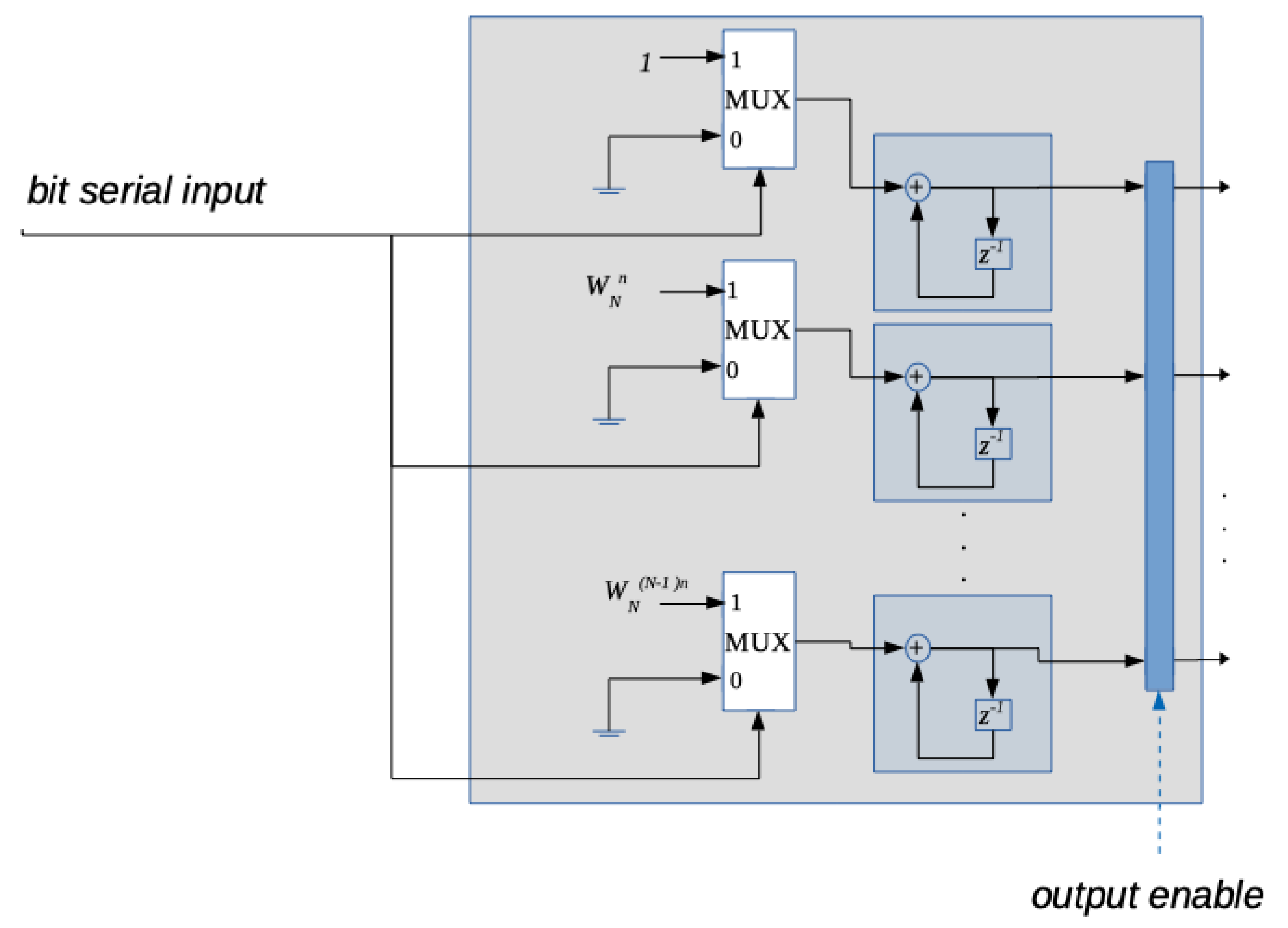
The DFT of a sampled time-domain signal is described by:
X k = n = 0 N 1 x n · W N k n k = 0 , 1 , , N 1
where x n is the n-th time sample, X K represents the DFT frequency output at the k-th spectral point, N is the number of sample points in the DFT data frame, and
W N = e j 2 π N
is the twiddle factor, which is a complex value.
Conceptually, the DFT performs complex matrix multiplication. Stated X ¯ = [ X ( 0 ) , X
( 1 ) , , X ( N 1 ) ] T , the DFT-transformed complex-output vector, and x ¯ = [ x ( 1 ) , x ( 2 ) , , x ( N
1 ) ] T , the input time-domain vector, the DFT is represented by the matrix product:
X = D N · x
where the matrix D N is
D N = 1 1 1 . . . 1 1 W N W N 2 . . . W N N 1 1 W N 2 W N 4 . . . W N 2 ( N 1 ) . . . . . . . . . . . . . . . . . . . . . 1 W N N 1 W N N 2 . . . W N
To reduce the computation complexity of the DFT, a family of algorithms has been developed, named FFT. FFT algorithms are based on the mathematical properties of the matrix D N . They partition the calculation of an N-sample-long DFT into smaller DFTs by applying the strategy of divide and conquer [24]. Depending on the way the DFT is mapped into subproblems, several algorithms have been conceived. Among them are the popular Cooley–Tukey and prime-factor algorithms [25].
In this paper, the limited bit word length of the coefficients of the sequence to be transformed is exploited, instead of exploiting the intrinsic symmetries of matrix D N .

3. The Binary DFT

Let x n be a complex number. Its most general finite precision representation can be expressed as
x n = l = M 1 M 2 1 [ x ( r ) n , l + j · x ( i ) n , l ] · 2 l
where x ( r ) and x ( i ) represent real and imaginary parts of the complex number, respectively, while b is the number of bits used to encode each sample. In detail, M 1 is the number of bits used to represent the fractional part of each sample, while M 2 is its integer part; clearly, M 2 = b M 1 1 .
In the rest of the paper, the hypothesis that the real sequence is assumed as the generalization to the complex case is straightforward.
In the stated simplified hypothesis, by a simple substitution of Equation (5) in Equation (1) we have
X k = n = 0 N 1 l = M 1 M 2 1 x n , l · 2 l · W N k n k = 0 , 1 , , N 1
and hence
X k = l = M 1 M 2 1 2 l n = 0 N 1 x n , l · W N k n k = 0 , 1 , , N 1
If we denote with l-th bit slice in the following set of samples with B S l = ( x 0 , l , x 1 , l , …, x N 1 , l ) with l = M 1 , , M 2 1 , the DFT of the l-th bit slice is defined as
X k , l = n = 0 N 1 x n , l · W N k n k = 0 , , N 1
It is evident from Equation (7) that the computation of the k-th Fourier transform coefficient can be obtained by calculating separately the DFT of each bit slice and adding these partial results weighted by a proper power of two.
Since the generic x n , l value is either zero or one, the DFT slice coefficients result in the sum of all the W N k n vectors at which a bit slice sample equal to one occurs.
We denote the DFT of bit slides with binary DFT (BFT). The BFT evaluation for the generic bit slice through expression (8) can be simplified by exploiting the symmetry properties of kernel values. In Figure 1, an example of the complexity reduction that could happen is indicated for an eight-point BFT slice. A bit slice of eight bits is the input of the computation for a chosen k value. Considering the complex Gauss plane, twiddle factors are represented as vectors and bits set to one sum up to define the BFT value for the specific k. Opposite values give a zero contribution to the sum so that a simplification stage can be proposed to reduce the computational load of the BFT evaluation.

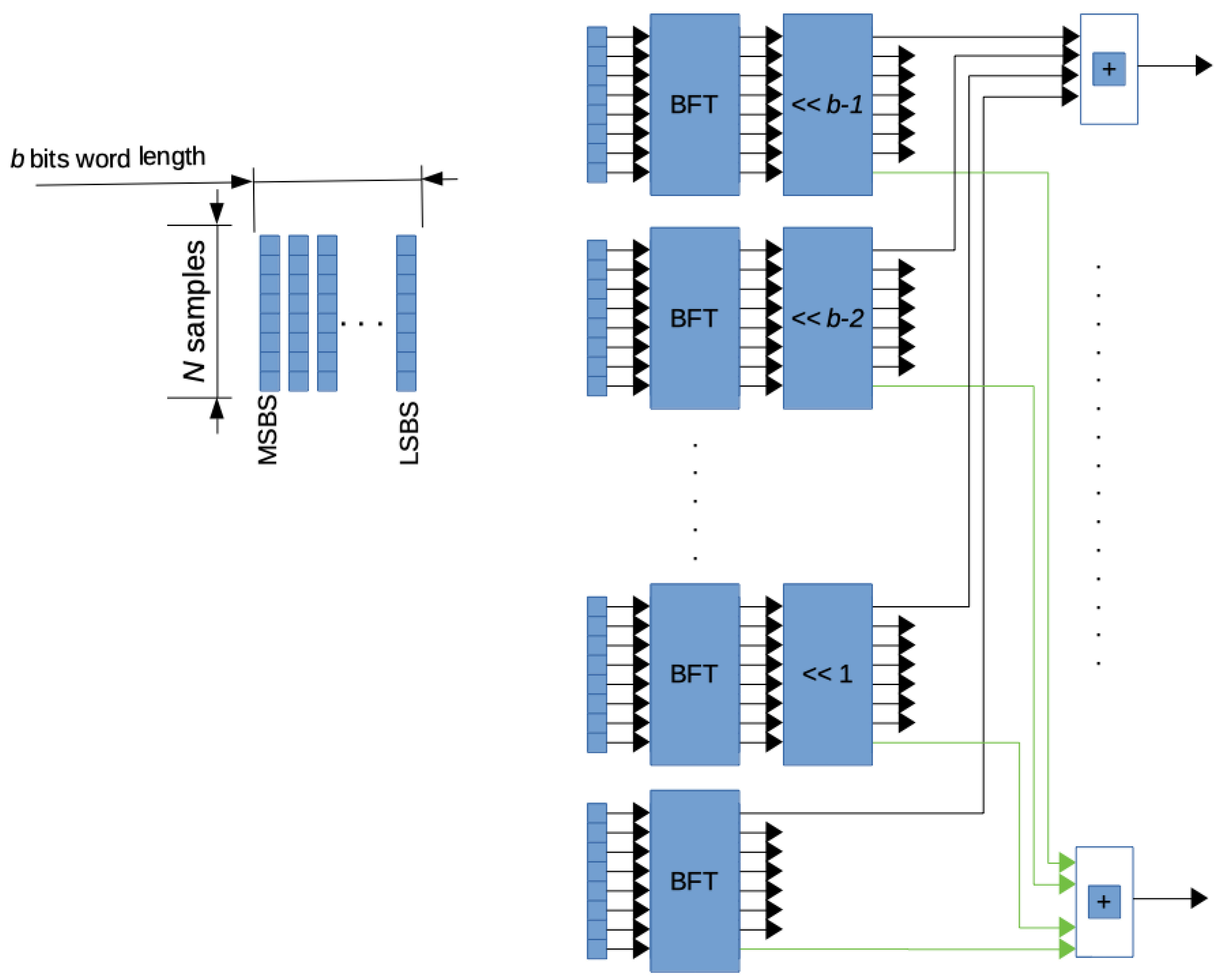
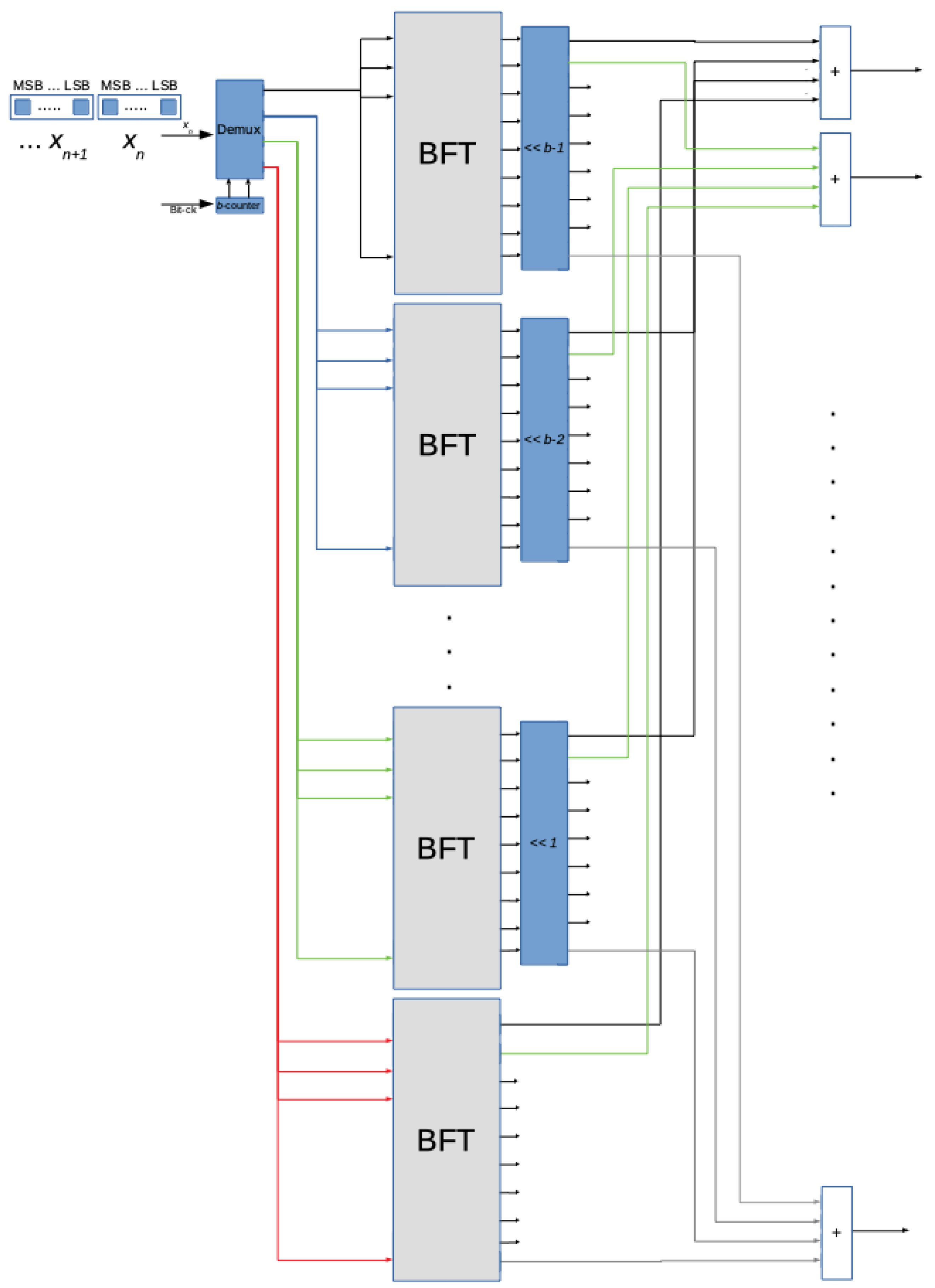
4. Functional Blocks of the Proposed System

The aim of this design is a low-latency hardware implementation suitable for real-time applications, such as high-efficiency numerical transmission systems and signal processing applications.
The diagram of functional blocks composing our structure is shown in Figure 2. Memory devices (such as PISO registers) produce possible series to parallel conversion of inputs.
It is a parallel architecture whose inputs and outputs are the bit slices and the DFT of the N-samples-long sequence, respectively. Each bit slice is processed with a BFT block. Therefore, all the N samples of the input sequence need to be collected and arranged in bit slices for the proper operation of the BFT block. Given that the authors seek to design a low-latency arrangement, an improved solution has been synthesized (Figure 3). In this circuit, the data processing is performed as soon as samples are provided in input. It follows that the collection of all the N samples composing the sequence before starting data processing is not required. As a result, the DFT is obtained a few clock pulses after the last sample of the input sequence has been collected.
The proposed DFT architecture is composed of four functional modules: the DEMUX block, the BFT block, the left-shift block, and the adder block.

4.1. The DEMUX Block

The DEMUX block is a data-distributor device composed of one input and b outputs. Input data are switched to any one of output lines based on the boolean value of the selection variables. These variables are outputs of a modulus b counter provided with a ripple carry output, too.

4.2. The BFT Block

Each BFT block has N inputs and N outputs. Let B F T l be the generic block composing the system, with l [ 0 , b 1 ] . The set of samples composing the l-th bit slice are inputs, while the DFTs of the l-th bit slices are outputs. The block performs all the operations indicated in expression (8).
The logical scheme in Figure 4 shows some details of this block. In particular, the output enabled is the ripple carry output of a modulus N counter, having the ripple carry output of the modulus b counter as count-enabled.
Figure 3. Diagram of functional blocks composing the low − latency solution.
Jlpea 13 00045 g003

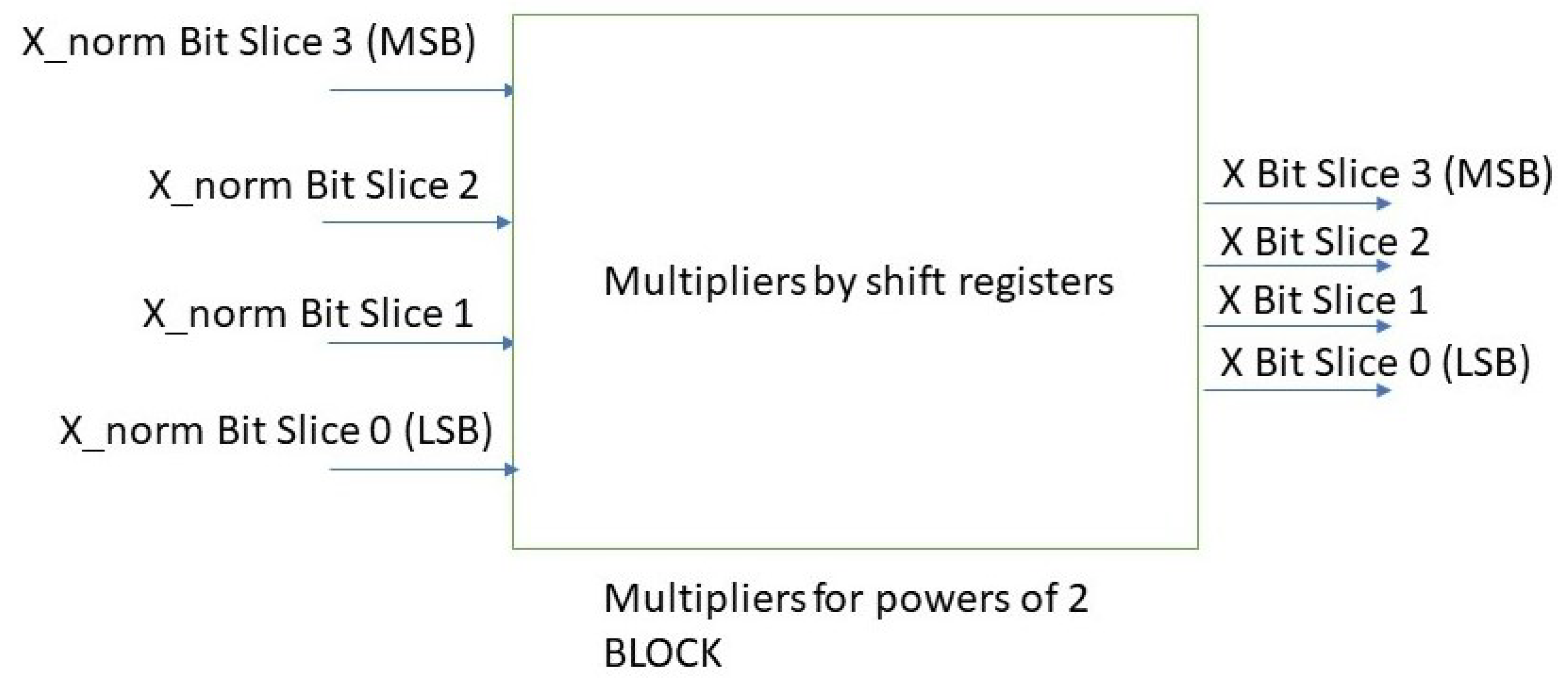
4.3. The Left-Shift Block

The aim of this block is multiplication by a power of two. It is implemented by a left shift. Therefore, the multiplication for the term 2 l can be performed by a shift to the left by l positions. It is evident that ( b 1 ) different blocks are necessary because ( b 1 ) are the multiplications to be carried out, as given by expression (7).

4.4. The Adder Block

The output of this block is the evaluation of one Fourier transform coefficient. For this reason, N blocks are required. The generic k-th block makes possible the computation of the k-th Fourier coefficient by adding the k-th Fourier coefficients of each bit slice weighted by a suitable power of two.
Figure 4. Logical scheme of a generic BFT block having samples of a bit slice as serial inputs.
Jlpea 13 00045 g004

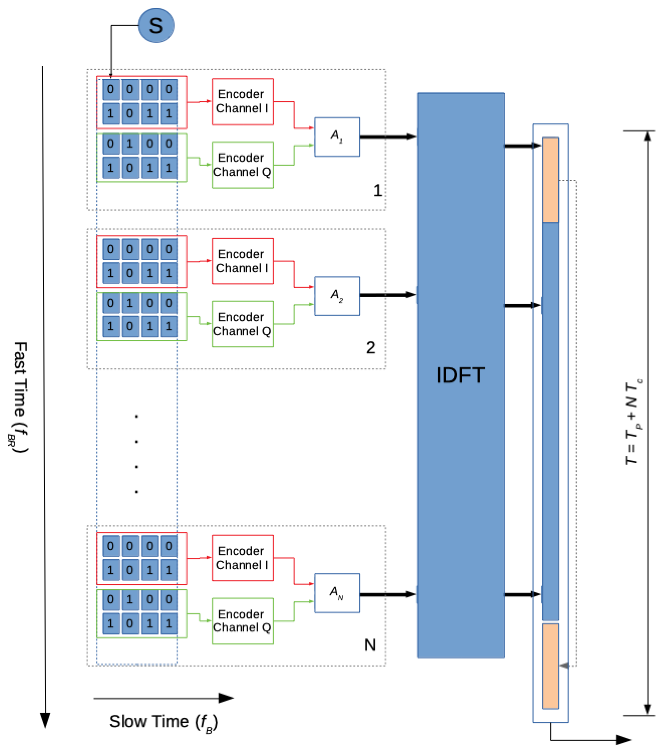
5. Hardware Architecture of the FPGA-Based System: An Application Example

5.1. OFDM Technique Characteristics

The designed architecture for the DFT computation is applied to the OFDM technique, which is used in several digital wireless applications, including digital video broadcasting, digital audio broadcasting, and wireless local-area networks. In fact, the OFDM technique mitigates delay-spread effects and produces high spectral efficiency. It is a multicarrier transmission in which a single data stream is transmitted over several lower-rate subcarriers, which are orthogonal to each other. Each subcarrier is modulated with a conventional digital-modulation scheme, such as quadrature amplitude modulation (QAM). DFT is used to modulate and demodulate the data constellations on the orthogonal subcarriers [26,27,28].
The authors have simulated and implemented the circuit for the DFT evaluation in case of digital video broadcasting—second generation terrestrial (DVB-T2) for the 1 k mode using the 16-QAM constellation of the payload data. The finite word length of the input signal is composed of four bits: two for the in-phase component (I) and two for the in-quadrature component (Q). In Figure 5, the scheme for the 16-QAM modulation is illustrated. In particular, f B R is the bit rate, f B represents the baud rate, T is the symbol length, and T P is the cyclic preamble length. T C is the sampling step, N is the number of carriers (samples), and A i is the i-th complex amplitude of the OFDM payload subcarrier. The IDFT block generates the symbol to be transmitted while the cyclic preamble enables symbol synchronization and allows dealing with multipath and performing channel equalization at the receiver end.

5.2. The Proposed FPGA-Based Architecture

The design purpose is the achievement of a hardware implementation for real-time applications. A solution characterized by low power consumption and minimum hardware resources requirements is also developed.
Fixed-point arithmetic is adopted for data processing. The implemented procedure operates in real time. The FPGA has a time resolution of 1 p s and the chosen clock is 1 n s with a duty cycle of 0.5 .
The block diagram of our system is indicated in Figure 6. It is composed of three modules: the timing block, the ROM block and, the sum/multiplier block.

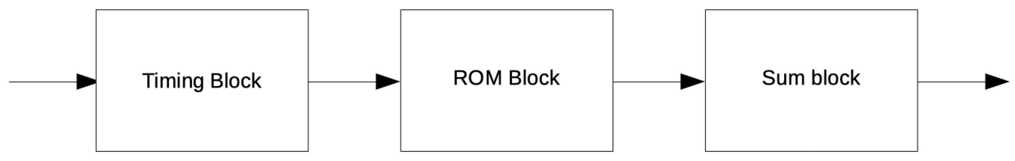
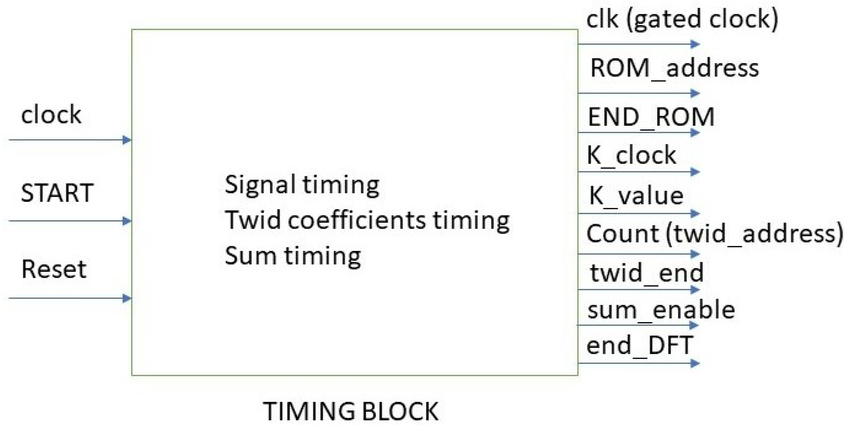
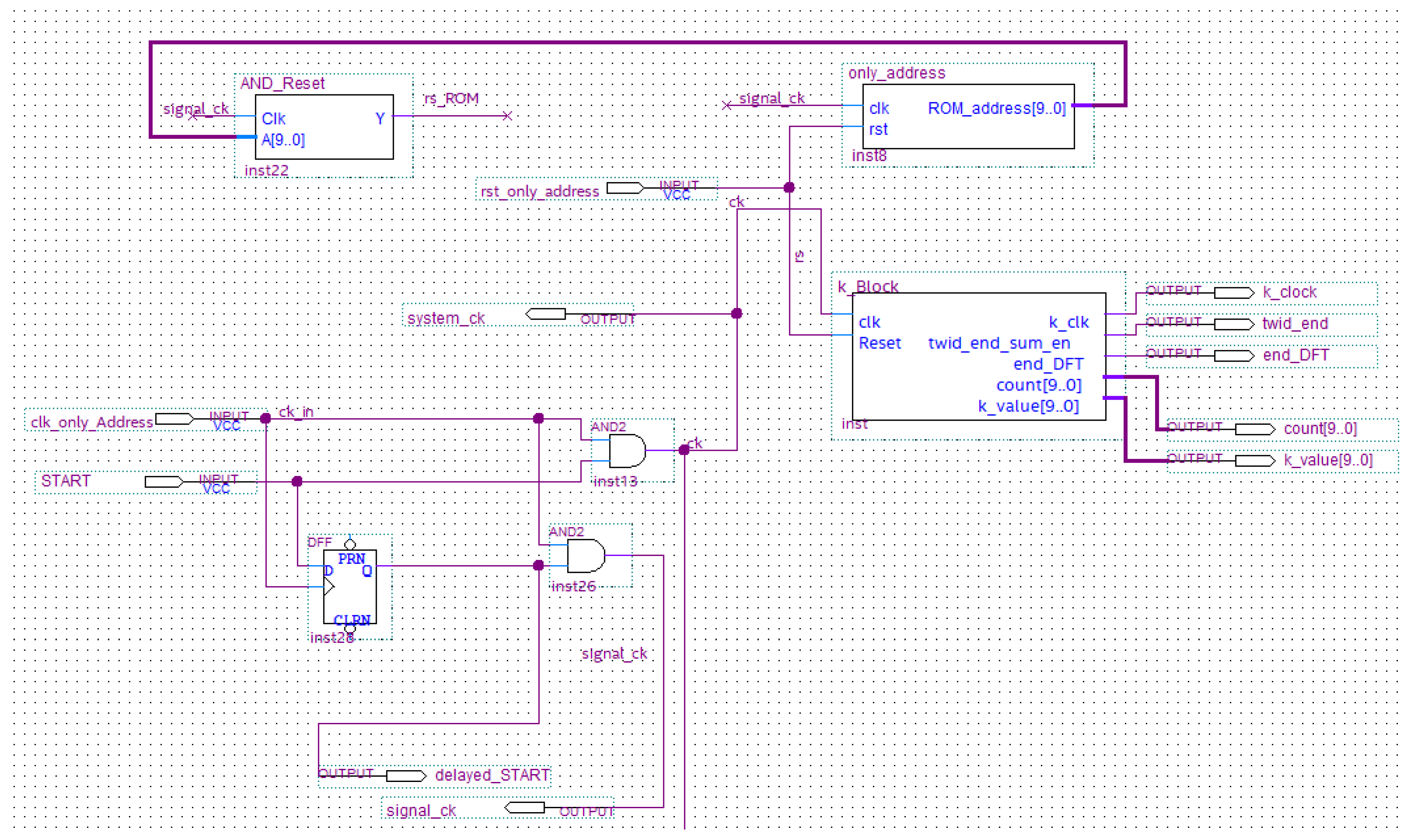
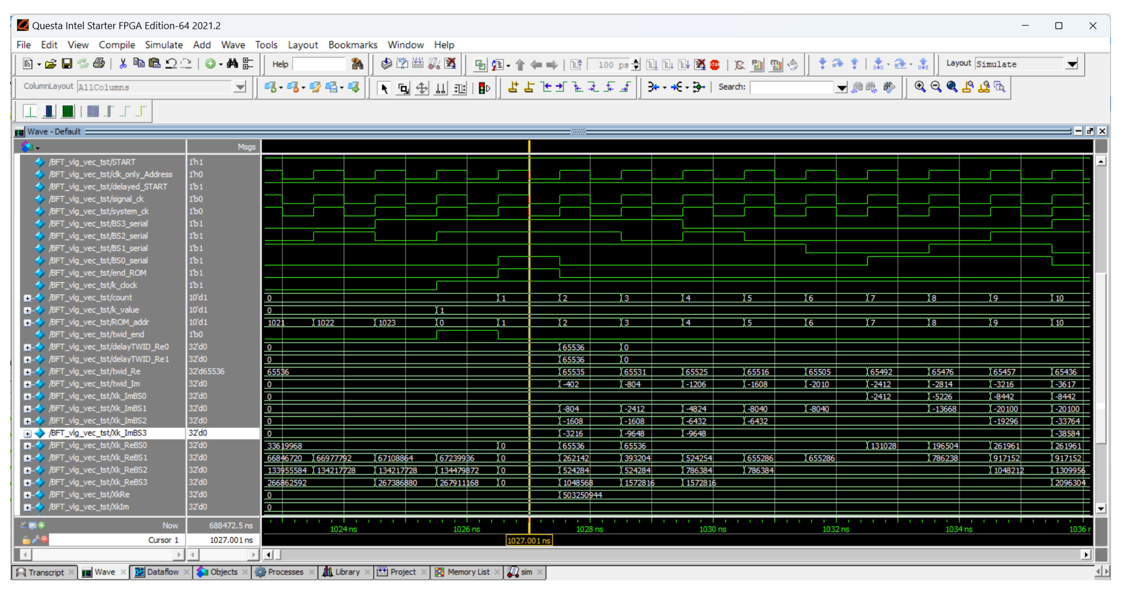
5.2.1. The Timing Block

This module generates all the timing signals, which regulate/control the system operation (Figure 7).
The three inputs of the timing module, named clock, start, and reset, are the timing signal for the system provided by an oscillator/phase locked loop (PLL), a binary signal, which controls the processing starting and the signal for the reset, respectively. The nine outputs are
  • clk, which is the system clock, looked at the START signal. In fact clk is equal to 0 if START is 0 whatever the clock logic value;
  • ROM_address, which is a 10-bit word. It addresses all the signal_ROM memory locations in which a function with 1024 samples is stored. Each sample is coded with 4 bits;
  • END_ROM, which is a binary signal that takes a logic value of one after all the 1024 samples of the signal_ROM have been analyzed;
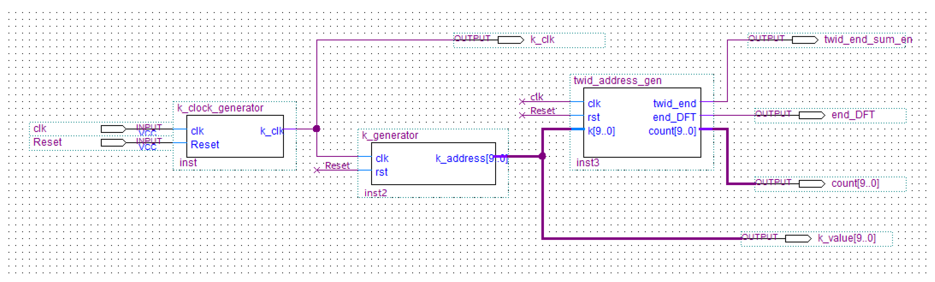
  • K_clock, which is a timing signal for the sum block;
  • K_value, which is a 10-bit word whose numerical value in decimal code indicates the current value of the k index in the expression for the BFT calculation;
  • Count (twiddle address), which is a 10-bit word able to address the twiddle coefficients for their reading.
  • Twid_end, which is a binary signal that reaches the logic 1 value once all the 1024 twiddle coefficients have been sent to the processing block. Selection of 1024 twiddle coefficients is necessary for each processing cycle.
  • Sum_enable, which is a timing signal that controls the operation of adders in the processing block and the correct transmission of both test function samples and twiddle coefficients.
  • End_DFT, which is a binary signal that takes the logic value 1 once all the processing cycles have ended and the BFT values are outputs.
The timing block consists of the below modules/circuits which perform the following functions (Figure 8).
-
AND gate for the implementation of the clock gating technique. The system clock (named ck) is obtained as output only when the START input is equal to 1;
-
only_Address (whose inputs are the system clock and the system reset) is a counter which generates the addresses of the ROM that stores the test signal. For each clock pulse, a 4-bit signal sample is available at the output. This module has been designed in-house by Authors adopting the Verilog hardware description language.
-
AND_reset which is a timed AND gate whose inputs are the system clock and the ROM addresses. The output (named end_ROM) achieves the logic 1 value once all the ROM addresses have been generated that is once all the 1024 samples of the stored function are sent to next stages for processing. Furthermore, this module is designed in-house by Authors in Verilog.
-
k_block which generates ROM addresses (in which twiddle coefficients are stored), a signal for sum block enable and an acknowledge signal to indicate the end of the DFT calculation.
The schematic of the k_block is indicated in Figure 9.
The index to extract the twiddle factor to be used at the generic step can be computed as the reminder of the integer division of the product k · n by N:
i n d e x = m o d ( k · n , N )
This feature can be implemented using a circular register. In our implementation, instead, the proper selection of twiddle factors has been implemented by a m o d N counter that computes the indexes with step k and goes on until the N values needed in the calculation are reached:
T w i d V e c = [ 1 , W N , W N 2 , . . . , W N N 1 ]
Specifically, the k_block updates the twiddle factor for the ( k n ˙ ) -th step of the computation by readdressing: the twiddle factor for a generic k · n value is extracted from the vector defined in Equation (10) selecting the index placed k steps ahead the current position, at each change of the n value.
The modules k_clock_generator and k_generator in Figure 9 have the aim to produce a clock pulse (named k_clock) every 1024 pulses of the system clock and to update the numerical value of the k index every k _ clock, respectively. The module twid_address_gen produces the sequence of ROM addresses in which twiddle factors are stored for each k index value.

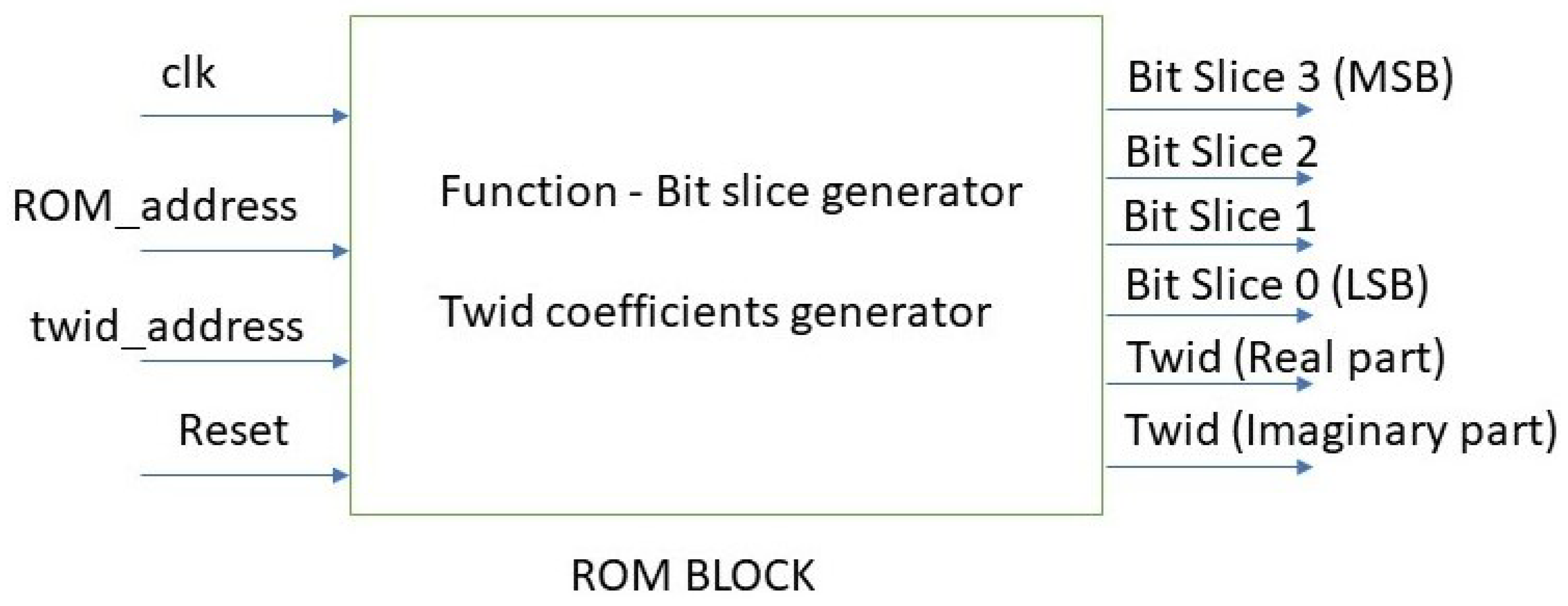
5.2.2. The ROM Block

The ROM block is composed of three ROM memories and its symbol is indicated in Figure 10 with input and output signals. In particular,
  • clk, which is the system gated clock;
  • ROM_address, which are ROM addresses of the signal to be processed
  • twid_address, which are ROM addresses of twiddle coefficients
  • reset
  • Bit Slice 3/2/1/0 are the four bits with which each signal sample is encoded
  • Twid (Real part) and Twid (img part), which are the 32 bits composing the real and imaginary parts of each twiddle coefficient

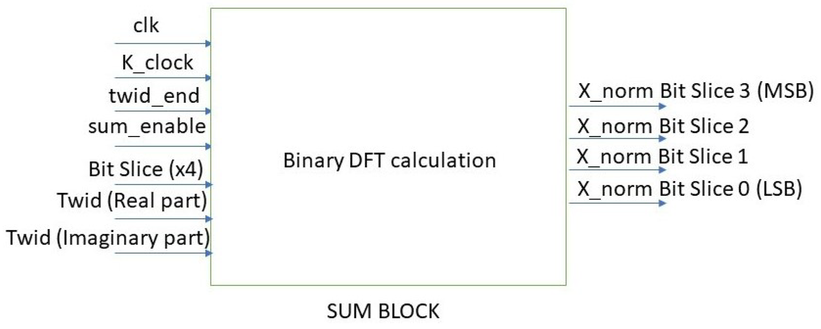
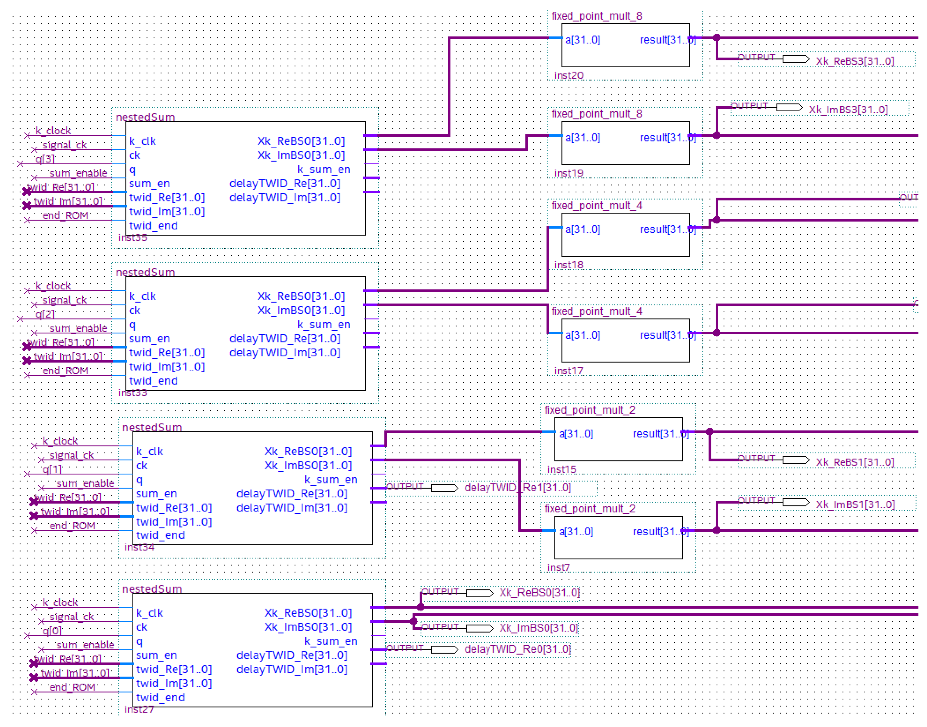
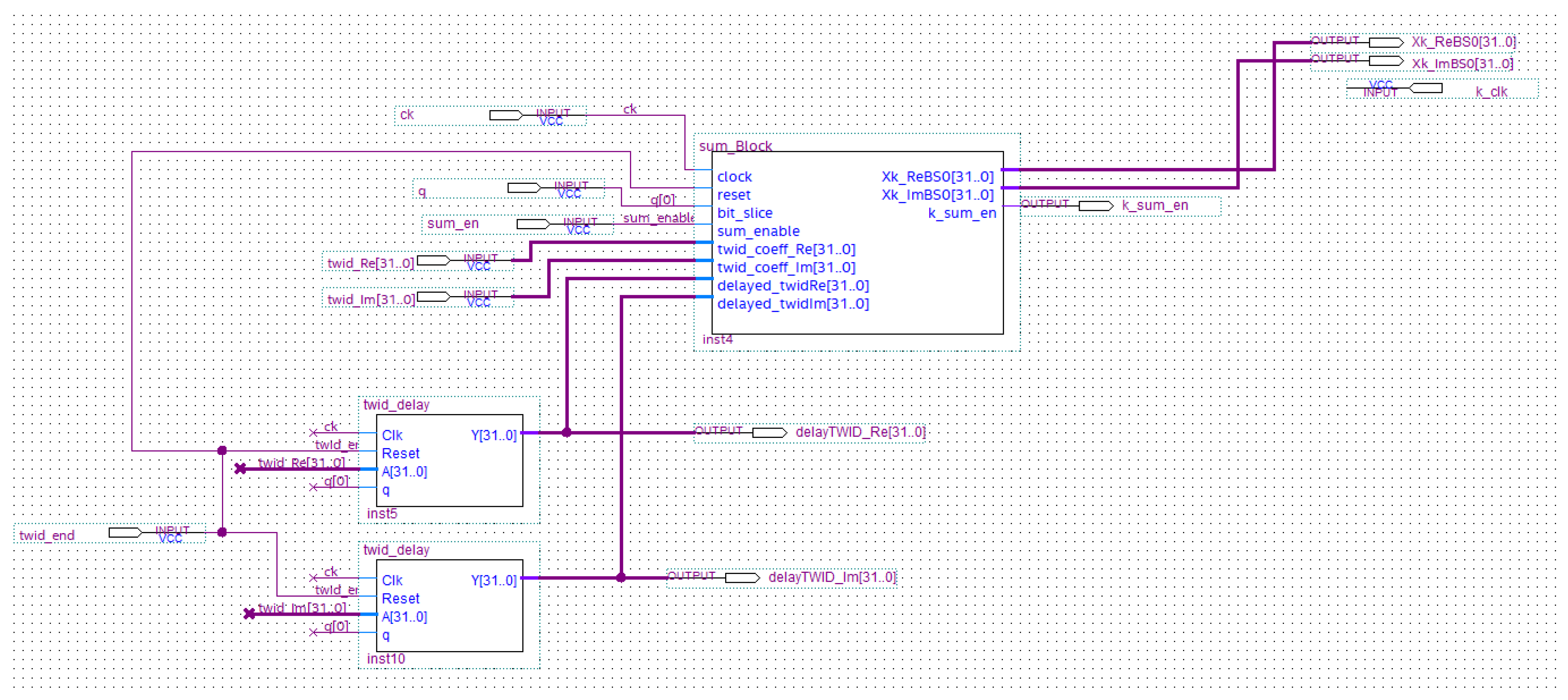
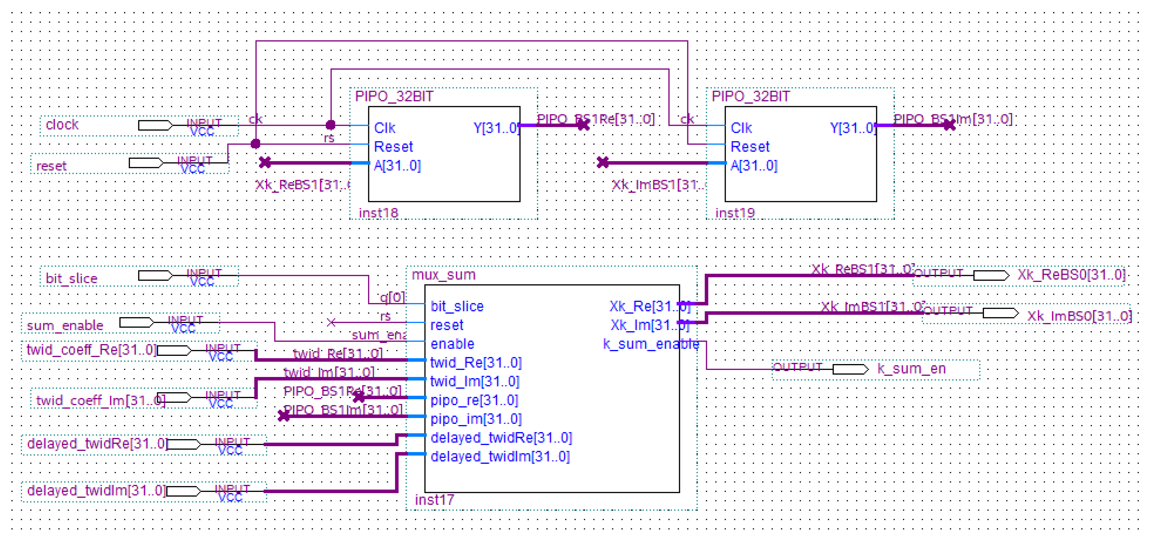
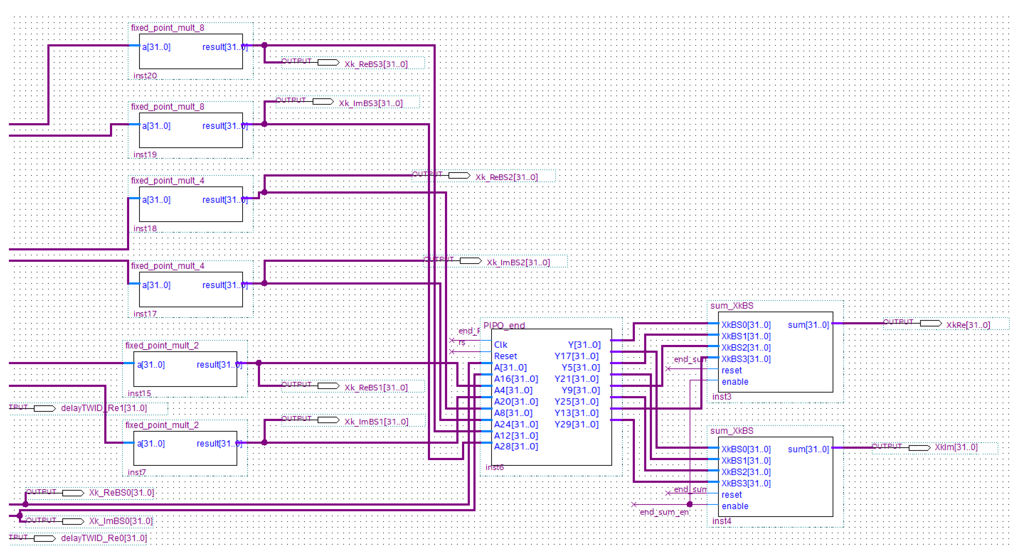
5.2.3. The Sum and Multiplier Block

This block performs the BFT calculation. It can be divided into the adder and the multiplier unities.
THE ADDER MODULE
This processing module makes the BFT calculation according to expressions of Section 3. Figure 11 and Figure 12 show the adder symbol and the schematic in Quartus environment for the selected application example.
The nestedSum unit consists of the below circuits, which perform the following functions (Figure 13):
-
Sum_Block, which evaluates X k for every k value that is generated in the timing block. It is made of two PIPO registers and an adder (mux_sum ) which performs the BFT calculation from Equation (8) in an optimized manner without multiplications as outlined in Section 3 (Figure 14);
-
Two 32-bit PIPO registers, which store the calculated current X k value for one clock pulse;
-
twid_delay, which introduces a suitable delay for the correct twiddle coefficient management by the sum_Block, after the reset signal is generated as a result of the end of the calculation cycle for every k value.
-
end_sumBlock, which adds all the X k values (for k = 0 , . . . , 1023 ) as soon as the sum_block calculates them. It is composed of PIPO registers and an adder (named k_sum) which is designed in-house by Authors adopting the Verilog hardware description language (Figure 15);
Figure 11. Black box representing the SUM BLOCK with the relevant input and output signals.
Jlpea 13 00045 g011
Figure 12. SUM BLOCK schematic.
Jlpea 13 00045 g012
Figure 13. Schematic design of the nestedSum.
Jlpea 13 00045 g013
Figure 14. Sum_Block schematic.
Jlpea 13 00045 g014
THE MULTIPLIER MODULE
These circuits make the multiplication of the DFT of each bit slice using a proper power of two according to expression (7) (Figure 16). For this reason shift registers are used.
Figure 15. Schematic design of end_sumBlock.
Jlpea 13 00045 g015
Figure 16. Black box of the multiplier module with input and output signals.
Jlpea 13 00045 g016

6. Implementation of the FPGA-Based Embedded System

The FPGA CYCLONE IV EP4CE115F29C7 by INTEL was adopted for system development [29]. The design has been deployed on a DE2-115 development board by TERASIC for test and debug purposes [30]. The design environment is Quartus Prime by Intel/Altera [31], but it is portable on any FPGA foundry and development environment.

Efficiency of HW Design

For the designed FPGA-based system, the HW efficiency has been quantified in terms of
  • area occupancy and or amount of used hardware resources;
  • latency, here defined as the time between the reception of the last sample at the input and the availability of the FFT at the output;
  • power consumption due to the system processing activity;
The implemented system not involving the use digital-signal-processor (DSP) devices and occupies less than 1% of the FPGA ALMs resources of the selected chip. Therefore, good efficiency in terms of area consumption is achieved.
Real-time performance is obtained. In fact a latency equal to 1 clock pulse characterizes the implemented system. The yellow line in Figure 17 highlights that all the processing phases start synchronized with a latency of 2 clock pulses.
For power consumption and thermal power dissipation statistic evaluation, the Power Analyser tool operating in post-fitting mode is adopted. This tool is powered by INTEL in the Quartus environment. Adopting a power supply of 5 V, a total thermal power dissipation equal to 307.27 mW is evaluated, in particular it results in 99.06 mW and 208.21 mW of core static thermal dissipation and I/O thermal power dissipation, respectively.

7. Experimental Evaluation and Results

Several experimental evaluations have been performed to verify the proper operation of the designed circuit.
For accuracy evaluation, Matlab calculation result of double precision fixed point FFT number is used as the reference value as a comparison term.
In this study, the data type used to code twiddle factors is a 17-bit fixed-point number, including one sign bit, one integer bit, and fifteen decimal bits (as twiddle factors are complex number with unitary modulus, all the sixteen bits have been used to code them).
Furthermore, to allow proper description of the computed X k output values, a 32-bit word length is used, so that the 1024 sums needed to compute each BFT and the 4 subsequent sums for the composition of the BFT into the transformed coefficients allow to obtain output values without incurring in overflows.
A 32-bit fixed-point number has the advantages of high data accuracy, simpler circuital design and shorter processing delays with respect to a single-precision floating point number [14]. As the representation range of a fixed-point number is limited, the overflow condition that may occur during additions is avoided with the proper choice number of bits of the output word.
The word length increases during output computation. In common fixed point implementations truncations are necessary at the end of sums to restore the selected word length. In our implementation, instead, these truncations are avoided by the proper choice of the processing word length, so that no quantization noise is added above the limit introduced in the twiddle factors coding. The computed DFT accuracy is not affected by this truncation approximation, so that full precision word length is obtained.
For signal-to-quantization noise-ratio (SQNR) evaluation, a sine wave with a relative frequency of 0.2 is considered. The following expression is used:
S Q N R = k = 0 N 1 X k 2 k = 0 N 1 ( X k m X k ) 2
where X k is the FFT evaluated by the proposed system, and X k m is the FFT obtained with Matlab, which implements a floating-point arithmetic with 64-bit precision.
It is well known that expected results may be affected by an SQNR of 6 dB/bit. As our implementation uses twiddle factors coded with 16-bit fixed-point numbers instead, Matlab adopts 52 bits for mantissa representation, and a difference of 36 bits is evaluated for each sample. It follows that the smallest number that can be represented in HW is 2 16 for our implementation so that any SQNR above 96 dB can be considered satisfying.
Pleasing results have been reached with our FPGA system in calculating the BFT. A value of 109 dB of SQNR is achieved for the BFT of a real-sampled sinusoid coded with 4 bits. This result is obtained as no approximation in the computation is performed until the complete computation of the BFT is obtained.
Several other simulations with single sinusoids of different frequencies and coded with the same number of bits have been carried out, obtaining the same performance.
To complete the discussion, a four-bit encoded real low-pass sequence with a 0.2 relative bandwidth has also been tested. In this case, the obtained SQNR is 120 dB.
To verify that there is no intrinsic limitation in the precision of the proposed approach using different word lengths, several computer simulations have been carried out to compare the Matlab implementation of FFT and the proposed approach. Input sequences have been simulated by a real low-pass random sequence, quantized with a variable number of bits between 1 and 52. Figure 18 shows the comparison between Matlab FFT and the proposed method in terms of spectra and absolute difference between spectra at a level of about −270 dB which represents the Matlab precision level. The input sequence in Figure 18 is a low pass signal quantized with 16 bits. Achieved performance is independent of the number of adopted bits for the input sequence quantization that has been tested for values ranging from 1 to 52.

8. Discussions and Conclusions

Hardware solutions of DFT approaches are useful for real-time and high-speed processing applications. Theoretical concepts equal to DFT software procedures are the basis of HW designs, but implementations differ in the approach.
SW procedures are described using standard programming languages and generally have a serial organization fashion. Instead, HW implementations of DFT are usually conceived to develop operating tasks with some degree of parallelism and by adopting a pipeline methodology.
In this paper, a novel, dedicated implementation of the DFT calculation chain is proposed. Input sequence samples are split into bit slices, and each bit slice is Fourier transformed, independently. A simplification in the computational complexity is achieved because only complex sums are required instead of complex multiplies. The method was first developed in the Matlab® environment for debugging purpose, and then the hardware implementation was validated on an FPGA device.
The authors designed the conceived system using an algorithm-to-hardware compiler tool chain and characterized the hardware using the DE2-115 development board by Terasic.
The main contributions of our paper are:
  • Processes on different DFT slices can be carried out in parallel by different circuits with equal hardware structure;
  • The implemented architecture is free of multipliers, and the DFT composition of BFT slices can be accomplished by left-bit shifts of the obtained results;
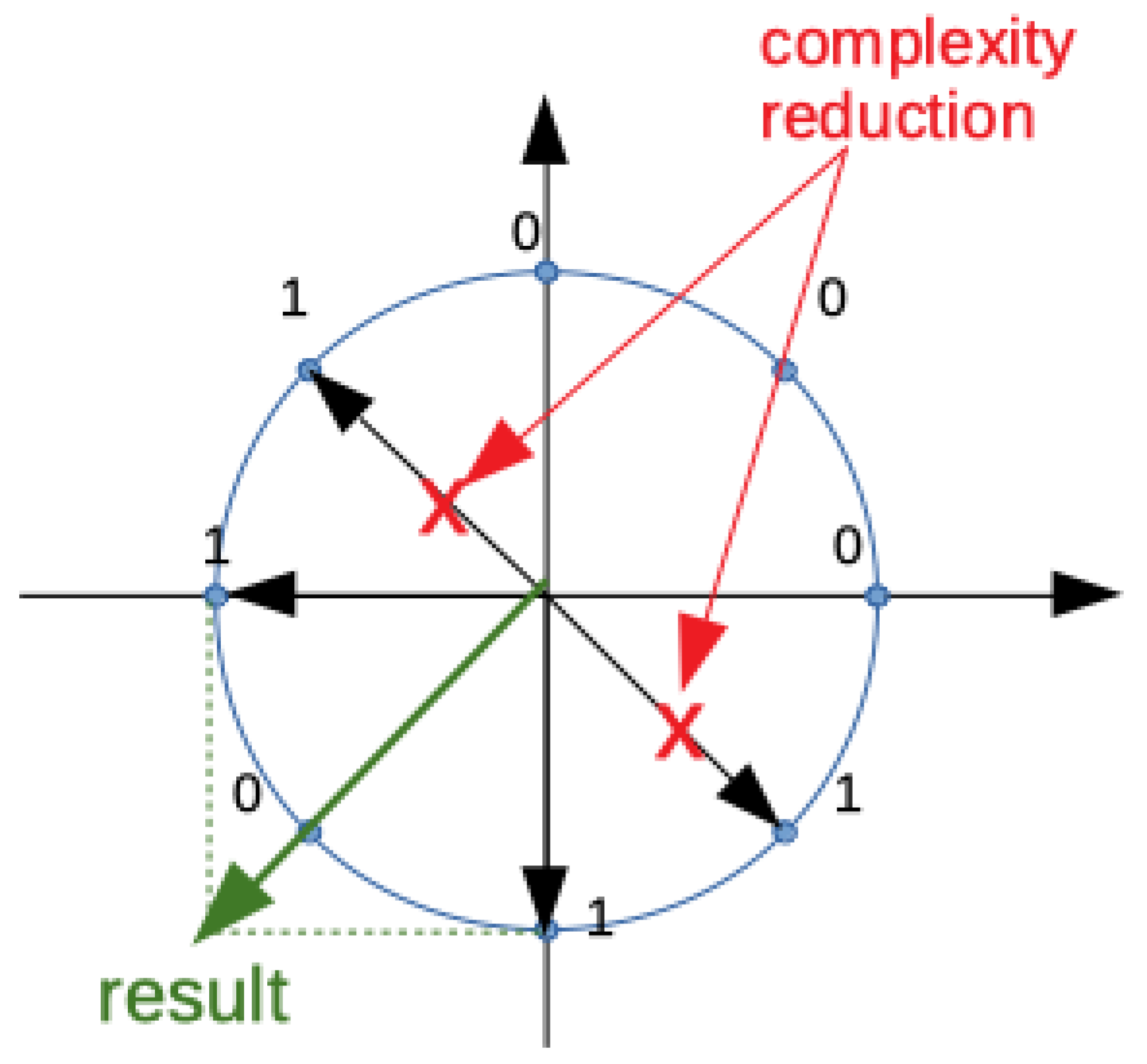
  • The DFT of each bit slice introduces some approximations due to the twiddle factor precision: stated L, the number of bits used to describe twiddle factors, and b, the number of bits of the input sequence. The output Fourier-transformed coefficient can be described, at most, by L + N + b 1 bits, with N being the number of sample points and, consequently, the number of sums needed to compute the BFT coefficient; the b bits are more used to sum the bit slices after proper power of two shifts to compute the X k Fourier coefficients.
  • Full precision can be accomplished in the DFT computation if no approximation is carried out at each computation step. The number of bits describing the DFT coefficients can be L + N + b 1 , after the recomposition of BFT slices into the DFT. In this case, the final approximation in DFT computation is limited by the number of bits used to describe the twiddle factors and a possible final truncation of the output coefficients;
  • A simplification step can be implemented in each DFT slice due to the symmetry inherently present on twiddle factors;
  • The algorithm needs N complex sums for the final DFT composition from BFTs and b · N 2 complex sums for the computation of all the b BFT slices in the worst case (that is when no complexity-reduction step is carried out). If bits are assumed equal in probability of occurrence, N · ( b N + 1 ) / 2 sums are necessary to obtain the DFT because only terms corresponding to ones are summed up. This value may decrease if complexity reduction occurs;
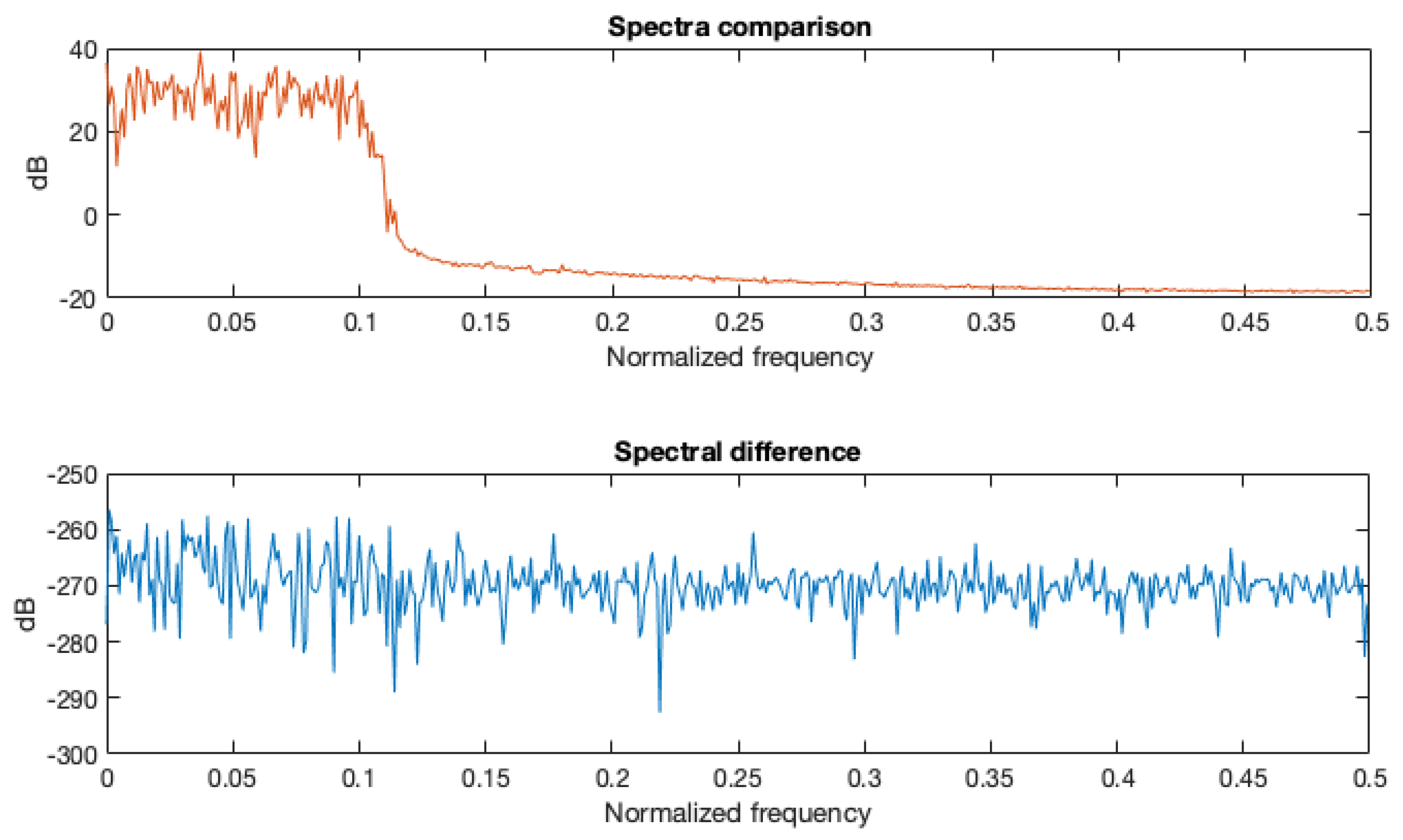
  • A high-accuracy solution was designed. A SQNR above 109 dB is obtained, if compared with the MATLAB double-precision floating-point calculations for a pure sinusoid, and above 120 dB for a low-pass signal.
  • A very low latency implementation of the 1024 points DFT calculation: a two-clock step value is obtained with a clock of 1 n s .
  • The proposed architecture occupies only a small percentage of the total area of the Cyclone IV FPGA (about 1%). It follows that a higher parallelism could be implemented by replicating processing blocks to reduce the latency.

Author Contributions

Conceptualization, C.G.; methodology, C.G.; software, A.G.; validation, A.G., M.R. and C.G.; formal analysis, C.G., M.R. and A.G.; investigation, M.R.; data curation, M.R.; writing—original draft preparation, C.G.; writing—review and editing, M.R.; supervision, C.G. and M.R.; funding acquisition, C.G. All authors have read and agreed to the published version of the manuscript.

Funding

Italian National Recovery and Resilience Plan (NRRP) of NextGenerationEU, partnership on “Telecommunications of the Future”: PE00000001—program “RESTART”, CUP: D93C22000910001.

Data Availability Statement

Not applicable.

Conflicts of Interest

The authors declare no conflict of interest.

References

  1. Kumar, G.G.; Sahoo, S.K.; Meher, P.K. 50 Years of FFT Algorithms and Applications. Circuits Syst. Signal Process 2019, 38, 5665–5698. [Google Scholar] [CrossRef]
  2. Manikandan, P.; Shrimathi, K.; Kiruthika, M.; Mubeena, A. Speech Recognition using Fast Fourier Transform Algorithm. Int. J. Eng. Res. Technol. (IJERT) ETEDM 2022, 10, 29–33. [Google Scholar]
  3. Desai, A.; Gupta, A.; Jambhale, M.S.; Chavan, V. Efficient Implementation Technique for OFDM on FPGA. In Proceedings of the fourth International Conference on Advances in Science & Technology (ICAST2021), Mumbai, India, 7 May 2021. [Google Scholar] [CrossRef]
  4. Cortes, A.; Velez, I.; Turrillas, M.; Sevilano, F. Fast Fourier Transform Processors: Implementing FFT and IFFT Cores for OFDM Communication Systems. In Fourier Transform—Signal Processing; InTech: Rijeka, Croatia, 2012. [Google Scholar] [CrossRef]
  5. Rizzi, M.; Guaragnella, C. A Decision Support System for Melanoma Diagnosis from Dermoscopic Images. Appl. Sci. 2022, 12, 7007. [Google Scholar] [CrossRef]
  6. Giorgio, A.; Guaragnella, C.; Rizzi, M. An Effective CAD System for Heart Sound Abnormality Detection. Circuits Syst. Signal Process 2022, 41, 2845–2870. [Google Scholar] [CrossRef]
  7. Sinchana, G.S.; Padaki, S.; Ravi, V.; Varshini, V.S.; Raghavendra, C.G. Software Implementation of FFT Algorithms and Analysis of their Computational Complexity. In Proceedings of the 2018 International Conference on Electrical, Electronics, Communication, Computer, and Optimization Techniques (ICEECCOT), Msyuru, India, 14–15 December 2018; IEEE: Toulouse, France, 2018; pp. 486–490. [Google Scholar] [CrossRef]
  8. Garrido, M. A Survey on Pipelined FFT Hardware Architectures. J. Signal Process. Syst. 2022, 94, 1345–1364. [Google Scholar] [CrossRef]
  9. Pattan, A.B.; Latha, M.M. Fast Fourier Transform Architectures: A Survey and State of the Art. Int. J. Electron. Commun. Technol. 2014, 5, 94–98. [Google Scholar]
  10. Joshi, S.M. FFT Architectures: A Review. Int. J. Comput. Appl. 2015, 116, 33–36. [Google Scholar]
  11. Xia, K.F.; Wu, B.; Xiong, T.; Ye, T.C. A Memory-Based FFT Processor Design with Generalized Efficient Conflict-Free Address Schemes. IEEE Trans. Very Large Scale Integr. Syst. 2017, 25, 1919–1929. [Google Scholar] [CrossRef]
  12. Giorgio, A.; Guaragnella, C.; Rizzi, M. FPGA-Based Decision Support System for ECG Analysis. J. Low Power Electron. Appl. 2023, 13, 6. [Google Scholar] [CrossRef]
  13. Elango, K.; Muniandi, K. Hardware Implementation of FFT/IFFT Algorithms Incorporating Efficient Computational Elements. J. Electr. Eng. Technol. 2019, 14, 1717–1721. [Google Scholar] [CrossRef]
  14. Li, Y.; Chen, H.; Xie, Y. An FPGA-Based Four-Channel 128k-Point FFT Processor Suitable for Spaceborne SAR. Electronics 2021, 10, 816. [Google Scholar] [CrossRef]
  15. Nash, J.G. Distributed-Memory-Based FFT Architecture and FPGA Implementations. Electronics 2018, 7, 116. [Google Scholar] [CrossRef] [Green Version]
  16. Pereira, P.T.L.; da Costa, P.U.L.; Ferreira, G.d.C.; de Abreu, B.A.; Paim, G.; Costa, E.A.C.d.; Bampi, S. Energy-Quality Scalable Design Space Exploration of Approximate FFT Hardware Architectures. IEEE Trans. Circuits Syst. Regul. Pap. 2022, 69, 4524–4534. [Google Scholar] [CrossRef]
  17. Nori, S.M.; Dawwd, S.A. Reduced area and low power implementation of FFT/IFFT processor. Iraqi J. Electr. Electron. Eng. 2018, 14, 108–119. [Google Scholar]
  18. Elango, K.; Muniandi, K. VLSI implementation of an area and energy efficient FFT/IFFT core for MIMO-OFDM applications. Ann. Telecommun. 2019, 17, 1–3. [Google Scholar] [CrossRef]
  19. Sanjeet, S.; Sahoo, B.D.; Parhi, K.K. Comparison of Real-Valued FFT Architectures for Low-Throughput Applications using FPGA. In Proceedings of the IEEE International Midwest Symposium on Circuits and Systems, Lansing, MI, USA, 9–11 August 2021; IEEE: Toulouse, France, 2021; pp. 112–115. [Google Scholar] [CrossRef]
  20. Godi, P.K.; Krishna, B.T.; Kotipalli, P. Design optimisation of multiplier-free parallel pipelined FFT on field programmable gate array. IET Circuits Devices Syst. 2020, 14, 995–1000. [Google Scholar] [CrossRef]
  21. Ingemarsson, C.; Gustafsson, O. SFF—The Single-Stream FPGA-Optimized Feedforward FFT Hardware Architecture. J. Signal Process. Syst. 2018, 90, 1583–1592. [Google Scholar] [CrossRef] [Green Version]
  22. Hassan, S.L.M.; Sulaiman, N.; Halim, I.S.A. Low Power Pipelined FFT Processor Architecture on FPGA. In Proceedings of the ninth IEEE Control and System Graduate Research Colloquium, Shah Alam, Malaysia, 3–4 August 2018; IEEE: Toulouse, France, 2018; pp. 31–34. [Google Scholar] [CrossRef]
  23. Zhang, X.; Chen, X.; Zhang, Y. Small area high speed configurable FFT processor. In Proceedings of the 2019 International Conference on IC Design and Technology (ICICDT), Suzhou, China, 17–19 June 2019; IEEE: Toulouse, France, 2019; pp. 1–4. [Google Scholar] [CrossRef]
  24. Oshana, R. 4—Overview of Digital Signal Processing Algorithms. In Embedded Technology, DSP Software Development Techniques for Embedded and Real-Time Systems; Newnes: Amsterdam, The Netherlands; Boston, MA, USA, 2006; pp. 59–121. ISBN 9780750677592. [Google Scholar] [CrossRef]
  25. Takahashi, D. Fast Fourier Transform. In Fast Fourier Transform Algorithms for Parallel Computers! High-Performance Computing Series; Springer: Singapore, 2019; Volume 2. [Google Scholar] [CrossRef]
  26. Sindhikar, A.; Mohani, S.P. Review of orthogonal frequency division multiplexing for wireless communication. Int. Res. J. Eng. Technol. 2018, 5, 3609–3612. [Google Scholar]
  27. Roy, S. Advanced Digital System Design: A Practical Guide to Verilog Based FPGA and ASIC Implementation; Ane Books Pvt. Ltd. Publisher: New Delhi, India, 2021; ISBN 978-81-9489-188-8. [Google Scholar]
  28. FPGA Designs with Verilog and SystemVerilog. Available online: https://www.academia.edu/42857396/FPGA$_$designs$_$with$_$Verilog$_$and$_$SystemVerilog?email$_$work$_$card=title (accessed on 1 June 2023).
  29. FPGAs Intel® FPGAs e SoC. Available online: https://www.intel.it/content/www/it/it/products/details/fpga.html (accessed on 1 June 2023).
  30. DE1-SoC Board. Available online: https://www.terasic.com.tw/cgi-bin/page/archive.pl?Language=English\&CategoryNo=165&No=836#contents (accessed on 1 June 2023).
  31. Intel® Quartus® Prime Software. Available online: https://www.intel.it/content/www/it/it/software/programmable/quartusprime/overview.html (accessed on 1 June 2023).
Figure 1. Example of the complexity-reduction step for each 8 point BFT slice.
Jlpea 13 00045 g001
Figure 2. Block diagram of the parallel approach.
Jlpea 13 00045 g002
Figure 5. The 16-QAM OFDM modulation scheme.
Jlpea 13 00045 g005
Figure 6. The block diagram of the proposed architecture.
Jlpea 13 00045 g006
Figure 7. Black box representing the timing block with the relevant input and output signals.
Jlpea 13 00045 g007
Figure 8. Schematic design of the timing block.
Jlpea 13 00045 g008
Figure 9. Schematic design of the k_block.
Jlpea 13 00045 g009
Figure 10. Black box representing the ROM BLOCK with the relevant input and output signals.
Jlpea 13 00045 g010
Figure 17. Timing of processing operations.
Jlpea 13 00045 g017
Figure 18. Spectra comparison between Matlab double precision FFT and the proposed approach.
Jlpea 13 00045 g018
Disclaimer/Publisher’s Note: The statements, opinions and data contained in all publications are solely those of the individual author(s) and contributor(s) and not of MDPI and/or the editor(s). MDPI and/or the editor(s) disclaim responsibility for any injury to people or property resulting from any ideas, methods, instructions or products referred to in the content.

