Abstract
New mission-critical applications, such as autonomous vehicles and life-support systems, set a high bar for the reliability of modern microprocessors that operate in highly challenging conditions. However, while cutting-edge integrated circuit (IC) technologies have intensified microprocessors by providing remarkable reductions in the silicon area and power consumption, they also introduce new reliability challenges through the complex design rules they impose, creating a significant hurdle in the design process. In this paper, we focus on electromigration (EM), which is a crucial factor impacting IC reliability. EM refers to the degradation process of IC metal nets when used for both power supply and interconnecting signals. Typically, EM concerns have been addressed at the backend, circuit, and layout levels, where EM rules are enforced assuming extreme conditions to identify and resolve violations. This study presents new techniques that leverage architectural features to mitigate the effect of EM on the memory hierarchy of modern microprocessors. Architectural approaches can reduce the complexity of solving EM-related violations, and they can also complement and enhance common existing methods. In this study, we present a comprehensive simulation analysis that demonstrates how the proposed solution can significantly extend the lifetime of a microprocessor’s memory hierarchy with minimal overhead in terms of performance, power, and area while relaxing EM design efforts.
1. Introduction
Ensuring chip reliability is a critical design requirement for semiconductor integrated circuits (ICs) to function correctly. To meet this requirement, chip vendors must guarantee a minimum lifetime for each product based on reliability predictions. Design-for-reliability rules have been developed to comply with these requirements. Nevertheless, it has become increasingly difficult to implement these requirements ([1,2,3]) as they rely on processing technology and the IC mission profile, which represents the specific operational conditions and workload. With the continuous emergence of new process nodes and mission-critical applications such as autonomous vehicles, cloud computing, cybersecurity, and medical care systems, the need for high reliability has only been further emphasized.
Electromigration (EM) has become a major factor affecting the reliability of ICs due to the shrinking dimensions of very-large-scale integration (VLSI) circuits, the shrinking density of logical elements into nanometric dimensions, and challenging mission profile conditions. EM primarily impacts the reliability of interconnecting metal wires in ICs. In EM-aware design, three electrical current models are used: the maximum [1], root-mean-square (RMS) currents [2], and average [2,4], which are described in Section 2.
The objective of this study was to examine the impact of the RMS current (RMS-EM) on the memory hierarchy systems of modern microprocessors. The current RMS model relies on the phenomena of Joule heating [5,6], which is induced by an alternating current, resulting in alternating thermal gradients that generate metal fatigue, deformation, voids, and ratcheting metal failures.
Until now, the emphasis in common IS design flows has been on improving the implementation and design flow of ICs [1,2,7,8,9,10,11,12,13] to address EM-related issues, with few studies proposing microarchitectural solutions. In this work, we offer a new microarchitecture that enhances the reliability of the memory hierarchy in modern microprocessors by reducing the impact of RMS-EM and simplifying their design efforts while offering a significant lifetime extension.
Our research is founded on the observation that, in numerous instances, concerns regarding RMS-EM reliability originate from an uneven distribution of write activities, which leads to excessive signal toggling across memory elements. To address this issue, we developed an improved memory resource allocation mechanism that distributed write operations uniformly across all memory elements. Our proposed scheme is similar to two previously introduced solutions for different physical reliability problems. The first one, introduced by Calimera et al. [14] as a solution to a problem relating to SRAM asymmetric aging, suggested reindexing cache lines using various mapping functions. The second method was introduced by Wang et al. [15] to mitigate write endurance in PCM-based nonvolatile memories (NVMs). PCM-based NVMs experience bit-cell wear out after an excessive number of writes, leaving the bit-cell resistance in a low- or high-resistance state. This can happen due to either germanium depletion in the bit-cell area or when the heating electrode is detached [16]. Their proposed technique (similar to Calimera et al.) suggested a swap-shift method to swap a pair of cache sets whenever the number of writes reaches a certain threshold. By using a similar technique, our proposed scheme minimized the occurrence of RMS-EM hotspots caused by individual memory elements, resulting in significantly improved microprocessor reliability. In addition, our solution augments standard electronic-design-automation (EDA) tools, which often assume a worst-case toggling rate due to the absence of the circuit’s architectural behavior and toggle rate, potentially resulting in overdesign and shorter device lifetimes. While the focus of our study is on microprocessors, the ideas and methods presented in this work can be extended and applied to various other integrated circuits and applications. We summarize the contribution of this study as follows:
- We offer solutions that exploit architectural characteristics to reduce the impact of RMS-EM in modern microprocessor memory hierarchy.
- The suggested architectural approach can be combined with standard physical design flows to augment current RMS-EM handling methods.
- The proposed solution incurs a minimal cost in terms of power, performance, and silicon-area overhead, with no compromise on reliability or IC lifetime.
- Our comprehensive experimental simulations incorporate both EM physical and architectural simulations, which collectively validate our suggested architectural solutions at a physical level.
The remaining sections of this paper are organized as follows: in Section 2, we provide the EM background and review prior work. Section 3 explains the current limitations of the memory hierarchy in modern microprocessors when handling EM-related concerns. Then, Section 4 describes our RMS-EM architectural solution for memory hierarchies. In Section 5, we describe the experimental results for both the microarchitectural and physical simulations of the proposed EM-aware microarchitecture. Lastly, Section 6 summarizes our study and outlines future working directions.
2. Prior Works and Related Background
Over the last decade, with the introduction of nanometric advanced processing technologies, susceptibility to reliability-related issues has significantly increased. In particular, EM is considered one of the most challenging reliability concerns in relation to the aging process of IC wires, as it affects both the lifetime and performance of ICs. The semiconductor industry has dedicated significant efforts to overcoming EM reliability challenges by improving physical design implementation flows. However, this approach necessitates significant design efforts and frequently demands multiple iterations to ensure its compliance with design rules. However, there have been few studies that tackle these challenges in relation to reliability by considering architectural aspects. This section presents an overview of EM and summarizes related prior works.
2.1. Electromigration Overview
The physical phenomenon of EM affects wire reliability in ICs, provoking voids and shorts in metal wires and reducing the median time to failure (MTF). Even a single wire failure due to EM can manifest an entire IC failure, making it a significant concern for nanometric processing technologies [11]. To model the MTF of a single interconnect segment, Black’s equation [17] is commonly used:
where J is the density of the current, n is a factor of scaling, Ea represents activation energy, A is a constant, KB is the Boltzmann coefficient, and T is the operating temperature. The exponential relationship between temperature and MTF means that higher temperatures accelerate EM by weakening the bonds of the atoms within a metal wire, resulting in a higher vulnerability to EM forces. This underscores the EM-related challenges faced by mission-critical applications, such as autonomous vehicles, which operate at high temperatures. Foundries enforce special design-rule constraints on all three current models [18] to meet EM reliability requirements.
Applying peak current, even briefly, creates stress from the conduction of metal ions and electrons. If the kinetic force from the electrons becomes strong enough, it may move metal atoms in the course of the electrical current flow, potentially inducing wire damage. EM-induced destruction to a metal interconnect can cause a conductivity drop or the creation of hillocks and voids [1], all of which can potentially manifest in an overall system failure. The EM model of average current involves an oscillating current, which induces material backward flow [2]; this reduces atom migration overall and can mitigate EM-related failures due to the self-healing phenomenon [4]. While the average and peak models are ruled by the kinetic energy of an electrical current, the RMS current model [5,6,18] is induced by a switching current, which induces thermal oscillations. This can induce wire deformation and result in voids, exhaustion, and increases in the probability of failures in metals. The phenomenon referred to as Joule heating or RMS-EM cannot be alleviated through self-healing methods [2]. The propagation of thermal fluctuations caused by RMS-EM can have a spatial impact, leading to the deterioration of neighboring metals. The MTF due to RMS-EM is given by the following equation [18]:
where the frequency is represented by Fmax. The capacitance is represented by C, the metal height and width are represented by W and G, respectively, the operating volta is VDD, the toggle rate (switching probability) is represented by p, and the rise time and fall time are represented by tr and tf, respectively. It should be noted that Joule heating and current-induced electromigration (maximum and average current EM) are interrelated, with one affecting the other. Joule heating raises the temperature and creates temperature gradients, which leads to atomic diffusion and accelerates current-induced EM. Conversely, current-induced EM causes an increase in resistance and the density of the current, which increases the temperature and intensifies Joule heating. The reciprocal positive interaction between Joule heating and current-induced electromigration can lead to a significant acceleration of both phenomena, giving rise to substantial reliability concerns.
Today, foundries enforce a maximum level of the RMS current (IRMS-max) for a specified lifetime, and EDA tools are required to validate the compliance of every net in the IC and fix any related violations. Implementing the design rules for RMS-EM can prove challenging due to their reliance on the switching probability, which is dependent on both the IC architecture and the workload. Write operations, executed by a microprocessor or control modules to alter the logical state of bit-cells and wires, primarily govern the probability of switching in memory elements. While read operations may also trigger wire state changes, these mostly occur on the read ports of memory elements; thus, they play a smaller role in contributing to RMS-EM hotspots. Further work on EM and its reliability impact are available in [1,2,12,13,19,20].
2.2. Prior Work on Electromigration
The physical design aspect of EM has been extensively researched. Numerous studies [7,10,21] have analyzed the impact of EM on various types of interconnect materials in various processes, temperatures, and voltage conditions. The prevailing physical solution is to increase the width of the wires, which, as shown in Equation (2), extends MTF and ultimately mitigates EM effects. However, widening wires from a physical design perspective can lead to additional complications, including an increased die area, which can induce timing violations.
During the IC design flow, EDA tools utilize processing technology EM rules to ensure that wires and vias adhere to EM design specifications. These tools also identify any violations in relation to EM and highlight areas that necessitate design fixes. To simulate switching activity patterns, RMS-EM analysis tools can be utilized, which represent real applications and consider these patterns in the analysis. In situations where determining the worst-case toggle probability is challenging, designers often depend on the statistical simulation offered by EDA tools. However, this approach can sometimes result in overdesign. The process of fixing RMS-EM violations involves numerous iterations and trials due to the complex design rules. Dasgupta et al. [7] developed a methodology for synthesis so that data transfers could be scheduled with an emphasis on EM awareness. Their proposed algorithm necessitates pre-determining the toggle rate, resulting in tight coupling to a specific workload. A comprehensive review of physical design flows to mitigate the effect of EM can be found in [13].
Previous studies have proposed architectural approaches to handling EM; however, the number of such studies is limited. Srinivasan et al. [9] introduced a duplication of hardware structural and graceful performance reduction methods to address the EM effect. The duplication of a hardware structure involves adding spare logical elements and interconnects to the IC, which can be activated when certain elements fail with the graceful performance reduction powers of failing elements and maintaining the IC’s functionality, albeit with degraded performance. Nonetheless, this approach results in a substantial overhead as it necessitates specialized mechanisms for EM degradation during a regular IC operation and specific circuits to activate the redundant logic. Furthermore, it involves additional performance and power overheads because of the redundant hardware. An analogous approach involving the addition of redundant elements to mitigate EM was proposed by [22].
Abella et al. [11] proposed a microarchitectural solution for “refueling” dual-directional buses by tracking the electrical current direction on the bus whenever data were transmitted. Their solution suggested a current compensation mechanism that would alleviate the EM impact caused by the peak current in the event of any imbalance between the currents flowing in each direction. However, this technique could promote RMS-EM resulting in reliability concerns. Additionally, bidirectional buses are not commonly utilized in modern VLSI circuits due to their design complexity. The refueling mechanism interrupts the bus operation and has the potential to increase dynamic power. Srinivasan et al. [8,23] proposed a dynamic approach for managing reliability, in which the processor adjusts its lifetime reliability target based on the application’s changing behavior. By adopting this strategy, it becomes possible for a lower-reliability processor to operate correctly, albeit at the expense of performance or operating conditions. In [24,25], the authors proposed architectural solutions that could leverage the characteristics of the architecture to decrease the RMS-EM impact on the execution units and register file structures in modern microprocessors. Their results indicated that their solution could extend the lifetime by at least 2× for the execution units and 10× for register files.
3. EMS-EM Hotspots in Memory Hierarchy
Our study was motivated by the fact that the switching probability is inversely proportional to MTF, as indicated in Equation (2). Performing RMS-EM analysis based on the switching probability introduced several challenges:
- The switching probability factor depends on both the memory system architecture and the workload, making it difficult to determine its value.
- Current RMS-EM EDA tools cannot differentiate between the toggle rate of different logical elements in the IC, which can lead to overdesign.
Therefore, we aimed to enhance MTF by reducing the switching probability and avoiding hotspots in memory hierarchy systems that could lead to RMS-EM-related failures. This approach will also help mitigate the challenges mentioned above.
In this study, we assumed that all other variables, except the toggle rate in Equation (2), remained unchanged. Although the junction temperature significantly impacts the RMS-EM MTF, its value depends on the cooling solution and computational workload assumptions. As a result, common design flows typically account for the worst-case scenario, considering temperatures of 105 or 125 °C. Additionally, we assumed the IC operation at a standard process node voltage. Finally, the capacitance parameter was dependent on wire geometry: the inherent capacitance of a process node.
In the next subsection, we describe our experimental environment for analyzing the switching probability in the memory hierarchy of modern microprocessors. We also examine the distribution of the switching probability over memory hierarchy elements. It should be noted that the impact of EM on the power grid is not addressed in this paper, and our focus is on signal nets.
3.1. Experimental Environment
We conducted our experimental analysis using the Sniper simulator of an x86-64 microprocessor [26], in which we incorporated the essential mechanisms to simulate the behavior and quantify the necessary characteristics needed for our study. The simulator comprised a comprehensive x86 core model at the cycle level and a memory hierarchy. The simulator was configured to the Intel Gainestown core [27], and Table 1 provides a summary of the configuration. We utilized the Spec2017 benchmark suite [28,29] with ref inputs for our experiments. The benchmark suite encompassed applications from diverse domains, including machine learning, liquid flow simulation, vision processing, and document parsing. SPEC has been the widely accepted benchmark suite for various microprocessor research domains in both the industry and academia. In our experimental analysis, we executed each benchmark workload, with every experiment encompassing 10 billion instructions.

Table 1.
Configuration of the simulation mode model’s configuration.
3.2. RMS-Electromigration Hotspots
In this section, we examine the hotspots of the toggling rate that encouraged RMS-EM in the microprocessor’s memory hierarchy subsystem. We were motivated to investigate memories because they employ dense bit cells featuring elongated and slender metal interconnects that alternate with each change in the logical state, making them highly susceptible to RMS-EM. Static RAM (SRAM) memories use lower metal layers for their interconnect, typically three metal layers, which have significantly smaller geometrical dimensions. As a result, they become highly susceptible to RMS-EM. In addition, physical design tools cannot handle every bit cell individually; therefore, the worst-case toggling rate is commonly applied to all bit cells. As memory writes are not evenly spread across all memory bit cells, the worst-case scenario is established by the bit cell exhibiting the highest rate of switching.
We started our analysis by examining the toggle rate of the memory hierarchy elements. Figure 1 illustrates the ratios of the average count of writes per bit cell across the various elements in the memory hierarchy of microprocessors. It revealed that the Data Translate Lookaside Buffer (DTLB) encompassed a substantially bigger write count than the Instruction Translate Lookaside Buffer (ITLB). The DTLB also entailed approximately ten times as many writes as the Secondary Translate Lookaside Buffer (STLB). A comparable observation arose when analyzing the ratio of write counts between the L1-D cache and the L1-I cache. The latter entailed writes only when the blocks were replaced, whereas the L1-D cache performed writes during the replacement of lines and whenever a store instruction modified a memory location, thus resulting in a significantly higher number of writes. Continuing to compare the write ratios of the remaining memories in the memory hierarchy system showed that higher levels of cache memories experienced a higher toggling rate.
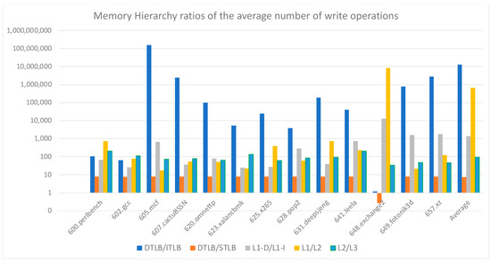
Figure 1.
Write ratios in memory hierarchy.
While our preliminary observations highlight the DTLB and L1-D as having the topmost write rates, we also investigated the write behaviors of both the L2 and L3 caches. Their physical design had a higher susceptibility to RMS-EM than the first-level caches, mainly because they utilized denser bit cells in conjunction with narrower and longer metals.
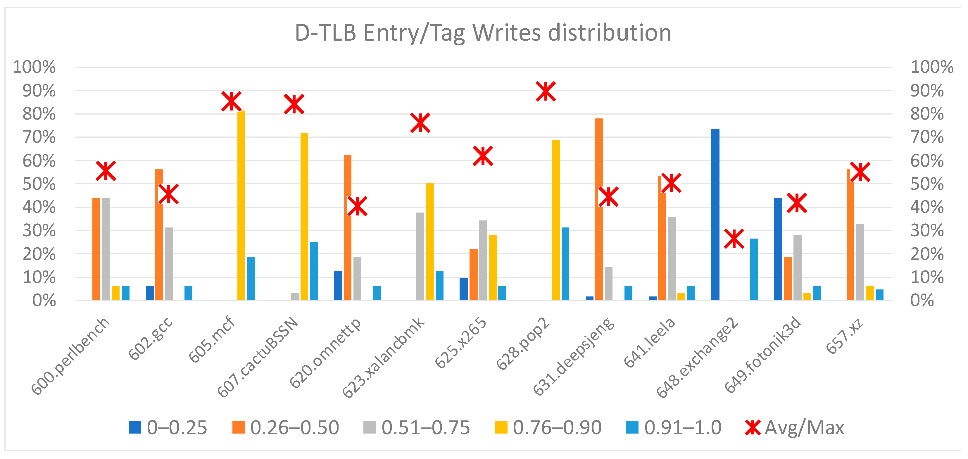
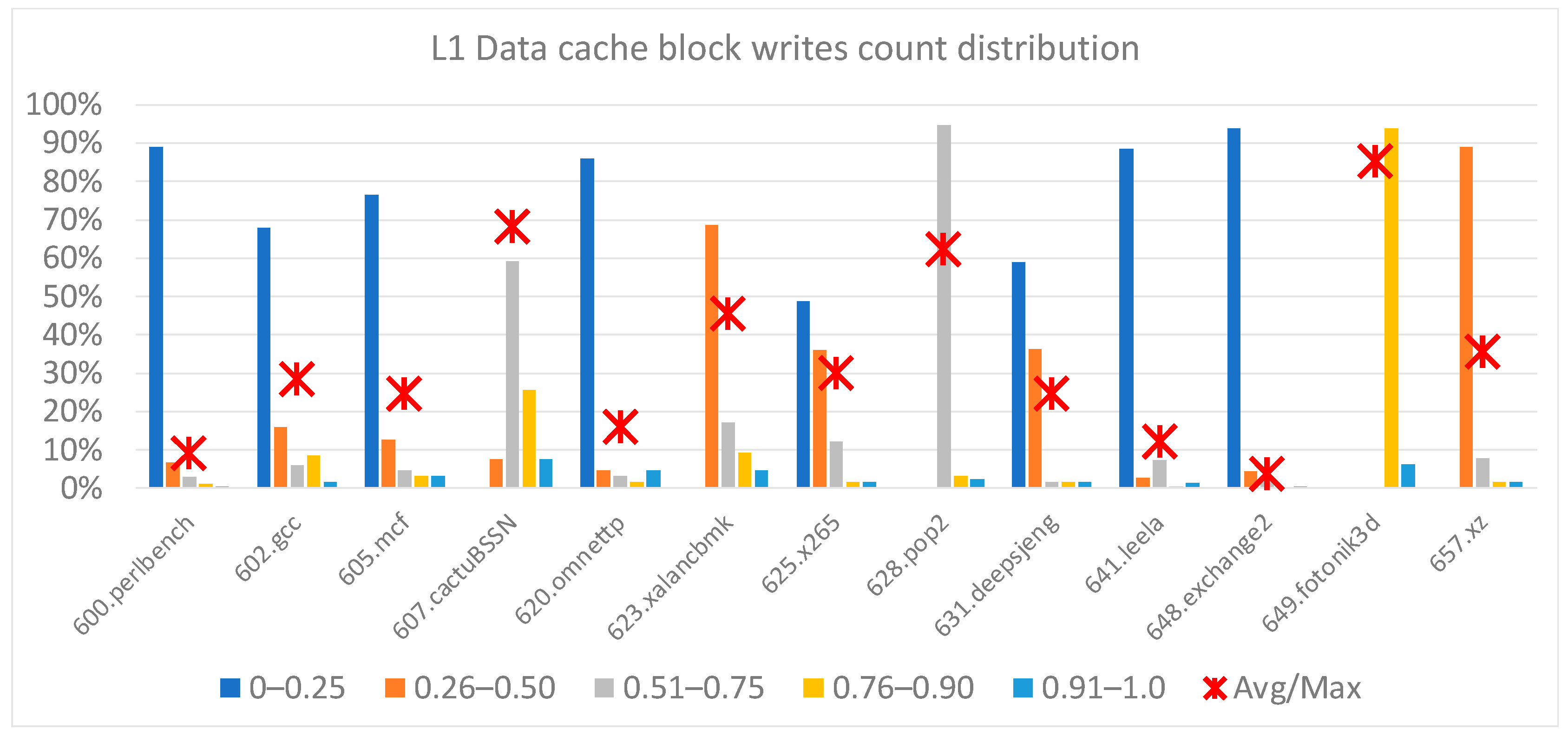
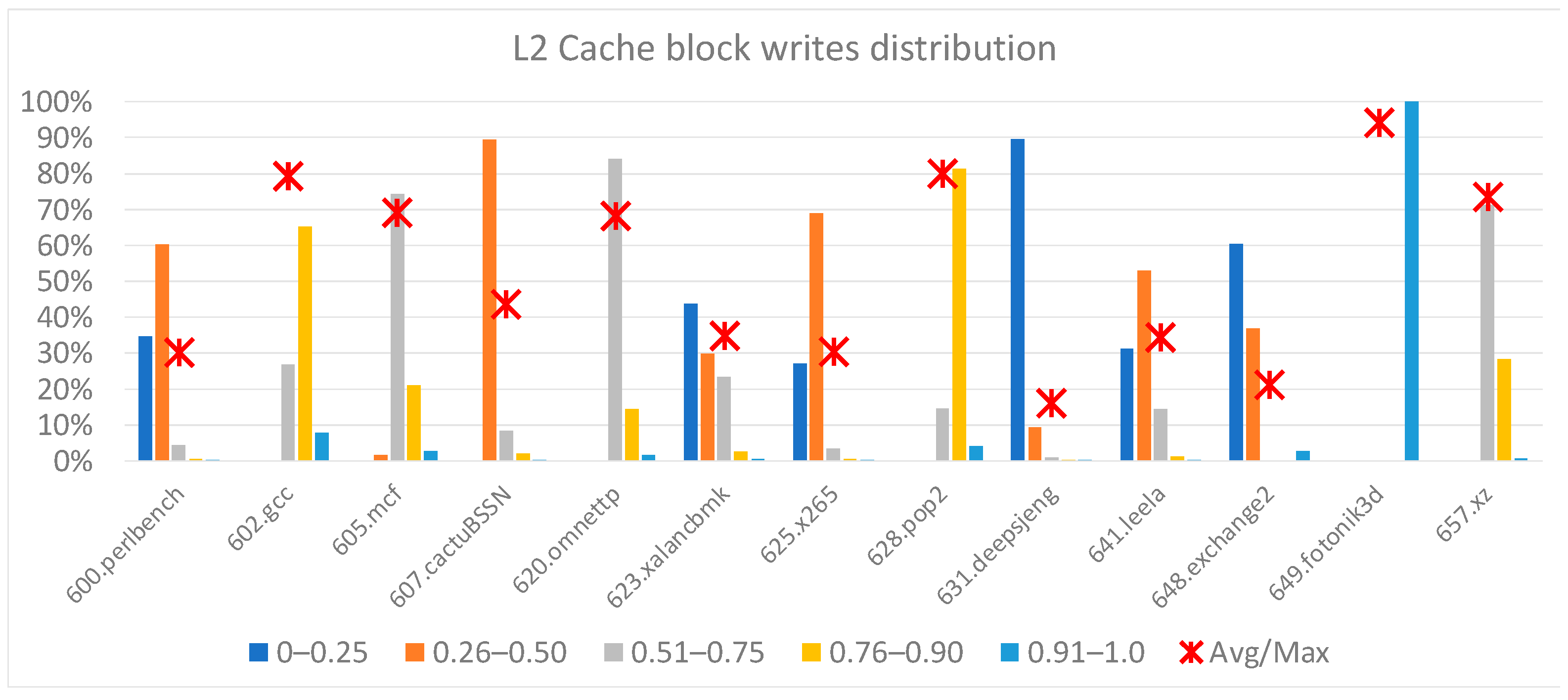
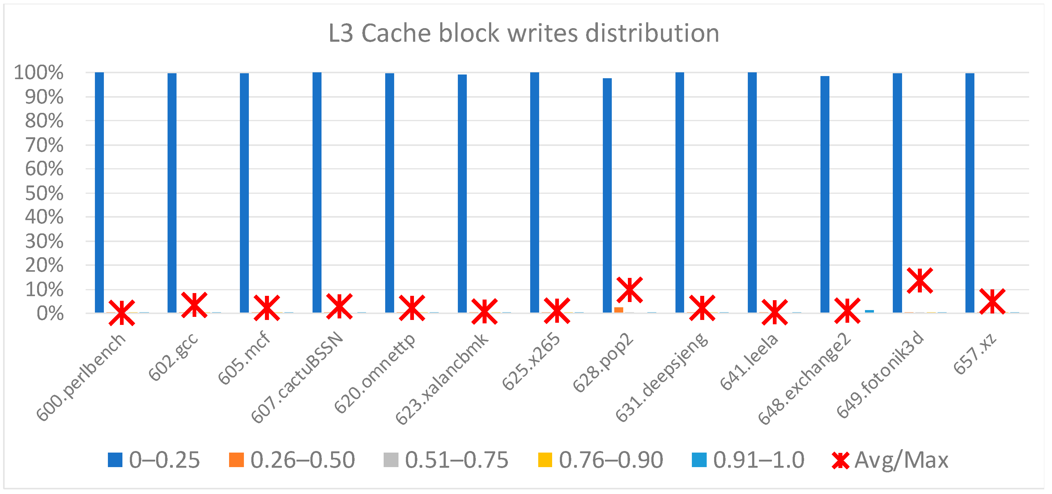
Our next experimental analysis measured the distribution of write operations in the DTLB, L1-D, L2, and L3 caches. Figure 2, Figure 3, Figure 4 and Figure 5 illustrate five-bin histograms: 0–25%, 26–50%, 51–75%, 76–90%, and 91–100%. Every bin in the graph represents the count of cache blocks with the ratio of the write count to the cache entry with a maximum count of writes. E.g., 30% for bin 51–75% indicates that 30% of the blocks had a write count in a ratio range of 26–50% relative to the block with the highest write count. The block with the highest count of writes determined the assumed toggle rate for RMS-EM for the entire cache. Such histograms help illustrate the switching probability spreading among all the blocks and help us study new solutions to relax RMS-EM hotspots.

Figure 2.
Distribution of DTLB writes.

Figure 3.
Distribution of L1-D cache block writes.
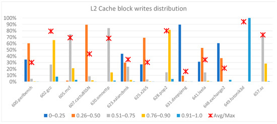
Figure 4.
Distribution of L2 cache block writes.
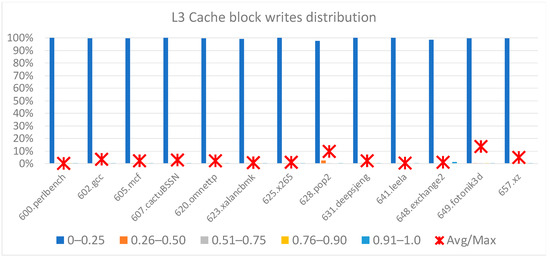
Figure 5.
Distribution of L3 cache block writes.
Figure 2 illustrates the histogram of entries in DTLB. Note that, for all the benchmarks, only a small number of entries experienced a large ratio (above 90% relative to the entry with the maximum number of writes). These entries dictated the overall switching rate of the DTLB. Most entries experienced much lower write rates. Figure 2 also presents the ratio of the average number of writes per entry to the maximum number of writes for all entries, which varied from 2% to 100%, with an average of 55%.
Figure 3 shows a histogram of the writes to L1-D cache data lines. The situation appears similar to that observed in the DTLB. Only a small number of cache lines had a high write ratio (above 90% relative to the maximal data cache line), whereas the majority of cache lines experienced much lower write ratios. In most of the benchmarks, the ratio of the average number to the maximum number of writes was less than 30%, whereas the average ratio was 33%.
In Figure 4, we present a histogram of the writes to the L2 cache data lines, which were similar to those for the L1-D cache. For both data blocks and tags, we observed that only a small portion of cache entries (data and tags) experienced the highest write ratio (>90% relative to the entry with the maximum number of writes), and as a result, they indicated severe RMS-EM conditions for all cache entries. We could observe that the ratio of the average number of writes per entry to the maximum number of writes in all the entries was approximately 50%. A similar result for write operations on cache lines was also obtained by Valero et al. in their study on the different aspects of cache reliability [20]. One may notice in Figure 3 and Figure 4 that the benchmark 649.fotonik3d behaved differently than all the other benchmarks. This was because the 649.fotonik3d write distribution spread uniformly over most cache lines.
Figure 5 shows a histogram of L3 writes for cache data lines. For most benchmarks, the number of writes was for the majority of cache data lines, where almost all of them experienced 25% or fewer write operations relative to a small portion of cache lines with the maximum number of writes. Overall, the ratio of the average number of write operations to the maximum number of writes was 8%.
Our additional experiments, which also included of analysis on the cache tag writes, indicated that tag writes were spread more uniformly than data lines, and the majority of cache tags experienced a smaller variance in the number of writes. The ratio of the average number of tag writes to the maximum number of tag writes was nearly 70% on average for the L1-D cache and approximately 50% for L2 and L3 tags.
The results presented in this section support our observation that cache data lines experience a switching probability distribution with high variance, and a minority of lines were highly stressed by the maximum number of write operations. This, as a result, dictated much more severe RMS-EM conditions for the entire cache. Similar conclusions were obtained from our observations on the register write access and ALU use, where, in both cases, the switching probability induced by the workload was nonuniformly distributed. Such behavior led to an overdesign condition for RMS-EM that could degrade the overall performance and increase the IC area.
4. RMS-EM-Aware Memory Hierarchy
In this section, we present our proposed architecture solution to mitigate switching probability hotspots in the memory hierarchy, which, in turn, relaxes the sign-off conditions required for RMS-EM. The core idea behind our solution was similar to workload balancing techniques used in computer systems. We used a resource allocation scheme that was aware of the switching probability to uniformly distribute the utilization of computational resources. This approach smoothed out the utilization, which significantly reduced the impact of RMS-EM on reliability.
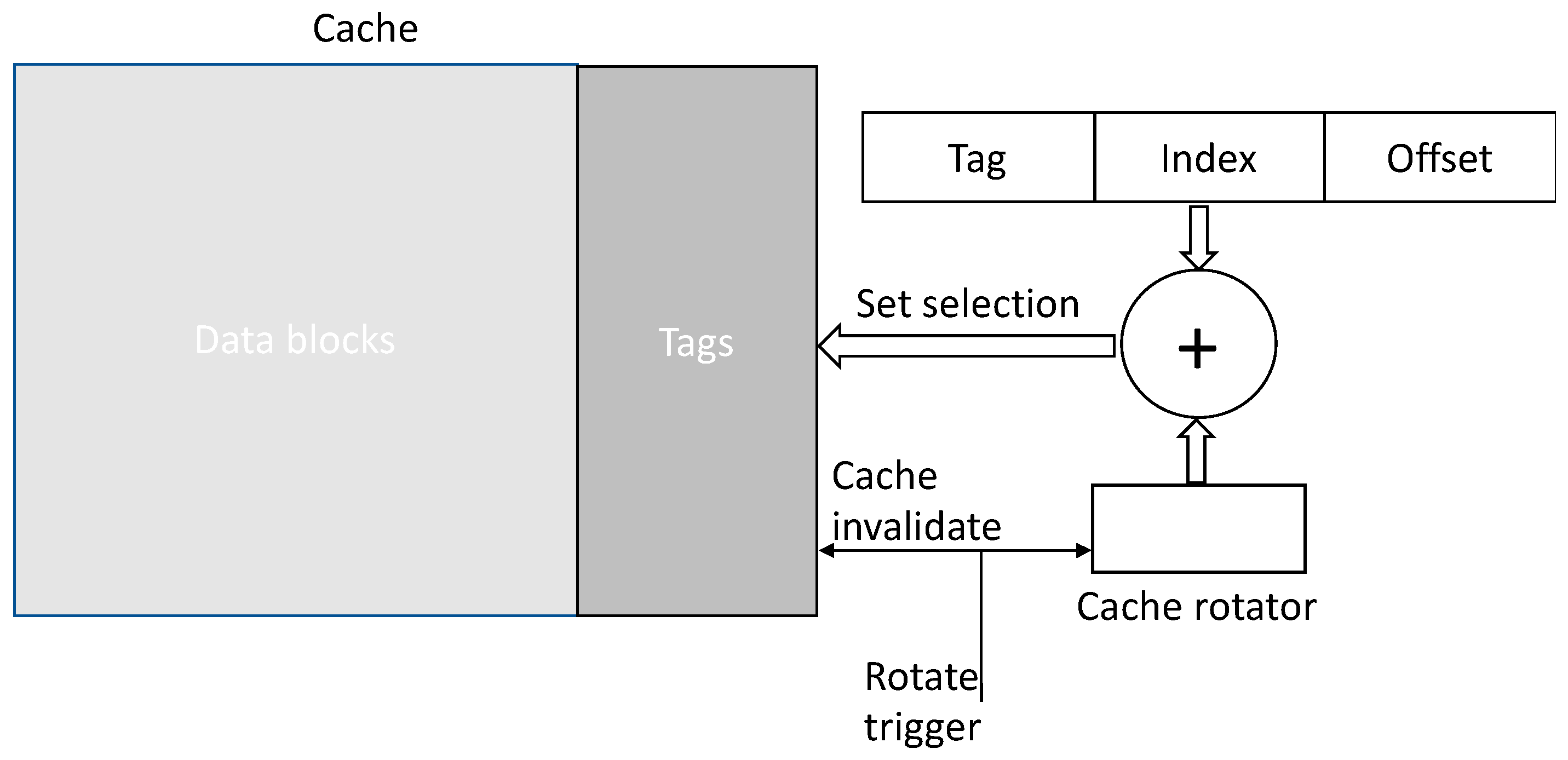
Cache memories could generate RMS-EM hotspots in cache lines that were spread nonuniformly. Note that, in this subsection, the term “cache” refers to any architectural structure that uses a cache organization (e.g., TLBs). As a result, a small fraction of the cache lines could dictate the worst RMS-EM scenario for the entire cache. The principle of the proposed EM-aware cache memory scheme, illustrated in Figure 6, is based on similar principles of the register file solution.
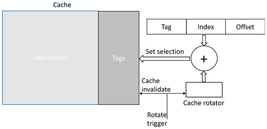
Figure 6.
Electromigration-aware cache memory mapping.
Our proposed scheme avoided hotspots of cache writes by periodically changing the cache set mapping of cache blocks to their corresponding physical cache lines. As with the RF solution, this scheme was based on the modulo rotation of the mapping between the set field (taken from the block address) and its physical set location. Our suggested mapping method calculated the cache set number by adding the block index field to a modulo counter. The counter determined the physical index shifting relative to the cache block’s original index. A periodic pulse trigger was maintained to shift the mapping of the cache sets. After each assertion of the pulse trigger, the modulo counter was incremented, and all cache lines were invalidated. Note that this cache-invalidation circuitry already existed in many modern microprocessors for cache-context invalidation; therefore, the proposed method did not incur an additional overhead by adding this mechanism. In addition, the periodic pulse trigger could operate at a relatively low frequency to ensure negligible performance overhead due to cache invalidation. The result was that this approach avoided write hotspots by periodically spreading the cache line mapping across all the cache sets. Table 2 summarizes the power, critical timing path impact, and area overhead for the 28 nm process of all the logical elements proposed by our technique and are illustrated in Figure 6 for different cache configurations:

Table 2.
Cache rotator overhead.
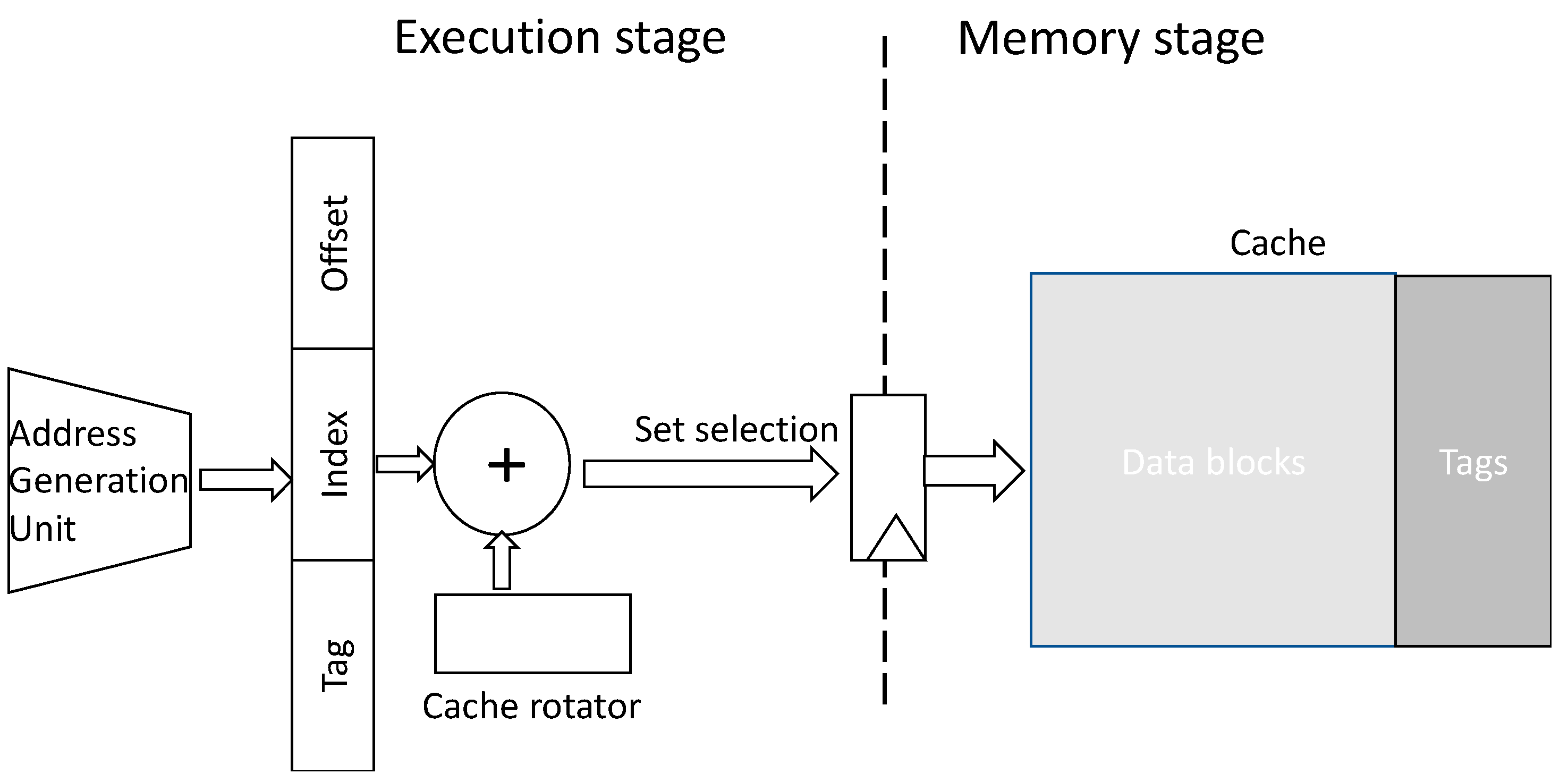
As can be observed in Table 2, the proposed scheme introduced negligible power and the area overhead to the system. In addition, the timing impact of the EM-aware cache mapping fell within the range of 60–76 ps. Assuming a 2.66 GHz clock frequency and considering that the cache access port was on the critical path, this timing impact resulted in a 20% reduction in clock frequency. To mitigate this clock frequency degradation, we suggested retiming the set index calculation to an earlier pipeline stage and thereby removing this calculation from the processor’s critical path. This process of retiming is illustrated in Figure 7, where the set calculation was performed right after the memory address generation performed by the address generation unit (AGU). Our timing analysis on the AGU indicated that it utilizes less than 40% of the clock cycle time of the processor and thereby retiming the set calculation avoided degradation in the clock frequency.
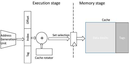
Figure 7.
Retiming of cache memory set selection.
To avoid the potential overhead incurred by flushing the cache content (and by the write-back of all the dirty lines), we suggest performing the operation either infrequently or by exploiting events that require the flushing of these structures (e.g., after a sleep mode when all caches are cleaned).
5. An Experimental Analysis of Memory Hierarchy Considering RMS-EM Awareness
In this section, we present the experimental analysis of MTF for the proposed architecture solutions, which were designed to mitigate the impact of RMS-EM on the memory subsystem. The improvement in MTF was defined as the increase in MTF, which was achieved by incorporating RMS-EM-aware architecture compared to the original MTF. This improvement was obtained using Equation (2):
where pmax original and pmax RMS-EM-aware are the maximum toggle rates of the original architecture and an RMS-EM-aware architecture, respectively.
As the architectural solution presented did not experience any performance overhead (Section 4), this section focuses on the impact of the proposed algorithm on the improvement of MTF. Our experimental analysis commences by evaluating the MTF improvement that was achieved by the proposed solution. Following this, we examine our evaluation of MTF improvement through exhaustive physical simulations of RMS-EM, incorporating dynamic high-resolution thermal analyses to account for the Joule heating effect.
5.1. Experimental Analysis Based on Toggle Rate for Evaluation of MTF Improvement
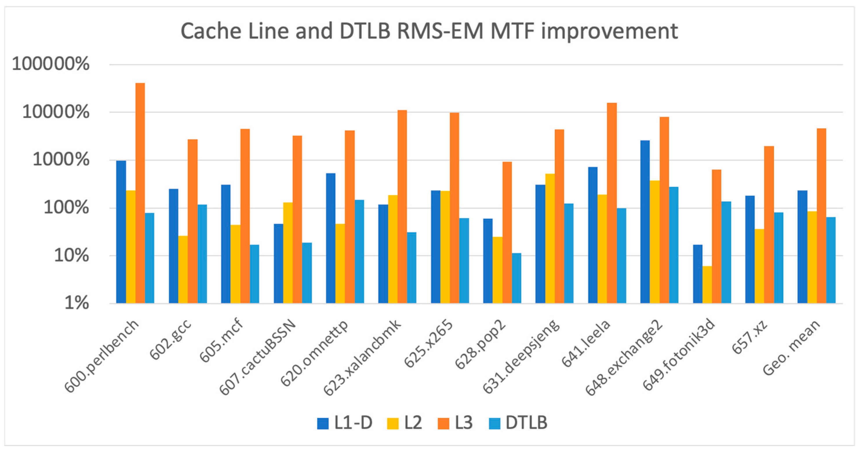
In this section, we present our experimental analysis, which is devoted to examining the RMS-EM MTF improvement for TLBs and cache memory data lines. The results illustrated in Figure 8 show that, in most cases, RMS-EM stress was significantly reduced as a result of the repetitive rotation of the set mapping and invalidation. This helped distribute write operations uniformly over all sets and ways. For the DTLB, we suggested triggering the rotation either when the TLB was flushed by the system or by performing a period rotation (e.g., every 10 million TLB accesses). For the L1-D cache, we suggested a similar periodic rotation trigger every 10 million accesses. For all these options, the performance overhead was minimal. As previously discussed, for both L2 and L3, we suggested triggering the set rotation upon each system wakeup from sleep mode. In this case, no performance overhead was incurred. In our simulation, we used an interval of 10 million cache accesses, which was the same trigger duration of the L1-D cache for both the L2 and L3 caches.
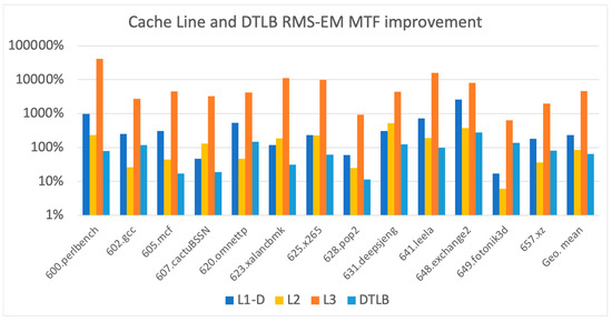
Figure 8.
Cache lines RMS-EM MTF improvement.
Figure 8 illustrates the RMS-EM MTF improvement for the DTLB, L1-D, L2, and L3 caches. The geometric mean MTF improvement for the DTLB, L1-D, L2, and L3 caches was 65%, 230%, 86%, and 4670%, respectively. It can be noted that the experimental results of the EM-aware architectural solution are consistent with the results presented in Section 3. These figures suggest that a smaller ratio of the average number of write operations to the maximum number of writes corresponded to greater RMS-EM MTF improvement.
According to the experimental findings, our proposed solution suggests that the MTF of RMS-EM can be significantly increased in the memory hierarchy elements of microprocessors, ranging from 65% to 4670%. In addition, the proposed EM-aware solution enables microprocessor designers to considerably relax the maximum toggle rate, thereby preventing a substantial number of potential RMS-EM violations.
On the other hand, the decrease in the maximum toggle rate resulted in the extended lifespan of the device. Since the RMS-EM MTF and device lifetime were influenced by both the toggle rate and the thermal and electrical properties of the circuit, we expanded our experimental analysis by conducting physical simulations to account for the Joule heating effect and switching probability.
5.2. Physical RMS-EM Simulations
The final stage of our experimental analysis comprised comprehensive physical simulations incorporating both the Joule heating effect and switching probability. The experimental simulations were conducted using the VoltusTM EM tool [30], a widely accepted tool by the industry and research communities for EM analysis. VoltusTM takes into consideration various transistor parameters, including channel length, channel width, and drive strength. Detailed calculations of the RMS current were made by the tool to examine the effect of self-heating and Joule heating on all signal nets while considering the wire type and geometry (excluding power-grid connections). Through the physical simulations, VoltusTM assumed junction temperature (Tj) of 105 °C and thermal oscillations of +/−5 °C. These thermal conditions represented typical industry sign-off conditions for mission-critical systems and followed foundry guidelines ([24,25,30]). VoltusTM ensured that the analyzed RMS current of each net adhered to the maximum RMS current (IRMS_MAX), which is an essential reliability requirement enforced in the technology file provided by the foundry [31].
To conduct simulations using the VoltusTM environment, it is necessary to perform the synthesis and place-and-route of the examined design. In this study, we examined, as a case study, the L1 data cache memory. The L1 data cache CPU interface assumed a single cycle access for the cache hit and consisted of the following signals:
- An address bus from the CPU to the cache, which specifies the address of the memory access.
- A data output bus from the CPU to the cache for the data to be written by the CPU to the cache.
- A data input bus to the CPU for the data to be read by the CPU from the cache.
- Control signals such as valid, ready, read/write, and hit indication.
Table 3 provides a summary of the implementation tools, design parameters, and simulation environment used in our study. Through the analysis made by VoltusTM, the tool calculated the RMS current (IRMS) for every signal net while considering the switching probability determined from Sniper functional simulations.

Table 3.
Design and simulation tool parameters.
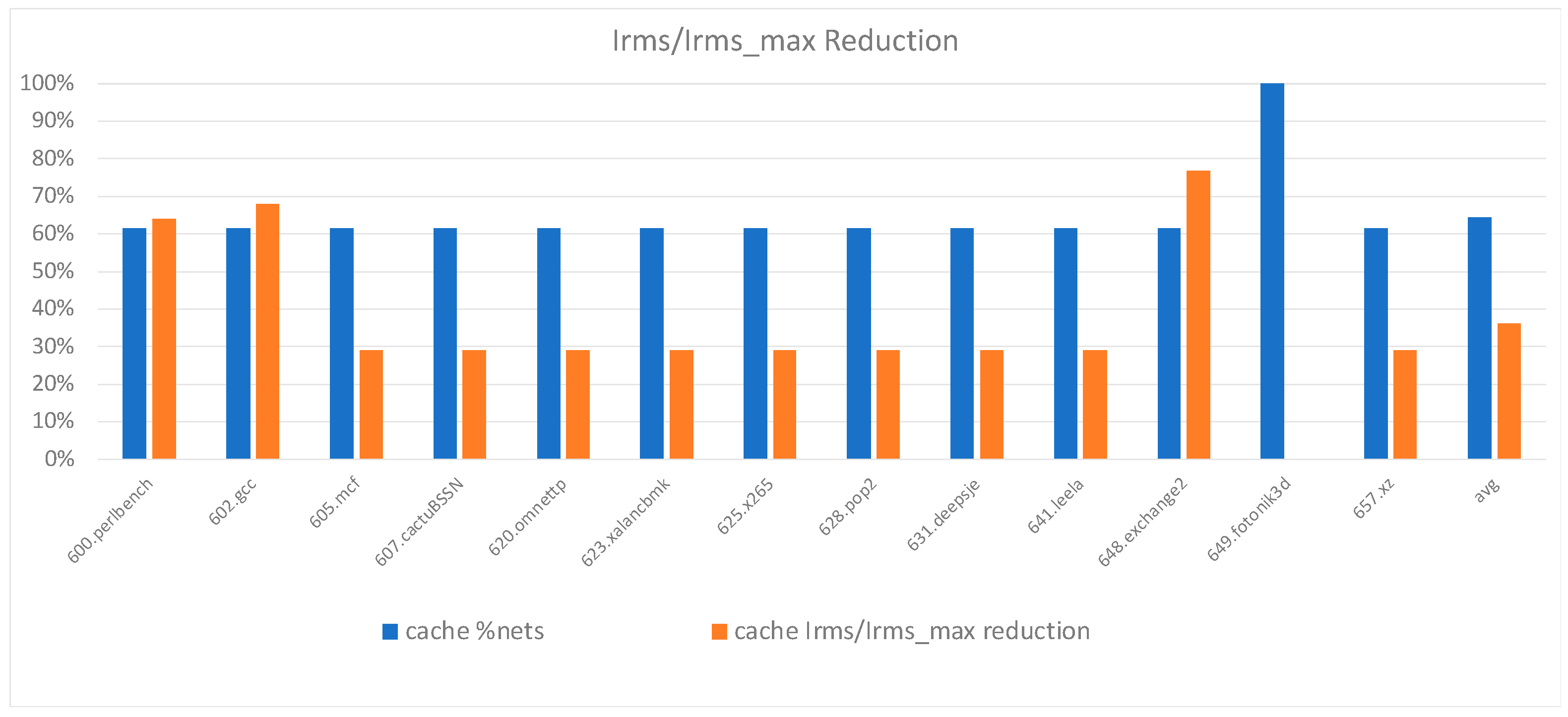
The data presented in Figure 9 compared the IRMS to the IRMS_MAX ratio in EM-aware cache memory architecture with the original design across various benchmarks. It also depicted the percentage of signal nets that could benefit from this reduction in the RMS current. These findings suggest that, on average, 62% of cache memory nets could achieve a 36% reduction in their RMS current. In addition, it was important to indicate that the interconnect nets with no RMS current reduction already had a low RMS current, and therefore, their overall improvement was negligible. The physical simulations presented in Figure 9 were conducted with a 2.66 MHz clock frequency, as indicated by Table 3. It should be noted that the RMS current was dependent on the clock frequency, which, in turn, affected the ratio of IRMS to IRMSrms_max and the potential MTF improvement. Modern microprocessors operating at higher frequencies can significantly leverage our proposed method to reduce RMS EM-related hotspots and significantly extend their lifetime. Conversely, for processors operating at lower frequencies where the RMS current was significantly lower than the maximum RMS current, the impact of hotspots on their lifetime was relatively minimal.
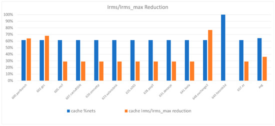
Figure 9.
L1-D Cache IRMS/IRMS-Max ratio decrease achieved by the EM-aware architecture.
Equation (4) [18] can be used to calculate the extended MTF resulting from the reduction in IRMS:
where MTFTechnology is the nominal MTF defined by the foundry [31], which is typically assumed to be 10 years, and IRMS-max is the maximum RMS current to comply with MTFTechnology. The MTFextended represents the extended MTF when the RMS current was reduced to IRMS-reduced. The reduction in the RMS current offered a minimum ×2.5-lifetime extension for cache memories, as the extended MTF was directly proportional to the square of the ratio of IRMS_MAX and to the reduced IRMS. It is worth noting that the experimental results obtained through the RMS-EM physical simulation for the extended MTF were comparable to the MTF improvement prediction in Figure 8, which was based on the reduction in the switching probability.
6. Conclusions
The reliability of memory hierarchy is crucial and poses significant physical-design challenges. Conventionally, RMS-EM reliability-related issues are addressed at the physical implementation stage, assuming worst-case conditions to identify and resolve violations. However, in this study, we proposed a microarchitectural solution that was RMS-EM-aware and could alleviate the overdesign inherent in traditional methods, thus extending a microprocessor’s lifetime. We highlight that modern memory systems are vulnerable to RMS-EM due to their use of non-EM-aware microarchitectures in handling dynamic workloads. To tackle this problem, we put forward architectural solutions that could consider the impact of RMS-EM and aimed to minimize the excessive toggling of memory hierarchy elements. Our proposed solution advocates the use of the proposed RMS-EM-aware resource allocation to evenly distribute write operations across all memory elements. This approach complements existing physical design-based approaches. Based on our analysis, it is evident that our proposed solutions resulted in a minimal area and power overhead, with negligible performance impact compared to previous studies. Our experimental findings indicate that our proposed architectural solution demonstrated a substantial relaxation of the RMS-EM toggle rate sign-off conditions for data blocks throughout the memory system, ranging from 65% to 4670%. Such relaxation offers a 36% reduction in IRMS for an L1 D-cache memory, translating to a lifetime extension of at least 2.5×.
Author Contributions
Conceptualization, F.G. and A.M.; methodology, F.G.; software, F.G.; validation, F.G. and A.M.; formal analysis, F.G.; investigation, F.G.; resources, F.G.; data curation, F.G.; writing—original draft preparation, F.G.; writing—review and editing, F.G. and A.M.; visualization, F.G.; supervision, F.G. and A.M.; project administration, F.G. All authors have read and agreed to the published version of the manuscript.
Funding
This research received no external funding.
Data Availability Statement
Not applicable.
Conflicts of Interest
The authors declare no conflict of interest.
References
- Xuan, X. Analysis and Design of Reliable Mixed-Signal CMOS Circuits. Ph.D. Thesis, Georgia Institute of Technology, Department of Electrical and Computer Engineering, Atlanta, GA, USA, 2004. [Google Scholar]
- Lienig, J.; Jerke, G. Embedded Tutorial: Electromigration-Aware Physical Design of Integrated Circuits. In Proceedings of the 18th International Conference on VLSI Design Held Jointly with 4th International Conference on Embedded Systems Design, Kolkata, India, 3–7 January 2005; IEEE Press: New York, NY, USA, 2005; pp. 77–82. [Google Scholar]
- Lienig, J. Introduction to electromigration-aware physical design. In Proceedings of the International Symposium on Physical Design (ISPD’06), New York, NY, USA, 9–12 April 2006; ACM: New York, NY, USA; pp. 39–46. [Google Scholar]
- Maiz, J.A. Characterization of electromigration under bidirectional (BC) and pulsed unidirectional (PDC) currents. In Proceedings of the 27th Annual Proceedings., International Reliability Physics Symposium, Phoenix, AZ, USA, 11–13 April 1989; pp. 220–228. [Google Scholar]
- Jonggook, K.; Tyree, V.C.; Crowell, C.R. Temperature gradient effects in electromigration using an extended transition probability model and temperature gradient free tests. I. Transition probability model. In Proceedings of the 1999 IEEE International Integrated Reliability Workshop Final Report (Cat. No. 99TH8460), Lake Tahoe, CA, USA, 18–21 October 1999; pp. 24–40. [Google Scholar] [CrossRef]
- Yu, X.; Weide, K. A study of the thermal-electrical- and mechanical influence on degradation in an aluminum-pad structure. Microelectron. Reliab. 1997, 37, 1545–1548. [Google Scholar] [CrossRef]
- Lienig, J. Electromigration and Its Impact on Physical Design in Future Technologies. In Proceedings of the 2013 ACM International Symposium on Physical Design, Stateline, NV, USA, 24–27 March 2013. [Google Scholar]
- Srinivasan, J.; Adve, S.; Bose, P.; Rivers, J. Lifetime Reliability: Toward an Architectural Solution. IEEE Micro. 2005, 25, 70–80. [Google Scholar] [CrossRef]
- Srinivasan, J.; Adve, S.V.; Bose, P.; Rivers, J.A. Exploiting Structural Duplication for Lifetime Reliability Enhancement. ACM SIGARCH Comput. Arch. News 2005, 33, 520–531. [Google Scholar] [CrossRef]
- Dasgupta, A.; Karri, R. Electromigration Reliability Enhancement Via Bus Activity Distribution. In Proceedings of the 33rd Design Automation Conference Proceedings, Las Vegas, NV, USA, 3–7 June 1996; pp. 353–356. [Google Scholar]
- Abella, J.; Vera, X.; Ergin, O.; González, A.; Tschanz, J.W. Refueling: Preventing Wire Degradation due to Electromigration. IEEE Micro. 2008, 28, 37–46. [Google Scholar] [CrossRef]
- Tao, J.; Chen, J.; Cheung, N.; Hu, C. Modeling and characterization of electromigration failures under bidirectional current stress. IEEE Trans. Electron Devices 1996, 43, 800–808. [Google Scholar]
- Abella, J.; Vera, X. Electromigration for Microarchitects. ACM Comput. Surv. 2010, 42, 1–18. [Google Scholar] [CrossRef]
- Calimera, A.; Loghi, M.; Macii, E.; Poncino, M. Dynamic Indexing: Leakage-Aging Co-Optimization for Caches. IEEE Trans. Comput. Des. Integr. Circuits Syst. 2014, 33, 251–264. [Google Scholar] [CrossRef]
- Wang, J.; Dong, X.; Xie, Y.; Jouppi, N.P. i2WAP: Improving non-volatile cache lifetime by reducing inter- and intra-set write variations. In Proceedings of the 2013 IEEE 19th International Symposium on High Performance Computer Architecture (HPCA), Shenzhen, China, 23–27 February 2013; pp. 234–245. [Google Scholar] [CrossRef]
- Tavana, M.K.; Ziabari, A.K.; Arjomand, M.; Kandemir, M.; Das, C.; Kaeli, D. REMAP: A reliability/endurance mechanism for advancing PCM. In Proceedings of the International Symposium on Memory Systems (MEMSYS ’17), New York, NY, USA, 2–5 October 2017; Association for Computing Machinery: New York, NY, USA; pp. 385–398. [Google Scholar] [CrossRef]
- Black, J. Electromigration—A brief survey and some recent results. IEEE Trans. Electron. Devices 1969, 16, 338–347. [Google Scholar] [CrossRef]
- Kahng, A.B.; Nath, S.; Rosing, T.S. On Potential Design Impacts of Electromigration Awareness. In Proceedings of the 2013 18th Asia and South Pacific Design Automation Conference (ASP-DAC), Yokohama, Japan, 22–25 January 2013. [Google Scholar]
- Scorzoni, A.; Neri, B.; Caprile, C.; Fantini, F. Electromigration in thin-film interconnection lines: Models, methods and results. Mater. Sci. Rep. 1991, 7, 143–220. [Google Scholar] [CrossRef]
- Valero, A.; Miralaei, N.; Petit, S.; Sahuquillo, J.; Jones, T.M. On Microarchitectural Mechanisms for Cache Wearout Reduction. IEEE Trans. Very Large Scale Integr. (VLSI) Syst. 2017, 25, 857–871. [Google Scholar] [CrossRef]
- Hau-Riege, C.S. An introduction to Cu electromigration. Microelectron. Reliab. 2004, 44, 195–205. [Google Scholar] [CrossRef]
- Wang, S.; Kim, T.; Sun, Z.; Tan, S.X.-D.; Tahoori, M.B. Recovery-Aware Proactive TSV Repair for Electromigration Lifetime Enhancement in 3-D ICs. IEEE Trans. Very Large Scale Integr. (VLSI) Syst. 2017, 26, 531–543. [Google Scholar] [CrossRef]
- Srinivasan, J.; Adve, S.V.; Bose, P.; Rivers, J.A. The Case for Lifetime Reliability-Aware Microprocessors. In Proceedings of the 31st Annual International Symposium on Computer Architecture, Munich, Germany, 19–23 June 2004. [Google Scholar]
- Gabbay, F.; Mendelson, A. Electromigration-aware Instruction Execution for Modern Microprocessors. In Proceedings of the 4th International Conference on Microelectronic Devices and Technologies (MicDAT ‘2022), Corfu, Greece, 21–23 September 2022; pp. 60–66, ISBN 978-84-09-43856-3. [Google Scholar]
- Gabbay, F.; Mendelson, A. Electromigration-Aware Architecture for Modern Microprocessors. J. Low Power Electron. Appl. 2023, 13, 7. [Google Scholar] [CrossRef]
- Carlson, T.E.; Heirman, W.; Eeckhout, L. Sniper: Exploring the level of abstraction for scalable and accurate parallel multi-core simulations. In Proceedings of the International Conference for High Performance Computing, Net-Working, Storage and Analysis, Seattle, WA, USA, 12–18 November 2011. [Google Scholar]
- Thomadakis, M.E. The Architecture of the Nehalem Processor and Nehalem-EP Smp Platforms. Technical Report. 2010. Available online: http://sc.tamu.edu/systems/eos/nehalem.pdf (accessed on 5 July 2023).
- Limaye, A.; Adegbija, T. A workload characterization of the spec cpu2017 benchmark suite. In Proceedings of the 2018 IEEE International Symposium on Performance Analysis of Systems and Software (ISPASS), Belfast, UK, 2–4 April 2018; pp. 149–158. [Google Scholar]
- Wu, Q.; Flolid, S.; Song, S.; Deng, J.; John, L.K. Invited Paper for the Hot Workloads Special Session Hot Regions in SPEC CPU2017. In Proceedings of the 2018 IEEE International Symposium on Workload Characterization (IISWC), Raleigh, NC, USA, 30 September–2 October 2018. [Google Scholar] [CrossRef]
- VoltusTM User Guide. Available online: http://www.cadence.com (accessed on 5 July 2023).
- LEF DEF Reference. Available online: http://www.si2.org/openeda.si2.org/ (accessed on 5 July 2023).
Disclaimer/Publisher’s Note: The statements, opinions and data contained in all publications are solely those of the individual author(s) and contributor(s) and not of MDPI and/or the editor(s). MDPI and/or the editor(s) disclaim responsibility for any injury to people or property resulting from any ideas, methods, instructions or products referred to in the content. |
© 2023 by the authors. Licensee MDPI, Basel, Switzerland. This article is an open access article distributed under the terms and conditions of the Creative Commons Attribution (CC BY) license (https://creativecommons.org/licenses/by/4.0/).


