Article

Wideband Cascaded and Stacked Receiver Front-Ends Employing an Improved Clock-Strategy Technique

École de Technologie Supérieure (ÉTS), Montreal, QC H3C 1K3, Canada
*
Author to whom correspondence should be addressed.
Current address: Department of Electrical Engineering, École de Technologie Supérieure ÉTS, Montreal, QC H3C 1K3, Canada.
J. Low Power Electron. Appl. 2023, 13(1), 14; https://doi.org/10.3390/jlpea13010014
Submission received: 24 November 2022 / Revised: 27 January 2023 / Accepted: 30 January 2023 / Published: 2 February 2023
(This article belongs to the Special Issue Ultra-Low-Power ICs for the Internet of Things)

Abstract

:
A wideband cascaded receiver and a stacked receiver using an improved clock strategy are proposed to support the software-defined radio (SDR). The improved clock strategy reduces the number of mixer switches and the number of LO clock paths required to drive the mixer switches. This reduces the dynamic power consumption. The cascaded receiver includes an inverter-based low-noise transconductance amplifier (LNTA) using a feed-forward technique to enhance the noise performance; a passive mixer; and an inverter-based transimpedance amplifier (TIA). The stacked receiver architecture is used to reduce the power consumption by sharing the current between the LNTA and the TIA from a single supply. It utilizes a wideband LNTA with a capacitor cross-coupled (CCC) common-gate (CG) topology, a passive mixer to convert the RF current to an IF current, an active inductor (AI) and a 1 / f noise-cancellation (NC) technique to improve the noise performance, and a TIA to convert the IF current to an IF voltage at the output. Both cascaded and stacked receivers are simulated in 22  n m CMOS technology. The cascaded receiver achieves a conversion-gain from 26  d B to 36 d B , a double-sideband noise-figure (NFDSB) from 1.4   d B to 3.9   d B , S 11 < 10   d B and an IIP3 from 7.5   d Bm to 10.5   d Bm , over the RF operating band from 0.4   G Hz to 12  G Hz . The stacked receiver achieves a conversion-gain from 34.5   d B to 36  d B , a NFDSB from 4.6   d B to 6.2   d B , S 11 < 10   d B , and an IIP3 from 21   d Bm to 17.5   d Bm , over the RF operating band from 2.2   G Hz to 3.2   G Hz . The cascaded receiver consumes 11 m from a 1  V supply voltage, while the stacked receiver consumes 2.4 m from a 1.2   V supply voltage.

1. Introduction

Wireless standards operate over a wide frequency spectrum spanning tens of GHz and employ various modulation schemes. Wireless applications have led to the rapid growth of wireless devices in all sectors of the internet of things (IoT), such as health monitoring, agriculture, and smart cities. A wideband system such as the software defied radio (SDR) is a well-suited architecture to address several wireless standards in a single receiver module. Conventional SDRs required a high specification analog-to-digital converters (ADCs), which increased the power consumption and complexity of the design [1] . In [2], down conversion is proposed to reduce the power consumption.
In wideband operation, the wanted signal at the local oscillator (LO) frequency down-converts to the baseband, along with other components of the LO harmonics. This degrades the error vector magnitude (EVM) performance. Harmonic recombination using the N-path receiver architecture is employed to overcome this problem [3,4,5,6]. One of the drawbacks of N-path receivers is that they require a high-frequency driving clock (e.g., 8× the LO frequency) to generate the clock phases that are needed to down-convert the signal at the desired LO frequency, and they reject the harmonics of the LO signal . Similarly, the N-path passive mixer-first topologies that offer input matching without using external components and high-quality filtering can be used [7,8,9]. However, they consume high power to achieve a low noise figure (NF). In addition, mixer-first topologies are not suitable for wideband applications. An N-path ultra-low-power mixer-first receiver is presented in [10]. Although very low power consumption is achieved, it requires an off-chip inductor and achieves a low modulation bandwidth of 3.5 MHz. A feed-forward technique with tuned LO phase was employed in [11] to reject the LO harmonics. However, the phase-correction circuit increases the complexity of the design and reduces accuracy. A harmonic recombination technique that down-converts the signal at 3× the LO frequency is used in [12]. This technique removes all of the other harmonics at the LO frequencies such as the 1st, 2nd, 4th, and 5th harmonics. However, it consumes a significant amount of power in the baseband harmonic recombination circuitry. In addition, it uses a low noise transconductance amplifier (LNTA) with two inductors that occupy a relatively large area. Our earlier work [13] overcame the problems mentioned above. It employed a clock strategy technique to down-convert the signal at 4× the LO frequency while removing all of the other harmonics at the LO frequencies (i.e., 1st , 2nd, 3rd, 5th, 6th, and 7th harmonics). To reduce the power consumption, a current-reuse receiver topology was used. It employed the common-gate LNTA topology with a single to differential balun. In addition, an active inductor was used to improve the receiver sensitivity at higher RF. However, the clock strategy technique proposed in that prior work can be improved to reduce the mixer design complexity and the number of switches. In addition, the technique suffers from low-frequency noise due to the direct coupling of the LNTA noise to the output through the active inductor (AI).
To overcome the limitations mentioned above, this work proposes an improved clock strategy technique that reduces the number of mixer switches and the number of LO clock paths required to drive the mixer switches. This reduces the dynamic power consumption. The clock strategy technique down-converts an RF signal at 4× the LO frequency. The proposed clock strategy is verified through simulations in both cascaded and stacked receiver front-ends. In the cascade receiver front-end, very high RF bandwidth, low noise figure, and good linearity are achieved compared to the stacked receiver front-end at the cost of higher power consumption. The 1 / f noise problem of [13] is resolved in this work by using a 1 / f noise-cancellation (NC) technique. Current mode harmonic recombination is used to reduce the power consumption by avoiding the use of additional harmonic recombination circuitry.
The paper presents the clock strategy in Section 2, the cascaded receiver front-end design and its simulation results in Section 3, the stacked receiver front-end design and its simulation results in Section 4, and the comparison and discussion in Section 5. This is followed by a conclusion.

2. Clock Strategy Technique

The harmonic recombination technique has been used for wideband receiver front-ends to suppress the harmonics of the LO frequency that they down-convert to the baseband along with unwanted signals and noise. A harmonic rejection mixer using a parallel mixing path with a gain ratio of 1 : 2 : 1 is proposed in [14] to reject the third and fifth harmonics at the cost of using two frequency generator circuits that consume area and power. Another approach [15] achieved higher harmonic rejection using a digital adaptive-interference-cancelling (AIC) technique to enhance harmonic rejection. However, it requires high power. In addition, it requires 4 × the LO frequency to generate 8-phase clocks to down-convert the signal at the LO. In [16], a 32-phase non-overlapping LO clock is used to achieve very good harmonic rejection (HR) after LO clock-phase calibration. However, it consumes 30 m W , and it requires harmonic selective TIAs, which increases the area and power consumption. Figure 1a shows the conventional harmonic recombination technique that down-converts a wanted signal at f L O and rejects all of the LO harmonics (i.e., 2 × f L O , 3 × f L O , …, where f L O = C L K I N / 4 ). This requires a CLKIN signal that is equal to 4× of the LO frequency, increasing the complexity and power draw of the clock generation circuit, due to the high clock frequencies required. To overcome these issues, this work proposes a harmonic recombination technique, shown in Figure 1b, that employs a clock strategy to down-convert the wanted signal at 4 × f L O and reject signals at f L O , 2 × f L O , 3 × f L O , 5 × f L O etc. For instance, using a CLKIN at 10 G Hz , an RF input at 10 G Hz is down-converted to baseband. This relaxes the requirements to design the LO clock generation circuits. Figure 1c shows the circuit diagram of the clock divider to generate 8-phase clocks (PH0, PH45, ..., PH316) for conventional harmonic recombination. OR-gates are used to combine the mentioned clocks to generate LO 1 and LO 2 . The proposed clock strategy technique reduces the number of switches in the mixer to two in comparison to eight in the conventional harmonic recombination technique. This reduces the dynamic power consumption in the LO clock paths. In addition, the simplified LO routing on the chip reduces clock signal leakage to the substrate and improves signal integrity.
To evaluate the proposed recombination strategy, the Fourier series coefficients are calculated using
a 0 = 2 N k = 1 N s [ k ] a n = 2 N k = 1 N s [ k ] . c o s [ 2 π N n k ] b n = 2 N k = 1 N s [ k ] . s i n [ 2 π N n k ]
where N is the pulse period, k is the sample number, n is the harmonic number, and s[k] is the signal given by
s [ k ] = m = 1 M ( 1 ) m P m [ k ] = m = 1 M ( 1 ) m ( u [ k ( m 1 ) π 4 ] u [ k m π 4 ] )
where u[k] is the step function and M is the number of each shifted single pulses. The coefficients are calculated based on (1), where a 0 and a n are zero for all harmonics, and b n for harmonics n = 4 , 12 , . . . , 4 ( 2 i 1 ) is calculated by 16 n π . Table 1 shows the calculated Fourier series coefficients of the proposed harmonic recombination technique for seven harmonics. It also presents the example scenario that a signal at 4 G Hz is down-converted while the other LO harmonics are rejected.

3. Cascaded Receiver Front-End Using the Proposed Clock Strategy

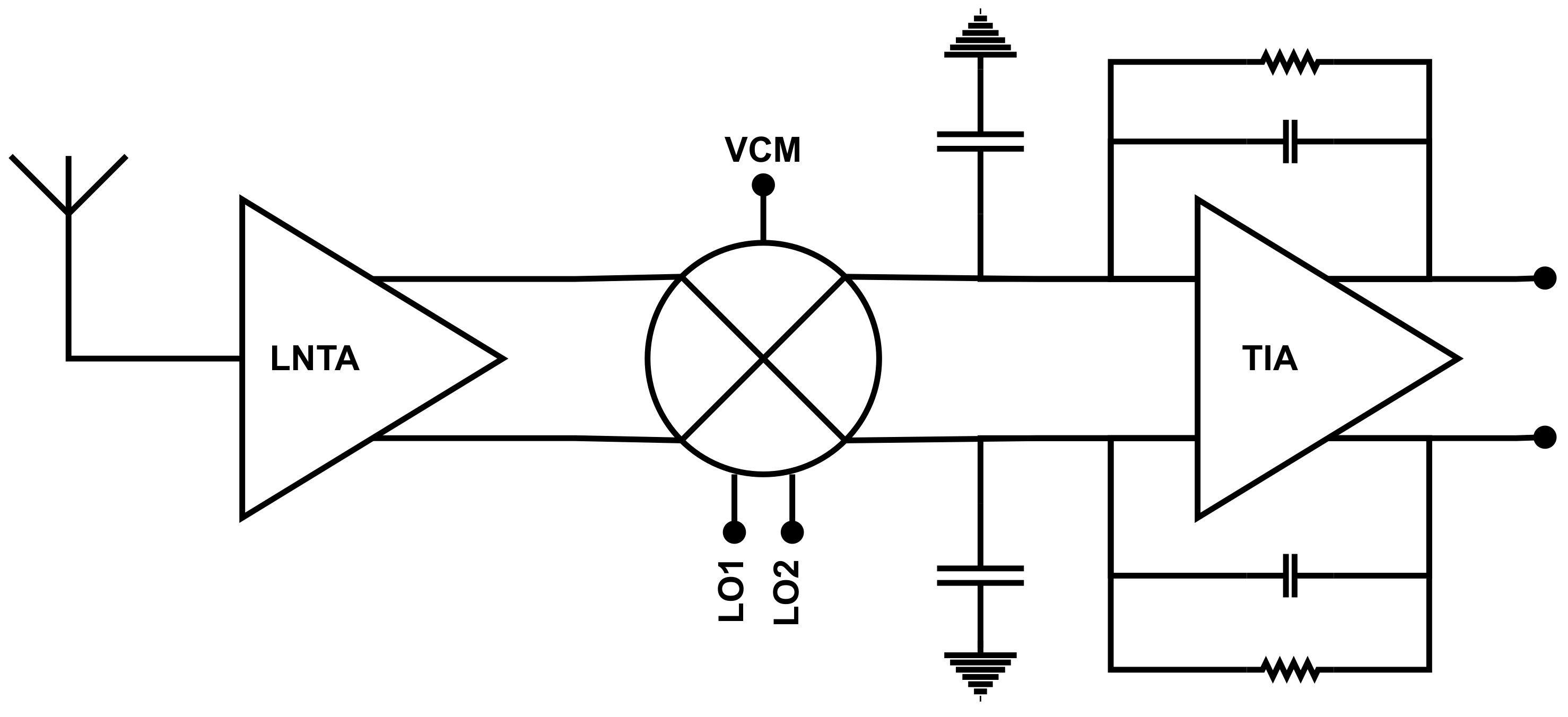
The functionality of the proposed harmonic recombination technique is verified using a cascaded receiver front-end architecture where the LNTA, passive mixer, and TIA are cascaded. Despite previous N-path receiver architectures that use complex and power-consuming circuits to combine the signals at the mixer output [4,17], the proposed receiver performs harmonic recombination in current-mode at the mixer output followed by a single TIA shown in Figure 2.

3.1. LNTA Design

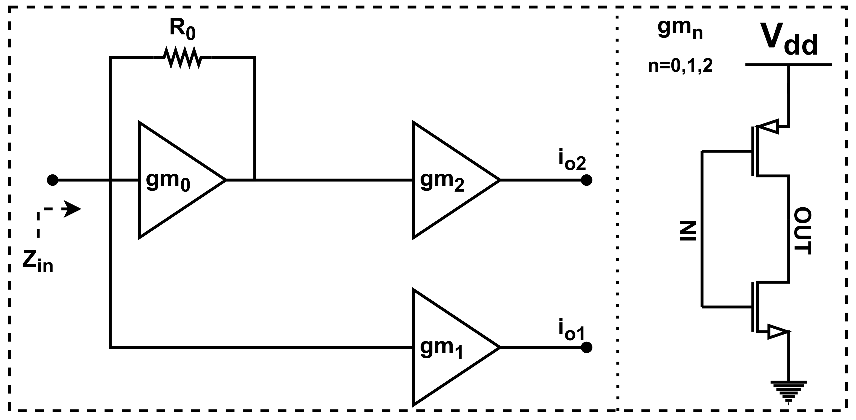
Conventionally, a wideband low noise amplifier (LNA) is used followed by a g m -stage, down-conversion mixer and transimpedance amplifier (TIA). This helps reduce the NF but also amplifies blockers, which can saturate the following stages of the receiver [18]. The LNTA is an alternative that can be used to convert the RF voltage to an RF current that is then down-converted to the IF or BB current through a passive mixer. In this fashion, the receiver is not compressed by blockers due to the inherent low-voltage gain [15]. This work employs a low noise and wideband LNTA proposed in [19], shown in Figure 3.
The first transconductance stage ( g m 0 ) provides the input impedance matching, which is given by
Z i n 1 g m 0 ( 1 + R 0 / r 0 )
where R 0 is the feedback resistor and r 0 is the output resistance of the g m 0 circuit.
Thanks to the feed-forward technique that provides noise-cancellation, the LNTA can achieve a low NF given by
N F 1 + g m 2 g m 1 + λ g m 1 R s
where λ is the short-channel effect coefficient, which can be reduced by increasing the transistor lengths. It can be seen the NF is independent of g m 0 and can be reduced by increasing the g m 1 value.
The total transconductance gain is approximated and given by
G m 1 2 g m 0 R 0 1 1 + R 0 / r 0 g m 2 + g m 1
Transconductance g m 0 provides gate biasing for the g m 1 and g m 2 inverters along with bulk biasing of the PMOS and NMOS transistors since flip-well devices are used in a fully depleted silicon on insulator (FDSOI) CMOS technology. This reduces the area and parasitic capacitance of the AC-coupling capacitors at the input of g m 1 and g m 2 .

3.2. Mixer Design

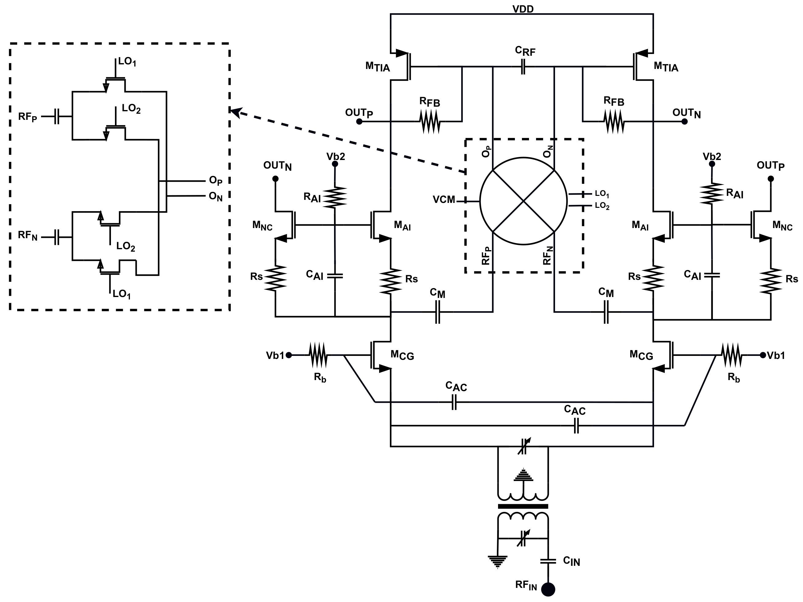
The mixer is responsible for down-converting the RF signal to the IF signal using the LO signal. There are two well-known mixer architectures: the passive and the active mixer. The passive mixer is preferred over the active mixer due to its high linearity performance yielded by the current-mode operation. In the passive mixer, switches are biased in a linear region. The gate of the switches are biased to make sure that the LO signal is able to turn on the mixer switches when it toggles between 0 V and the supply voltage. The circuit diagram of the mixer is shown in Figure 4. The mixer input is ac-coupled using a capacitor to separate the LNTA biasing and block low-frequency noise. The drain and source of the mixer switches are biased by the TIA common-mode voltage.

3.3. TIA Design

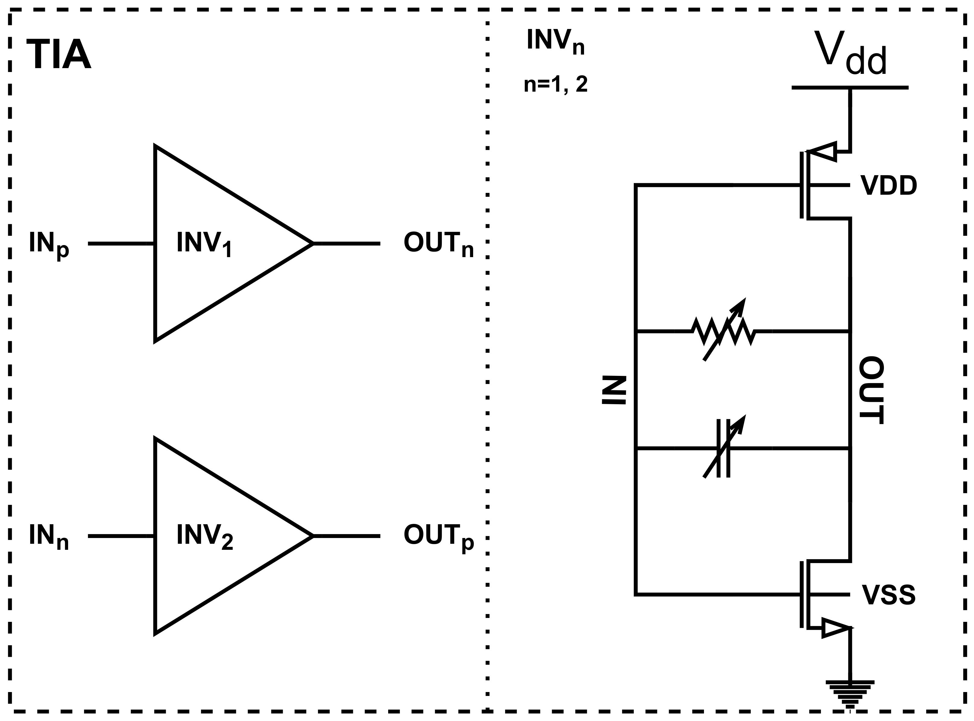
The transimpedance amplifier (TIA) is used after the passive mixer to convert the IF current to an IF voltage at the output. In addition, it provides low-input impedance that improves the linearity. This work employs an inverter-based TIA using a feedback resistor to control the gain and a capacitor bank to define the IF bandwidth, shown in Figure 5. The current reuse inverter using both PMOS and NMOS enhances the overall transconductance without consuming extra power.
The input impedance looking into the I N V n input is given by
Z i n = R g m R o u t + 1 g m
where R is the feedback resistor and g m is given by g m p + g m n .
The conversion-gain of the proposed receiver can be calculated as
C G 2 π S i n ( π d ) 2 d g m R F B
where d is the clock duty-cycle that is 12.5% in this work.

3.4. Simulation Results of the Cascaded Receiver Front-End

The wideband receiver front-end using the clock strategy was designed and simulated in a 22 nm CMOS technology. The receiver consumes 11 mA from a 1 V supply voltage. The LNTA and TIA consume 4 mA and 7 mA, respectively.
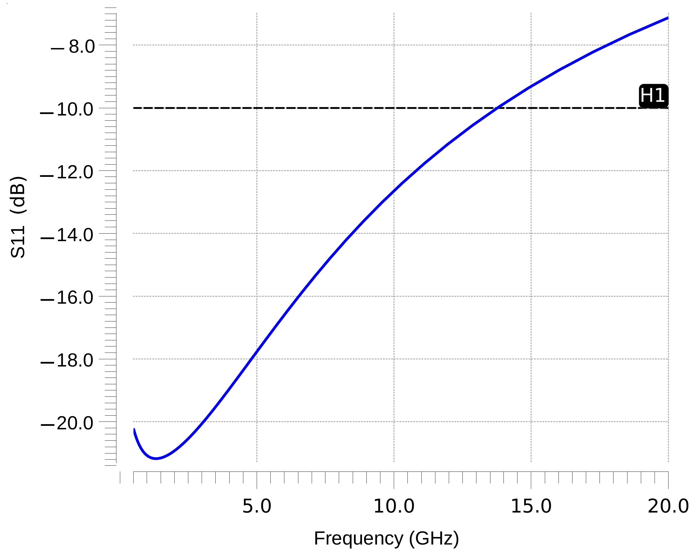
The wideband input matching ( S 11 ) of the LNTA is shown in Figure 6, showing an S 11 of less than 10 d B at up to 13 G Hz , which is suitable for ultra wideband applications.
The receiver-performance, integrated double-sideband noise-figure (NFDSB) from 10 k Hz to 100 MHz, conversion gain and input-referred third-order intercept point (IIP3) versus f L O , which is equivalent to an input RF signal having a frequency of 4 × f L O , from 400 MHz to 12 G Hz , is shown in Figure 7. It shows the NFDSB is increasing in frequency from almost 1.4 d B to 3.9 d B . On the other hand, the conversion gain reduces from almost 36 d B to 26 d B as f L O is increased. A constant value of feedback resistor is used in the TIA. To perform the IIP3 simulation, a two-tone signal at 4 × f L O + 10 MHz and 4 × f L O + 11 MHz is applied at the input of the LNTA. This generates two third-order intermodulation products at 9 MHz and 12 MHz along with two fundamental products at 10 MHz and 11 MHz. The IIP3 performance varies over f L O from 10.5 d Bm to 7.5 d Bm .
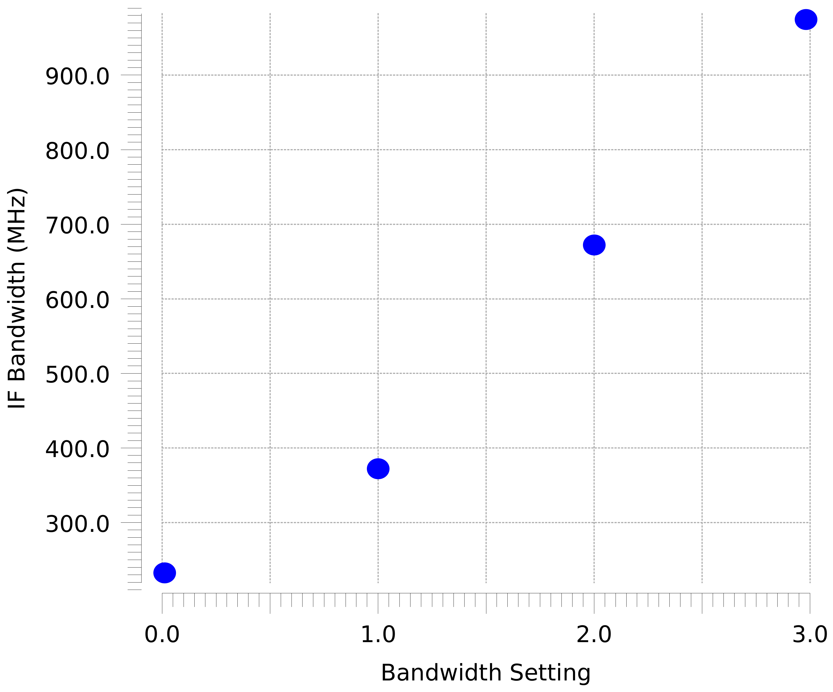
The TIA bandwidth can be configured with four settings using two capacitors. Figure 8 shows the receiver bandwidth can be configured from 250 MHz to almost 1 G Hz . This can be changed using different values of feedback capacitors and also the shunt capacitors after the mixer, which are 2 p F in this work. It shows that the receiver is suitable for very wideband baseband modulation.
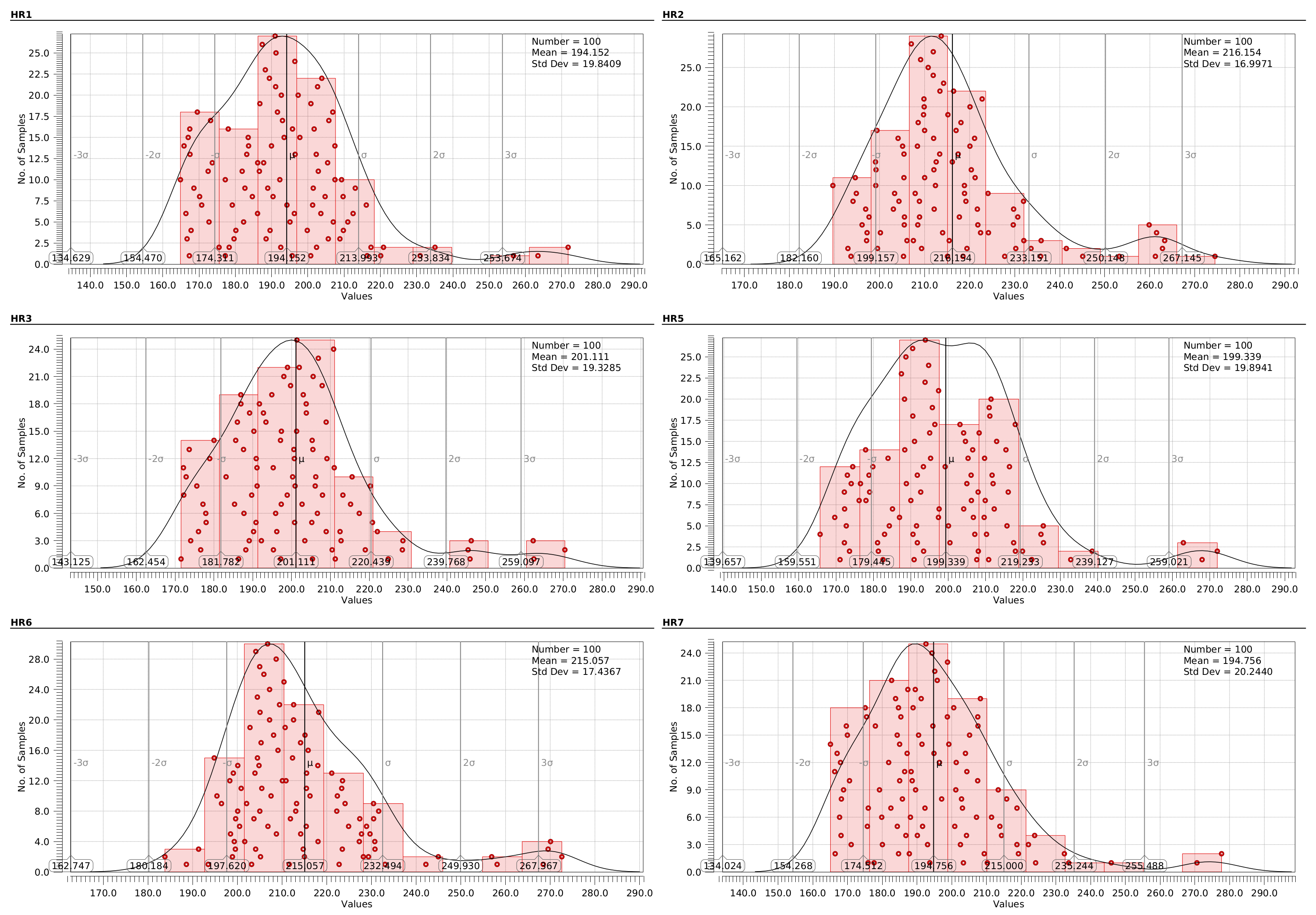
The harmonic rejection can be affected by the transistor process and mismatch variations. The effect of the transistor process and mismatch variation is verified using Monte-Carlo simulation over 100 runs, and the results are shown in Figure 9. The HR1, HR2, … HRn (n = 7) are the 1st, 2nd, … nth harmonics rejected relative to the 4th harmonic, which is the wanted signal in this work. This shows that very good harmonic rejection is achieved at all harmonics with a minimum rejection of 134 d B in HR7 using a 3 × sigma calculation.

4. Stacked Receiver Front-End Using the Proposed Clock Strategy

By scaling down the CMOS technology node, the threshold voltage ( V T H ) is lowered, enhancing the frequency of operation and enabling new low-power design techniques that have emerged. One effective low-power design technique is the current-reuse or stacked technique by means of stacking different circuits such as LNTA, mixer, and TIA to share the biasing current from a single supply. Thus, in the stacked receiver front-end, the LNTA, mixer, and TIA are stacked.
Although this reduces power consumption, it still has drawbacks. The LNA, mixer, and voltage controlled oscillator (VCO) are staked in [20] to improve the power efficiency, but the circuit may suffer from the injection locking of the VCO due to the large blockers. Moreover, it has high NF. An unbalanced single to differential LNA, active mixer, and baseband circuitry are cascoded to reduce power consumption in [21]. However, the active mixer degrades the linearity performance and increases the voltage headroom requirements. A simultaneous input matching and 1 / f NC technique is employed in [22] that results in a very low NF of less than 2 d B . However, the use of the common-source (CS) LNTA topology reduces the RF bandwidth. In addition, due to the receiver topology that connects the mixer input to the output node, the receiver is not able to operate at high frequency. Our earlier works [13,23,24], overcome the problems mentioned above. However, the mixer circuit in [13] needs to be improved to reduce the number of mixer switches. In addition, it suffers from 1 / f noise that does not allow the receiver to operate at low frequency with good NF performance.
To overcome the limitations mentioned above, this work proposes a stacked receiver front-end, shown in Figure 4. It includes an on-chip balun to convert the single-ended antenna to a differential signal at the input of the LNTA, a capacitive cross-coupled common-gate (CG) LNTA topology to convert the RF voltage to an RF current, an active inductor (AI) and a 1 / f noise-cancellation (NC) technique to isolate the mixer input and enhance low-frequency noise performance, a passive mixer to down-convert the RF current to an IF current, and a TIA to convert the IF current to an IF voltage at the output. The TIA and LNTA share the current using a single supply, reducing the power consumption.

4.1. LNTA Design

Two well-known LNTA topologies, common-gate (CG) and common-source (CS), can be used. The CS LNTA is suitable for very-low-noise applications at the cost of a narrow RF bandwidth. It is also very susceptible to non-idealities related to fabrication and packaging. On the other hand, the CG topology is used for wideband matching, and it is more reliable. The input impedance looking into the CG LNTA is 1/gm. Very high current and large device sizes are required to achieve the 1/gm = 50 Ω . To overcome this, a capacitor cross-coupled (CCC) technique is used to boost the effective g m by two times without consuming extra power. It also improves the NF. The LNTA circuit is formed by M CG , R b , and C AC . The noise factor of the LNTA is given by
F = 1 + γ R S × g m ,
where R S is the source impedance and γ is the short-channel effect coefficient, and can be reduced by increasing the transistor lengths.

4.2. Active-Inductor and 1 / f Noise-Cancellation Design

In [22], the mixer input is connected to the output node. This increases the RF signal loss, and it does not allow the circuit to maintain its performance at high RF. To overcome this, the proposed AI circuit isolates the mixer input from the output. The impedance looking into the AI circuit is low at DC, while it increases at RF. In this case, the signal loss is then limited to parasitic capacitors. M AI , C AI , and R AI form the AI circuit. The small R s is used to boost the impedance at high frequencies with minimal impact at low frequencies. The impedance looking into the AI circuit is approximately given by
Z A I ( s ) g m , A I R S ( R A I C A I s + 1 ) + R A I C A I s g m , A I R S C A I s + g m , A I + C A I s 1 s C p a r ,
where C par is the parasitic capacitance at the mixer input.
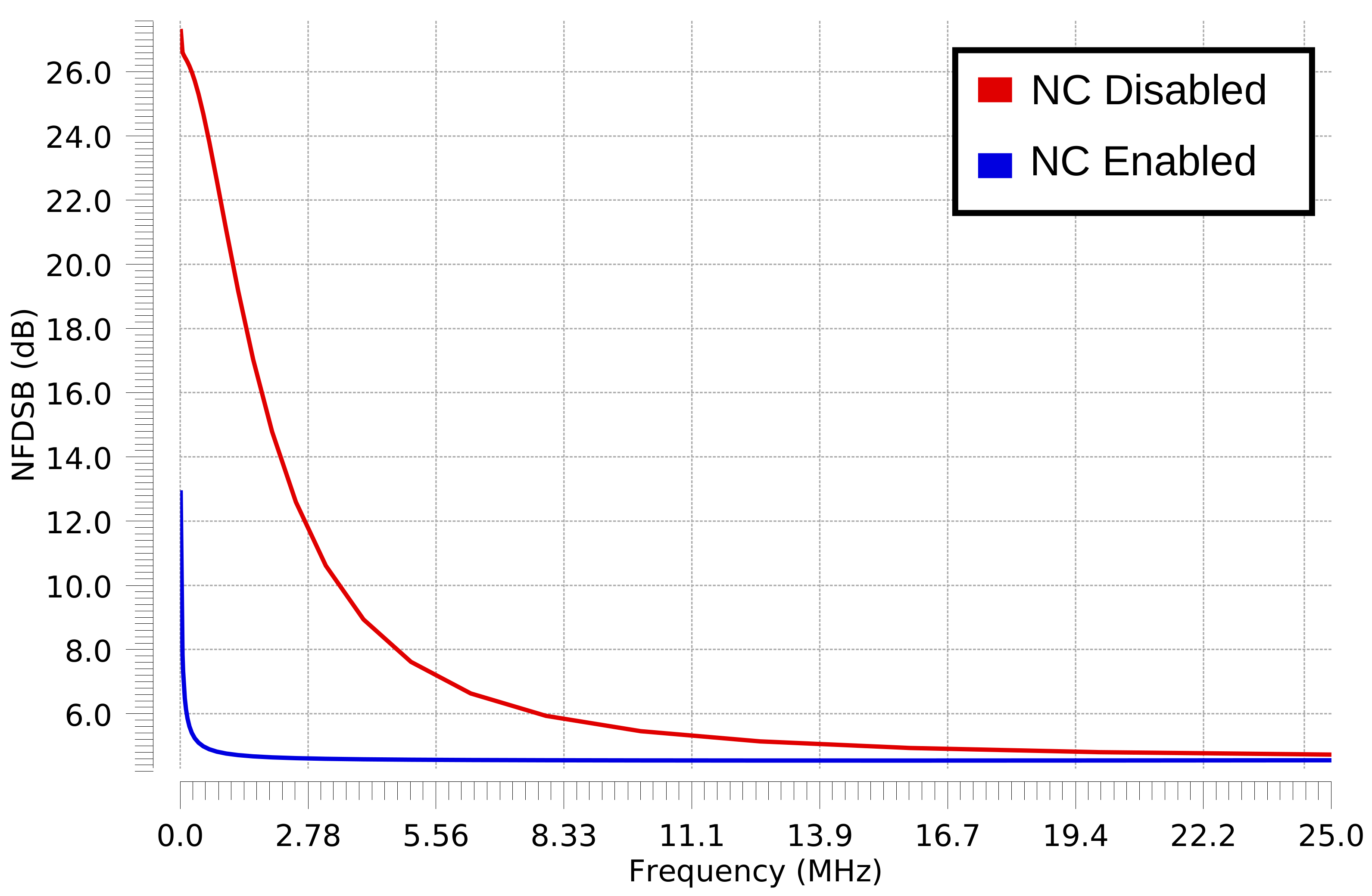
The stacked receiver front-end suffers from high low-frequency noise due to the direct coupling of the noise through the AI circuit. To overcome this issue, a 1 / f NC circuit is formed by the M NC transistors. It provides the signal path to the output with the opposite polarity to cancel the low-frequency noise and push the 1 / f corner to a lower frequency. The functionality of the 1 / f NC circuit is being verified in Figure 10. It shows the 1 / f noise corner is pushed to a very low IF when the 1 / f NC circuit is enabled, while the thermal noise remains almost constant.

4.3. TIA Design

The transimpedance amplifier (TIA) is used to convert the IF current to an IF voltage at the output. The TIA circuit is formed by transistors M TIA and feedback resistors R FB , where an additional harmonic recombination circuit is not required. The length of M TIA should be large enough to enhance the output impedance. The conversion gain of the proposed stacked receiver can be calculated using Equation (7).

4.4. Simulation Results of the Stacked Receiver Front-End

The wideband stacked receiver front-end using a clock strategy was designed and simulated in a 22 nm CMOS technology. The receiver consumes 2.4 mA from a 1.2   V supply voltage.
The wideband input matching ( S 11 ) of the LNTA is shown in Figure 11, showing an S 11 of less than 10 d B over a wide frequency range by switching the capacitor bank at the input balun. The capacitor bank uses 16 binary weighted codes. The rest of the simulations in this work are verified using code 8.
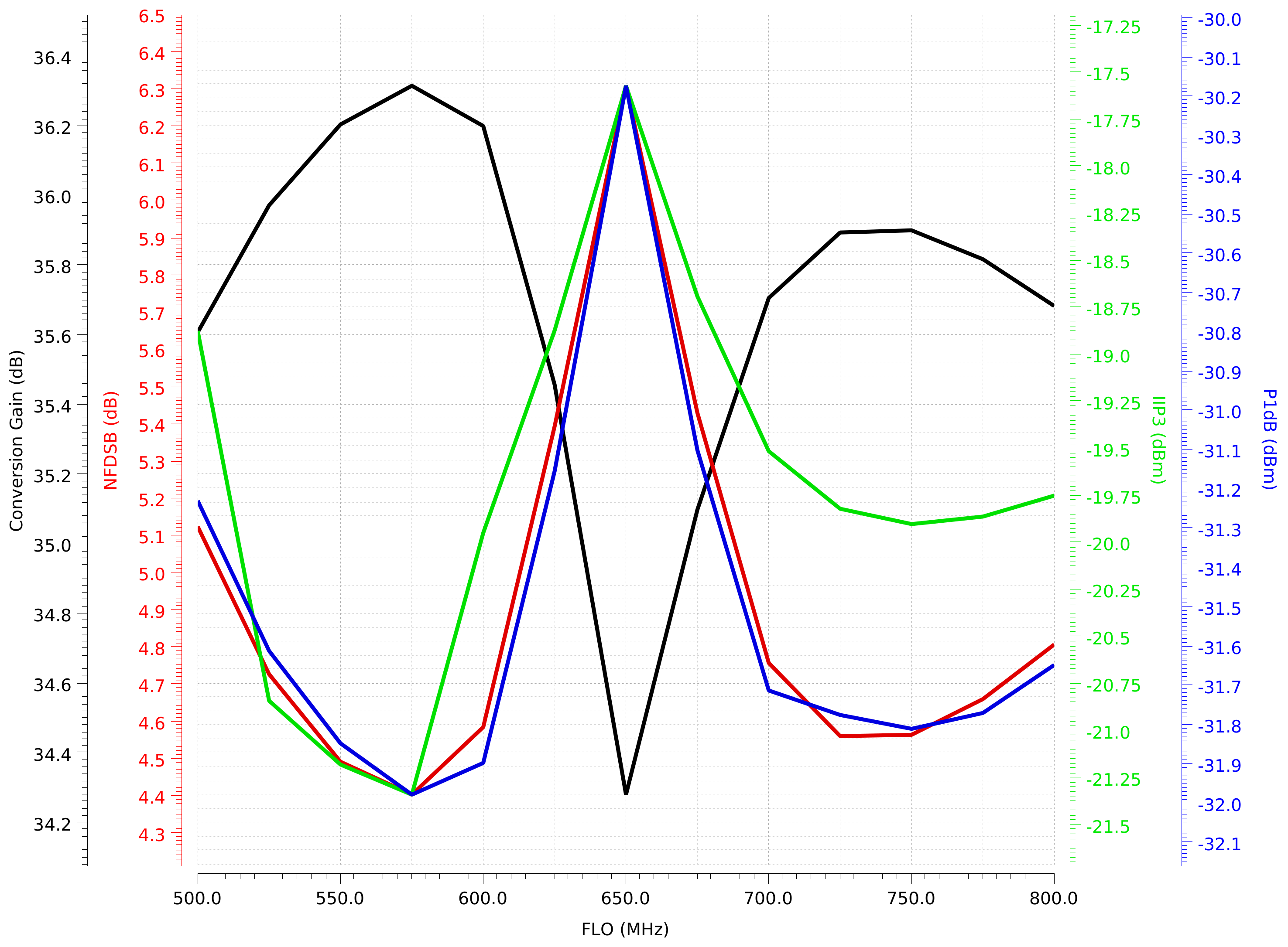
The receiver-performance, integrated NFDSB from 100 k Hz to 50 MHz, conversion gain and input-referred third-order intercept point (IIP3) versus f L O , which is equivalent to an RF input signal of 4 × f L O , from 2.2 G Hz to 3.2 G Hz , is shown in Figure 12. It shows that the NFDSB varies in terms of frequency from almost 4.5 d B to 6.3 d B . On the other hand, the conversion gain varies from almost 34.5 d B to 36 d B as f L O is increased. A constant feedback resistor is used in the TIA. To perform IIP3 simulation, a two-tone signal at 4 × f L O + 10 MHz and 4 × f L O + 11 MHz is applied at the input of the LNTA. This generates two third-order intermodulation products at 9 MHz and 12 MHz, along with two fundamental products at 10 MHz and 11 MHz. The IIP3 performance varies over f L O from 21 d Bm to 17.5 d Bm .
The harmonic rejection can be affected by transistor and layout mismatch. The effect of the transistor process and mismatch variation is verified using Monte-Carlo simulation over 100 runs, and the results are shown in Figure 13. The HR1, HR2, … HRn (n = 7) are the 1st, 2nd, … nth harmonics rejected relative to the 4th harmonic, which is the wanted signal in this work. The harmonic rejection in the stacked receiver front-end architecture is much less than the cascaded receiver architecture. The minimum rejection is achieved in HR5 with a 61 d B rejection using a 3 × sigma calculation.

5. Discussion

Table 2 provides a performance summary and comparison of the cascaded and stacked receiver front-end using the clock strategy proposed in this work and compare them to the state-of-the-art. The cascaded receiver front-end with the clock strategy achieves a higher RF bandwidth, IIP3, and lower NF compared to the staked receiver front-end proposed in this work, while consuming almost four times current but operating at a slightly lower supply voltage of 1 V . The cascaded receiver architecture also achieved a higher RF bandwidth than work in [3,9,16] while consuming much lower power. Overall, both circuits presented in this work are suitable for wide modulation bandwidth application. The NF, IIP3, and bandwidth performance compare well with the state-of-the-art considering the power consumption of the presented receivers. The harmonic recombination technique verified by both receiver architectures validates the viability of the technique for different receiver architectures. The minimum harmonic rejection ratio of the cascaded, stacked receiver, refs [3,4,12,16] are approximately 134, 61, 35, 51, 80, and 52 d B , respectively. The stacked receiver architecture is better suited to very low power wireless applications with relaxed performance requirements such as Bluetooth Low Energy, while the cascaded receiver architecture can be used for a wide range of higher performance applications.

6. Conclusions

Wideband cascaded and stacked receiver front-ends employing a clock strategy to down-convert an RF signal at 4× the f L O frequency were designed in a 22-nm CMOS process for SDR applications. The simulation results are presented showing the benefits of both architectures. The cascaded receiver front-end achieved higher bandwidth, lower NF, and better linearity performance than the stacked receiver front-end at the cost of higher power consumption. In the cascaded receiver front-end, low NF was achieved thanks to the feed-forward noise cancelling technique of the LNTA. The LNTA used by the cascaded receiver front-end operates over a frequency range from 0.4 G Hz to 13 G Hz . In the stacked receiver front-end, the low power consumption was achieved by sharing the current between the TIA and the LNTA using a single supply. The noise performance was also improved by using an AI and 1 / f noise-cancellation technique.
Thanks to the current mode harmonic recombination, both receivers do not require additional circuits for harmonic recombination, reducing the power consumption. Dynamic power consumption is ultimately reduced thanks to the clock strategy technique that down-converts an RF signal at 4 × f L O , reducing the clock frequency requirements. In the stacked receiver architecture, the CCC technique boosts g m by two times without consuming additional power. The LNTA and balun can be tuned over an input frequency range from 2 G Hz to 6 G Hz .
The wideband operation and performance metrics of the proposed front-ends make them very suitable for SDR receivers that require a wideband frequency response and good harmonic rejection performance.

Author Contributions

Conceptualization, A.A. and F.N.; methodology, A.A.; software, A.A.; validation, A.A.; formal analysis, A.A.; investigation, A.A.; resources, A.A.; data curation, A.A.; writing—original draft preparation, A.A.; writing—review and editing, A.A. and F.N.; visualization, A.A.; supervision, A.A. and F.N.; project administration, A.A.; and funding acquisition, F.N. All authors have read and agreed to the published version of the manuscript.

Funding

This research received funding from the Natural Sciences and Engineering Research Council of Canada.

Institutional Review Board Statement

Not applicable

Informed Consent Statement

Not applicable

Data Availability Statement

Not applicable

Acknowledgments

The author would like to thank CMC Microsystems for providing access to the EDA tools.

Conflicts of Interest

The authors declare no conflict of interest.

Abbreviations

The following abbreviations are used in this manuscript:
ADCAnalog-to-digital converter
AIActive inductor
AICAdaptive interference cancelling
CGCommon-gate
CCCCapacitor cross-coupled
CMOSComplementary metal–oxide semiconductor
CSCommon-source
ÉTSÉcole de technologie supérieure
FDSOIFully depleted silicon on insulator
HRHarmonic rejection
IFIntermediate frequency
IIP3Third-order intercept point
IoTInternet of things
LNALow-noise amplifier
LNTALow-noise transconductance amplifier
LOLocal-oscillator
NFNoise figure
NCNoise cancellation
NFDSBDouble side-band noise figure
RFRadio frequency
SDRSoftware-defined radio
TIATransimpedance amplifier
VCOVoltage-controlled oscillator
V TH Voltage-threshold
g m Tranconductance

References

  1. Mitola, J. The software radio architecture. IEEE Commun. Mag. 1995, 33, 26–38. [Google Scholar] [CrossRef]
  2. Ke, Y.; Gao, P.; Craninckx, J.; Van der Plas, G.; Gielen, G. A 2.8-to-8.5 mW GSM/bluetooth/UMTS/DVB-H/WLAN fully reconfigurable CT ΔΣ with 200kHz to 20MHz BW for 4G radios in 90nm digital CMOS. In Proceedings of the 2010 Symposium on VLSI Circuits, Honolulu, HI, USA, 16–18 June 2020; IEEE: Piscataway Township, NJ, USA, 2010; pp. 153–154. [Google Scholar]
  3. Murphy, D.; Darabi, H.; Xu, H. A noise-cancelling receiver resilient to large harmonic blockers. IEEE J. -Solid-State Circuits 2015, 50, 1336–1350. [Google Scholar] [CrossRef]
  4. Lin, F.; Mak, P.I.; Martins, R.P. An RF-to-BB-current-reuse wideband receiver with parallel N-path active/passive mixers and a single-MOS pole-zero LPF. IEEE J. -Solid-State Circuits 2014, 49, 2547–2559. [Google Scholar] [CrossRef]
  5. Elmi, M.; Tavassoli, M.; Jalali, A. A wideband receiver front-end using 1st and 3rd harmonics of the N-path filter response. Analog. Integr. Circuits Signal Process. 2018, 94, 451–467. [Google Scholar] [CrossRef]
  6. Zinjanab, A.P.; Jalali, A.; Farshi, H.T. A standard and harmonic blocker tolerant receiver front-end using a harmonic rejection differential N-path notch filter and blocks withstand to possible variations. AEU-Int. J. Electron. Commun. 2020, 125, 153356. [Google Scholar] [CrossRef]
  7. Andrews, C.; Molnar, A.C. A passive mixer-first receiver with digitally controlled and widely tunable RF interface. IEEE J. -Solid-State Circuits 2010, 45, 2696–2708. [Google Scholar] [CrossRef]
  8. Lien, Y.C.; Klumperink, E.A.; Tenbroek, B.; Strange, J.; Nauta, B. Enhanced-selectivity high-linearity low-noise mixer-first receiver with complex pole pair due to capacitive positive feedback. IEEE J. -Solid-State Circuits 2018, 53, 1348–1360. [Google Scholar] [CrossRef]
  9. Zolkov, E.; Cohen, E. A Mixer-First Receiver With Enhanced Matching Bandwidth by Using Baseband Reactance-Canceling LNA. IEEE Solid-State Circuits Lett. 2021, 4, 109–112. [Google Scholar] [CrossRef]
  10. Mohammadpour, A.; Manstretta, D.; Castello, R. A 140-μW Front-End With 5.7-dB NF and+ 10-dBm OOB-IIP3 Using Voltage-Mode Boosting Mixer. IEEE Microw. Wirel. Components Lett. 2021, 31, 729–732. [Google Scholar] [CrossRef]
  11. Bazrafshan, A.; Taherzadeh-Sani, M.; Nabki, F. A 0.8–4-GHz software-defined radio receiver with improved harmonic rejection through non-overlapped clocking. IEEE Trans. Circuits Syst. Regul. Pap. 2018, 65, 3186–3195. [Google Scholar] [CrossRef]
  12. Shams, N.; Nabki, F. Analysis and Comparison of Low-Power 6-GHz N-Path-Filter-Based Harmonic Selection RF Receiver Front-End Architectures. IEEE Trans. Very Large Scale Integr. (VLSI) Syst. 2022, 30, 253–266. [Google Scholar] [CrossRef]
  13. Abbasi, A.; Moshrefi, A.H.; Nabki, F. A Wideband Low-Power Current-Reuse RF-to-BB Receiver Using a Clock Strategy Technique. In Proceedings of the 2022 20th IEEE Interregional NEWCAS Conference (NEWCAS), Quebec, QC, Canada, 19–22 June 2022; IEEE: Piscataway Township, NJ, USA, 2022; pp. 275–279. [Google Scholar]
  14. Weldon, J.A.; Narayanaswami, R.S.; Rudell, J.C.; Lin, L.; Otsuka, M.; Dedieu, S.; Tee, L.; Tsai, K.C.; Lee, C.W.; Gray, P.R. A 1.75-GHz highly integrated narrow-band CMOS transmitter with harmonic-rejection mixers. IEEE J. -Solid-State Circuits 2001, 36, 2003–2015. [Google Scholar] [CrossRef]
  15. Ru, Z.; Moseley, N.A.; Klumperink, E.A.; Nauta, B. Digitally enhanced software-defined radio receiver robust to out-of-band interference. IEEE J. -Solid-State Circuits 2009, 44, 3359–3375. [Google Scholar] [CrossRef]
  16. Wu, H.; Murphy, D.; Darabi, H. A harmonic-selective multi-band wireless receiver with digital harmonic rejection calibration. IEEE J. -Solid-State Circuits 2019, 54, 796–807. [Google Scholar] [CrossRef]
  17. Xu, Y.; Zhu, J.; Kinget, P.R. A Blocker-Tolerant RF Front End With Harmonic-Rejecting N-Path Filter. IEEE J. -Solid-State Circuits 2017, 53, 327–339. [Google Scholar] [CrossRef]
  18. Bagheri, R.; Mirzaei, A.; Chehrazi, S.; Heidari, M.E.; Lee, M.; Mikhemar, M.; Tang, W.; Abidi, A.A. An 800-MHz–6-GHz software-defined wireless receiver in 90-nm CMOS. IEEE J. -Solid-State Circuits 2006, 41, 2860–2876. [Google Scholar] [CrossRef]
  19. Manetakis, K.; McKay, T.G. Wideband Low Noise Amplifier Having DC Loops with Back Gate Biased Transistors. US Patent 10,700,653, 30 June 2023. [Google Scholar]
  20. Tedeschi, M.; Liscidini, A.; Castello, R. Low-power quadrature receivers for ZigBee (IEEE 802.15. 4) applications. IEEE J. -Solid-State Circuits 2010, 45, 1710–1719. [Google Scholar] [CrossRef]
  21. Lin, Z.; Mak, P.I.; Martins, R.P. A 2.4 GHz ZigBee Receiver Exploiting an RF-to-BB-Current-Reuse Blixer+ Hybrid Filter Topology in 65 nm CMOS. IEEE J. -Solid-State Circuits 2014, 49, 1333–1344. [Google Scholar] [CrossRef]
  22. Kim, S.; Kwon, K. A Low-Power RF-to-BB-Current-Reuse Receiver Employing Simultaneous Noise and Input Matching and 1/f Noise Reduction for IoT Applications. IEEE Microw. Wirel. Components Lett. 2019, 29, 614–616. [Google Scholar] [CrossRef]
  23. Abbasi, A.; Nabki, F. A Design Methodology for Wideband Current-Reuse Receiver Front-Ends Aimed at Low-Power Applications. Electronics 2022, 11, 1493. [Google Scholar] [CrossRef]
  24. Abbasi, A.; Moshrefi, A.H.; Nabki, F. A Wideband Low-Power RF-to-BB Current-Reuse Receiver Using an Active Inductor and 1/f Noise-Cancellation for L-Band Applications. IEEE Access 2022, 10, 95839–95848. [Google Scholar] [CrossRef]
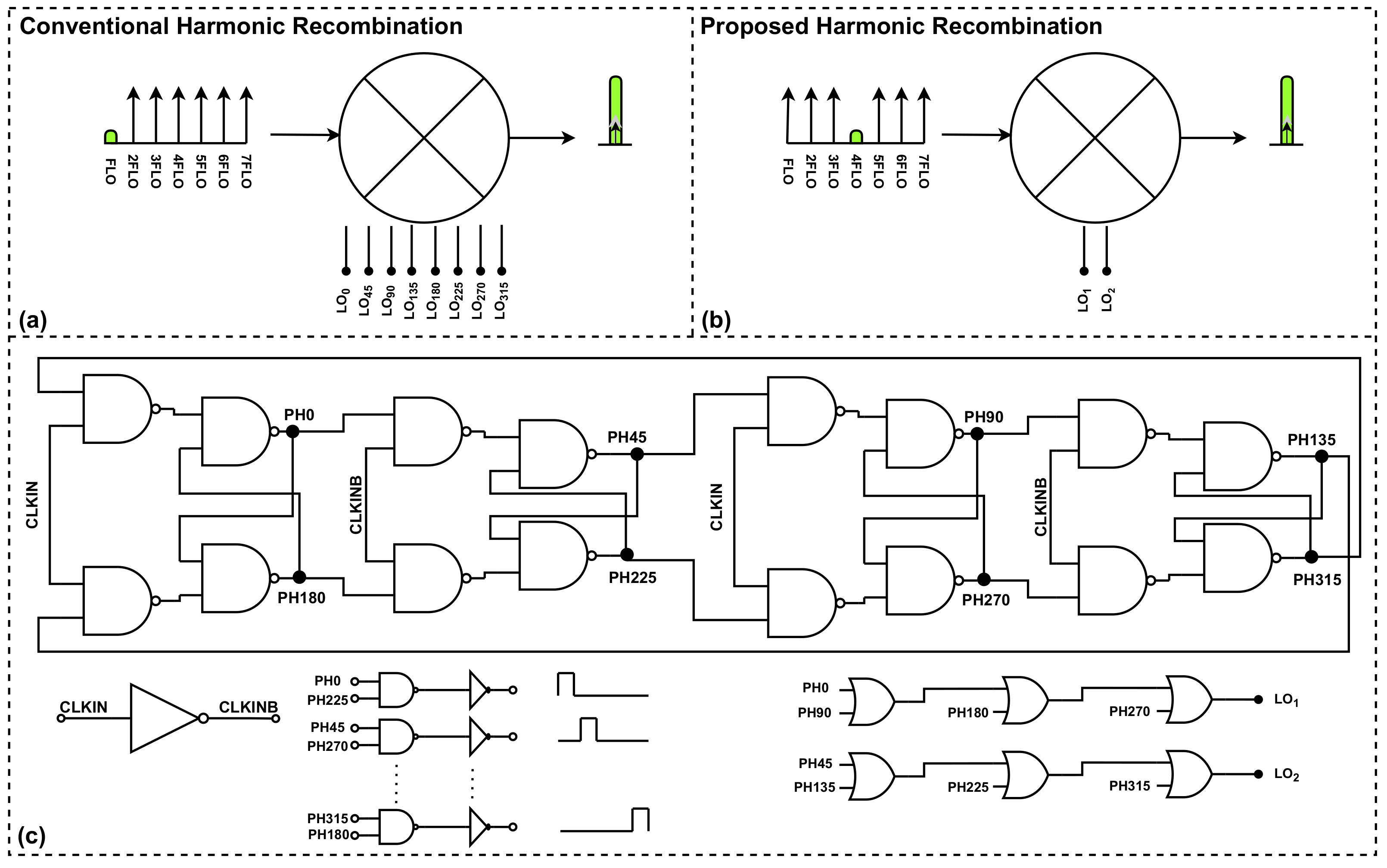
Figure 1. Harmonic recombination techniques: (a) cascaded approach, (b) stacked approach, and (c) clock generation circuitry.
Jlpea 13 00014 g001
Figure 2. Cascaded receiver diagram.
Jlpea 13 00014 g002
Figure 3. LNTA circuit diagram.
Jlpea 13 00014 g003
Figure 4. Stacked receiver circuit diagram.
Jlpea 13 00014 g004
Figure 5. TIA circuit diagram.
Jlpea 13 00014 g005
Figure 6. The cascaded received input matching (S11) performance versus RF.
Jlpea 13 00014 g006
Figure 7. The cascaded receiver NFDSB, conversion gain, and IIP3 performances versus f L O .
Jlpea 13 00014 g007
Figure 8. The cascaded receiver bandwidth versus the bandwidth settings.
Jlpea 13 00014 g008
Figure 9. H R n performance of the cascaded receiver over 100 runs.
Jlpea 13 00014 g009
Figure 10. NFDSB of the stacked receiver with the 1 / f NC circuit enabled and disabled.
Jlpea 13 00014 g010
Figure 11. The stacked receiver input matching (S11) performance versus RF.
Jlpea 13 00014 g011
Figure 12. The stacked receiver NFDSB, conversion gain, and IIP3 performances versus f L O .
Jlpea 13 00014 g012
Figure 13. H R n performance of the stacked receiver over 100 runs.
Jlpea 13 00014 g013
Table 1. Fourier series coefficients of the proposed method.
b n b 1 b 2 b 3 b 4 b 5 b 6 b 7
Value (dB)−Inf−Inf−Inf2.2−Inf−Inf−Inf
Freq. (GHz)1234567
Table 2. Performance summary and comparison.
ParametersThis Work Cascaded This WorkStacked [12] [4] [16] [10] [9] [3]
Process node22 nm
CMOS
22 nm
CMOS
65 nm
CMOS
65 nm
CMOS
28 nm
CMOS
28 nm
CMOS
65 nm
CMOS
28 nm
CMOS
Freq. (GHz)0.4–132–65.7–7.20.15–0.850.5–31–20.5–20.1–3.3
S11 (dB)<−10<−10<−10<−10<−10<−10<−10N/A
Gain (dB)26–3634.5–3636.4514229.436N/A
NF (dB)1.4–3.94.6–6.24.45.42.4–55.72.2–4.21.7
IIP3 (dBm)−10.5–7.5−21–17.5 *−18.9 *−12 *4 −10 *−11 *11.5
P D C 112.9137.5210.14141–6536.8–62.4
* In-band IIP3 out-of-band IIp3; measurments results; and simulation results.
Disclaimer/Publisher’s Note: The statements, opinions and data contained in all publications are solely those of the individual author(s) and contributor(s) and not of MDPI and/or the editor(s). MDPI and/or the editor(s) disclaim responsibility for any injury to people or property resulting from any ideas, methods, instructions or products referred to in the content.