Article

A 1.1 V 25 ppm/°C Relaxation Oscillator with 0.045%/V Line Sensitivity for Low Power Applications

School of EEE, Nanyang Technological University, Singapore 639798, Singapore
*
Author to whom correspondence should be addressed.
J. Low Power Electron. Appl. 2023, 13(1), 15; https://doi.org/10.3390/jlpea13010015
Submission received: 11 November 2022 / Revised: 16 January 2023 / Accepted: 19 January 2023 / Published: 7 February 2023
(This article belongs to the Special Issue Ultra-Low-Power ICs for the Internet of Things)

Abstract

:
A fully-integrated CMOS relaxation oscillator, realized in 40 nm CMOS technology, is presented. The oscillator includes a stable two-transistor based voltage reference without an operational amplifier, a simple current reference employing the temperature-compensated composite resistor, and the approximated complementary to absolute temperature (CTAT) delay-based comparators compensate for the approximated proportional to absolute temperature (PTAT) delay arising from the leakage currents in the switches. This relaxation oscillator is designed to output a square wave with a frequency of 64 kHz in a duty cycle of 50% at a 1.1 V supply. The simulation results demonstrated that the circuit can generate a square wave, with stable frequency, against temperature and supply variation, while exhibiting low current consumption. For the temperature range from −20 °C to 80 °C at a 1.1 V supply, the oscillator’ output frequency achieved a temperature coefficient (T.C.) of 12.4 ppm/°C in a typical corner in one sample simulation. For a 200-sample Monte Carlo simulation, the obtained T.C. is 25 ppm/°C. Under typical corners and room temperatures, the simulated line sensitivity is 0.045%/V with the supply from 1.1 V to 1.6 V, and the dynamic current consumption is 552 nA. A better figure-of-merit (FoM), which equals 0.129%, is displayed when compared to the representative prior-art works.

1. Introduction

With the rapid development of wearable electronics and IoT (Internet of things), the demand of an on-chip and low-power oscillator has received much attention in the research. Low power consumption is especially important for IoT devices because of the real-time clock which has to stay awake all the time, even when other circuits are in sleep mode [1]. Although the crystal oscillator can provide an accurate signal with high stability, it is relatively expensive and occupies a large area with high current consumption [2]. For small size, the on-chip oscillators, such as ring oscillators and relaxation oscillators (ROSC), are widely used. Regarding to the ring oscillator, despite its simple architecture and low-power consumption under low oscillation frequency, the circuit is sensitive to process, supply, and temperature (PVT) variation [3]. This leads to a significant variation in the output frequency. Although other ring oscillators [4,5,6] can achieve relatively low sensitivity for output frequency, the power consumption is large. Hence, it may not be suitable for providing a stable clock using the standalone ring oscillator topology. Several reported works [7,8,9,10,11] have shown that the relaxation oscillator can provide a good tradeoff between frequency stability, temperature variation, and supply variation while occupying at reasonably small area. Thus, the relaxation oscillator is preferred as on-chip oscillator for those applications that require good stability with low cost and moderate precision. For example, the switched-capacitor based sensor interfaces [12,13] usually employ a low-frequency clock to control the sampling and charge transfer action in the circuits. Moreover, for the design of an instrumentation amplifier, ROSC can be applied for chopping amplifiers [14,15] to provide the chopping signal for modulating the signal to high frequency for amplification and translating it back to baseband for analog signal processing.
Figure 1 depicts the plot of the T.C. and line sensitivity of representative relaxation oscillators against the power consumption. As can be seen, it shows a tradeoff relationship among the performance parameters in context of the frequency stability and the power consumption [16]. The same goes for line sensitivity. In order to realize a lower T.C., one previous work [17] adopted the error feedback to achieve temperature-dependent delay cancellation, while another one [18] utilized the second-order compensation with a charge pump and filter. However, these complex designs led to avoidable high power consumption. Although other designs [16,19] reduced the power to a relatively small value, their thermal stability is slightly weakened due to the timing error and the temperature-sensitive current reference, respectively. Regarding the line sensitivity, there are works [8,10] utilizing high-gain operational amplifiers to minimize the effect from the supply variation, but at the cost of higher current consumption. Although other works [9,20] employed lowered the supply voltage as well as the bias current to reduce power, the circuit topologies were subject to higher supply sensitivity. Therefore, it is challenging to achieve a good stability of output frequency with relatively low power consumption in the ROSC design.
In this paper, an improved relaxation oscillator with simple circuit topology is presented. As illustrated in Figure 1, the proposed ROSC features excellent stability against temperature and supply variation while achieving relatively low power consumption. This is achieved by using a simple delay drift compensation technique to enhance the thermal stability, in conjunction with the design of a simple V-I converter, which is based on two-transistor-type circuit topology to provide good immunity against the fluctuation of supply voltage change. Section 1 provides the introduction. Several representative prior-art relaxation oscillator designs are described in Section 2. Section 3 describes the design and implementation of the proposed relaxation oscillator. Section 4 presents the results and discussions. This is followed by the conclusion in Section 5.

2. Review of Reported Relaxation Oscillator

A low temperature coefficient relaxation oscillator [8] with a merged window comparator is shown in Figure 2. There are two different reference voltages (VREF_H and VREF_L) in the reported work. VREF_H is connected to the non-inverting input of the comparator, and the voltage (Vosc) across the capacitor is initially zero. The capacitor (Cosc) is first charged by IREF until Vosc reaches VREF_H. Then Cosc starts to discharge with constant current IREF while VREF_L is connected to the comparator. When Vosc is lower than VREF_L, Cosc is charged, and Vosc is again compared with VREF_H. The delay generation units prevent the oscillator from entering metastability.
The voltage reference is based on the architecture improved from the threshold monitoring circuit [21] that can effectively compensate for the temperature effect. Moreover, the reference current is also derived from the same reference voltage, in association with the optimized series/parallel composite resistor. As a result, this leads to the output frequency with low T.C. The merged window comparator is able to cancel out the offset of the comparator arising from the component mismatch effect. As such, this allows the T.C. of output frequency to maintain a good value, even if there is a 10 mV offset in the analog-based comparator, for example. However, the transistor M0 in the reference generator needs to work in a saturation region, thus, for reliable temperature compensation, the current flowing through it is not allowed to be reduced to a small value. At this juncture, an operational amplifier is also utilized to provide a high loop gain to minimize the circuit sensitivity with respect to the supply variation. This suggests an additional current consumption source. Therefore, high current consumption becomes the main limitation of this circuit technique.
Another relaxation oscillator [9] that provides good a T.C. of output frequency while maintaining low power consumption, is depicted in Figure 3. This oscillator starts when ϕ is logic low. At the beginning, current I2 flows though resistor R to generate the reference voltage at the non-inverting input of the comparator, and capacitor C1 is charged by constant current I1. After the voltage across C1 becomes bigger than the reference voltage, ϕ transits to logic high; thus, the capacitor C2 begins to be charged, and the reference voltage is connected to the inverting input of the comparator until the charging operation for C2 is completed to make ϕ logic low again.
In this work, the currents I1 and I2 can be reused at different phases, and only one comparator [22] is needed. All the currents, including the bias current for the comparator, can be achieved from one current source, hence the current consumption is minimized. Because the reference voltage is connected to different inputs of the comparator at different phases, the offset of the comparator increases the period at one phase, while decreasing the period at another phase. Thus, the offset can be cancelled out as long as the two capacitors are identical and the two charging currents are assumed the same. However, because of the restricted drain-to-source voltage headroom for each transistor working in a low supply environment, the transistor is subject to more stressing, resulting in not having good matching characteristics. On top of that, the mismatch effect between I1 and I2 is unavoidable. The current mismatch leads to the residual offset of the comparator that cannot be cancelled out completely. Ultimately, an error in the reference voltage exists between the different phases.
Another relaxation oscillator [10], with a self-chopped technique to achieve good stability against temperature and supply variations, is depicted in Figure 4. A current-mode comparator [23] is used to compare the voltage (Vr) across the composite resistors and the voltage (Vc) across the capacitor. Initially, Vc, Vcmp, and Vrst are logic low, and the capacitor is charged by constant current Ir until Vc becomes larger than Vr to change Vcmp from low to high, which causes Vrst to transition to high to discharge the capacitor. After the discharge action has been completed, Vcmp and Vrst become low to allow the current Ir to charge the capacitor again.
In this design, the ratio between Ic and Ir is independent of temperature and supply variations, and the temperature effect on the metal-oxide-metal (MoM) capacitor is negligible. In addition, the offset voltage in transistors M0 and M1 can be cancelled out by flipping M0 and M1 at every half cycle. Therefore, a good T.C. and good line sensitivity of the output frequency can be obtained due to good thermal stability through the use of a stable composite resistor and capacitor, in conjunction with offset cancellation using the chopping technique. However, it may be difficult to reduce the current consumption due to the operational amplifier which exhibits good transient response for powering the fast-switching clock buffers and the need for a complicated replica-biasing circuit. Hence, this design also suffers from the problem of relatively high supply current consumption.

3. Proposed Relaxation Oscillator

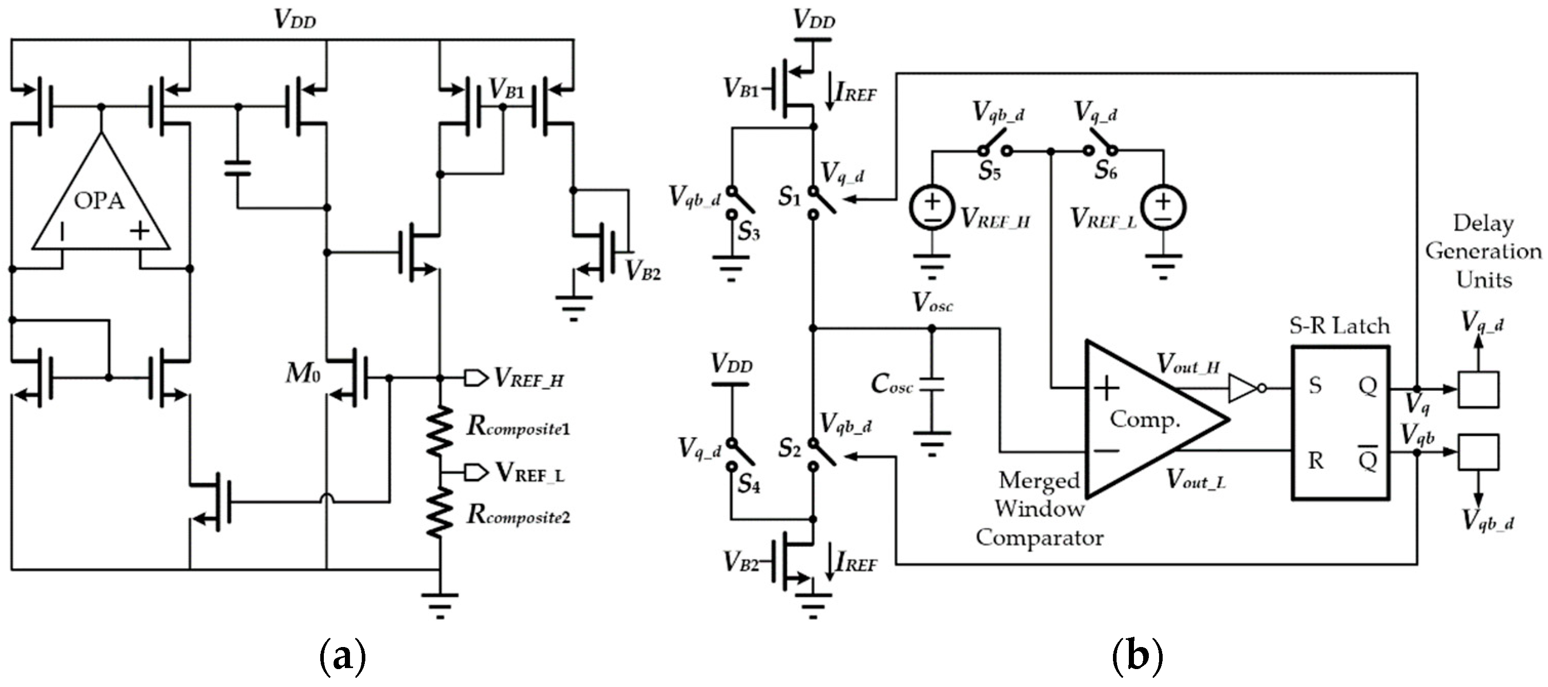
3.1. Topology of the Relaxation Oscillator

The relaxation oscillator, which makes use of the reported topology [24], is depicted in Figure 5. The major difference is that of the design and implementation of the current reference IREF, while the lower supply current consumption is further addressed in the proposed work. The oscillator comprises a reference generator, two comparators (Comp. 1 and Comp. 2), an S-R latch, four switches, and two capacitors (C1 and C2). The reference generator generates a stable reference voltage (VREF) and a reference current (IREF), charging two capacitors with a constant current.
Note that the relaxation oscillator circuit starts when Q is logic low, and the voltages across two capacitors are initially zero. At the beginning, the outputs of two comparators are low, and C1 is charged by IREF. After the voltage (VC1) across C1 reaches VREF, the output of Comp.1 transits to high, which allows Q to become high and Q_bar to become low. Then C1 starts to discharge, while C2 is charged by IREF. The inputs of the SR latch are both low when IREF is charging C2, so that the outputs of the SR latch remain constant until the voltage (VC2) rises to VREF. At this juncture, Q transits to low, while Q_bar transits to high, allowing C1 to be charged again and C2 to discharge. The output Q of the SR latch will generate a rail-to-rail square wave with the desired frequency. As capacitors are charged by a constant current, the duration of the high level and low level of the square wave are dependent on the charging time of each capacitor; hence, the 50% duty cycle can be achieved by using two identical capacitors. The output frequency can be expressed as
f R O S C = I R E F 2 C V R E F
where fROSC is the output frequency, and C is the capacitance of C1 and C2. From (1), the accuracy of the output frequency is dependent on the accuracy of VREF and IREF. From the design considerations, the reference generator and the comparator are the key components in circuit design. Two nonideal effects exist in the relaxation oscillator circuit. They are the delay and offset of the comparator. Regarding the comparator’s delay, it is not critical because of the low frequency specification and the moderate precision requirement in its application. With a careful designing of the comparator, the temperature-dependent delay of the comparator can be minimized to cause less impact to the circuit, and ultimately, on the output frequency. Pertaining to the comparator’s offset, it is also addressed in the design phase with an appropriate choice of critical device sizes so that the offset effect to the circuit is acceptable, without significantly jeopardizing the oscillator’s performance.

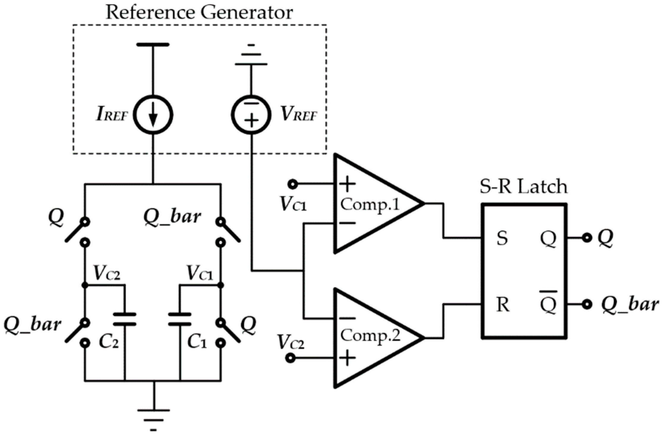
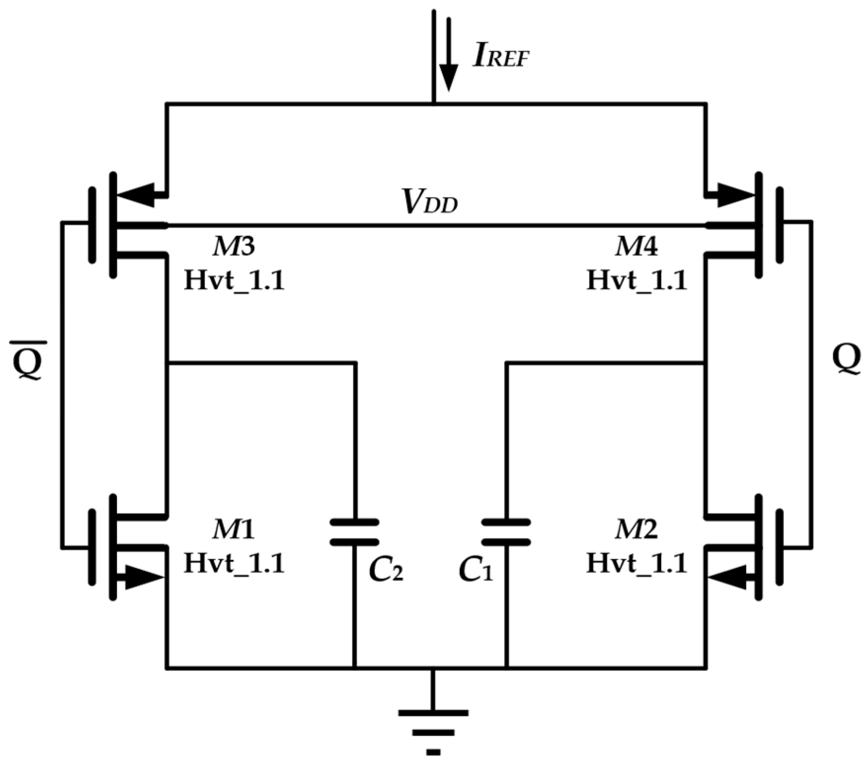
3.2. Reference Generator
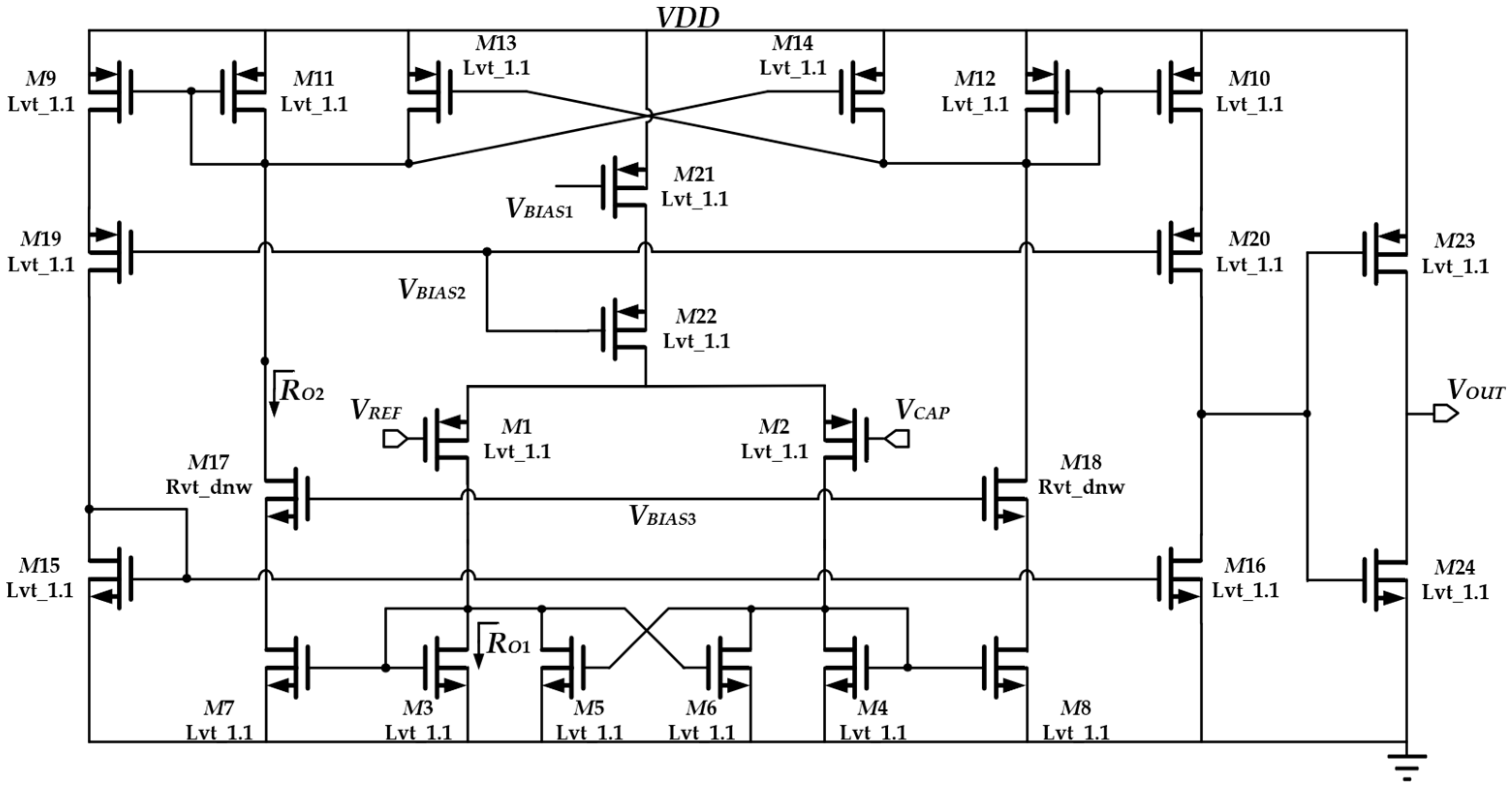
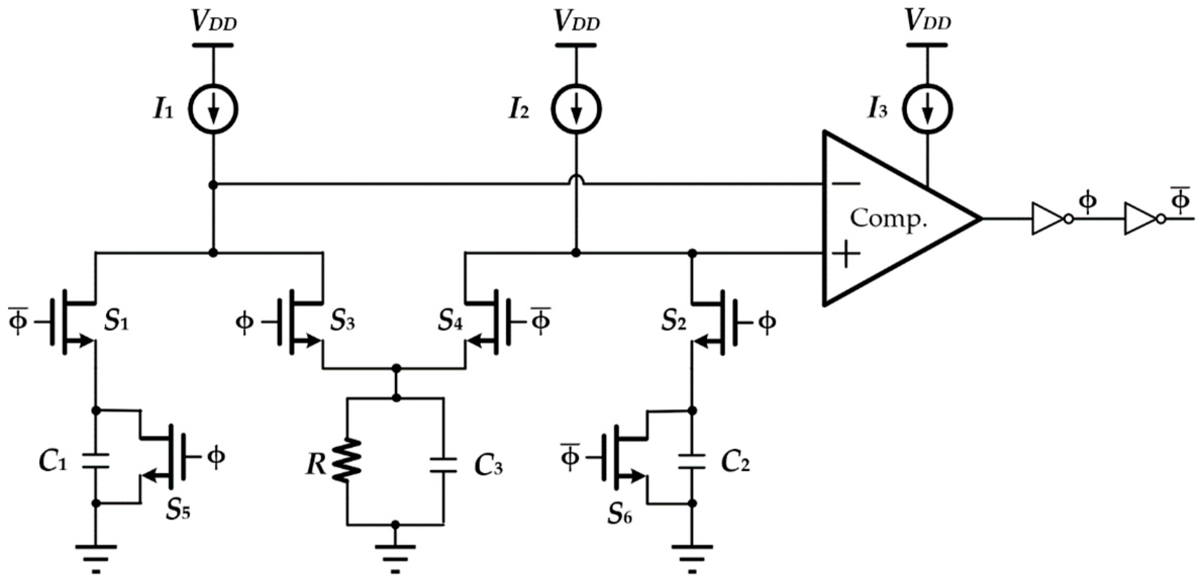
The reference generator, which provides both the reference voltage (VREF) and the reference current (IREF), is depicted in Figure 6. The reference voltage generator is based on the two-transistor topology [25] and the cascode current mirror. This is achieved by employing voltage-to-current and current-to-voltage conversions to produce VREF. This is then followed by another voltage-to-current converter with a composite resistor [26] and VREF to generate the reference current IREF.
Regarding the reference voltage generator, M1, M2, M3, and M4 work in the weak inversion region, where M1 and M3 are identically designed native transistors with a negative threshold voltage, whereas M2 and M4 are identical standard transistors. It is given that, for a sub-threshold biased MOSFET, its drain current is
I s u b = μ C O X ( η 1 ) V T 2 W L exp ( V G S V T H η V T ) [ 1 exp ( V D S V T ) ]
where μ is the carrier mobility, Cox is the gate-oxide capacitance, η is the subthreshold slope factor, VT is the thermal voltage, W is transistor’s channel width, L is transistor’s channel length, VGS is the gate-to-source voltage, VTH is the threshold voltage, and VDS is the drain-to-source voltage. When VDS is larger than 100 mV (4 VT), the effect of VDS on Isub is negligible; hence, the current Isub can be approximated as
I s u b μ C O X ( η 1 ) V T 2 W L exp ( V G S V T H η V T )
Since the currents in M1 and M2 are the same, we can obtain
I s u b = μ 1 C O X 1 ( η 1 1 ) V T 2 W 1 L 1 exp ( V G S 1 V T H 1 η 1 V T )   = μ 2 C O X 2 ( η 2 1 ) V T 2 W 2 L 2 exp ( V G S 2 V T H 2 η 2 V T )
The current of M1 and M2 is the same as that of M3 and M4 due to the identical current copying action in the cascode current mirror M5M8. Hence, the VGS of M2 is identical to that of M4, which is the VREF. When the gates of M1 and M3 are connected to a ground, it suggests that the VGS of M1 and M3 are identical negative reference voltages. Thus, VREF can be obtained as
V R E F = V G S 1 = V G S 2 = η 1 η 2 η 1 + η 2 ( V T H 2 V T H 1 ) + η 1 η 2 η 1 + η 2 V T ln ( μ 1 C O X 1 W 1 L 2 μ 2 C O X 2 W 2 L 1 )
In this design, the first-order temperature effect on VTH is given as [7]
V T H = V T H 0 κ T
where VTH0 is the threshold voltage at room temperature (300 K), and κ is the temperature coefficient of the threshold voltage. Therefore, the T.C. of VREF is as follows:
T C V R E F = 1 V R E F V R E F T = ( κ 1 κ 2 ) + k q ln ( μ 1 C O X 1 W 1 L 2 μ 2 C O X 2 W 2 L 1 ) ( V T H 20 V T H 10 ) + ( κ 1 κ 2 ) T + k q T ln ( μ 1 C O X 1 W 1 L 2 μ 2 C O X 2 W 2 L 1 )
where k is the Boltzman constant, and q is the electronic charge. In (7), the temperature effect on μ is ignored. By selecting appropriate aspect ratios of M1 and M2, while M3 and M4 remain the same size as M1 and M2, respectively, the temperature compensation can be achieved to permit VREF in the first-order temperature compensation. Finally, it yields
V R E F = η 1 η 2 η 1 + η 2 ( V T H 20 V T H 10 )
In addition, the VREF has a good power supply rejection (PSR) at low frequency. Since the effect of ΔVDD on the flowing currents, M2 and M4 are negligible, as long as their VDS values are larger than 100mV, while the transistors have a long channel length to reduce the drain-induced barrier lowering (DIBL) effect on VTH1~VTH4. Besides, the negative feedback formed by M3, M4, and M9 can further stabilize VREF.
For the reference current, it is produced by VREF driving a temperature-compensated composite resistor (Rs). Of particular note, Rs comprises the series connection of an n-poly resistor (Rn) and a p-poly resistor (Rp), where Rn is PTAT and Rp is CTAT. The T.C. of Rp, Rn, and Rs are given as follows:
T C R p = 1 R p R p T
T C R n = 1 R p R n T
T C R s = 1 R p + R n ( R p + R n ) T
Substituting (9) and (10) into (11), TCRs can be rewritten as
T C R s = R p R p + R n T C R p + R n R p + R n T C R n
where TCRp is negative and TCRn is positive. Thus, TCRs can be made zero when choosing Rp/Rn equal to |TCn/TCp|. This indicates that Rs can be independent of the first-order temperature effect. Therefore, the temperature-insensitive reference current (IREF) can be obtained with the temperature-insensitive voltage and the composite resistor.
I R E F = V R E F R s = η 1 η 2 ( V T H 20 V T H 10 ) ( η 1 + η 2 ) ( R p + R n )
Moreover, since Rs is independent of VDD, VREF is insensitive to the change in VDD. As a result, IREF is also insensitive to the supply variations.
As seen in Figure 6, the capacitor C1 is used as a frequency compensation for the negative feedback loop which is formed by M3, M4, and M9. In addition, the capacitor C2 is used to stabilize VREF when the switches in Figure 4 are turned on and off. This is because the voltage change will be coupled to the gate of M9 by the parasitic capacitors. The current mirror pairs M5M8 and M10M13 have a long channel length to reduce the current mismatch.
The 1.1 V supply voltage of this reference generator can ensure that all transistors still work in the proper region when there is a 10% supply voltage drop, but if the supply continuously decreases below 1 V, there will not be adequate VDS headroom for the current mirror pair in Figure 6 at the SS corner under a low temperature, due to the increase in VTH.
Finally, the size of each component pertaining to Figure 5 in the reference generator is listed in Table 1.

3.3. Comparator

The comparator in Figure 7 shows an OTA topology using dual cross-coupled load pairs and a cascode arrangement to boost the overall gain. The front differential stage, which makes use of the cross-coupled load pairs, M3M6 and M13M16, is used to produce gain enhancement as well as to reduce the delay in the comparator, the outputs of which are followed by the current mirror high-gain stage consisting of M7M12 and M15M20. Finally, the CMOS inverter, formed by M23 and M24, aims to sharpen the output square waveform and provide the driving capability of the comparator.
Considering the cross-coupled pairs M3M6, the aspect ratio of M3 is larger than that of M5. In small-signal analysis, the output impedance is obtained as
R O 1 = r O 3 + r O 5 ( g m 3 g m 5 ) ( r O 3 + r O 5 ) + 1 1 g m 3 g m 5
where gmi is the respective transistor’s transconductance and rOi is the respective transistor’s output resistance, with i = 3 or 5. From (14), RO1 is increased from 1/gm3 to 1/(gm3gm5) to increase the voltage gain because of the positive feedback allowing M5 to behave as a negative resistance. When there is a voltage change on the drain of M3, the positive feedback introduced by M5 can accelerate this change, causing faster output response to reduce the delay in the comparator.
The four cascode transistors M17M20 are used to reduce the effect of supply variation ΔVDD on the delay in the comparator. For M7 and M17 in small-signal analysis, the change in VDS7 caused by ΔVDD can be approximated as [27]
Δ V D S 7 Δ V D D g m 17 r O 17
As interpreted from (15), it indicates that the change in VDS on M7M10 can be ignored when VDD varies. This means the current change in each branch caused by channel length modulation and DIBL can be minimized with cascode transistors. Moreover, the bias current for the comparator is directly copied from IREF, with the cascode current mirror in different ratios. This avoids the need for an extra bias branch, which would cause an increase in supply current consumption.
In fact, when the constant bias current is applied to the comparator, the delay in the comparator is reduced with an increasing temperature. From (3) and (6), the VGS of the MOS transistor working under weak inversion is expressed as
V G S = η V T ln [ I s u b μ C O X ( η 1 ) V T 2 W L ] + V T H 0 κ T
It can be observed that the VGS exhibits CTAT behavior. M3 is in the diode connection, meaning that VDS3 is equal to VGS3. When the temperature increases, VDS3 (or VGS3) in the diode-connected topology is significantly reduced with respect to VDS7. Thus, the mismatch between the drain-to-source voltage of the transistors can lead to a rising current to allow for the delay in the comparator to decrease from 285.3 ns to 278.8 ns as the temperature increases, as shown in Figure 8. This feature is particularly useful for the delay compensation arising from the observation of the increase in delay through the leakage current of the switches, as depicted in Figure 4. As a result, the thermal stability of the oscillator circuit is enhanced. This will be further discussed in the next subsection. Of particularly note, the leakage current in the advanced technology node can be a serious issue.
Since offset is critical in the comparator design, the Monte Carlo simulation, with 400 samples for the offset evaluation, is shown in Figure 9. This result indicates that the mean offset of the comparator is 0.37 mV, and its standard derivation is 5.63 mV. As observed, the offset is minimized by sizing the input transistor pair and the cross-coupled pairs with a long channel length (L > 4Lmin). Although the parasitic capacitors in the large-size transistors will enlarge the response time, the delay, which is around 0.28 µs, including the hysteresis, contributes 3.6% of the oscillation period. Therefore, it is considered acceptable, with a low output frequency and a moderate precision requirement. Based on the result, the comparator offset cancellation scheme is not implemented in this work. The sizes of each component pertaining to the comparator in Figure 6 are given in Table 2.

3.4. Leakage Current in Switches and Delay Compensation

The four switches controlling the charging and discharging actions, as depicted in Figure 5, are arranged in the inverted style, as shown in Figure 10.
Since IREF is quite small, the leakage currents in the advanced technology node, flowing through the switch transistors, can be significant when charging C1 and C2. With the increase in temperature, the delay caused by the transistor switches is increased from 1.9 ns to 9.8 ns, as shown in Figure 11, and this effect is particularly pronounced. Therefore, this will cause the reduction in the output frequency. Thus, according to the reverse short-channel effect, high threshold-voltage transistors with the smallest channel length can be used as switches. This is also in conjunction with introducing the body effect in pmos to maximize the threshold voltage. Finally, the leakage current effect can be reduced by introducing the CTAT delay, as discussed in Section 3.3, such that the output frequency can be kept constant. The size of each transistor and capacitor shown in Figure 10 are given in Table 3.

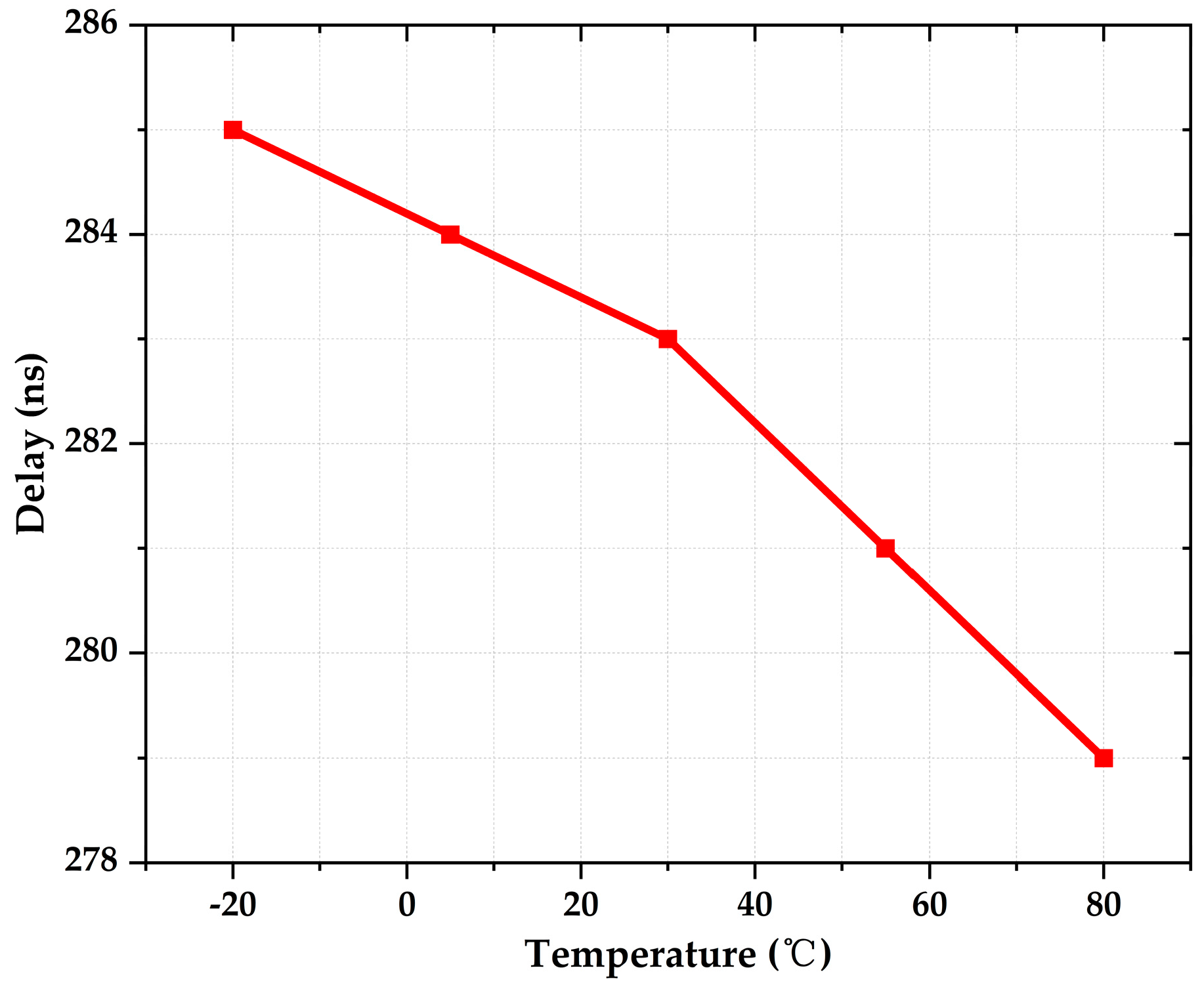
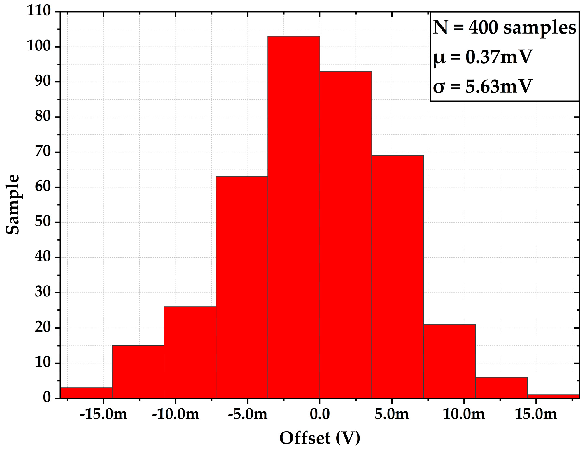
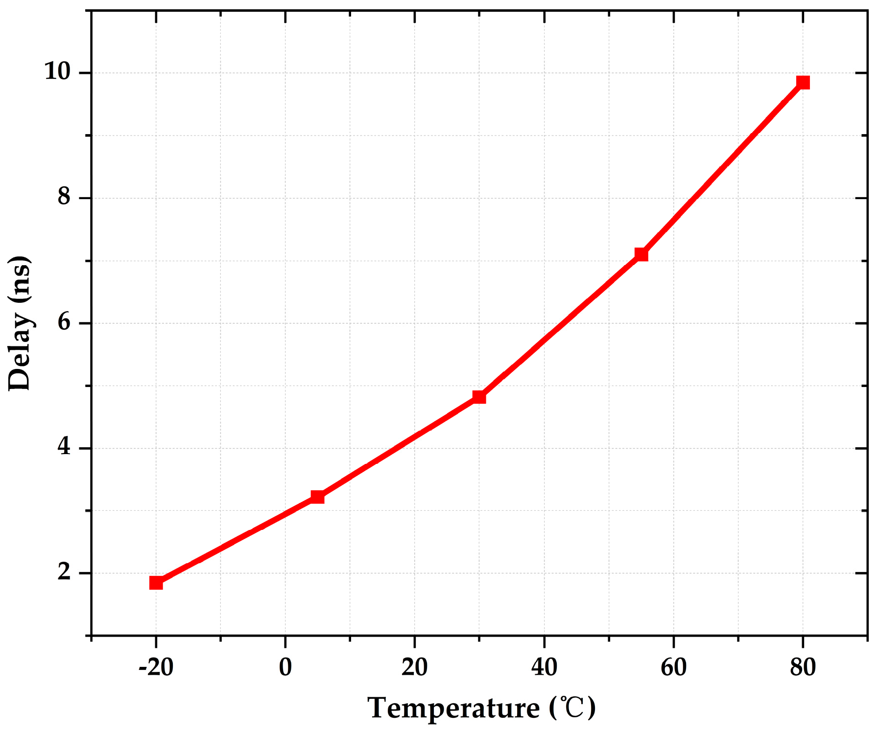
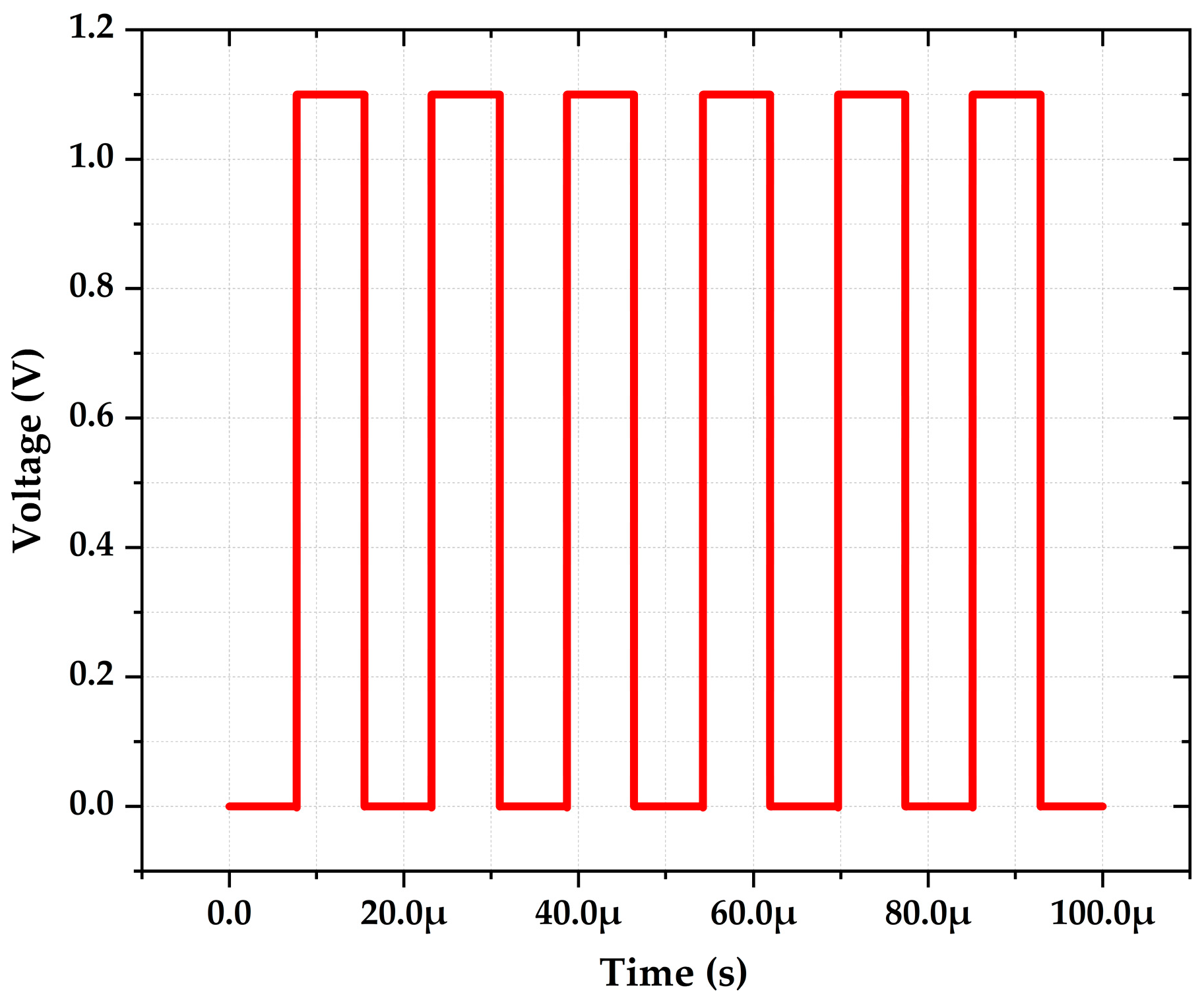
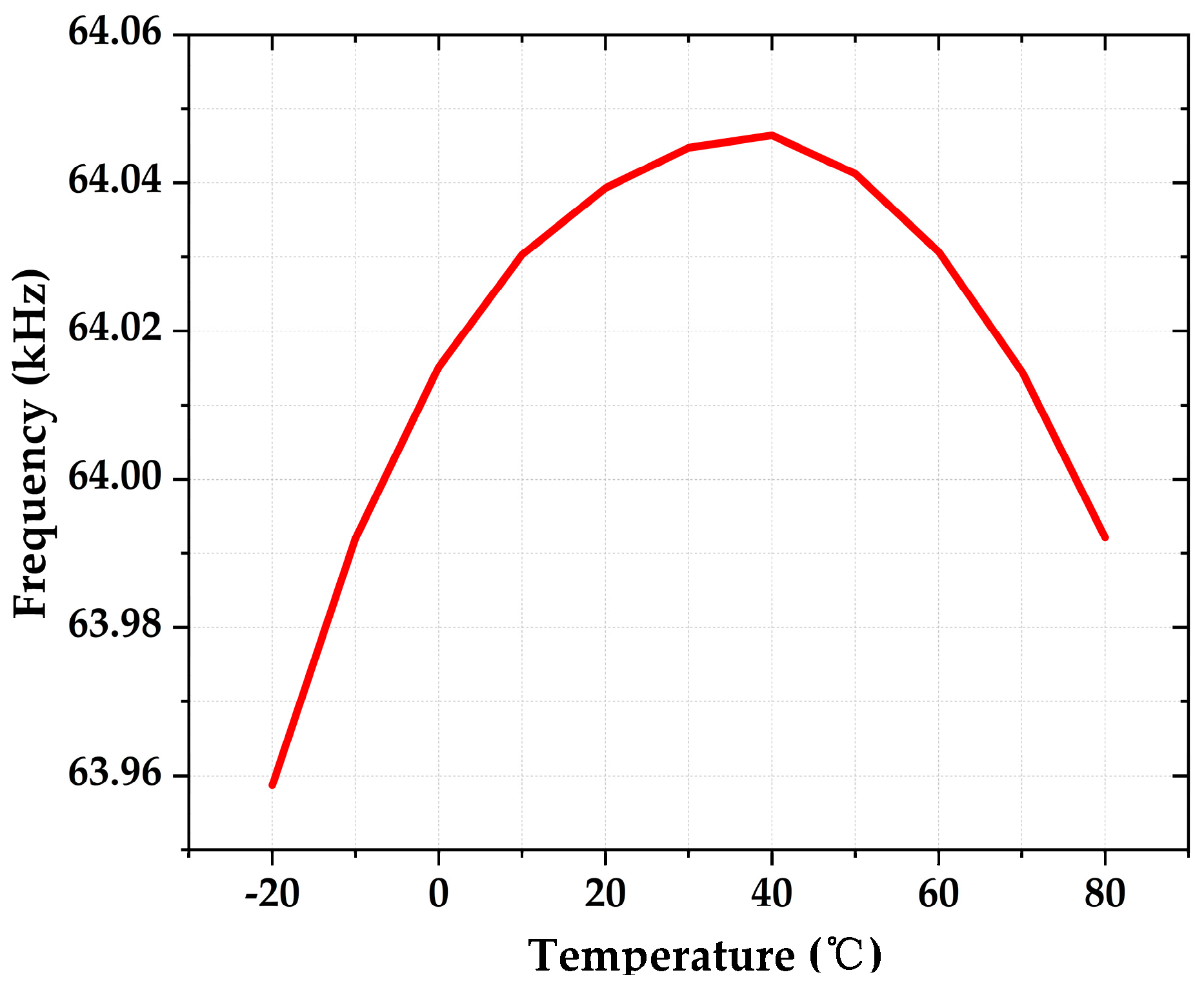
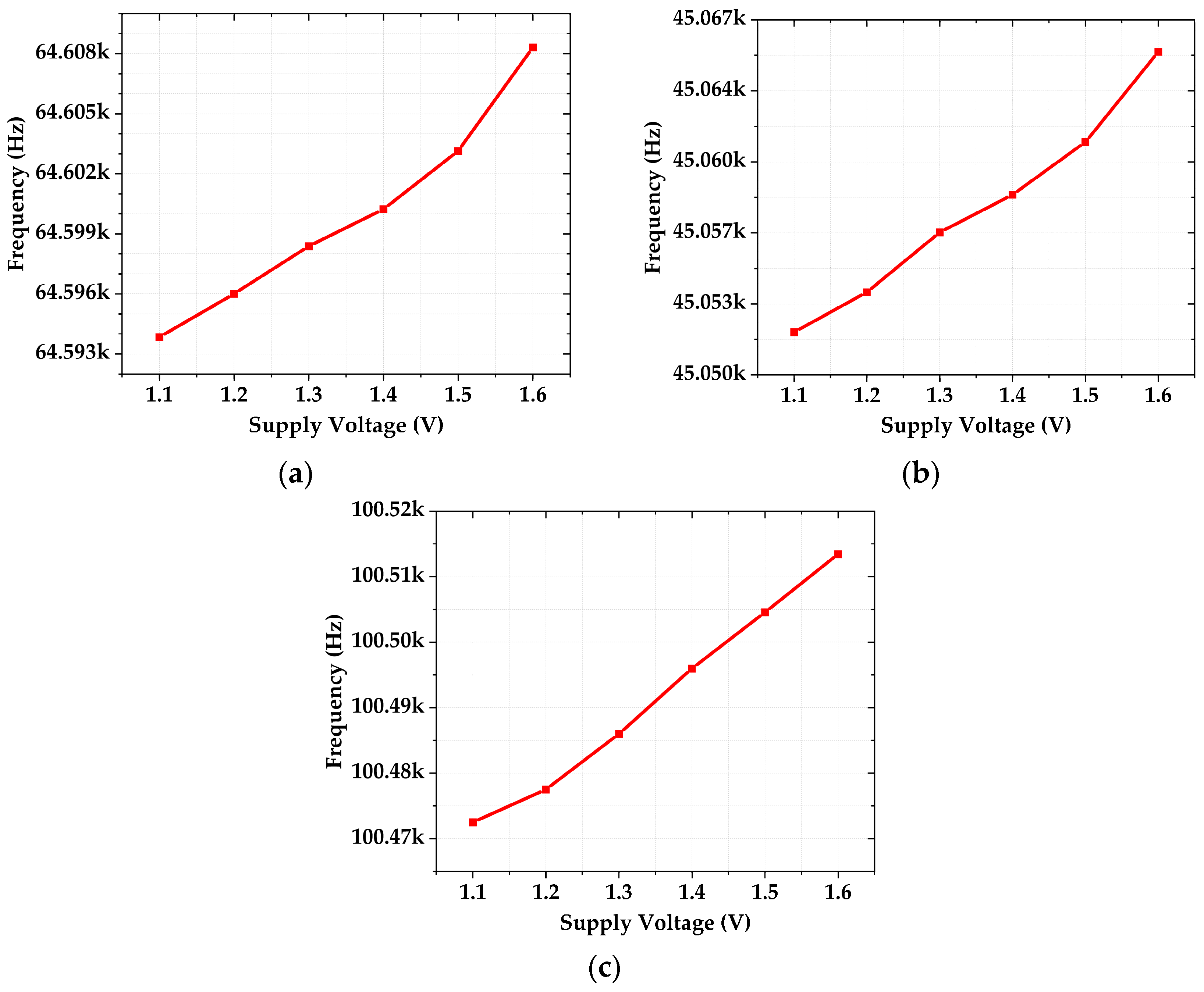
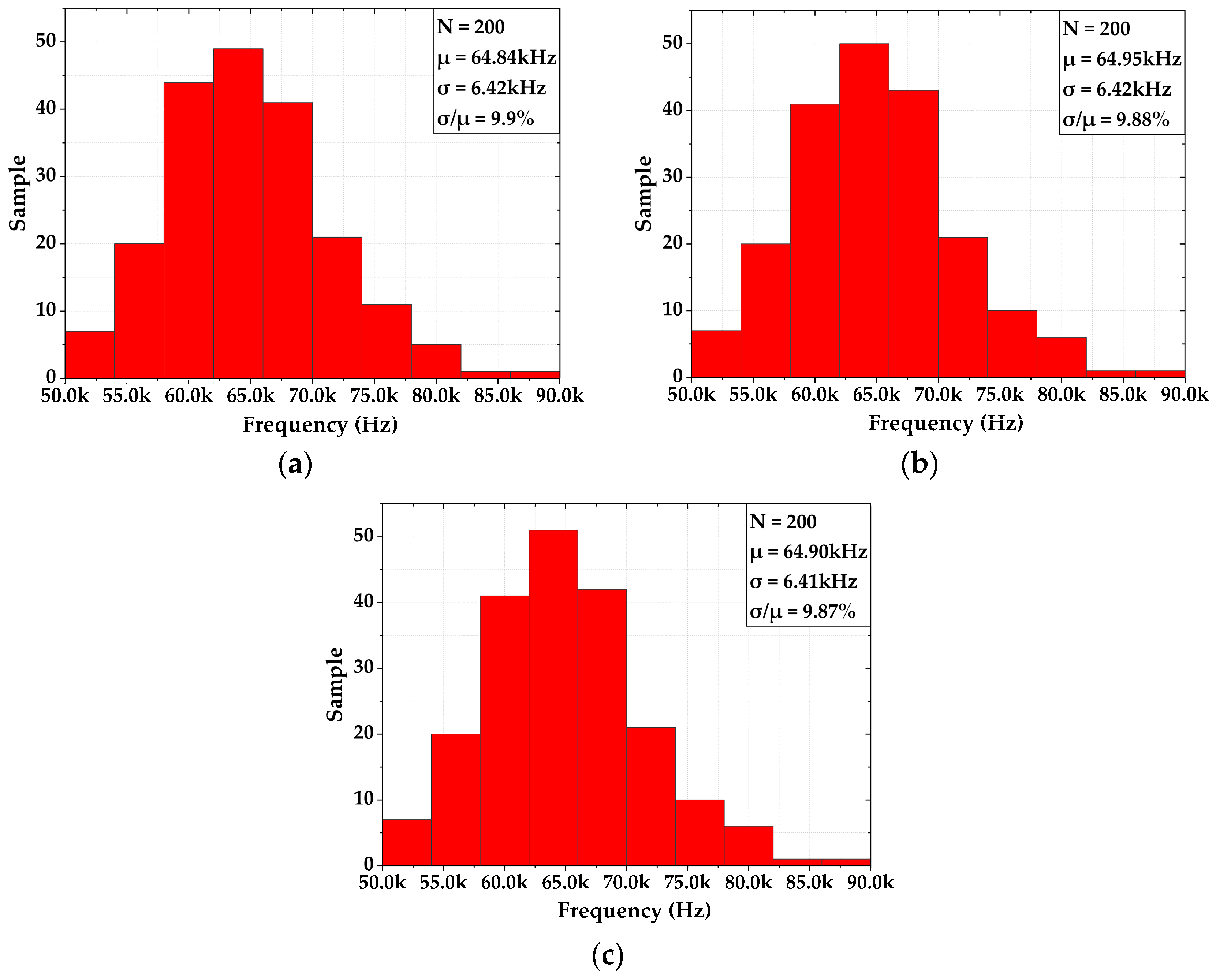
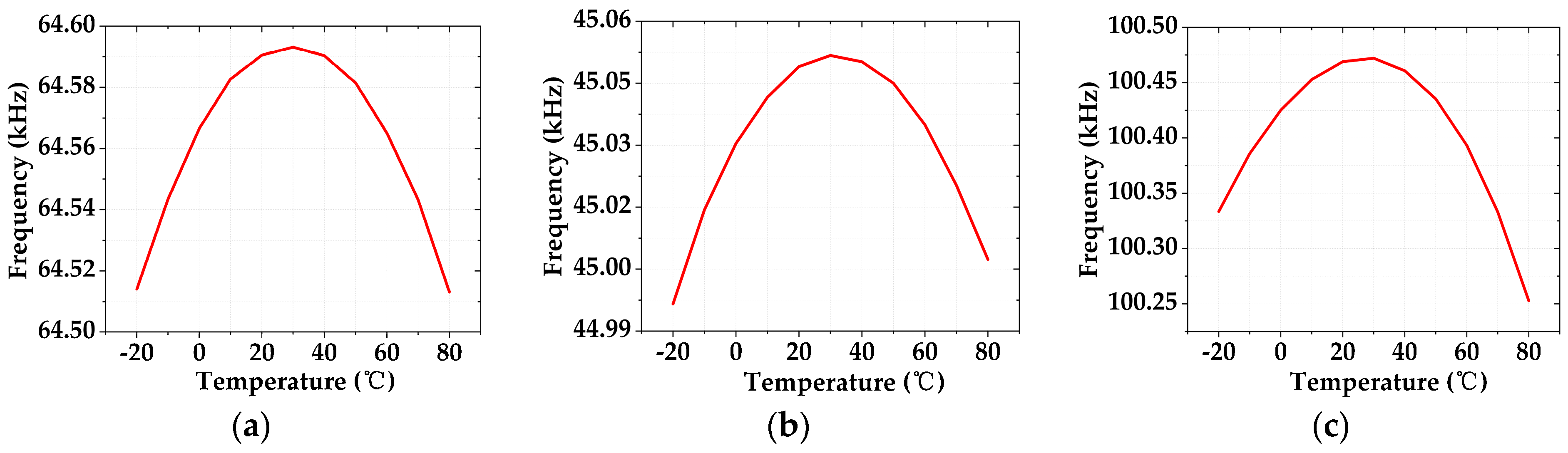
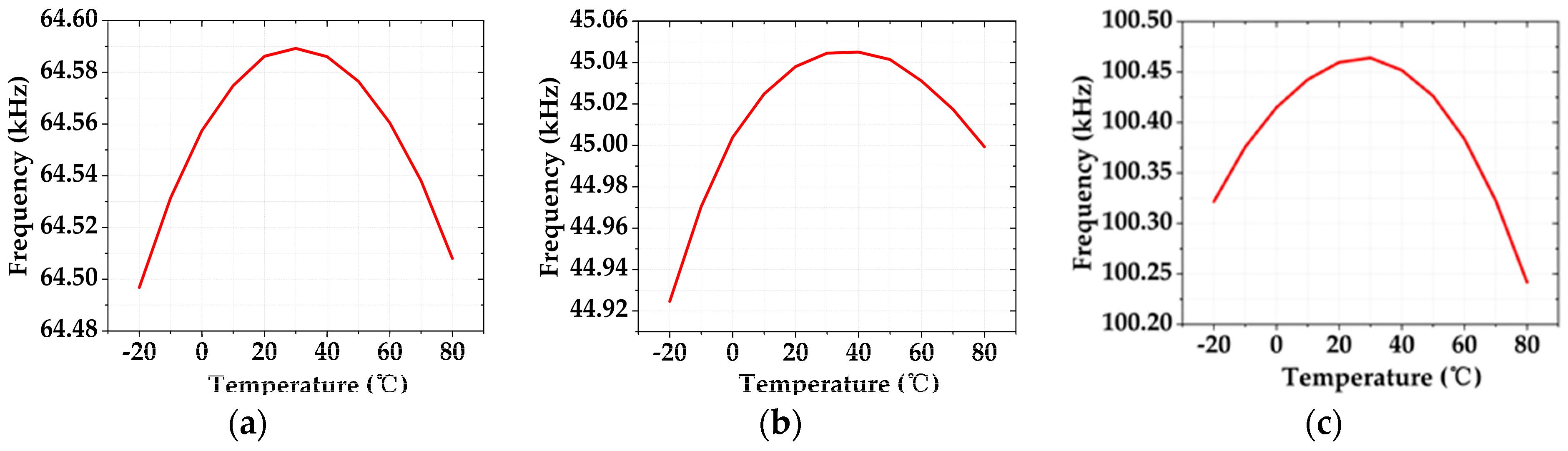
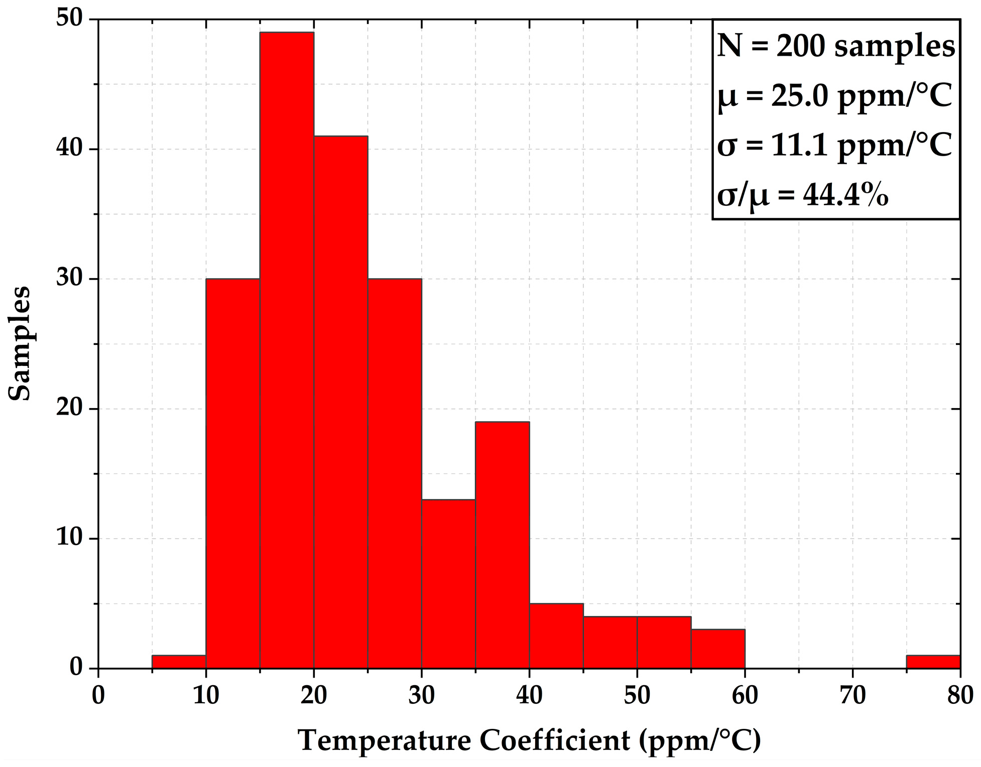
4. Results and Discussions

The proposed ROSC, with leakage current compensation, is simulated using TSMC-40 nm CMOS process technology. The output frequency is 64.59 kHz at VDD = 1.1 V under room temperature, and the transient simulation result of the output signal is depicted in Figure 12. All analog-biased transistors in the proposed ROSC work in the subthreshold region, the bias current of the comparators can be made small for low frequency design, and the current derives from the dedicated IREF instead of from the addition of an extra current source. This permits the current consumption of 552 nA at room temperature in a typical corner. However, there is always a performance tradeoff between IREF and low current consumption.
Figure 13 and Figure 14 illustrate the respective simulation results of the output frequency against the temperature variation from −20 °C to 80 °C at different supply voltages and process corners. The T.C. of the output frequency of the proposed ROSC is obtained as 12.4 ppm/°C, 13.3 ppm/°C, and 21.8 ppm/°C at the TT corner, SS corner, and FF corner, respectively, at a 1.1 V supply. Regarding the 1 V supply, the obtained T.C. is 14.3 ppm/°C, 26.7 ppm/°C, and 22.2 ppm/°C, respectively. Of particular note, the T.C. is observed with some degradation at the 1 V supply with respect to that of the 1.1 V supply at the SS corner. This is mainly because the transistors in the reference generator are stressed under limited VDS. Therefore, the proposed ROSC can still work properly when the supply is slightly lower than 1.1 V. Considering the operation margin, 1.1 V is regarded as the minimum supply voltage for the oscillator. Regarding the low T.C. values achieved by the ROSC with respect to those of prior-art works, the T.C. improvement is attributed to the compensation for the delay drift resulting from temperature, as seen in Figure 8 and Figure 11. By calculation, without the delay compensation, this T.C. will increase to about 19.1 ppm/°C.
Considering the parasitic effect arising from the layout issues, some model capacitors ranging from a few tens to one hundred fF are intentionally added to the critical points in each comparator, reference generator, and SR latch. The comparator displays relatively higher sensitivity due to the low bias current, while there is no significant effect from other nodes. Figure 15 shows the simulated temperature characteristic of output frequency with intentionally added parasitic capacitors in the design under the TT corner. Of particular note, the estimated capacitance from the routing for each comparator is around 18fF. Therefore, the total capacitance of several model capacitors being added in each comparator is modeled as 20 fF. The output frequency changes from 64.59 kHz to 64.04 kHz, and the T.C. is degraded from 12.4 ppm/°C to 13.7 ppm/°C. This confirms that the potential parasitic effect arising from the layout made no significant impact on the current simulation results, without incorporating layout due to the low-frequency design. Additionally, the silicon area of this design is approximated as about 4x the total active area of the components. This yields about 0.0234 mm2, or 153 µm × 153 µm.
The T.C. results of Monte Carlo simulation used to verify the impact of mismatch and process variations are shown in Figure 16. There are 200 samples simulated, and each sample is simulated with 11 temperature points, from −20 °C to 80 °C, resulting in 2200 points in total. The T.C. varies from 9.35 ppm/°C to 77.13 ppm/°C, with an average value of 25 ppm/°C and a standard deviation of 11.1 ppm/°C, where 75% of the samples present a T.C. smaller than 30 ppm/°C. This confirms that the output frequency of the proposed ROSC exhibits good stability under temperature change.
The supply dependence of the output frequency is depicted in Figure 17. The line sensitivity of the output frequency achieves 0.045%/V, 0.059%/V, and 0.081%/V at the TT corner, SS corner, and FF corner, respectively, from a 1.1 V to 1.6 V supply, which is attributed to VREF with good PSR at low frequency and the cascode transistors shielding the variation of supply in the comparators to stabilize the response time.
The Monte Carlo simulation of the output frequency, with process variation and mismatch at different temperatures, is shown in Figure 18. The average values of the output frequency under different temperatures remain almost the same: 64.84 kHz, 64.95 kHz, and 64.9 kHz, with the standard deviation of 6.42 kHz, 6.42 kHz, and 6.41 kHz at −20 °C, 30 °C, and 80 °C, respectively. This yields the average process sensitivity (σ/µ) of 9.88%. The output frequency is eventually dependent on the value of the composite resistor Rs in Figure 6 and the capacitors C1 and C2 in Figure 10. The process variation displays the moderate value, which is targeted for moderate precision applications. However, to cater to a precision design, this can be achieved by trimming the passive MoM capacitors C1 and C2, which are less affected by temperature.
The performance of the proposed ROSC is compared to that of the previously reported representative works using advanced process technology nodes, as shown in Table 4, and with longer channel length technology nodes, as shown in Table 5. It can be seen that the proposed relaxation oscillator, with the dynamic current consumption of 552 nA at a 1.1 V supply voltage, exhibits the best T.C. for one sample. The same goes for the Monte Carlo 200-sample result, with process variation and mismatch. Regarding line sensitivity, the proposed work a displays lower value due to the use of the cascode current mirror plus the two-transistor-based voltage reference topology, which has the feature of small line sensitivity.
The process sensitivity of the output frequency is comparable and can be improved by trimming the two capacitors. To evaluate the stability of the output frequency, with both temperature and supply variations, a figure-of-merit (FoM), including the temperature coefficient and the line sensitivity [9], is defined as
F o M = T . C . × 100   ° C + L i n e . S e n s . × 10 % V D D min
where T.C. is the one sample value at the typical corner. The FoM of the proposed ROSC is 0.129%, which displays the best result when compared to the prior-art works shown in Table 4. Therefore, the proposed design can offer a stable frequency while providing a good tradeoff between stability and power consumption. Finally, in view of the larger leakage current, as well as the lower transistor intrinsic gain in this 40 nm technology with respect to those of technology nodes having a longer channel length, the frequency stability of the proposed work, as shown in Table 5, also shows excellent FoM. This demonstrates the usefulness of the circuit.

5. Conclusions

This paper presents a 40 nm CMOS relaxation oscillator with low-current consumption. It features simple topology that comprises a two-transistor-based voltage reference generator and a simple current reference generator with a temperature-compensated composite resistor. Moreover, the comparators are designed with a CTAT delay to counteract the PTAT delay contributed by the effect of the leakage current in switches, thus improving the thermal stability of the output frequency.
The simulation results confirmed that the proposed ROSC displayed excellent output frequency stability against the changes in temperature and supply voltage. Therefore, the proposed work is suitable for low-power applications that require an oscillator with a stable frequency and moderate precision.

Author Contributions

Conceptualization, Y.L. and P.K.C.; methodology, Y.L. and P.K.C.; software, Y.L.; validation, Y.L. and P.K.C.; formal analysis, Y.L. and P.K.C.; investigation, Y.L. and P.K.C.; resources, P.K.C.; data curation, Y.L.; writing—original draft preparation, Y.L.; writing—review and editing, P.K.C.; visualization, Y.L.; supervision, P.K.C.; project administration, P.K.C. All authors have read and agreed to the published version of the manuscript.

Funding

This research received no external funding.

Data Availability Statement

The study did not report any data.

Conflicts of Interest

The authors declare no conflict of interest.

References

  1. Tsubaki, K.; Hirose, T.; Kuroki, N.; Numa, M. A 32.55-kHz, 472-nW, 120ppm/°C, fully on-chip, variation tolerant CMOS relaxation oscillator for a real-time clock application. In Proceedings of the 2013 Proceedings of the ESSCIRC, Bucharest, Romania, 16–20 September 2013; pp. 315–318. [Google Scholar]
  2. Wang, J.; Goh, W.L. A 13.5-MHz relaxation oscillator with ±0.5% temperature stability for RFID application. In Proceedings of the 2016 IEEE International Symposium on Circuits and Systems, Montreal, QC, Canada, 22–25 May 2016; pp. 2431–2434. [Google Scholar]
  3. Cannillo, F.; Toumazou, C.; Lande, T.S. Nanopower subthreshold MCML in submicrometer CMOS technology. IEEE Trans. Circuits Syst. I Regul. Pap. 2009, 56, 1598–1611. [Google Scholar] [CrossRef]
  4. Zhang, S.; Li, A.; Han, Y.; Jie, L.; Han, X.; Cheung, R.C. Temperature compensation technique for ring oscillators with tail current. Electron. Lett. 2016, 52, 1108–1110. [Google Scholar] [CrossRef]
  5. Zhang, X.; Apsel, A.B. A low-power, process-and-temperature-compensated ring oscillator with addition-based current source. IEEE Trans. Circuits Syst. I Regul. Pap. 2010, 58, 868–878. [Google Scholar] [CrossRef]
  6. Ballo, A.; Pennisi, S.; Scotti, G.; Venezia, C. A 0.5 V Sub-Threshold CMOS Current-Controlled Ring Oscillator for IoT and Implantable Devices. J. Low Power Electron. 2022, 12, 16. [Google Scholar] [CrossRef]
  7. Cimbili, B.; Wang, D.; Zhang, R.C.; Tan, X.L.; Chan, P.K. A PVT-tolerant relaxation oscillator in 65nm CMOS. In Proceedings of the 2016 IEEE Region 10 Conference, Singapore, 22–25 November 2016; pp. 2315–2318. [Google Scholar]
  8. Ma, L.; Koay, K.C.; Chan, P.K. A merged window comparator based relaxation oscillator with low temperature coefficient. In Proceedings of the 2017 IEEE International Symposium on Circuits and Systems, Baltimore, MD, USA, 28–31 May 2017; pp. 1–4. [Google Scholar]
  9. Medeiros, W.T.; Klimach, H.; Bampi, S. A 40 nW 32.7 kHz CMOS Relaxation Oscillator with Comparator Offset Cancellation for Ultra-Low Power applications. In Proceedings of the 2020 IEEE 11th Latin American Symposium on Circuits & Systems, San Jose, Costa Rica, 25–28 February 2020; pp. 1–4. [Google Scholar]
  10. Hsiao, K.J. A 32.4 ppm/°C 3.2-1.6 V self-chopped relaxation oscillator with adaptive supply generation. In Proceedings of the 2012 Symposium on VLSI Circuits, Honolulu, HI, USA, 13–15 June 2012; pp. 14–15. [Google Scholar]
  11. Xu, L.; Onabajo, M. A low-power temperature-compensated relaxation oscillator for built-in test signal generation. In Proceedings of the 2015 IEEE 58th International Midwest Symposium on Circuits and Systems, Fort Collins, CO, USA, 2–5 August 2015; pp. 1–4. [Google Scholar]
  12. Chan, P.K.; Zhang, H.L. A switched-capacitor interface circuit for integrated sensor applications. In Proceedings of the 2001 IEEE International Symposium on Circuits and Systems, Sydney, NSW, Australia, 6–9 May 2001; pp. 372–375. [Google Scholar]
  13. Ye, S.Q.; Chan, P.K. A low-power switched-capacitor humidity sensor interface. In Proceedings of the 2010 IEEE Asia Pacific Conference on Circuits and Systems, Kuala Lumpur, Malaysia, 6–9 December 2010; pp. 1039–1042. [Google Scholar]
  14. Ong, G.T.; Chan, P.K. A Power-Aware Chopper-Stabilized Instrumentation Amplifier for Resistive Wheatstone Bridge Sensors. IEEE Trans. Instrum. Meas. 2014, 63, 2253–2263. [Google Scholar] [CrossRef]
  15. Chan, P.K.; Ng, K.A.; Zhang, X.L. A CMOS chopper-stabilized differential difference amplifier for biomedical integrated circuits. In Proceedings of the 2004 47th Midwest Symposium on Circuits and Systems, Hiroshima, Japan, 25–28 July 2004; pp. 3–33. [Google Scholar]
  16. Savanth, A.; Weddell, A.S.; Myers, J.; Flynn, D.; Al-Hashimi, B.M. A Sub-nW/kHz Relaxation Oscillator with Ratioed Reference and Sub-Clock Power Gated Comparator. IEEE J. Solid-State Circuits 2019, 54, 3097–3106. [Google Scholar] [CrossRef]
  17. Tsai, Y.-K.; Lu, L.-H. A 51.3-MHz 21.8-ppm/°C CMOS Relaxation Oscillator with Temperature Compensation. IEEE Trans. Circuits Syst. II Express Briefs 2017, 64, 490–494. [Google Scholar] [CrossRef]
  18. Ji, Y.; Liao, J.; Arjmandpour, S.; Novello, A.; Sim, J.-Y.; Jang, T. A Second-Order Temperature-Compensated On-Chip R-RC Oscillator Achieving 7.93 ppm/°C and 3.3pJ/Hz in −40 °C to 125 °C Temperature Range. In Proceedings of the 2022 IEEE International Solid-State Circuits Conference, San Francisco, CA, USA, 20–26 February 2022; pp. 1–3. [Google Scholar]
  19. Asano, H.; Hirose, T.; Ozaki, T.; Kuroki, N.; Numa, M. An area-efficient, 0.022-mm2, fully integrated resistor-less relaxation oscillator for ultra-low power real-time clock applications. In Proceedings of the 2017 IEEE International Symposium on Circuits and Systems, Baltimore, MD, USA, 28–31 May 2017; pp. 1–4. [Google Scholar]
  20. Paidimarri, A.; Griffith, D.; Wang, A.; Chandrakasan, A.P.; Burra, G. A 120 nW 18.5 kHz RC oscillator with comparator offset cancellation for ±0.25% temperature stability. In Proceedings of the 2013 IEEE International Solid-State Circuits Conference Digest of Technical Papers, San Francisco, CA, USA, 17–21 February 2013; pp. 184–185. [Google Scholar]
  21. Lee, J.; Cho, S. A 210 nW 29.3 ppm/°C 0.7 V voltage reference with a temperature range of −50 to 130 °C in 0.13 µm CMOS. In Proceedings of the 2011 Symposium on VLSI Circuits-Digest of Technical Papers, Kyoto, Japan, 15–17 June 2011; pp. 278–279. [Google Scholar]
  22. Allen, P.E.; Holberg, D.R. CMOS Analog Circuit Design; Oxford University Press: Oxford, UK, 2002. [Google Scholar]
  23. Denier, U. Analysis and design of an ultralow-power CMOS relaxation oscillator. IEEE Trans. Circuits Syst. I Regul. Pap. 2010, 57, 1973–1982. [Google Scholar] [CrossRef]
  24. Flynn, M.P.; Lidholm, S.U. A 1.2-mum CMOS current-controlled oscillator. IEEE J. Solid-State Circuits 1992, 27, 982–987. [Google Scholar] [CrossRef]
  25. Seok, M.; Kim, G.; Blaauw, D.; Sylvester, D. A portable 2-transistor picowatt temperature-compensated voltage reference operating at 0.5 V. IEEE J. Solid-State Circuits 2012, 47, 2534–2545. [Google Scholar] [CrossRef]
  26. Gregoire, B.R.; Moon, U.K. Process-independent resistor temperature-coefficients using series/parallel and parallel/series composite resistors. In Proceedings of the 2007 IEEE International Symposium on Circuits and Systems, New Orleans, LA, USA, 27–30 May 2007; pp. 2826–2829. [Google Scholar]
  27. Razavi, B. Design of Analog CMOS Integrated Circuits; McGraw-Hill Education: New York, NY, USA, 2005. [Google Scholar]
  28. Chiang, Y.-H.; Liu, S.-I. Nanopower CMOS Relaxation Oscillators With Sub-100 ppm/°C Temperature Coefficient. IEEE Trans. Circuits Syst. II Express Briefs 2014, 61, 661–665. [Google Scholar]
  29. De Vita, G.; Marraccini, F.; Iannaccone, G. Low-Voltage Low-Power CMOS Oscillator with Low Temperature and Process Sensitivity. In Proceedings of the 2007 IEEE International Symposium on Circuits and Systems, New Orleans, LA, USA, 27–30 May 2007; pp. 2152–2155. [Google Scholar]
Figure 1. Tradeoff performance of reported relaxation oscillators: (a) T.C. versus power; (b) line sensitivity versus power.
Jlpea 13 00015 g001
Figure 2. A CMOS relaxation oscillator with a merged window comparator: (a) reference generator; (b) block diagram.
Jlpea 13 00015 g002
Figure 3. A Relaxation Oscillator with Ultra-Low Power Consumption.
Jlpea 13 00015 g003
Figure 4. A self-chopped relaxation oscillator with adaptive supply generation: (a) block diagram; (b) clock buffer.
Jlpea 13 00015 g004
Figure 5. Block diagram of relaxation oscillator.
Jlpea 13 00015 g005
Figure 6. Proposed reference voltage and reference current generator.
Jlpea 13 00015 g006
Figure 7. Proposed comparator.
Jlpea 13 00015 g007
Figure 8. Temperature characteristics of delay in comparators.
Jlpea 13 00015 g008
Figure 9. Monte Carlo simulation of the comparator’s offset.
Jlpea 13 00015 g009
Figure 10. Four transistor switches for charging and discharging the matched capacitor pair.
Jlpea 13 00015 g010
Figure 11. Temperature characteristics of the delay in transistor switches.
Jlpea 13 00015 g011
Figure 12. Output signal in time domain.
Jlpea 13 00015 g012
Figure 13. Temperature characteristic of output frequency at different process corners under the 1.1 V supply: (a) @TT corner; (b) @SS corner; (c) @FF corner.
Jlpea 13 00015 g013
Figure 14. Temperature characteristic of output frequency at different process corners under the 1 V supply: (a) @TT corner; (b) @SS corner; (c) @FF corner.
Jlpea 13 00015 g014
Figure 15. Temperature characteristic of output frequency with simulated parasitic capacitors at the TT corner.
Jlpea 13 00015 g015
Figure 16. Monte Carlo simulation of output frequency T.C.
Jlpea 13 00015 g016
Figure 17. Supply dependence of output frequency at different process corners: (a) @TT corner; (b) @SS corner; (c) @FF corner.
Jlpea 13 00015 g017
Figure 18. Monte Carlo simulation of output frequency: (a) @−20 °C; (b) @30 °C; (c) @80 °C.
Jlpea 13 00015 g018
Table 1. Size of components in the reference generation.
ComponentSizeComponentSize
M1,310/15 (µm/µm)M10,1228/12 (µm/µm)
M22.04/1 (µm/µm)M11,137/2 (µm/µm)
M42.05/1 (µm/µm)R1433.3 kΩ
M5,75/4 (µm/µm)R21.366 MΩ
M6,86/2 (µm/µm)C11.5 pF
M91.5/1 (µm/µm)C24 pF
Table 2. Size of the components in the comparator.
ComponentSizeComponentSize
M1,2 1/0.6 (µm/µm)M15,160.5/0.6 (µm/µm)
M3,4 1/1.2 (µm/µm)M17,180.3/0.3 (µm/µm)
M5,6 0.8/1.2 (µm/µm)M19,200.3/0.3 (µm/µm)
M7,8 0.5/0.6 (µm/µm)M2120/12 (µm/µm)
M9,10 0.5/0.6 (µm/µm)M225/2 (µm/µm)
M11,12 1/1.2 (µm/µm)M230.36/0.12 (µm/µm)
M13,14 1.2/1.2 (µm/µm)M240.12/0.12 (µm/µm)
Table 3. Size of components in Figure 10.
ComponentSizeComponentSize
M1,20.12/0.04 (µm/µm)C1,21.49 pF
M3,40.36/0.04 (µm/µm)
Table 4. Performance comparison with previously reported ROSC works in advanced technology nodes.
Parameter[7]
2016
[8]
2017
[9]
2020
[10]
2012
[19]
2017
[20]
2013
This Work
Technology65 nm65 nm40 nm60 nm65 nm65 nm40 nm
Frequency (kHz)64.464.232.732.732.518.564.6
Supply Voltage (V)1.21.20.61.61.211.1
Current_TT (μA)3.67.470.0672.80.2250.120.55
T.C._TT (ppm/°C)14414.721.732.41382212.4
T.C._MC (ppm/°C)NANA35.5NANANA25
Temp. Range (°C)−20–100−20–100−40–125−20–100−40–800–90−20–80
Line Sens. (%/V)0.910.1880.50.1251.3910.045
Process Sen. (σ/µ)% without trimming3.66NA11.73NA10.4NA9.86
FoM (%)1.5490.1690.2470.3441.540.320.129
ResultSimulatedSimulatedSimulatedMeasuredSimulatedMeasuredSimulated
Table 5. Performance comparison with previously reported ROSC works employing technology nodes with longer channel length.
Parameter[1]
2013
[23]
2010
[28]
2014
[29]
2007
This Work
Technology180 nm350 nm180 nm350 nm40 nm
Frequency (kHz)32.553.3288064.6
Supply Voltage (V)111.211.1
Current_TT (μA)0.470.0660.0331.060.55
T.C._TT (ppm/°C)12026095.584212.4
T.C._MC (ppm/°C)NANANANA25
Temp. Range (°C)−40–100−20–80−20–800–80−20–80
Line Sens. (%/V)1.13.532.50.045
Process Sen. (σ/µ)% without trimming1.39NANA3.959.86
FoM (%)1.312.951.2558.670.129
ResultMeasuredMeasuredMeasuredSimulatedSimulated
Disclaimer/Publisher’s Note: The statements, opinions and data contained in all publications are solely those of the individual author(s) and contributor(s) and not of MDPI and/or the editor(s). MDPI and/or the editor(s) disclaim responsibility for any injury to people or property resulting from any ideas, methods, instructions or products referred to in the content.

