Article

Tunnel Field-Effect Transistor: Impact of the Asymmetric and Symmetric Ambipolarity on Fault and Performance in Digital Circuits

Department of Electronics and Telecommunication, Politecnico di Torino, 10129 Torino, Italy
*
Author to whom correspondence should be addressed.
These authors contributed equally to this work.
J. Low Power Electron. Appl. 2022, 12(4), 58; https://doi.org/10.3390/jlpea12040058
Submission received: 4 October 2022 / Revised: 27 October 2022 / Accepted: 28 October 2022 / Published: 31 October 2022

Abstract

:
Tunnel Field-Effect Transistors (TFETs) have been considered one of the most promising technologies to complement or replace CMOS for ultra-low-power applications, thanks to their subthreshold slope below the well-known limit of 60 mV/dec at room temperature holding for the MOSFET technologies. Nevertheless, TFET technology still suffers of ambipolar conduction, limiting its applicability in digital systems. In this work, we analyze through SPICE simulations, the impact of the symmetric and asymmetric ambipolarity in failure and power consumption for TFET-based complementary logic circuits. Our results clarify the circuit-level effects induced by the ambipolarity feature, demonstrating that it affects the correct functioning of logic gates and strongly impacts power consumption. We believe that our outcomes motivate further research towards technological solutions for ambipolarity suppression in TFET technology for near-future ultra-low-power applications.

1. Introduction

In the last 50 years, Moore’s law has boosted the power-performance metrics of integrated circuits. Along with geometrical scaling, the Dennard scaling policy, which consists of scaling the supply and threshold voltage by about the same factor, led to a decrease in the switching power per transistor, such that the power density in a chip remained approximately constant from one technological node to the next. Nowadays, in deep sub-micron technological nodes, the Dennard scaling policy is no more applicable. Indeed, the threshold voltage cannot be further scaled; otherwise it results in an exponential increase in leakage power [1,2]. Consequently, the supply voltage cannot be scaled further without strongly impacting on the system performance. Thus, the power density is no more scaling proportionately, leading to the dark silicon era, characterized by the constraint that all the transistors on a chip cannot be simultaneously powered on at full performance [3].
In this scenario, steep-slope devices such as Tunnel Field-Effect Transistors (TFETs) have emerged as one of the most promising technologies to complement or replace CMOS in ultra-low-power applications [4,5,6], as several comparisons with CMOS demonstrate [7,8,9,10,11,12]. The TFETs exploit Band-To-Band Tunnelling (BTBT) as the main conduction mechanism, thus avoiding the Boltzmann-limited subthreshold swing of Metal-Oxide-Semiconductor Field-Effect Transistor (MOSFET). Therefore, TFET technology, thanks to its subthreshold slope below 60 mV/decade, is the key to keep on the scaling down of supply voltage below 0.5 V without affecting the gate over-drive and, thus, the device performance.
Although TFETs present also very low leakage current (IOFF) below pA/μm and an high ON/OFF current ratio ION/IOFF [13,14], the low saturation current (ION) and ambipolarity features still prevent their applicability in low power and high-frequency systems. The low ION of the order of hundreds of μA/μm is due to the limited BTBT probability at the source-channel junction [4]. To improve the ION in these devices, possible solutions relying on bandgap engineering between source and channel, double-gate technology and also on hybrid circuits and increasing the gate-source voltage from a circuit design perspective, were proposed [15,16,17,18,19].
Another disadvantage in TFETs is the presence of ambipolar conduction. Ambipolarity is an intrinsic phenomenon of TFET technology where the conduction occurs for both positive and negative gate voltages. The ambipolar current IAMB flows due to BTBT at the channel-drain junction for negative gate voltage for n-type TFET, and positive for p-type, making TFET technology unsuitable for complementary logic digital systems [19,20,21]. Even if the ambipolar conduction problem in complementary TFET (CTFET) logic is often mentioned in the literature when dealing with device-level engineering, there are still few studies about the specific circuit-level effects of ambipolar conduction and possible solutions to reduce it [19,20,21,22,23,24]. In particular, sometimes it is reported that ambipolarity can lead to circuit failure, but nothing is said about the effects in terms of circuit performance, even in the case of partially suppressed ambipolarity (i.e., when it does not produce evident system failure.
In this article, we consider and analyze a vertical AlGaSb/InAs heterojunction TFET demonstrated experimentally in [25]. Then, by employing the Verilog-A circuital model by Hao Lu et al. [26] we perform SPICE simulations in Cadence Virtuoso to analyze the impact of ambipolarity in malfunctions and power consumption in TFET-based logic gates. Indeed, since I A M B is an additive contribution of leakage current, we expect it to cause non-negligible effects on the circuit power dissipation. Our results show that ambipolarity not only affect the correct functioning of logic gates but also strongly impacts on power consumption. These outcomes motivate further research towards technological solutions for ambipolarity suppression in TFET technology for ultra-low-power applications.

2. Theoretical Background and Modeling

2.1. TFET Working Principle

Figure 1 reports the n-type TFET basic structure and the relative band diagrams in its operating regions. The basic n-type TFET device is a p+-i-n+ junction, with an heavily doped p-type source, an intrinsic or lightly doped channel and an heavily doped n-type drain. The channel is underneath the gate oxide and gate contact, that has the capability of shifting and controlling the channel electron bands to switch ON and OFF the device [4]. The p-type TFET presents complementary doping (n+ source, intrinsic channel and p+ drain) with a symmetric voltage device operating mode w.r.t. n-type TFET.
At thermal equilibrium—Figure 1b—the TFET is normally OFF. The Fermi level alignment assures extremely low thermionic leakages of electrons from drain to source and holes from source to drain [4]. The ON state operation is instead represented in Figure 1c. If a sufficiently positive gate voltage V G S is applied (above the threshold), a large amount of electrons can tunnel from the source Valence Band (VB) to the channel Conduction Band (CB), and then by drift they proceed to the drain. Since the tunneling mechanism involves two different bands (VB at source side and CB at channel side) it is referred as Band-To-Band-Tunneling (BTBT). The BTBT phenomenon is indicated in Figure 1c with Φ B T B T (orange arrow). The TFET threshold voltage V t h is conventionally defined as the required V G S to have the channel CB edge aligned with the source VB edge, and thus as the onset of the BTBT conduction [4,20,21]. In OFF state (null or slightly negative V G S ) an applied drain voltage V D S has the effect of lowering the drain side bands, with no electron flow happening since no available electron states are present in the intrinsic channel band gap for the source electrons to tunnel in—see Figure 1d. Nevertheless, for enough negative V G S values the channel bands are shifted up and the channel VB becomes populated by the source electrons. In addition, BTBT can happen at drain side from the channel VB to the drain CB, resulting in a large and undesired current, referred as ambipolar current I A M B [4,20,21]. The ambipolar state band diagram is depicted in Figure 1e, where Φ B T B T (orange arrow) indicates again the BTBT phenomenon. The onset of ambipolar conduction occurs when an enough negative V G S aligns the channel VB edge to the drain CB edge. For more negative V G S values the unwanted BTBT exponentially increases with the V G S decrease. Indeed, the tunneling probability can be often calculated within the Wentzel–Kramer–Brillouin (WKB) approximation as [4,20,21]:
T W K B e x p 4 λ 2 m * E g 3 q ( E g + Δ ζ )
where: λ is the screening tunneling length, m * is the electron effective mass, E g is the channel band-gap, q is the elementary charge, is the reduced Planck’s constant and Δ ζ is the overlap of the energy bands, i.e., E V | s o u r c e E C | c h a n n e l in ON state and E V | c h a n n e l E C | d r a i n in ambipolar state. Since Δ ζ is directly proportional to V G S (through q ) the BTBT probability exponentially increases with the applied V G S above the BTBT phenomenon onset.
An interesting peculiarity of TFETs is that it is not possible to have symmetric conduction for positive and negative V D S . Indeed, while in MOSFETs the device structure is completely symmetric and permits to fully exchange source and drain in conduction, in TFETs this is not possible due to the asymmetric p+-i-n+ junction and relative longitudinal asymmetric band structure. Considering also the intrinsically dominant drain capacitance in TFETs and the difficulty in lowering the Miller’s capacitive coupling in layout, the major resulting drawback is that some circuit nodes can overcome the supply voltage (also more than 2 V D D ) or reduce below ground during transients because of the poor capability of discharging capacitances in reversed V D S operating mode [27,28].

2.2. Ambipolarity and Complementary Logic

The great success of digital circuits is established thanks to the principle of design by abstraction levels. Additionally, the usage of abstraction levels is well consolidated for complementary MOSFET (CMOS) logic design and corresponding optimized standard cells. An enormous advantage in TFET-based digital circuits, alongside the compatibility of TFET fabrication processes with CMOS ones, is the possibility of having complementary n-type and p-type devices with fully symmetric transcharacteristics I D S ( V G S ) . Indeed, this permits inheriting the design principles and toolchain already developed for CMOS technology. This advantage permits to potentially switch to the novel TFET technology without the burden and the prohibitive cost related to the toolchain re-design, which is otherwise necessary if other kinds of logic are employed or developed for TFETs. Nevertheless, in the case of Complementary TFET (CTFET) logic, the pull-down network (n-type TFETs) and the pull-up network (p-type TFETs) can undergo negative/positive V G S when in OFF states, provoking the undesired ambipolar conduction [20,21].
In this article, we are resolved to clarify the effects of ambipolarity conduction at the circuit level and on complementary digital circuits. In particular, we consider two different kinds of non-ideality effects in TFET transcharacteristics, both leading to an ambipolar conduction for negative/positive V G S values in n-type/p-type devices:
1.
Ambipolar conduction can originate if the n-type (p-type) TFET device undergoes sufficiently negative (positive) V G S , so that the channel VB edge is shifted above the drain CB edge, with drain-side BTBT, as described in Section 2.1. This is the case of Figure 2a in which various n-type TFET transcharacteristics with different ambipolar current values I A M B are reported. In this case, all the transcharacteristics are centered in V G S = 0 V, i.e., the minimum I D S value ( I O F F ) is the one obtained with V G S = 0 V. We refer to this case as symmetric ambipolar TFET transcharacteristics, or, to lighten the notation, as the symmetric ambipolarity case.
2.
In addition, there is the possibility of having non-fully symmetric transcharacteristics. Indeed, it is proved the TFET transcharacteristics to be very sensitive to gate metal workfunction choice, gate stack material engineering, gate fabrication process and variations [27,28]. The main effects is to obtain a shifted TFET transcharacteristic, as depicted in Figure 2b. The detrimental effect is that in normal operating conditions, the slightly negative V G S is already capable of driving the TFET in ambipolar state. We refer to this case as asymmetric ambipolar TFET transcharacteristics, or, to lighten the notation, as the asymmetric ambipolarity case.

2.3. TFET Compact Model

In order to understand the effectiveness of an emerging technology, circuit and system-levels figures of merit need to be estimated and compared with current technology. With this purpose, a variety of compact and semi-empirical circuital models have been developed for novel technologies [29,30,31,32]. In this work, we employ the TFET compact model developed by Hao Lu et al., at the University of Notre Dame (Notre Dame, ID, USA) [26]. It is an analytical model based on the Kane–Sze formula for calculating the current-voltage characteristics under the WKB approximation. Moreover, the Notre Dame model is proved to represent the real TFET device behavior well in all its operating conditions, including the ambipolar state. It is a continuous model in which the transition from a TFET operation state to another one happens with no discontinuity, thanks to a suitable mathematical function developed for this purpose. The model is implemented in Verilog-A and includes an empirical capacitive model to permit complete circuit simulations. Moreover, some model parameters should be fitted to experimental data to represent real devices. Of particular interest in this work is the dimensionless parameter s, that enables ambipolar conduction. The ambipolar current I A M B is indeed represented as a scaled and shifted version of the ON current I D S through the parameter s:
I A M B = s · I D S ( V G S , V D S )
By comparison with the ON state current I O N = I D S ( V G S , V D S ) , we notice that the V D S dependence of I A M B is the same as for the ON current. Instead, the V G S dependence is modeled by reversing the sign of the applied V G S . For s = 0 , the ambipolar current results zero for all the ( V G S , V D S ) pairs. For increasing s values the ambipolar current increases up to the ON current value I O N , obtained with s = 1 .

3. Methodology

To investigate the effects of symmetric and asymmetric ambipolarity in realistic complementary logic digital circuits we consider the AlGaSb/InAs heterojunction TFET depicted in Figure 3, and we use Cadence Virtuoso with the Verilog-A Hao Lu model to simulate the CTFET logic circuits with such device.
The Hao Lu model is proved to well match the experimental data for the considered AlGaSb/InAs TFET [26]. We set the Hao Lu model fitting parameters as indicated in [26] to have a perfect match of the considered AlGaSb/InAs TFET characteristics with the reference device, according to the Hao Lu provided model library [26,33]. The AlGaSb/InAs heterojunction is used to increase the BTBT efficiency from source to channel and thus improving the I O N [4]. The high-k gate oxide is Al2O3 and the use of the undercut L U C permits to achieve a steep subthreshold slope. The HfO2 spacer with the gate-drain underlap is proved to suppress ambipolarity. This is possible through a reduced gate induced band bending at drain side, thanks to the spacer of length L S , that reduces the gate-drain coupling. To correctly represent the ambipolar conduction resulting from experimental data the s should be set to s = 10 3 [26]. Table 1 reports the device parameters that we employ in all our simulations. These parameters refer to the experimental device and to the library component of the Hao Lu model.
We consider complementary logic CMOS-like digital circuit topologies implemented with n-type and p-type AlGaSb/InAs TFETs. We assume a supply voltage V D D of 0.5 V as predicted by the IRDS [6], and calculate the figures of Merit (FoM) of interest as follows:
  • the ON current I O N is calculated as the I D S value with V G S = V D S = V D D ;
  • the OFF current I O F F is calculated as the I D S value for V G S = 0 and V D S = V D D ;
  • the threshold voltage V t h is calculated starting from its operative definition as the maximum of the second order derivative of the I D S w.r.t. V G S (maximum transconductance method);
  • the Subthreshold-Slope ( S S ) is conventionally calculated as the inverse of the first order derivative I D S w.r.t. V G S in the subthreshold region;
  • the Drain-Induced Barrier Lowering ( D I B L ) is calculated as:
    D I B L = V t h V D D V t h V l o w V D D V l o w
    where V t h V D D and V t h V l o w are the threshold voltages for V D S equal to V D D and to a low V D S value V l o w that we set equal to 0.05 V.
In addition, to evaluate the reliability of the investigated TFET-based logic gates, we quantify the noise margins of the logic gates. The noise margin for logic value ‘1’ (high) is defined as Δ V H = V O H V I H , whereas the noise margin for logic value ‘0’ (low) as Δ V L = V I L V O L , where:
  • V O H is the minimum output voltage for the logic value ‘1’ (high);
  • V I H is the minimum input voltage for the logic value ‘1’ (high);
  • V I L is the maximum input voltage for the logic value ‘0’ (low);
  • V O L is the maximum output voltage for the logic value ‘0’ (low).
These parameters are schematized in Figure 4.
Furthermore, we define and calculate the sensitivity S and the percentage sensitivity S % of the quantity Q w.r.t. the parameter p as:
S = Q p Δ Q Δ p , S % = Q p · p ¯ Q ¯ · 100 Δ Q Δ p · p ¯ Q ¯ · 100 ,
where p ¯ and Q ¯ are the nominal/average parameter and quantity, respectively. Finally, we calculate the average dissipated power by the entire logic gate of interest as:
P = 1 T 0 T i D D ( t ) · V D D d t
where i D D ( t ) is the total current provided by the supply line and T is the considered time interval, set equal to the time required to switch all possible input combinations in sequence with constant clock period of 0.5 ns.
To investigate the effect of symmetric ambipolarity we firstly consider the real ambipolarity present in the considered AlGaSb/InAs TFET, and then we arbitrarily also consider the cases in which s = 1 and s = 0 . The first to understand the effect of an enhanced ambipolarity, leading to an I A M B comparable with the I O N of the device. The latter to understand the effect of a fully suppressed ambipolarity, i.e., I A M B = 0 . Even if the considered TFET device experimentally presents a partially suppressed ambipolarity ( s = 10 3 ), we believe a fair comparison should consider the same reference structure with different ambipolar conduction only ( s = 0 and s = 1 ). Indeed, by considering different real devices, the structure would be different, making not possible to directly correlate the circuit-level results to the ambipolar conduction only, since many factors would influence it. Whereas, by considering exactly the same reference structure, with enhanced or suppressed ambipolarity leads to fair comparisons, with circuit performance results attributable to ambipolar conduction only.
Furthermore, to investigate the asymmetric ambipolarity effects on circuit functioning and performance, we shift the TFET transcharacteristics by adding a series DC voltage generator V s h i f t on the TFET gates. This has the effect of suitably shifting the TFET transcharacteristics of the desired amount as conceptually described in Figure 2b.

4. Results

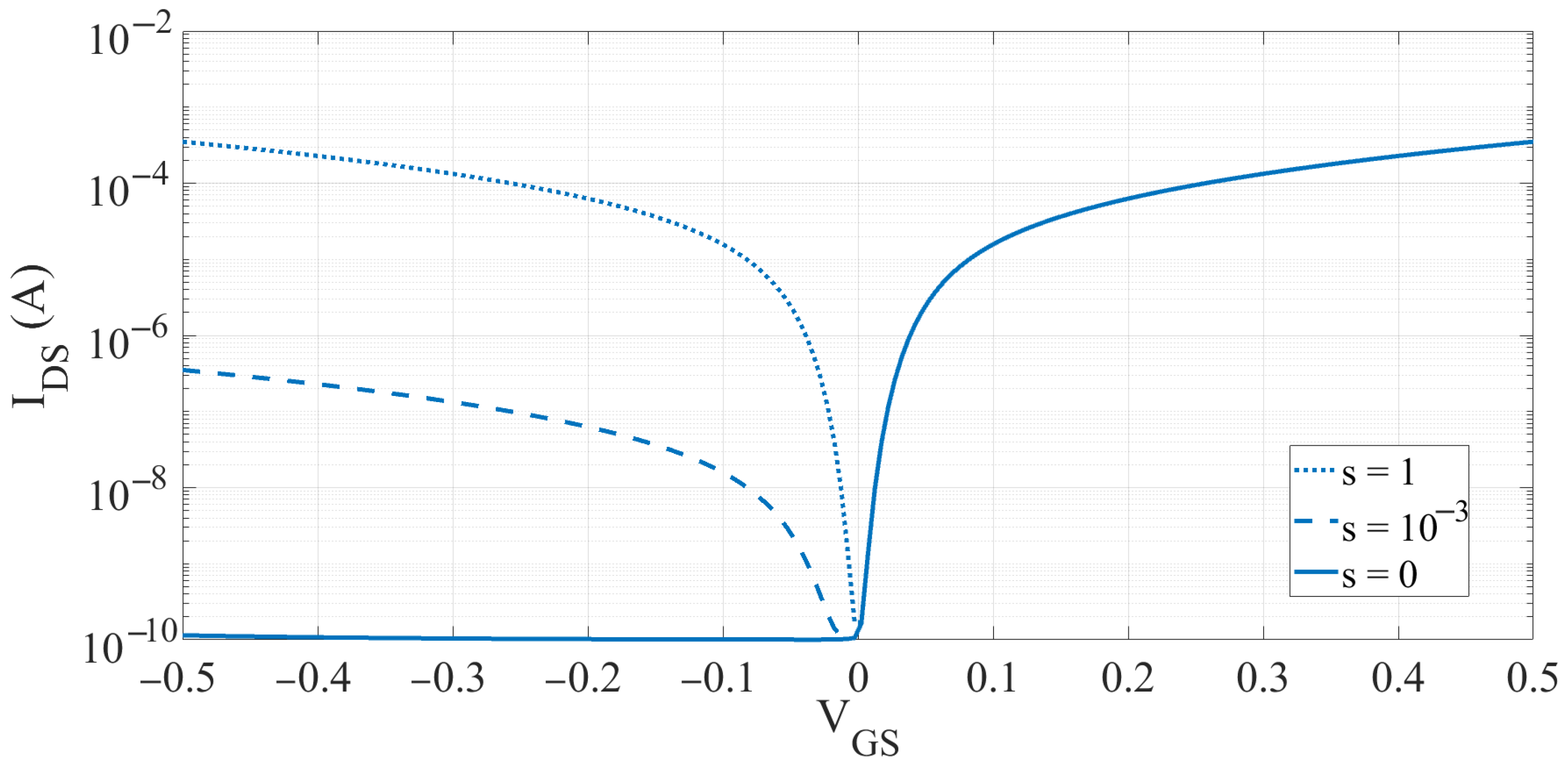
Figure 5 shows the n-TFET transcharacteristic IDS(VGS) at drain-source voltage VDS = VDD = 0.5 V for different values of the symmetric ambipolarity parameter s. Note the suppression of the ambipolarity current I A M B for the transcharacteristic having s = 0 , and a substantial I A M B comparable with the I O N for the transcharacteristic having s = 1 . Table 2 reports the main figures of Merit (FoM) for the n-type TFET device. Similar values are obtained with the p-type TFET, thanks to the full symmetry of the device. The TFET FoMs denote a superior device performance compared with commercial 3D MOSFET such as FinFETs and NS-GAAFETs [34,35,36,37]. In particular, the obtained subthreshold slope (SS) is well beyond the 60 mV/dec room temperature MOSFET limit, with also a very competitive DIBL [34,35]. As expected from the literature [4], the considered TFET also presents a poor I O N , and a considerably reduced I O F F value, around one order of magnitude less than MOSFET ones [34,35,36,37].

4.1. Functional Verification

We verify the functionality of basic logic gates (NOT, XOR, NAND, NOR) and analyze what is the effect of asymmetric ambipolarity on their logic behavior. For all the logic gates, we perform DC and transient simulations by varying V s h i f t , which corresponds to considering different amount of asymmetric ambipolar conduction due to physical and geometrical parameter variations and to process variations, as mentioned in Section 2.1. In the following, we only show the most significant cases related to the digital inverter and NAND gate, where the ambipolarity strongly impact on their fault tolerances.
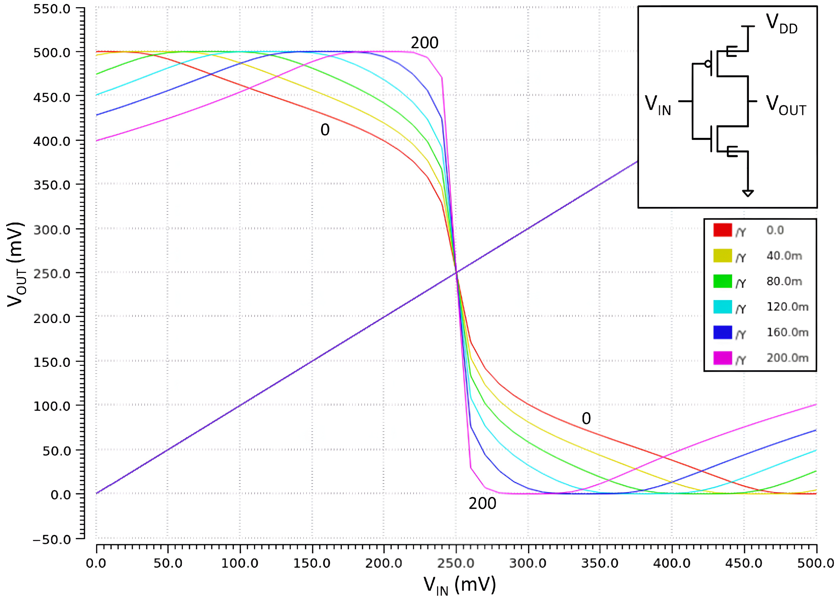
Figure 6 reports the Voltage Transfer Characteristic (VTC) V O U T ( V I N ) of the TFET-based inverter for null asymmetric ambipolarity V s h i f t = 0 (red line), and finite V s h i f t values (other colors). The V s h i f t value is varied up to 200 mV with a fixed step of 40 mV. All the VTCs present poor performances if compared with typical CMOS ones, with very low slopes, thus requiring a large transition region in which V O U T < V D D (or V O U T > 0 ) before (or after) the flex point at half of the dynamic voltage swing (0.25 V). Such a large transition region is primarily due to the poor driving strengths of the pull-up (p-type TFETs) and pull-down (n-type TFETs) networks. Indeed, because of the extremely low S S value, by sweeping the V I N from ground to V D D , a sharp increment of the sub-threshold currents of the OFF networks occurs, and the typical low TFET saturation current values do not compensate such rapid increase of leakage currents.
For finite values of V s h i f t , the asymmetric ambipolarity gradually affects the output voltage swing of the inverter, by reducing more and more its noise margins with increasing V s h i f t . For low V I N values, the gradual increase of the asymmetric ambipolarity leads to strong increment of the subthreshold current of the pull-down n-type TFET enhancing its driving strength. Because of this, the p-type TFET becomes less effective in pulling up the output line at low values of V I N . Analogous considerations hold for high values of V I N close to V D D : the strong increment of the subthreshold current of the pull-up p-type TFET enhances its driving strength and the n-type TFET becomes less effective in pulling down the output line. A more ideal behavior is instead recovered for greater/lower V I N thanks to a compensation of V s h i f t by V I N itself, causing the V O U T increase/decrease before/after the transition at half of dynamic.
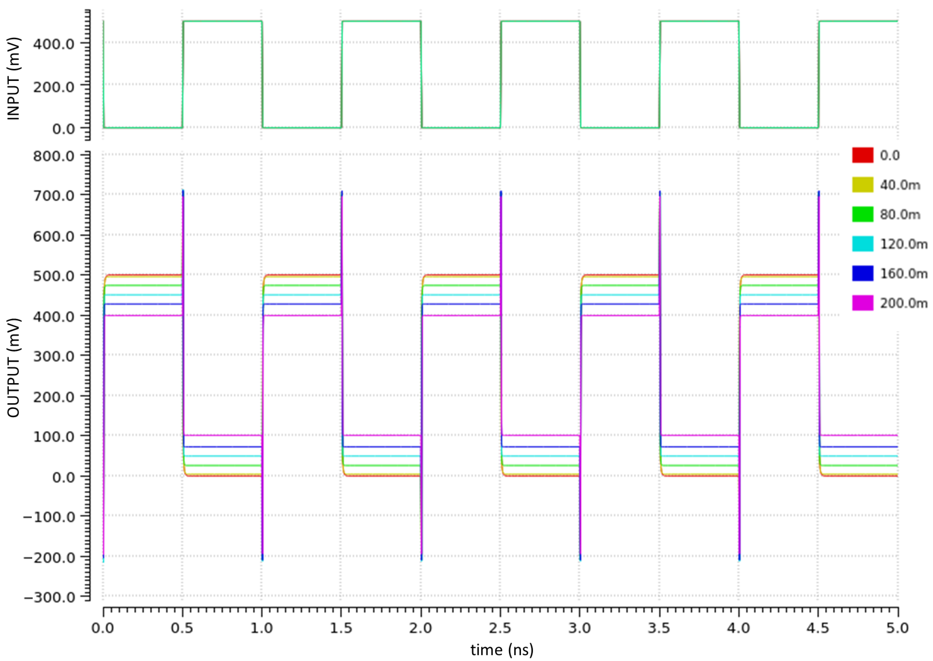
Figure 7 reports the transient simulation of the TFET-based digital inverter for different values of V s h i f t . The evident voltage peaks in the output signals are typical of TFET technology [28], and they are due to the asymmetric TFET structure, as mentioned in Section 2.1. Indeed, while in CMOS technology the symmetric conduction of MOSFETs for both positive and negative V D S permits to discharge capacitively coupled lines, for TFETs this does not happen since a reversed V D S leads to poor TFET conduction and thus long time intervals to dissipate the extra charge [28]. In the inverter case, the output voltage transients are short compared with the supposed clock period (i.e., 0.5 ns), nevertheless they are quite marked with maximum peaks that exceed V D D of 200 mV, i.e., 40% of the V D D itself (analogously for ground with −200 mV reached).
From the inspection of the output voltage dynamic evolution we notice that the effect of the asymmetric ambipolarity is to deteriorate the inverter output logic values ‘1’ ( V O H ) and ‘0’ ( V O L ). Table 3 report the V O H and V O L values sampled at steady state and the noise margins Δ V H , Δ V L of the inverter obtained as described in Section 3 by supposing the input characteristic in Figure 4 not affected by asymmetric ambipolarity ( V s h i f t = 0 ) and choosing the input logic values V I H = 450 mV and V I L = 50 mV, for which an acceptable reduction of the output logic values occurs—Figure 6. The monotonic decrement of V O H and increment of V O L , reported in Table 3 are the causes of the steep reduction of the noise margins for increasing V s h i f t . For suppressed asymetric ambipolarity the noise margins for low and high logic values results about 50 mV, whereas for V s h i f t = 80 mV they are almost halved. This 50% reduction potentially causes metastability and misinterpretation of the logic values when propagating throughout cascaded logic gates. The noise margins obtained for V s h i f t 120 mV are almost null and then negative, thus unacceptable for the propagation of the digital information, since the discrimination between the two logic values is no longer possible, and placing cascaded logic gates would cause a failure. This results is better highlighted in Figure 8, in which the percentage noise margins are reported in function of the V s h i f t values.
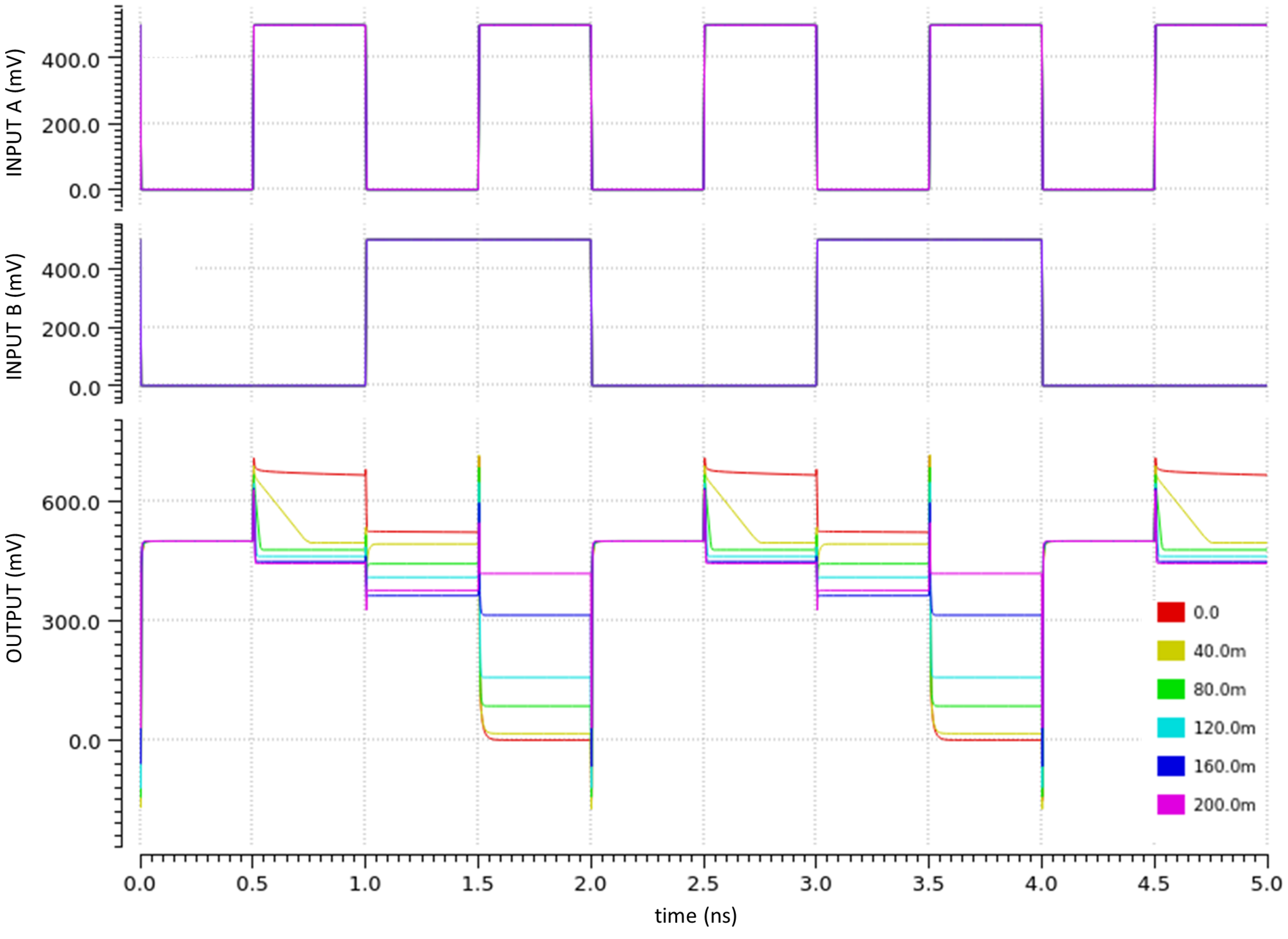
In the following, we also show the effect of asymmetric ambipolarity on NAND gate functioning, and we consider again different values of V s h i f t . The transient simulation of the NAND gate is reported in Figure 9, in which all the possible combinations of inputs are tested. As in the case of the CTFET inverter also the CTFET NAND gate presents output voltage spikes beyond the V D D and below the ground. Nevertheless, for the logic input combination A = 1 and B = 0 the output node is kept at a voltage value well beyond V D D for all the clock period, showing a slow exponential decay trend. A similar situation, but much less marked, is present also for the A = 0 and B = 1 case. The reasons are again related to the TFET impossible asymmetric conduction w.r.t. the sign of V D S , that permits extra charge discharging only through the drain to source small leakage paths [28].
Concerning instead the effect of the asymmetric ambipolarity, in the case of V s h i f t = 0 (suppressed asymmetric ambipolarity) no relevant malfunctioning of the NAND gate occurs, meaning that, analogously to the inverter case, the symmetric ambipolarity does not affect the gate functioning. This is true for all the combinations of the input. Instead, for finite V s h i f t values, there is a significant noise margin reduction, with noticeable failures for large V s h i f t values. Therefore, the asymmetric ambipolarity induces behavioral malfunctions in the NAND gate, making it unusable for logical and arithmetic operations. We report some output voltage values of interest in Table 4—low logic level ‘0’ should be ground (0 V), high logic value ‘1’ should be V D D (500 mV). A significant reduction in noise margins already occur at V s h i f t = 80 mV, with noise margins preventing cascading stages at V s h i f t = 120 mV. The NAND gate does not provide correct logic behavior for V s h i f t larger than 160 mV.

4.2. Power Analysis

We separately investigate the effect of symmetric and asymmetric ambipolarity on dissipated power in the basic CTFET logic cells. 
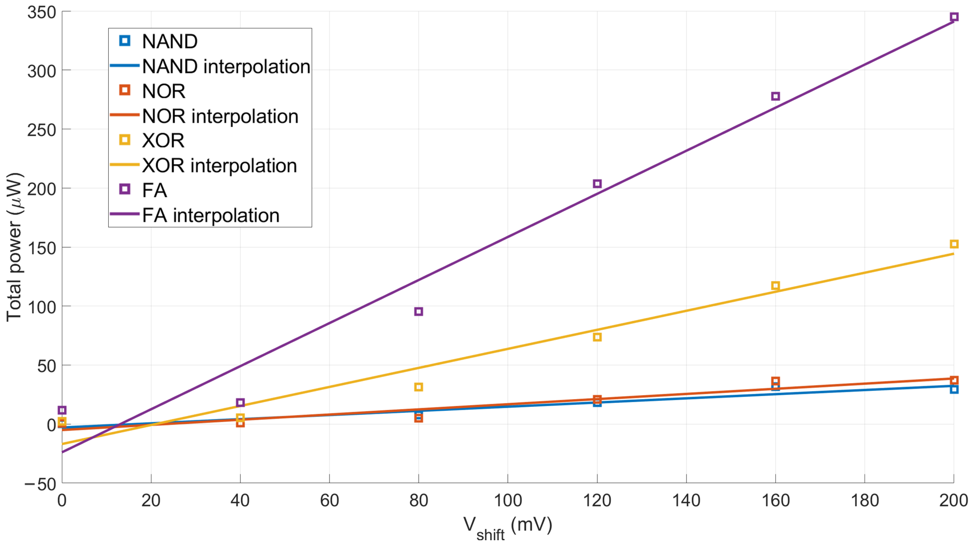
Table 5 reports the total average dissipated power, calculated with Equation (5), in function of V s h i f t for the basic two-input logic gates NAND, NOR, XOR and for the Full Adder (FA). The s parameter is fixed at s = 10 3 in all cases. As V s h i f t increases the power consumption increases more than linearly. For example, concerning the NAND gate, by passing from V s h i f t = 0 to V s h i f t = 40 mV the power consumption is doubled, while from V s h i f t = 40 mV to V s h i f t = 80 mV it increases of more than seven times and from V s h i f t = 80 mV to V s h i f t = 160 mV it increases of four times. We attribute this trend to the exponential increasing ambipolar current values that replace the OFF current values when the transcharacteristics are shifted with increasing V s h i f t -refer to Equation (1) and the discussion in Section 2.1.
Furthermore, we calculate the percentage sensitivity S V s h i f t % of the dissipated power w.r.t. V s h i f t starting from the definition of Equation (4) by exploiting the approximation reported in Equation (4). In particular, to extract the S V s h i f t % values, we interpolate the simulated data sets of Table 5 with straight lines (first order polynomial function) and we assume the angular coefficients of the best fitting straight line (in the least-squares sense) to be equal to S V s h i f t % (after normalization and multiplication by 100). The interpolations are reported in Figure 10, and the obtained sensitivity values S V s h i f t % are reported in Table 6. The minimum power consumption sensitivity to the asymmetric ambipolarity is obtained with the NAND gate, with a sensitivity of 17.66%. The sensitivity drammatically increases for more complex logical circuits (XOR and FA), achieving also the 182.52% for the FA case. The greater is the total power consumption of the considered logic gate (from NAND to FA) the larger is also the slope of the interpolating line, i.e., the sensitivity to V s h i f t , and the circuit total power consumption dependence on V s h i f t is dramatically increased if the considered digital architecture dissipates on average more power. In other words, the greater the power consumption, the greater the V s h i f t sensitivity of the dissipated power from the considered digital block.
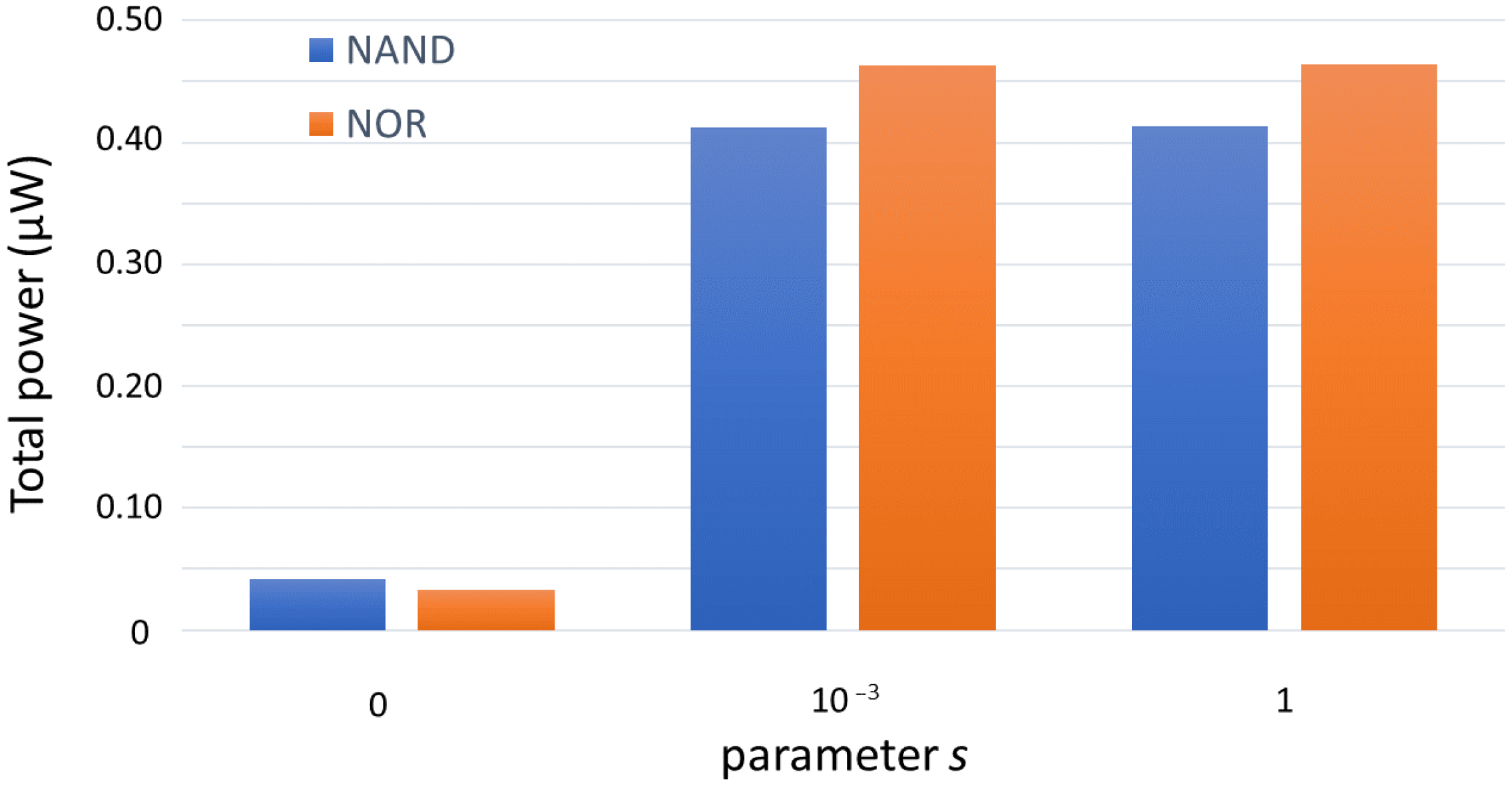
We then consider the effect of the symmetric ambipolarity on the total dissipated power. In this case, we consider only symmetric TFET transcharacteristics, i.e., we fix V s h i f t = 0 , whereas we vary the magnitude of the symmetric ambipolar conduction by changing s from 0 to 10 3 to 1. The results are reported in Table 7. For all the considered digital cells the power consumption significantly increases when s is increased. In particular, it dramatically increases of around one order of magnitude when s is increased from 0 (no ambipolarity) to 10 3 (suppressed ambipolarity) for the NAND and the NOR gates. Then by further increasing s from 10 3 (suppressed ambipolarity) to 1 (full ambipolar device) only a slight increase occurs. This trend is well highlighted in Figure 11, where the increase in dissipated power from the case of s = 10 3 to the case of s = 1 is not appreciable.
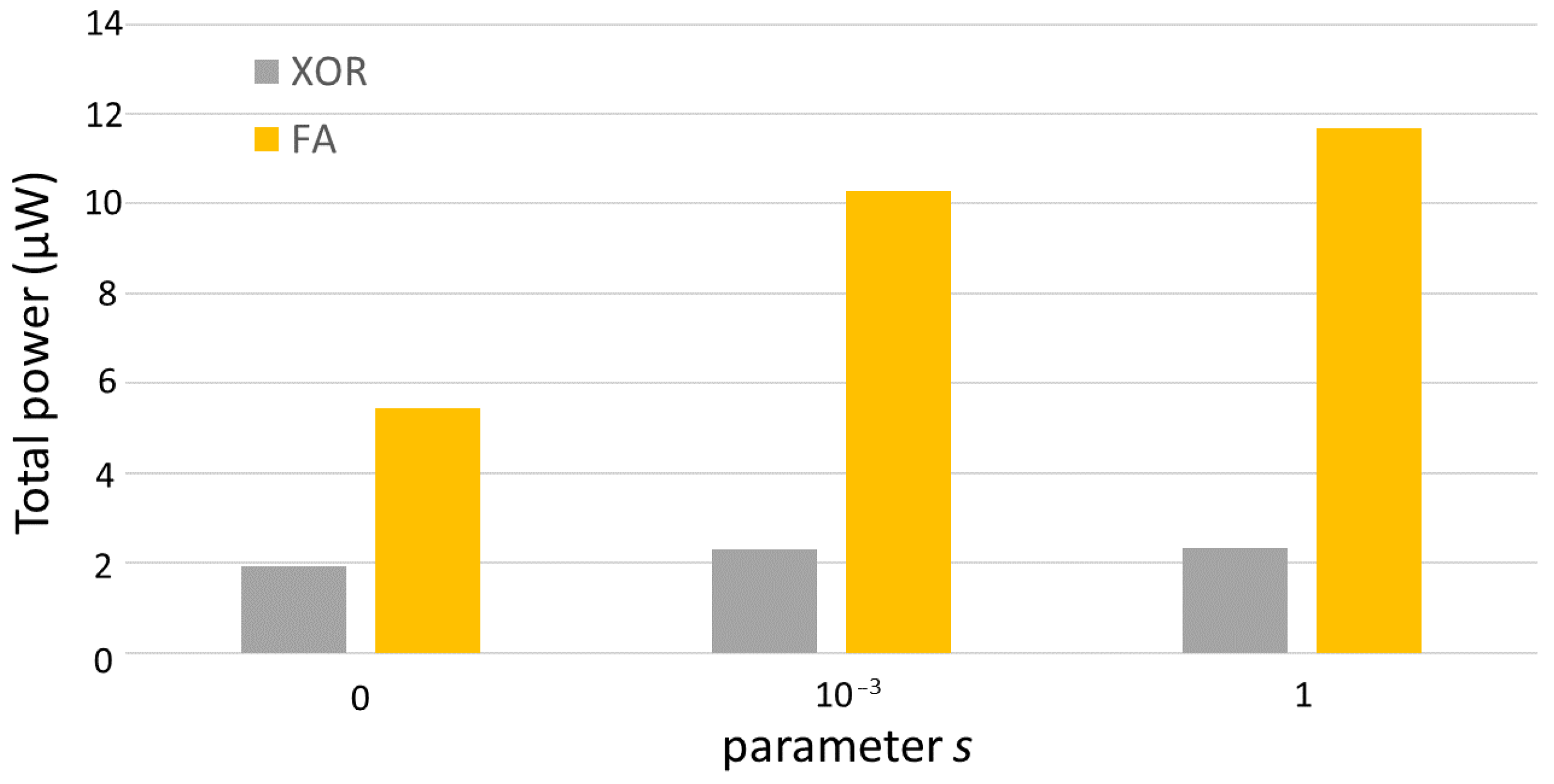
Similar considerations hold for more complex digital cells, namely the XOR and the FA. Nevertheless, we notice that for more complex cells, the increase in power consumption, due to s increase from 0 to 10 3 , is much less marked than for the simpler NAND and NOR cells, as reported in Figure 12. Thus, we separately calculate the dissipated power sensitivity through Equation (4) for all the considered gates for the s increase from 0 to 10 3 and for the s increase from 10 3 and then to 1. We call the first S s : 0 10 3 % and the latter S s : 10 3 1 % and we report the result in Table 8. The sensitivity to ambipolar current magnitude is extremely larger for s passing from 0 to 10 3 than for s passing from 10 3 to 1. Even if more complex digital blocks present reduced sensitivity to s, the trend is confirmed. Because of the direct proportionality of I A M B to s (see Equation (2)) our results reflect in the following: an I A M B three orders of magnitude lower than I O N values is still leading to important non-ideality power consumption and the dissipated power is very sensitive to I A M B , thus also small reductions of I A M B will result in large power consumption reduction.

5. Conclusions

We investigated through Cadence Virtuoso SPICE simulations the effect of the symmetric and asymmetric ambipolar transcharacteristics in TFET-based complementary logic circuits. We modeled the asymmetric ambipolarity through a DC voltage generator V s h i f t on the TFET gates, to emulate the transcharacteristics shift, whereas we exploited the s parameter employed in Hao Lu Verilog-A model to account for the effect of the symmetric ambipolarity.
Our results show that symmetric ambipolarity has small effect on complementary logic circuit functioning, while asymmetric ambipolarity, if not kept under control, can lead to strong reduction of noise margins and evident behavioral failure.
Alongside behavioral analysis of circuits we also analyzed the effects of ambipolarity on dissipated power in digital circuits. In this case both the symmetric and asymmetric ambipolarity lead to relevant power performance deterioration. Asymmetric ambipolarity doubles the dissipated power for almost all the considered basic logic circuits, already for few tens of mV of transcharacteristic shift. We verified that the digital circuit dissipated power sensitivity to asymmetric ambipolarity increases with system complexity. In the case of symmetric ambipolarity, the dissipated power sensitivity to I A M B is extremely high for small variations of I A M B when it is order of magnitudes lower than the I O N , whereas the system is less sensible to I A M B variations when I A M B approaches I O N values. Therefore, even small reductions in I A M B can significantly reduce the dissipated power in complementary TFET digital circuits.
We believe our work to clarify the effects of ambipolar conduction on logic failure and power performance of complementary digital circuits based on TFET technology. Moreover, we believe it to motivate future technological efforts to further suppress the ambipolar current in TFETs and to keep under control the TFET transcharacteristic shift due to inaccurate gate engineering and fabrication process variations.

Author Contributions

Conceptualization, G.P., M.V., C.E.S., F.M. and Y.A.; methodology, R.A.C., F.M. and C.E.S.; software/simulations, R.A.C.; formal analysis, C.E.S. and F.M.; investigation, R.A.C., C.E.S. and F.M.; resources, M.R.R. and M.V.; data curation, R.A.C.; writing—original draft preparation, F.M. and C.E.S.; writing—review and editing, Y.A., G.P. and M.V.; visualization, C.E.S. and F.M.; supervision, G.P., M.V., F.M., C.E.S. and Y.A.; project administration, Y.A., G.P., M.V. and M.R.R.; internal funding acquisition, G.P. and M.R.R. All authors have read and agreed to the published version of the manuscript.

Funding

This research received no external funding.

Institutional Review Board Statement

Not applicable.

Informed Consent Statement

Not applicable.

Data Availability Statement

All the needed data are reported in the article.

Conflicts of Interest

The authors declare no conflict of interest.

References

  1. Taur, Y.; Ning, T.H. Fundamentals of Modern VLSI Devices, 2nd ed.; Cambridge University Press: Cambridge, UK, 2009. [Google Scholar] [CrossRef]
  2. Roy, K.; Prasad, S. Low-Power Cmos Vlsi Circuit Design; Wiley India Pvt. Ltd.: New Delhi, India, 2009. [Google Scholar]
  3. Shafique, M.; Garg, S.; Henkel, J.; Marculescu, D. The EDA Challenges in the Dark Silicon Era: Temperature, Reliability, and Variability Perspectives. In Proceedings of the 51st Annual Design Automation Conference, San Francisco, CA, USA, 1–5 June 2014; Association for Computing Machinery: New York, NY, USA, 2014; pp. 1–6. [Google Scholar] [CrossRef]
  4. Ionescu, A.M.; Riel, H. Tunnel field-effect transistors as energy-efficient electronic switches. Nature 2011, 479, 329–337. [Google Scholar] [CrossRef] [PubMed]
  5. Seabaugh, A.C.; Zhang, Q. Low-Voltage Tunnel Transistors for Beyond CMOS Logic. Proc. IEEE 2010, 98, 2095–2110. [Google Scholar] [CrossRef]
  6. International Roadmap for Devices and Systems—Executive Report; IEEE: Piscataway, NJ, USA, 2021.
  7. Aswathy, M.; Biju, N.M.; Komaragiri, R. Comparison of a 30nm Tunnel Field Effect Transistor and CMOS Inverter Characteristics. In Proceedings of the 2013 Third International Conference on Advances in Computing and Communications, Cochin, India, 29–31 August 2013; pp. 149–152. [Google Scholar]
  8. Núñez, J.; Avedillo, M.J. Comparison of TFETs and CMOS Using Optimal Design Points for Power–Speed Tradeoffs. IEEE Trans. Nanotechnol. 2017, 16, 83–89. [Google Scholar] [CrossRef] [Green Version]
  9. Rendón, M.; Cao, C.; Landázuri, K.; Garzón, E.; Prócel, L.M.; Taco, R. Performance Benchmarking of TFET and FinFET Digital Circuits from a Synthesis-Based Perspective. Electronics 2022, 11, 632. [Google Scholar] [CrossRef]
  10. Strangio, S.; Settino, F.; Palestri, P.; Lanuzza, M.; Crupi, F.; Esseni, D.; Selmi, L. Digital and analog TFET circuits: Design and benchmark. Solid-State Electron. 2018, 146, 50–65. [Google Scholar] [CrossRef] [Green Version]
  11. Strangio, S.; Palestri, P.; Lanuzza, M.; Crupi, F.; Esseni, D.; Selmi, L. Assessment of InAs/AlGaSb Tunnel-FET Virtual Technology Platform for Low-Power Digital Circuits. IEEE Trans. Electron Devices 2016, 63, 2749–2756. [Google Scholar] [CrossRef]
  12. Lu, H.; Paletti, P.; Li, W.; Fay, P.; Ytterdal, T.; Seabaugh, A. Tunnel FET Analog Benchmarking and Circuit Design. IEEE J. Explor.—Solid-State Comput. Devices Circuits 2018, 4, 19–25. [Google Scholar] [CrossRef]
  13. Knoll, L.; Zhao, Q.T.; Nichau, A.; Trellenkamp, S.; Richter, S.; Schäfer, A.; Esseni, D.; Selmi, L.; Bourdelle, K.; Mantl, S. Inverters With Strained Si Nanowire Complementary Tunnel Field-Effect Transistors. IEEE Electron Device Lett. 2013, 34, 813–815. [Google Scholar] [CrossRef]
  14. Tomioka, K.; Yoshimura, M.; Fukui, T. Steep-slope tunnel field-effect transistors using III–V nanowire/Si heterojunction. In Proceedings of the 2012 Symposium on VLSI Technology (VLSIT), Honolulu, HI, USA, 12–14 June 2012; pp. 47–48. [Google Scholar] [CrossRef]
  15. Bhuwalka, K.; Schulze, J.; Eisele, I. Scaling the vertical tunnel FET with tunnel bandgap modulation and gate workfunction engineering. IEEE Trans. Electron Devices 2005, 52, 909–917. [Google Scholar] [CrossRef]
  16. Boucart, K. Double-Gate Tunnel FET with High-κ Gate Dielectric; IEEE: Piscataway, NJ, USA, 2008. [Google Scholar]
  17. Toh, E.H.; Wang, G.H.; Samudra, G.; Yeo, Y.C. Device physics and design of double-gate tunneling field-effect transistor by silicon film thickness optimization. Appl. Phys. Lett. 2007, 90, 263507. [Google Scholar] [CrossRef]
  18. Lu, H.; Seabaugh, A. Tunnel Field-Effect Transistors: State-of-the-Art. IEEE J. Electron Devices Soc. 2014, 2, 44–49. [Google Scholar] [CrossRef]
  19. Lin, Z.; Chen, P.; Ye, L.; Yan, X.; Dong, L.; Zhang, S.; Yang, Z.; Peng, C.; Wu, X.; Chen, J. Challenges and Solutions of the TFET Circuit Design. IEEE Trans. Circuits Syst. Regul. Pap. 2020, 67, 4918–4931. [Google Scholar] [CrossRef]
  20. Mamidala, J.; Vishnoi, R.; Pandey, P. Tunnel Field-Effect Transistors (TFET): Modelling and Simulation; Wiley: Hoboken, NJ, USA, 2016. [Google Scholar]
  21. Saurabh, S.; Kumar, M. Fundamentals of Tunnel Field-Effect Transistors; CRC Press: Boca Raton, FL, USA; Taylor & Francis Group: Abingdon, UK, 2016. [Google Scholar]
  22. Pasupathy, K.R.; Manivannan, T.S.; Lakshminarayanan, G. A Review of Engineering Techniques to Suppress Ambipolarity in Tunnel FET. Silicon 2022, 14, 1887–1894. [Google Scholar] [CrossRef]
  23. Hraziia; Vladimirescu, A.; Amara, A.; Anghel, C. An analysis on the ambipolar current in Si double-gate tunnel FETs. Solid State Electron. 2012, 70, 67–72. [Google Scholar] [CrossRef]
  24. Nigam, K.; Kondekar, P.; Sharma, D. Approach for ambipolar behaviour suppression in tunnel FET by workfunction engineering. Micro Nano Lett. 2016, 11, 460–464. [Google Scholar] [CrossRef]
  25. Zhou, G.; Lu, Y.; Li, R.; Zhang, Q.; Hwang, W.; Liu, Q.; Vasen, T.; Chen, C.; Zhu, H.; Kuo, J.M.; et al. Vertical InGaAs/InP tunnel FETs with tunneling normal to the gate. EEE Electron Device Lett. 2011, 32, 1516–1518. [Google Scholar] [CrossRef]
  26. Lu, H.; Esseni, D.; Seabaugh, A. Universal analytic model for tunnel FET circuit simulation. Solid-State Electron. 2015, 108, 110–117. [Google Scholar] [CrossRef]
  27. Avci, U.E.; Morris, D.H.; Hasan, S.; Kotlyar, R.; Kim, R.; Rios, R.; Nikonov, D.E.; Young, I.A. Energy efficiency comparison of nanowire heterojunction TFET and Si MOSFET at Lg = 13nm, including P-TFET and variation considerations. In Proceedings of the 2013 IEEE International Electron Devices Meeting, Washington, DC, USA, 9–11 December 2013; pp. 33.4.1–33.4.4. [Google Scholar] [CrossRef]
  28. Morris, D.H.; Avci, U.E.; Rios, R.; Young, I.A. Design of Low Voltage Tunneling-FET Logic Circuits Considering Asymmetric Conduction Characteristics. IEEE J. Emerg. Sel. Top. Circuits Syst. 2014, 4, 380–388. [Google Scholar] [CrossRef]
  29. Lee, C.S.; Pop, E.; Franklin, A.D.; Haensch, W.; Wong, H.S.P. A Compact Virtual-Source Model for Carbon Nanotube FETs in the Sub-10-nm Regime—Part I: Intrinsic Elements. IEEE Trans. Electron Devices 2015, 62, 3061–3069. [Google Scholar] [CrossRef] [Green Version]
  30. Liu, H.; Saripalli, V.; Narayanan, V.; Datta, S. III-V Tunnel FET Model; nanoHUB: West Lafayette IN, USA, 2015. [Google Scholar] [CrossRef]
  31. Mo, F.; Spano, C.E.; Ardesi, Y.; Piccinini, G.; Graziano, M. Beyond-CMOS Artificial Neuron: A Simulation- Based Exploration of the Molecular-FET. IEEE Trans. Nanotechnol. 2021, 20, 903–911. [Google Scholar] [CrossRef]
  32. Hussain, I.; Riente, F.; Roch, M.R.; Piccinini, G.; Graziano, M. Performance analysis of transistor-based circuits through TAMAMS Web: From bulk to molecular devices. In Proceedings of the 2016 5th International Conference on Electronic Devices, Systems and Applications (ICEDSA), Ras Al Khaimah, United Arab Emirates, 6–8 December 2016; pp. 1–4. [Google Scholar] [CrossRef]
  33. Lu, Y.; Zhou, G.; Li, R.; Liu, Q.; Zhang, Q.; Vasen, T.; Chae, S.D.; Kosel, T.; Wistey, M.; Xing, H.; et al. Performance of AlGaSb/InAs TFETs with gate electric field and tunneling direction aligned. IEEE Electron Device Lett. 2012, 33, 655–657. [Google Scholar] [CrossRef]
  34. Choi, Y.K.; Lindert, N.; Xuan, P.; Tang, S.; Ha, D.; Anderson, E.; King, T.J.; Bokor, J.; Hu, C. Sub-20 nm CMOS FinFET technologies. In Proceedings of the International Electron Devices Meeting, Technical Digest (Cat. No.01CH37224), Washington, DC, USA, 2–5 December 2001; pp. 19.1.1–19.1.4. [Google Scholar] [CrossRef]
  35. Agrawal, A.; Chouksey, S.; Rachmady, W.; Vishwanath, S.; Ghose, S.; Mehta, M.; Torres, J.; Oni, A.; Weng, X.; Li, H.; et al. Gate-All-Around Strained Si0.4Ge0.6 Nanosheet PMOS on Strain Relaxed Buffer for High Performance Low Power Logic Application. In Proceedings of the 2020 IEEE International Electron Devices Meeting (IEDM), San Francisco, CA, USA, 12–18 December 2020; pp. 2.2.1–2.2.4. [Google Scholar] [CrossRef]
  36. Zhang, J.; Frougier, J.; Greene, A.; Miao, X.; Yu, L.; Vega, R.; Montanini, P.; Durfee, C.; Gaul, A.; Pancharatnam, S.; et al. Full Bottom Dielectric Isolation to Enable Stacked Nanosheet Transistor for Low Power and High Performance Applications. In Proceedings of the 2019 IEEE International Electron Devices Meeting (IEDM), San Francisco, CA, USA, 7–11 December 2019; pp. 11.6.1–11.6.4. [Google Scholar] [CrossRef]
  37. Loubet, N.; Hook, T.; Montanini, P.; Yeung, C.W.; Kanakasabapathy, S.; Guillom, M.; Yamashita, T.; Zhang, J.; Miao, X.; Wang, J.; et al. Stacked nanosheet gate-all-around transistor to enable scaling beyond FinFET. In Proceedings of the 2017 Symposium on VLSI Technology, Kyoto, Japan, 5–8 June 2017; pp. T230–T231. [Google Scholar] [CrossRef]
Figure 1. TFET device conceptual structure and operating principle. (a) Basic n-type TFET device structure; (b) equilibrium band diagram for the device in (a); (c) ON state band diagram for the device in (a); (d) OFF state band diagram for the device in (a); (e) ambipolar state band diagram for the device in (a).
Jlpea 12 00058 g001
Figure 2. Examples of ambipolar n-type TFET transcharacteristics. (a) Example of TFET suffering of symmetric ambipolarity: symmetric transcharacteristics with different ambipolar currents; (b) Example of TFET suffering of asymmetric ambipolarity: asymmetric transcharacteristics with different shift w.r.t. ideal (red) one.
Jlpea 12 00058 g002
Figure 3. Structure of vertical AlGaSb/InAs heterojunction TFET. L G is the gate length, L S the spacer length, L D the spacer-drain overlapping length, and L U C the undercut length.
Jlpea 12 00058 g003
Figure 4. Logical parameters and noise margins definition.
Jlpea 12 00058 g004
Figure 5. The device transcharacteristic IDS(VGS) at V D S = VDD for different values of the s parameter.
Jlpea 12 00058 g005
Figure 6. TFET-based inverter transcharacteristics at different V s h i f t values: red (null shift), yellow 40 mV, green 80 mV, light blue 120 mV, dark blue 160 mV, purple 200 mV. The blue straight line corresponds to the V O U T = V I N straight line. The top-right inset shows the CTFET inverter schematic.
Jlpea 12 00058 g006
Figure 7. Transient simulation of the TFET-based digital inverter for different values of V s h i f t : red (null shift), yellow 40 mV, green 80 mV, light blue 120 mV, dark blue 160 mV, purple 200 mV. The green signal is the input signal.
Jlpea 12 00058 g007
Figure 8. Noise margins percentage of TFET-based inverter as function of different values of V s h i f t . The orange bar represents the percentage noise margin for low logic value, whereas the blue one the reduction of noise margin for high logic value.
Jlpea 12 00058 g008
Figure 9. NAND gate time transient simulation with different TFET transcharacteristic shift values: red (no shift), yellow 40 mV, green 80 mV, light blue 120 mV, dark blue 160 mV, purple 200 mV.
Jlpea 12 00058 g009
Figure 10. Total dissipated power for the basic logic gates as a function of V s h i f t . The markers are the simulated data, the straight lines are the first order polynomial interpolations (least-squares sense). The negative power values obtained for small V s h i f t values-below 20 mV-are artifacts due to the interpolation through a linear polynomial function.
Jlpea 12 00058 g010
Figure 11. Total power dissipation in function of the amount of symmetric ambipolarity (s value) for the NAND and the NOR gates.
Jlpea 12 00058 g011
Figure 12. Total power dissipation in function of the amount of symmetric ambipolarity (s value) for the XOR and the FA digital circuits.
Jlpea 12 00058 g012
Table 1. Physical and geometrical parameters of the considered AlGaSb/InAs heterojunction TFET.
Parameter DescriptionValue
Metal gate workfunction4.93 eV
Al2O3 thickness1.4 nm
AlGaSb source doping4 × 10 18 cm 3
Source δ doping plane doping6 × 10 12 cm 3
InAs channel doping5 × 10 17 cm 3
Gate length L G 20 nm
Undercut length L U C 10 nm
Spacer length L S 10 nm
Spacer-drain overlapping length L D 10 nm
Table 2. Calculated FoM for vertical AlGaSb/InAs heterojunction TFET.
SS (mV/dec)DIBL (mV/V)ION (μA)IOFF ( pA)ION/IOFF
1311351.19111.223.16 × 106
Table 3. Output logic values and noise margin of the TFET-based inverter as a function of the asymmetric ambipolarity parameter V s h i f t .
Inverter Output Values and Noise Margins (mV)
Vshift = 0 mV40 mV80 mV120 mV160 mV200 mV
V O H 499.992495.742474.057450.711427.853389.934
V O L 0.0084.25825.94249.28972.146101.066
Δ V H 49.99245.74224.0570.711−22.147−60.066
Δ V L 49.99245.74224.0580.711−22.14651.066
Table 4. Output voltage in mV for the two-input NAND gate for the considered V s h i f t values. A and B are the two inputs of the NAND gate, logic 0 is encoded through a 0 V voltage value while logic 1 is encoded through an 500 mV voltage value. The chosen input combinations highlight the NAND malfunctioning when V s h i f t is increased.
NAND Output Voltage (mV)
Vshift = 0 mV40 mV80 mV120 mV160 mV200 mV
A = 0 B = 1523.07492.85443.06409.11362.88376.23
A = 1 B = 124.28 × 10 3 16.2285.34157.51313.86418.44
Table 5. Total power dissipation depending on the asymmetric ambipolarity for parameter Vshift.
Total Power (μW)
Vshift = 0 mV40 mV80 mV120 mV160 mV200 mV
NAND413 × 10−31.047.7618.2431.6129.41
NOR464 × 10−3957 × 10−34.9120.9236.5337.02
XOR2.325.4231.2973.56117.40152.46
FA11.6718.0395.18203.70277.90345.10
Table 6. Total dissipated power percentage sensitivity to Vshift, indicated with S V s h i f t % .
NANDNORXORFA
S V s h i f t % 17.66%21.82%80.64%182.52%
Table 7. Total power dissipation depending on the asymmetric ambipolarity for parameter s.
Total Power ( μ W)
s = 0s = 0.001s = 1
NAND41.60 × 10−3412.30 × 10−3413.00 × 10−3
NOR32.73 × 10−3463 × 10−3464 × 10−3
XOR1.922.302.32
FA5.4610.2711.67
Table 8. Total dissipated power percentage sensitivity to s parameter.
NANDNORXORFA
S 0 10 3 % 1.633 × 10 5 %1.736 × 10 5 %1.8 × 10 4 %611 × 10 4 %
S 10 3 1 % 0.17%0.22%0.87%12.77%
Publisher’s Note: MDPI stays neutral with regard to jurisdictional claims in published maps and institutional affiliations.

