Article

A gm/ID-Based Design Strategy for IoT and Ultra-Low-Power OTAs with Fast-Settling and Large Capacitive Loads

by
Gianluca Giustolisi
* and
Gaetano Palumbo
Dipartimento di Ingegneria Elettrica Elettronica e Informatica (DIEEI), Università degli Studi di Catania, Viale A. Doria 6, I-95125 Catania, Italy
*
Author to whom correspondence should be addressed.
J. Low Power Electron. Appl. 2021, 11(2), 21; https://doi.org/10.3390/jlpea11020021
Submission received: 31 March 2021 / Revised: 7 May 2021 / Accepted: 8 May 2021 / Published: 12 May 2021

Abstract

:
In this paper, a new strategy for the design of ultra-low-power CMOS operational transconductance amplifiers (OTAs), using the g m / I D approach, is proposed for the Internet-of-things (IoT) scenario. The strategy optimizes the speed/dissipation of the OTA in terms of settling time, including slew-rate effects. It was designed for large capacitive loads and for transistors biased in the sub-threshold region, but it is also suitable for low-capacitive loads or for transistors biased in the saturation region. To validate the proposed strategy, a well-known three-stage OTA was designed starting from capacitive load and settling time requirements. Simulations confirmed that the OTA satisfies the specifications (even under Monte Carlo analysis), thus proving the correctness of the proposed approach.

1. Introduction

At present, the Internet of things (IoT) paradigm is certainly playing a crucial role in the electronic market. It is estimated that more than 30 billion devices are operating in a wide range of applications that span from health-care to agriculture or from industrial manufacturing to automotive, if only to mention the most significant [1]. As is well known, an IoT node is required to have sensing, processing and wireless capabilities [2,3]. Sensing means that the IoT node is interfaced with different kinds of sensors whose analog signals (e.g., temperature, pressure, humidity, CO 2 , light, acceleration, etc.) must be read correctly by a proper sensing circuitry. Processing means that the IoT node converts the sensor signals into digital words that are subsequently elaborated, as requested by the given application. Wireless means that the IoT node can send/receive data to/from other nodes or a central processing unit. In addition to these features, it is not uncommon to deal with applications that require energetically autonomous IoT nodes, a section of which is dedicated to the energy harvesting from the environment [4,5,6] and to the management of such harvested power [7,8,9,10]. Whatever the overall application or the specific sub-circuit of the IoT node, energy efficiency is one of paramount factors to survive in the semiconductor market and therefore, wise energy management is a critical task to be addressed during the design phase.
As far as the analog section is concerned, the optimization of the power consumption is mainly accomplished by reducing the operating voltage (1 V or less). This makes the analog section compatible with the same sub-100 nm CMOS process adopted for the digital circuitry, which, in general, occupies the larger amount of silicon area. In the ultra-low-power context, the bias current must also be reduced but at the expense of an increased noise level and of a slower operating speed. In this scenario, the design is not a straightforward task because the technology scaling, the low supply voltage and the low bias current introduce many degenerative effects.
In particular, the reduction in the MOSFET intrinsic gain ( g m r d 10 ), in the dynamic-range and in the signal-to-noise ratio can severely affect the circuit performance [11,12,13,14,15,16,17,18].
Among the different analog circuits that coexist in an IoT node, the operational transconductance amplifier (OTA) is a very common and versatile analog building block [19,20,21,22,23]. For its characteristics, it suits the sensing section, where high precision and moderate bandwidth are required. Due to the reduction in the power supply voltage, multistage topologies are often adopted in these amplifiers, and the optimization of the power consumption must face with noise, dynamic range and speed trade-offs [24,25,26,27,28,29,30,31,32,33,34,35,36]. Ultra-low-power amplifiers cut down the power consumption by biasing all the transistors in the sub-threshold region; however, the speed requirements are more arduous to fulfill also because the slew-rate effects produce serious limitations.
In this paper, we propose a new strategy for the design of ultra-low-power CMOS OTAs using the g m / I D approach. Because of its wide knowledge and diffusion, we focus our attention on the three-stage OTA based on the reverse nested Miller compensation with a feed-forward stage (RNMC-FF) and to the case of large capacitive loads. Differently from the past works reported in the literature [37,38,39,40,41,42,43,44,45,46,47,48,49], the proposed design strategy (a) optimizes the speed/dissipation of the amplifier taking into account the settling time and the slew-rate effects; (b) despite being developed for large capacitive loads, it also holds for low-capacitive loads; and (c) despite being developed for the transistors biased in the sub-threshold region, it also holds for the saturation one.
The paper is structured as follows. In Section 2, the OTA topology is presented at the block schematic level and at the transistor-level implementation. Section 3 discusses the design strategy focusing the attention on the g m / I D approach, to the sub-threshold region, to the settling time (in terms of small- and large-signal behavior), to the noise specification, and to the optimization of the overall power dissipation. In Section 4, an RNMC-FF three-stage OTA was designed and validated through simulations. Finally, in Section 5, conclusions are drawn.

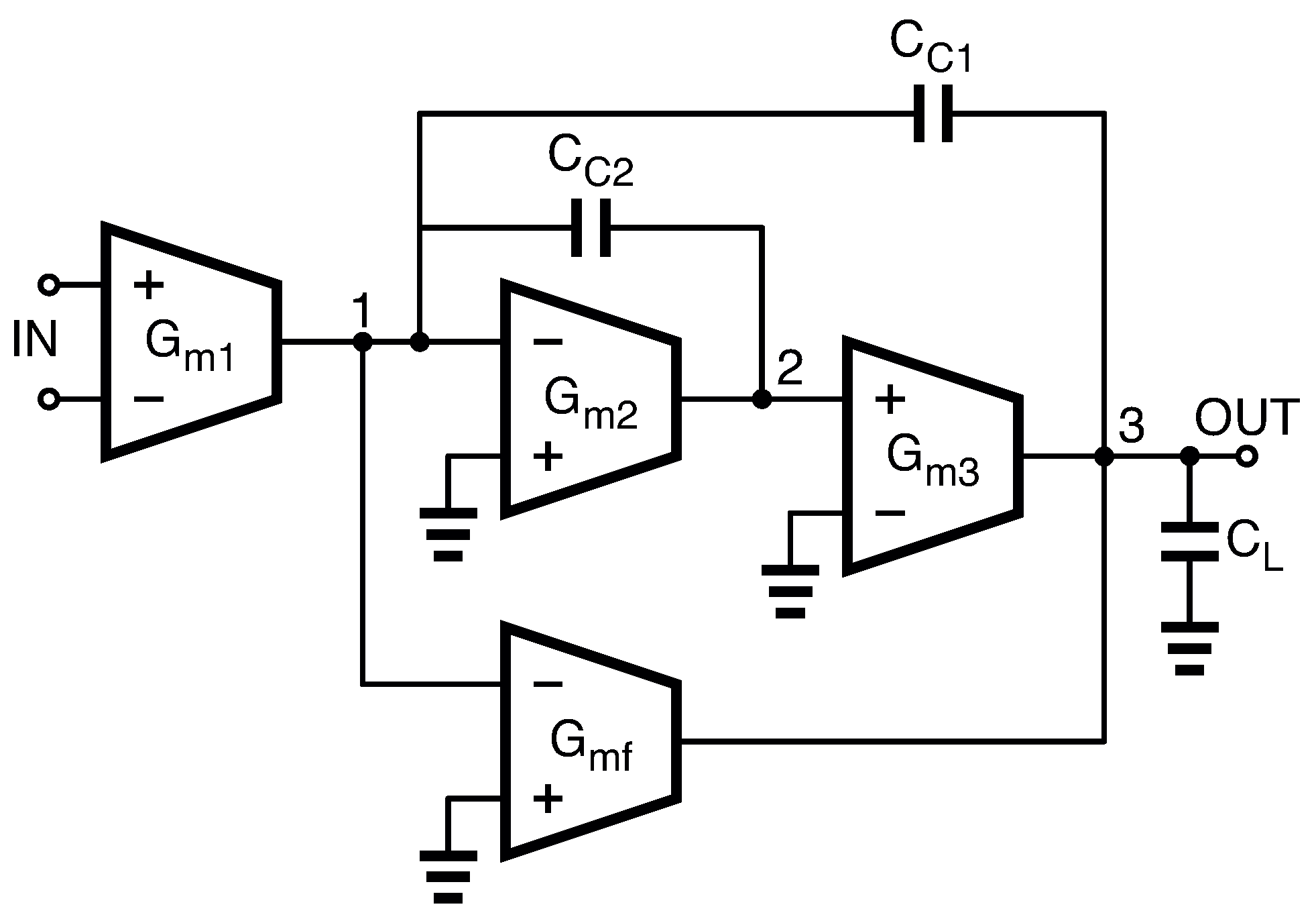
2. The Three-Stage OTA

The design strategy, which will be introduced in the next section, was applied to the three-stage OTA whose simplified block schematic is shown in Figure 1.
The OTA is made up of three main transconductors, G m i , whose output terminals are connected to the respective i-th node of the overall amplifier. In general, the first transconductor, G m 1 , is a differential-input stage that better rejects external disturbances. The second and the third transconductors, G m 2 and G m 3 , are implemented using an inverting stage and a non-inverting one. The stability is achieved using the reverse nested Miller compensation (RNMC) made up of a main compensation capacitor, C C 1 , connected between nodes 3 and 1, and a secondary compensation capacitor, C C 2 , connected between nodes 2 and 1. It is worth noting that, under equal design specifications, RNMC topologies are intrinsically faster than nested Miller compensated counterparts, since the inner capacitor of the RNMC network is not connected to the output node [50,51].
Some RNMC topologies also adopt a nulling resistor to improve the compensation in terms of bandwidth/consumption performance [51]. However, its resistance must be made proportional to the reciprocal of the amplifier transconductances that, in an ultra-low-power design, can be in the order of few microsiemens or less. Therefore, the resulting resistance would be in the order of hundreds of kiloohms and this, in turn, would worsen both area and noise performance. For this reason, in our design, we preferred not to use any nulling resistor and maintained the simplest possible compensation network.
An additional transconductor, G mf , makes a feed-forward (FF) path that allows some simplifications in the transfer function and helps the final stage drive large capacitive loads. In general, this additional stage is obtained without any further current dissipation but by simply connecting the bias transistor of the third stage to the output node of the first transconductor. Equivalent output resistances, R o 1 , R o 2 and R o 3 (not shown in the figure), are assumed as placed between the output node of each i-th transconductor and the ground, respectively. Similarly, parasitic capacitors, C o 1 and C o 2 , are assumed to be in parallel to R o 1 and R o 2 . However, in our models, we can neglect these output resistances and parasitic capacitors, provided that G m i R o i 1 and C C 1 , C C 2 C o 1 , C o 2 , respectively.
A transistor-level implementation of the block schematic depicted in Figure 1 is shown in Figure 2. In particular, the circuit is designed using a 65 nm CMOS process and is optimized for operating at the V DD = 1 V taking advantage of the three types of complementary transistors that differ for the threshold voltage.
Low-threshold (LVT) transistors are used for the two input devices of the differential pair. In this manner, we optimize the common-mode input range that is bounded by
V GS 3 , 6 V SG 1 , 2 + V SD 1 , 2 sat V cm , in V DD V SD 5 sat V SG 1 , 2 .
High-threshold (HVT) transistors are used for the current mirror M9-M10. This makes the gate–source voltage of M9 similar to the source–drain bias voltage of M10 and reduces the systematic error of the current mirror due to channel-length modulation. High-threshold transistors are also used in M12 and M14 of the slew-rate (SR) enhancer but their role shall be discussed in the following. Regular-threshold (RVT) transistors are used for the remaining active devices of the OTA.
With respect to the transistor transconductances, the stage transconductances of the block schematic in Figure 1 are G m 1 = g m 1 , 2 , G m 2 = g m 6 , G m 3 = g m 8 ( g m 10 / g m 9 ) = r g m 8 and G mf = g m 11 . Bias currents 2 I 1 and I 2 are provided through current mirrors M5-MBP and M7-MBP, respectively. As we mentioned before, the feed-forward transconductor, G mf , is implemented by simply connecting the gate of M11 to node v 1 . This also sets the bias current of the third stage to I 3 = ( W / L ) 11 / ( W / L ) 6 I 2 . The current across M8 is set to I 3 / r through the 1-to-r current mirror M9-M10.

3. Design Strategy of the Three-Stage OTA for Sub-Threshold Region

Whether the analog system is powered by an energy harvesting/scavenging mechanism or by a battery, in analog IoT applications, there are very tight power and energy constraints. Especially when the power of the IoT system is harvested from the outside, the designed circuits cannot exceed the driving capability of the instantaneous current provided by the power source. Consequently, in the designing of the low-power IoT interface circuit, special attention must be paid to optimizing the power consumption [1]. Typical available power levels in IoT are in the order of a few micro-Watts, thus implying that the transistors operate in weak inversion (or sub-threshold).
The proposed design strategy makes use of the g m / I D parameter that allows to easily relate the transconductance of a single transistor (or of the amplification stage) to its bias current,  [52,53]. The g m / I D parameter permits to describe the MOSFET behavior in short channel devices (even in moderate and weak inversion regions) and to overcome the limitations of the simple square-law MOSFET model.
Thanks to these properties, the g m / I D parameter was recently exploited to develop new and interesting design strategies, many of them based on process datasets generated from simulation sweeps (i.e., look-up tables) [54,55,56,57,58]. These strategies allow to investigate a complex design space, made of a large number of degrees of freedoms, in a reasonable simulation time. In this way, the designer can find the optimum point required by the circuit specifications. On the one hand, this approach has the evident advantage of being easily implemented in an automated design procedure, however, on the other hand, the designer risks losing sight of the intimate operation of the circuit, since no design equations are provided.
In contrast to the aforementioned design strategies, we used the g m / I D parameter to overcome the limitations of the square-law MOSFET model and the subsequent optimization procedure was conducted by properly manipulating the design equations derived in the next sessions. Moreover, the use of the g m / I D parameter also allows to define the same design strategy independently of the bias region of the transistors, that is, whether they are in the saturation region or the sub-threshold one.
Figure 3 reports the plot of Γ = g m / I D versus the gate–source overdrive ( V G S V TH ) for the two regular-threshold complementary devices of our 65 nm CMOS process. The remaining transistors of this process exhibit similar plots. In the case of other nanometer CMOS technologies, the g m / I D ratio behaves similarly and there are no practical differences with respect to the curves in Figure 3. In the figure, we labeled the sub-threshold region and the saturation one just because of the sign of the gate–source overdrive. In the following, we shall refer to these two regions even if this abrupt transition does not actually exist, since sweeping the gate–source overdrive from negative to positive values, the channel under the oxide moves smoothly from the weak-inversion region towards the moderate- and strong-inversion regions.
In the analog scenario of a base-band application, a transistor is generally biased in the saturation region but with a small overdrive (i.e., V G S V TH 100 mV ). This corresponds to the moderate-inversion region where Γ is in the range of 8–16 V 1 . When the speed is of maximum concern for the application, the saturation region becomes mandatory and the overdrive is even increased up to well above 100 mV so that Γ may reduce below 5 V 1 (strong-inversion region). Conversely, in the ultra-low-power context, the transistor is biased in the sub-threshold region where Γ can be as high as 30 V 1 (weak-inversion region). The choice between a low or a high g m / I D ratio depends mainly on the application. As known, the sub-threshold region allows good power efficiency but for limited speed requirements. On the contrary, the saturation region allows higher speed requirements but at the expense of poorer power efficiency. Whatever is the region, the key point is that the choice of the g m / I D ratio is the starting point in the design of analog circuits [59].

3.1. Small-Signal Analysis and Stability Requirements

Referring to the block schematic in Figure 1 the transfer function of the open-loop gain can be written as
T ( s ) = β a 0 1 + s ω d · 1 + b 1 s + b 2 s 2 1 + a 1 s + a 2 s 2
where β is the feedback factor (not shown in the figure), a 0 = G m 1 R o 1 G m 2 R o 2 G m 3 R o 3 is the DC gain of the amplifier and ω d = R o 1 G m 2 R o 2 G m 3 R o 3 C C 1 1 is the dominant pole set by the Miller effect on C C 1 . Since β a 0 1 , the frequencies that play a meaningful role for the stability of the amplifier, lie for ω ω d and, thus, the open-loop gain can be simplified into:
T ( s ) = 1 s / GBW · 1 + b 1 s + b 2 s 2 1 + a 1 s + a 2 s 2
where GBW = β a 0 ω d = β G m 1 / C C 1 the gain–bandwidth product of the OTA. Finally, assuming the usual and convenient constraint G mf = G m 3  [51,60], the remaining coefficients are:
a 1 = C C 2 G m 3 1 + C L C C 1
a 2 = C C 2 C L G m 2 G m 3
b 1 = 0 C L G m 3
b 2 = C C 1 C C 2 G m 2 G m 3
The stability of the amplifier can be achieved using the global separation factors introduced in [60] and used in [61,62]. Without going into theoretical detail, our three-stage OTA can be considered as a feedback circuit with two nested loops, each of which must be frequency compensated. Referring to the block schematic in Figure 1, the internal loop is represented by the amplification stages in the direct path between nodes 1 and OUT, with capacitor C C 1 acting as the feedback element. The external loop is identified by the amplification stages in the path between nodes IN and OUT, with the overall feedback factor, β (not shown in the figure) acting as the feedback element. The internal separation factor, K ^ i , is responsible for the stability of the internal loop while the external separation factor, K ^ e , is responsible for the stability of the external one.
As long as the zeros of the open-loop gain are placed above the GBW of the OTA, the two global separation factors are defined by [60]
K ^ e = 1 + b 1 GBW 2 a 1 GBW + b 2 GBW 2
K ^ i = a 1 GBW + b 2 GBW 2 2 a 2 GBW 2 1 + b 1 GBW
For the overall circuit to be stable, both the global separation factors must be set to larger than unity (i.e., K ^ e > 1 and K ^ i > 1 ). Among the various possibilities, setting K ^ e = K ^ i = 2 turns the denominator of the closed-loop transfer function into a third-order Butterworth polynomial with a cut-off frequency ω 0 = 2 GBW / 1 + b 1 GBW . In similar fashion, as demonstrated in [62], setting K ^ e = 8 / 3 and K ^ i = 9 / 4 optimizes the step response of the OTA, since it minimizes the settling time for a given GBW .
In our specific case, b 1 = 0 and (8) and (9) simplify into:
K ^ e = 1 a 1 GBW + b 2 GBW 2
K ^ i = a 1 GBW + b 2 GBW 2 2 a 2 GBW 2
however, multiplying the square of (10) by (11), we obtain the simpler and equivalent set of equations:
K ^ e a 1 GBW + b 2 GBW 2 = 1
K ^ e 2 K ^ i a 2 GBW 2 = 1
Substituting (4)–(7) and GBW = β G m 1 / C C 1 into (12) and (13), the two equations that govern the stability become:
K ^ e 1 + C L / C C 2 C C 1 / C C 2 β G m 1 G m 2 = C C 1 C C 2 · G m 3 β G m 1
K ^ e 2 K ^ i C L C C 2 = G m 2 β G m 1 · G m 3 β G m 1 · C C 1 C C 2 2
where we placed emphasis on four normalized parameters, i.e., C C 1 / C C 2 , C L / C C 2 , G m 2 / β G m 1 and G m 3 / β G m 1 .
Closed-form solutions can be obtained solving (14) and (15) for G m 2 / β G m 1 and G m 3 / β G m 1 , with respect to the normalized capacitances C C 1 / C C 2 and C L / C C 2 . Therefore, the small-signal analysis and the stability requirements lead to the two design equations:
G m 2 β G m 1 = C C 1 C C 2 + K ^ e K ^ i C L C C 2 C C 1 C C 2 + C L C C 2
G m 3 β G m 1 = K ^ e 2 K ^ i C L C C 2 C C 1 C C 2 + C L C C 2 C C 1 C C 2 2 C C 1 C C 2 + K ^ e K ^ i C L C C 2
As a final remark, we have to recall that the zeros of the open-loop gain must be placed above the GBW of the OTA. In our case, the constraint GBW < | b 2 | must be satisfied, or:
G m 3 β G m 1 · G m 2 β G m 1 · C C 1 C C 2 > 1
Substituting (16) and (17) into (18), we obtain the equivalent condition:
K ^ e 2 K ^ i C L C C 1 > 1
that is easily guaranteed.

3.2. Settling Time, Slew Rate and Gain–Bandwidth Product

The speed of an amplifier can be defined either in terms of its settling time, t s , or in terms of its gain–bandwidth product, GBW . In single-pole amplifiers that operate under small-signal condition, the two quantities are clearly related as t s = | ln ϵ | / GBW , where ϵ is the maximum allowed settling error. The situation is not so straightforward when slew-rate ( SR ) limitations occur or in multi-pole feedback amplifiers. As known, the SR affects the time response in a non-linear fashion, making the final settling time a function of the input step amplitude. In addition, in multi-pole feedback amplifiers, if the compensation network is not well designed, undesired overshoots or oscillations can severely slow down even the benefits of a promising GBW . Furthermore, this problem is even more relevant when the transistors of the amplifier are biased in the sub-threshold region, as in the case of the ultra-low-power context.
Recently, in [60,63], the authors obtained an approximated but useful design equation that estimates the settling time when slew-rate limitations occur in the first stage of the amplifier. With respect to the small-signal settling time, t s 0 , the settling time under slew-rate limitations is:
t s = t s 0 + 1 GBW Δ V o ν 1 + ln Δ V o ν ( for Δ V o > ν )
where Δ V o is the amplitude of the step at the output node of the OTA and ν = I o / ( β G m 1 ) is the equivalent saturation limit of the first stage, where I o is the maximum current that this stage can deliver at its output node.
The small-signal settling time, t s 0 , depends on the GBW of the amplifier and on the values of the global separation factors, K ^ e and K ^ i . As demonstrated in [62], choosing K ^ e = 8 / 3 and K ^ i = 9 / 4 makes the small-signal settling time lower than that of a single-pole amplifier with the same GBW . In other words, under small-signal condition, the amplifier settles in t s 0 | ln ϵ | / GBW and, to our purposes, (20) can be simplified into:
t s | ln ϵ | + Δ V o ν 1 + ln Δ V o ν GBW ( for Δ V o > ν )
that relates the settling time, the slew-rate effects and the gain–bandwidth product.
Equation (21) can be used to obtain the necessary GBW from a settling-time specification. In fact, supposing that our circuit in Figure 2 is required to settle in t s seconds within a given percentage error, ϵ . The transconductance and the maximum output current of the first stage are G m 1 = g m 1 , 2 and I o = 2 I 1 , respectively. Assuming that the source-coupled pair, M1–M2, is biased with a known Γ = g m / I D , the equivalent saturation limit results ν = 2 I 1 / ( β g m 1 , 2 ) = 2 / ( β Γ ) . Substituting this latter value in (21) and considering for the output step, Δ V o , the maximum possible value, V DD , we obtain for the GBW the design equation:
GBW = | ln ϵ | + β Γ V DD 2 1 + ln β Γ V DD 2 t s
In regard to the slew-rate limitations, a final consideration must be pointed out. The design equation in (21) is valid if the slew-rate limitation resides in the first stage. If this condition is not satisfied, the amplifier can experience a positive feedback connection during its slewing period that leads to large overshoots and degrades the settling-time performance [60,64]. To prevent this situation, as usually done in sub-threshold OTAs, slew-rate enhancers [65,66,67,68] or class-AB topologies [26,69,70,71] must be used for the stages after the first one. In fact, a slew-rate enhancer is adopted for the last stage of the OTA in Figure 2, where the large capacitive load can dominate the slew-rate limitation. The slew-rate enhancer works as follows. Transistors M12–M13 act as a current comparator that senses the output node of the second stage, v 2 . The current comparator is sized so that, when node v 2 is in its quiescent state, transistor M14 is off. Conversely, when node v 2 goes down, M12 increases its current so that transistor M14 is switched on and helps M11 discharge the capacitive load.

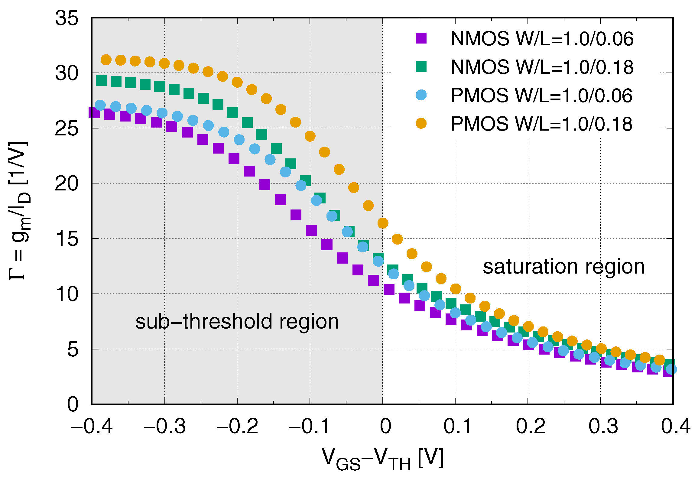
3.3. Noise Analysis and First-Stage Transconductance

Noise is expressed in terms of input equivalent noise spectral density and, as known, in multi-stage amplifiers it mainly depends on the first stage. Neglecting for simplicity the flicker noise, the general expression of the noise spectral density is:
S n , in = 2 · 4 k B T · 2 3 1 G m 1 1 + c
where k B = 13.8 · 10 24 J / K is the Boltzmann’s constant, T is the absolute temperature and c is a coefficient that depends on the topology of the first stage.
Referring to Figure 2, in our specific case, c = g m 3 , 4 / g m 1 , 2 1 where the latter approximation assumes that the current mirror M3–M4 shares the same g m / I D ratio with the differential pair, M1–M2. Solving (23) for G m 1 , we obtain the design equation:
G m 1 32 3 · k B T S n , in
that establishes the minimum first-stage transconductance on the basis of noise specifications.

3.4. Gain–Bandwidth Product and Current Dissipation

As mentioned previously, especially when the power of the IoT system is harvested from the outside, the designed circuits cannot exceed the driving capability of the power source. In low-power interface circuits, the most critical section is represented by the amplifiers used inside since they affect the power consumption significantly [1]. Therefore, the design of the OTA cannot be separated from the optimization of its power dissipation.
The overall current dissipation of the OTA can be minimized for a given GBW specification. We assume that Γ = g m / I D is a starting point for the transistors of our amplifier. Specifically, Γ is a known quantity set by the designer on the basis of the application [59], and in the ultra-low-power context, it is certainly high (i.e., Γ > 20 V 1 ).
To simplify our discussion, we assume that all the transistors in our amplifier are biased with the same Γ ; however, it is quite effortless to adapt the following analysis when different Γ are used. Referring to Figure 2, the total current required to bias the amplifier is:
I T = 2 I 1 + I 2 + 1 + 1 r I 3 = 2 + I 2 I 1 + 1 + 1 r I 3 I 1 I 1
where, as far as the current mirror ratio, r, is concerned, the higher this value is then the lower the total current is since the current in the branch M8–M9 is reduced. However, if the current in M9 is too small, the internal pole at the drain of M8 (whose resistive contribution is 1 / g m 9 ) may decrease too much and degrade the phase margin. As a rule of thumb, a good trade-off for r is between 3 and 6 and in the following, we assume this as a known parameter. Solving (25) for I 1 and substituting the result into GBW = β G m 1 / C C 1 = β Γ I 1 / C C 1 , leads to:
GBW = Γ β I T C C 1 2 + I 2 I 1 + 1 + 1 r I 3 I 1 = Γ I T C C 2 C C 1 C C 2 2 β + G m 2 β G m 1 + 1 + 1 r G m 3 β G m 1
where, for the latter expression, we considered G m i = Γ I i . Finally, using (16)–(17), we obtain:
GBW = Γ I T C C 2 2 β C C 1 C C 2 + F c C C 1 C C 2 + K ^ e 2 K ^ i C L C C 2 1 + 1 r F c C C 1 C C 2
where we defined the function:
F c C C 1 C C 2 = C C 1 C C 2 C C 1 C C 2 + K ^ e K ^ i C L C C 2 C C 1 C C 2 + C L C C 2
Since the load capacitor, C L , is specified by the application, in the proposed design strategy, we first choose C C 2 to be as small as possible but sufficiently higher than the other parasitic capacitive contributions, and then we find the ratio C C 1 / C C 2 that maximizes the GBW in (27). This latter operation can be done analytically only for C L C C 1 , C C 2 or, from a practical point of view, when C C 2 can be chosen to be at least two orders of magnitude less than C L . In this case, we can simplify F c ( C C 1 / C C 2 ) K ^ e K ^ i C C 1 / C C 2 and the solution that optimizes the GBW results:
C C 1 C C 2 K ^ e 1 + 1 r C L C C 2 2 β + K ^ e K ^ i
In any other case, the ratio C C 1 / C C 2 that maximizes the GBW has to be numerically determined from (27).

3.5. The Design Procedure in the Sub-Threshold Region

In the proposed design procedure, we assume that the power supply, V DD , the load capacitor, C L , and the feedback factor, β , are established on the basis of the specific application. Other OTA specifications, in general, concern speed requirements (given either in terms of minimum GBW or in terms of maximum settling time within a given percentage error, ϵ ) and maximum equivalent input noise. However, as we shall discuss in the following, the design steps that make use of the GBW specification are a subset of the design steps that make use of the settling-time specification. Therefore, without loss of generality, the proposed design procedure assumes that speed requirements are specified in terms of maximum settling time. As far as the noise is concerned, we shall not consider it for the moment as it will be discussed at the end of the section.
The first step in the design procedure is to choose the transistors’ bias region in terms of Γ = g m / I D . The simplest option is to choose the same Γ for all the active devices of the OTA. However, if the designer has the necessity of using different Γ for different amplification stages (or groups of transistors), the design procedure can be adapted without much effort. Clearly, in our ultra-low-power context, any value of Γ higher than 20 V 1 represents a good design choice. In this step, we also choose the secondary compensation capacitor, C C 2 , and the ratio r of the current mirror M9–M10. As discussed in Section 3.4, capacitor C C 2 has to be set as small as possible provided that, at the end of the procedure, it must result to be sufficiently higher than the other parasitic capacitive contributions. For the current mirror ratio, r, a value between 3 and 6 represents a reasonable choice.
As a second step, using (22), we evaluated the required GBW from the settling-time specifications. Obviously, if the speed requirements are already given in terms of GBW we shall use this latter value, instead.
In the third step, we have to assign a proper value to the separation factors and find the optimum ratio C C 1 / C C 2 . In the process, we must consider that setting K ^ e = 8 / 3 and K ^ i = 9 / 4 optimizes the small-signal settling time, while setting K ^ e = K ^ i = 2 optimizes the closed-loop bandwidth of the amplifier. In our specific case, C L is large (i.e., about two orders of magnitude higher than C C 2 ) and we can use the approximate Equation (29) to evaluate C C 1 / C C 2 . Otherwise, we have to use (27) to calculate numerically the ratio C C 1 / C C 2 that maximizes the GBW . Since C C 2 is known, we easily evaluate C C 1 and, subsequently:
G m 1 = C C 1 GBW β .
In the fourth step, we use (16)–(17) to evaluate the ratios G m 2 / ( β G m 1 ) and G m 3 / ( β G m 1 ) , and then, the remaining transconductances G m 2 and G m 3 . Of course, we also have G mf = G m 3 .
Finally, in the fifth step, we evaluate the stage currents from I i = G m i / Γ .
If noise specification is given, a minimum value for G m 1 is established from (24). If this minimum value is higher than that obtained from (30), the procedure shall use the transconductance value sets by the noise specification. This can be accomplished by simply evaluating the maximum between (30) and (24) in the computation of G m 1 in the third step of the procedure.
A Matlab script containing the aforementioned design procedure is reported in the Appendix A. The section ‘Specifications’ can be changed by the designer on the basis of the final application. In Section ‘Step 1’, the designer chooses the parameters gamma, CC2 and r. Similarly, in ‘Step 3’ the designer sets the separation factors, Ke and Ki. The remaining part of the script evaluates the amplifier parameters. Note that the procedure can be implemented without any advanced computational tool and that the script is provided just to summarize the steps. In addition, in contrast to those procedures based on more advanced ad hoc tools (such as that offered in [72]), a fine tuning at the circuit simulator level is in general required to finalize the design.

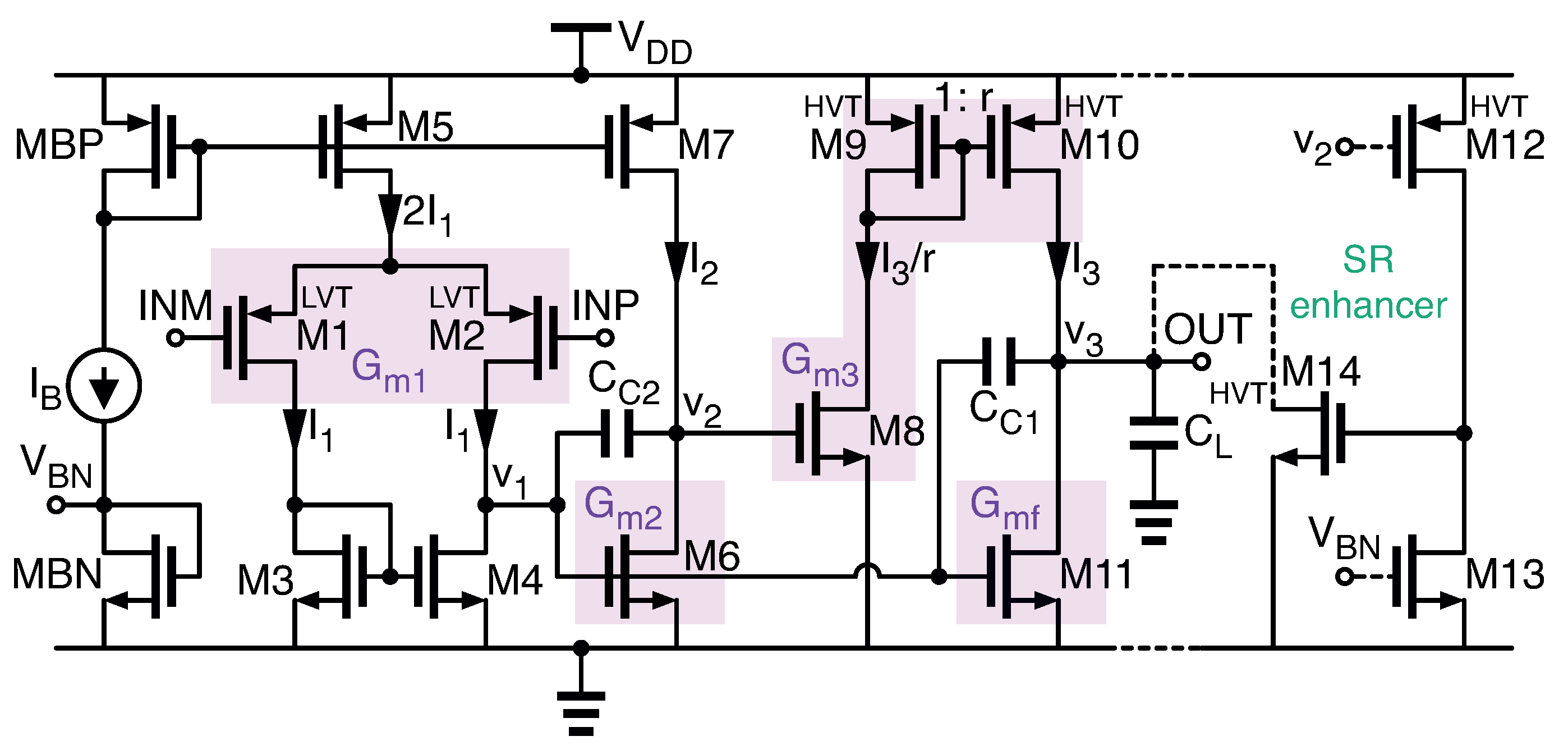
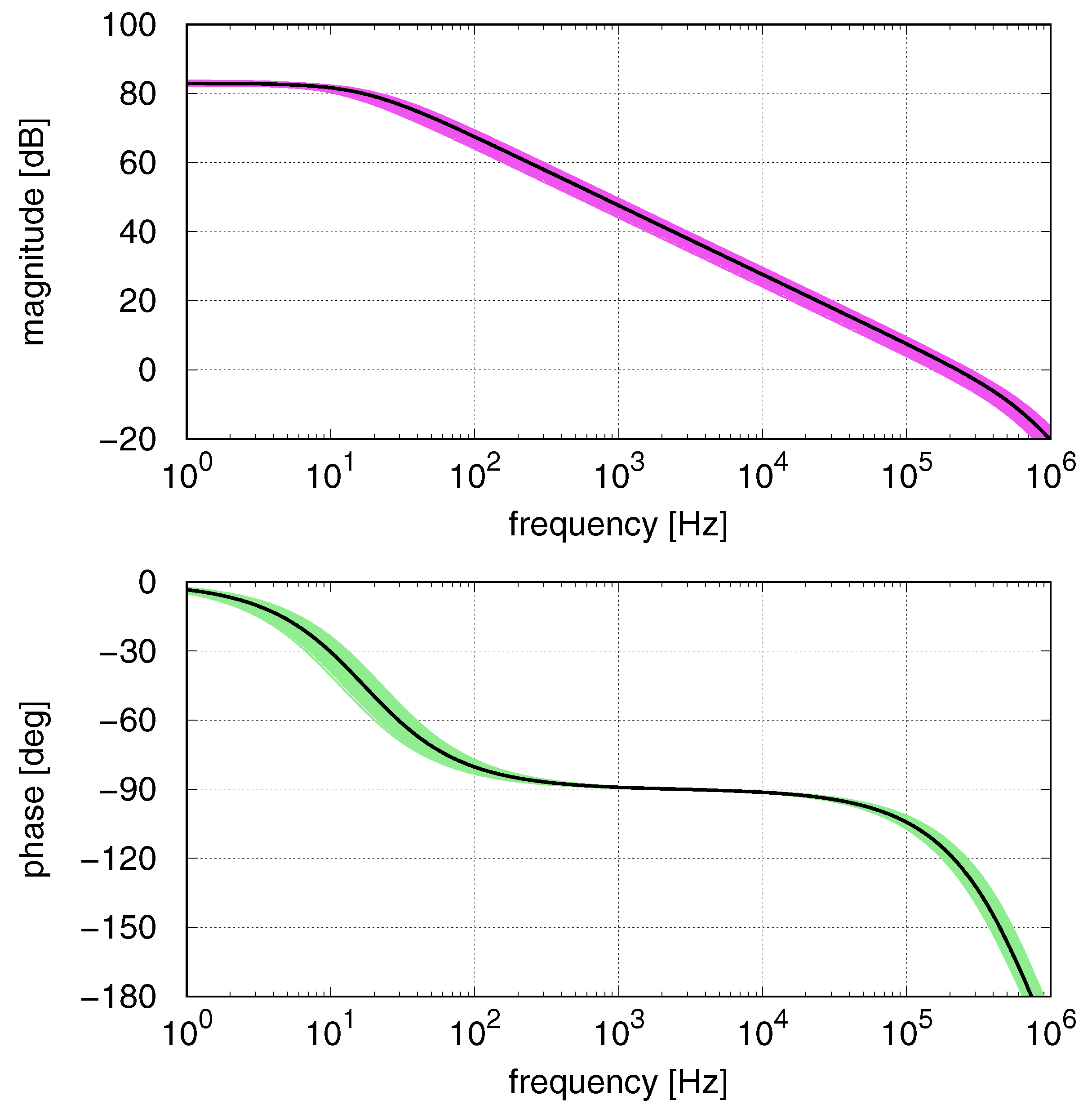
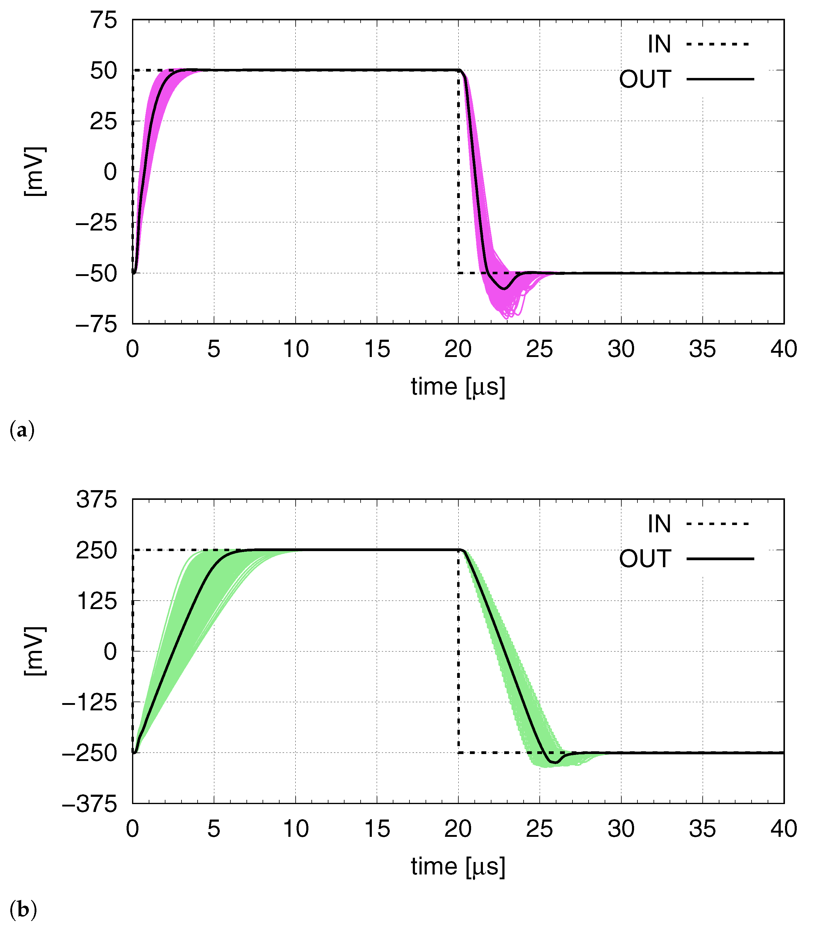
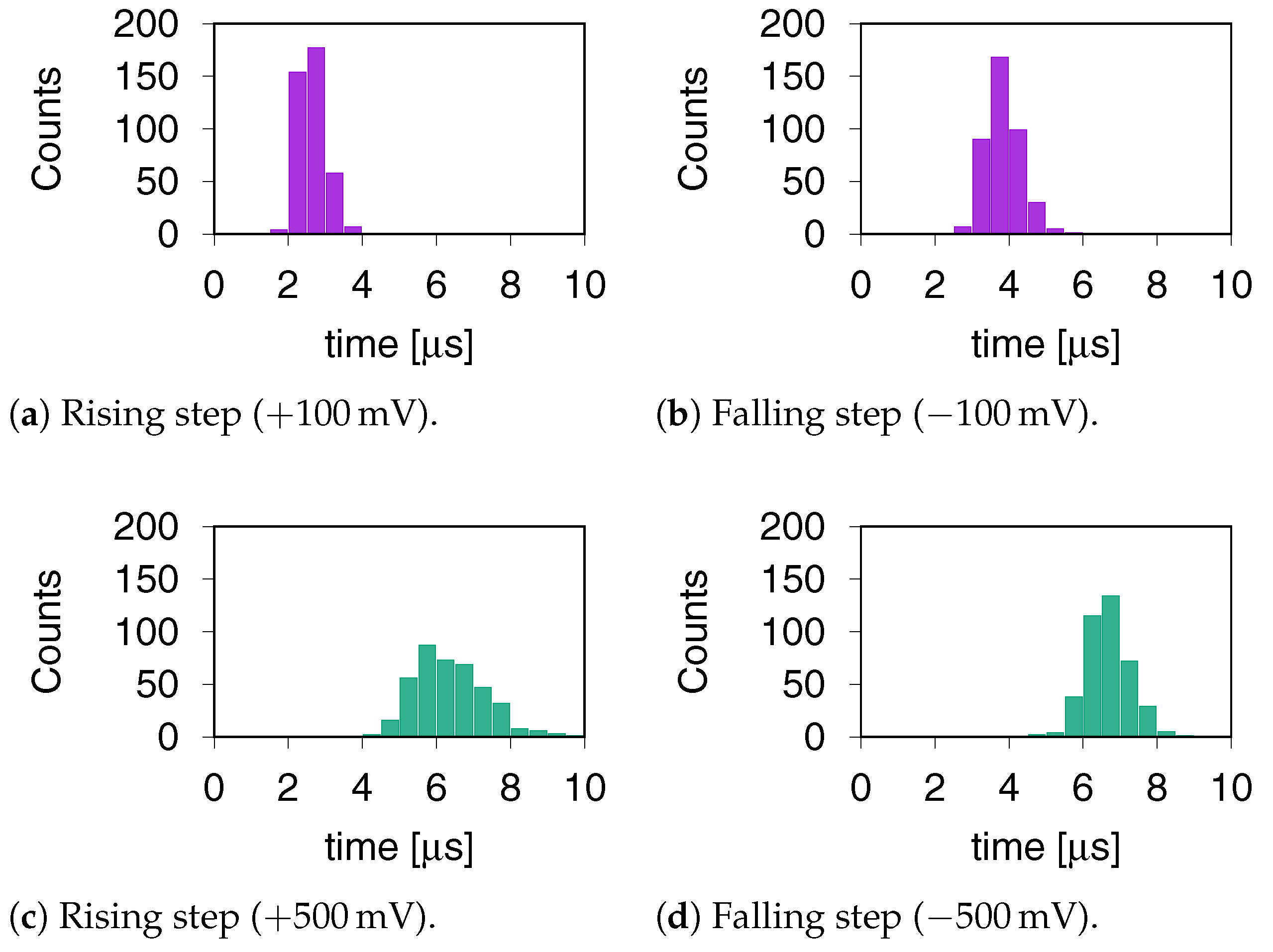
4. OTA Design and Validation Results

The three-stage OTA discussed in the previous sections is designed using a 65 nm CMOS process provided by STMicroelectronics. The power supply is set to 1 V.
As far as the specifications are concerned, the OTA is required to settle in 10 μ s within the 1-% error, when fed back in unity-gain configuration (i.e., β = 1 ) and with a load capacitor of 100 pF. These values are inserted in the Matlab script in the Appendix A. The input noise spectral density is specified as 200 nV / Hz , however, in the design, it will not play any role as it leads to a minimum transconductance smaller than that set by (30).
To improve the efficiency, we set Γ = 30 V 1 . We also set C C 2 = 150 fF , r = 4 , K ^ e = 8 / 3 and K ^ i = 9 / 4 . The design procedure leads to the OTA parameters in Table 1. With these parameters, the expected GBW is 253 kHz.
The circuit is designed in the Cadence environment following the transistor-level schematic in Figure 2. The transistors’ aspect ratios are sized according to the values in Table 1 and are reported in Table 2.
The simulated Bode plot of the open-loop gain of the OTA is shown in Figure 4 where the magnitude and the phase are depicted. The two black lines, in the magnitude graph and in the phase one come from the simulation for typical transistor models. The colored regions (violet and green, respectively) are the results of a 400-run Monte Carlo simulation that includes both intra-die (local) and inter-die (global) variations. In the format μ ± σ , the OTA exhibits a DC gain of 82.9 ± 0.24 dB , a GBW is 240 ± 27.0 kHz and a phase margin of 58.3 ± 2.8 deg .
The time response to a step input in a unity-gain configuration is reported in Figure 5. Specifically, Figure 5a shows the response to a ± 100 mV input step and Figure 5b shows the response to a ± 500 mV input step. Moreover, in these cases, the black lines come from the simulation for typical transistor models while the colored regions are the results of a 400-run Monte Carlo simulation that includes both intra-die (local) and inter-die (global) variations. In the format μ ± σ , for the ± 100 mV case, the rising step settles in 2.64 ± 0.35 μ s and the falling step in 3.84 ± 0.48 μ s . When the step increases up to ± 500 mV , slew-rate limitations slow down the OTA response that settles in 6.37 ± 0.94 μ s and in 6.68 ± 0.57 μ s for the rising and the falling step, respectively.
Finally, in Figure 6, for the various cases, we plot the distributions of the settling times that come out from the 400-run Monte Carlo simulation. The cases with ± 100 -mV steps are reported in Figure 6a,b and the cases with ± 500 mV steps are reported in Figure 6c,d. The distributions confirm again the goodness of the proposed design procedure.

Comparison with Other Recent Sub 1-V Amplifiers

A comparison with a small but significant selection of recent sub 1 V amplifiers has been carried out and the results are summarized in Table 3.
The selection includes the gate-driven and bulk-driven three-stage OTAs, where the latter group exhibits lower supply voltages. Power dissipations range from few tens of nano-Watts to few tens of micro-Watts. To have an effective comparison, the “speed” of the OTAs was measured in terms of the GBW instead of using the settling time. This is because the step response was partially characterized in some of the papers used for the comparison. The comparison was made in terms of the two well-known figures-of-merit (FOMs), defined as
IFOM s = GBW × C L I DD MHz × pF mA
FOM s = GBW × C L V DD × I DD MHz × pF mW
both measuring the goodness of the trade-off between the speed, the load capacitor and the current/power dissipation. From the last two rows of Table 3, it is apparent that the OTA designed with the proposed approach has the best performance even compared to the most recent ultra-low-voltage bulk-driven amplifiers.

5. Conclusions

In this paper we proposed a new strategy for the design of ultra-low-power CMOS OTAs, using the g m / I D approach and for the IoT scenario. The design strategy allowed to optimize the speed/dissipation in terms of settling time, including slew-rate effects. Despite the fact that procedure was cut out for large capacitive loads and for transistors biased in the sub-threshold region, it is suitable also for low-capacitive loads or for transistors biased in the saturation region. The procedure was validated through the design of the well-known three-stage RNMC-FF OTA, starting from capacitive load and settling time requirements. Simulations confirmed that the OTA satisfied the specifications (even under Monte Carlo analysis) thus proving the correctness of the proposed design strategy.

Author Contributions

Conceptualization, G.G.; formal analysis, G.G.; methodology, G.G.; resources, G.P.; supervision, G.P.; validation, G.G.; visualization, G.G.; writing—original draft, G.G.; writing—review and editing, G.P. All authors have read and agreed to the published version of the manuscript.

Funding

This work was supported in part by Università degli Studi di Catania through the Project “Programma Ricerca di Ateneo UNICT 2020-22 linea 2”.

Data Availability Statement

The data presented in this study are available on request from the corresponding author. The data are not publicly available due to the non-disclosure agreement signed with owner of the technology process.

Conflicts of Interest

The authors declare no conflict of interest.

Appendix A. MatLab Code of the Proposed Design Procedure

Jlpea 11 00021 i001

References

  1. Alioto, M. (Ed.) Enabling the Internet of Things: From Integrated Circuits to Integrated Systems; Springer: Berlin/Heisenberg, Germany, 2017. [Google Scholar] [CrossRef]
  2. Jang, T.; Kim, G.; Kempke, B.; Henry, M.B.; Chiotellis, N.; Pfeiffer, C.; Kim, D.; Kim, Y.; Foo, Z.; Kim, H.; et al. Circuit and System Designs of Ultra-Low Power Sensor Nodes With Illustration in a Miniaturized GNSS Logger for Position Tracking: Part I—Analog Circuit Techniques. IEEE Trans. Circuits Syst. I 2017, 64, 2237–2249. [Google Scholar] [CrossRef]
  3. Jang, T.; Kim, G.; Kempke, B.; Henry, M.B.; Chiotellis, N.; Pfeiffer, C.; Kim, D.; Kim, Y.; Foo, Z.; Kim, H.; et al. Circuit and System Designs of Ultra-Low Power Sensor Nodes With Illustration in a Miniaturized GNSS Logger for Position Tracking: Part II—Data Communication, Energy Harvesting, Power Management, and Digital Circuits. IEEE Trans. Circuits Syst. I 2017, 64, 2250–2262. [Google Scholar] [CrossRef]
  4. Tse, K.; Ho, B.; Chung, H.H.; Hui, S. A comparative study of maximum-power-point trackers for photovoltaic panels using switching-frequency modulation scheme. IEEE Trans. Ind. Electron. 2004, 51, 410–418. [Google Scholar] [CrossRef]
  5. Pulvirenti, F.; La Scala, A.; Ragonese, D.; D’Souza, K.; Tina, G.M.; Pennisi, S. 4-Phase Interleaved Boost Converter With IC Controller for Distributed Photovoltaic Systems. IEEE Trans. Circuits Syst. I 2013, 60, 3090–3102. [Google Scholar] [CrossRef]
  6. Abella, C.S.; Bonina, S.; Cucuccio, A.; D’Angelo, S.; Giustolisi, G.; Grasso, A.D.; Imbruglia, A.; Mauro, G.S.; Nastasi, G.A.; Palumbo, G.; et al. Autonomous Energy-efficient Wireless Sensor Network Platform for Home/Office Automation. IEEE Sens. J. 2019, 19, 3501–3512. [Google Scholar] [CrossRef]
  7. Giustolisi, G.; Palumbo, G. Dynamic-biased capacitor-free NMOS LDO. IET Electron. Lett. 2009, 45, 1140–1141. [Google Scholar] [CrossRef]
  8. Giustolisi, G.; Palumbo, G.; Spitale, E. A 50-mA 1-nF Low-Voltage Low-Dropout Voltage Regulator for SoC Applications. ETRI J. 2010, 32, 520–529. [Google Scholar] [CrossRef]
  9. Giustolisi, G.; Palumbo, G.; Spitale, E. Robust Miller Compensation with Current Amplifiers Applied to LDO Voltage Regulators. IEEE Trans. Circuits Syst. I 2012, 59, 1880–1893. [Google Scholar] [CrossRef]
  10. Grasso, A.D.; Pennisi, S. Micro-scale inductorless maximum power point tracking DC–DC converter. IET Power Electron. 2013, 6, 1634–1639. [Google Scholar] [CrossRef]
  11. Leung, K.N.; Mok, P.K.T.; Ki, W.H.; Sin, J.K.O. Three-Stage Large Capacitive Load Amplifier with Damping-Factor-Control Frequency Compensation. IEEE J. Solid State Circuits 2000, 35, 221–230. [Google Scholar] [CrossRef]
  12. Peng, X.; Sansen, W.; Hou, L.; Wang, J.; Wu, W. Impedance Adapting Compensation for Low-Power Multistage Amplifiers. IEEE J. Solid State Circuits 2011, 46, 445–451. [Google Scholar] [CrossRef]
  13. Taherzadeh-Sani, M.; Hamoui, A.A. A 1-V Process-Insensitive Current-Scalable Two-Stage Opamp With Enhanced DC Gain and Settling Behavior in 65-nm Digital CMOS. IEEE J. Solid State Circuits 2011, 46, 660–668. [Google Scholar] [CrossRef]
  14. Yan, Z.; Mak, P.-I.; Law, M.-K.; Martins, R.P. A 0.016-mm2 144-μW Three-Stage Amplifier Capable of Driving 1-to-15 nF Capacitive Load With >0.95-MHz GBW. IEEE J. Solid State Circuits 2013, 48, 527–540. [Google Scholar] [CrossRef]
  15. Tan, M.; Ki, W.-H. A Cascode Miller-Compensated Three-Stage Amplifier With Local Impedance Attenuation for Optimized Complex-Pole Control. IEEE J. Solid State Circuits 2015, 50, 440–449. [Google Scholar] [CrossRef]
  16. Centurelli, F.; Monsurrò, P.; Parisi, G.; Tommasino, P.; Trifiletti, A. A Topology of Fully Differential Class-AB Symmetrical OTA With Improved CMRR. IEEE Trans. Circuits Syst. II 2018, 65, 1504–1508. [Google Scholar] [CrossRef]
  17. Centurelli, F.; Monsurrò, P.; Parisi, G.; Tommasino, P.; Trifiletti, A. A 0.6 V class-AB rail-to-rail CMOS OTA VDD exploiting threshold lowering. IET Electron. Lett. 2018, 54, 930–932. [Google Scholar] [CrossRef]
  18. Cellucci, D.; Centurelli, F.; Di Stefano, V.; Monsurrò, P.; Pennisi, S.; Scotti, G.; Trifiletti, A. 0.6-V CMOS cascode OTA with complementary gate-driven gain-boosting and forward body bias. Int. J. Circ. Theor. Appl. 2020, 48, 15–27. [Google Scholar] [CrossRef]
  19. Blalock, B.J.; Allen, P.E.; Rincon-Mora, G.A. Designing 1-V op amps using standard digital CMOS technology. IEEE Trans. Circuits Syst. II 1998, 45, 769–780. [Google Scholar] [CrossRef] [Green Version]
  20. Stockstad, T.; Yoshizawa, H. A 0.9-V 0.5-μA rail-to-rail CMOS operational amplifier. IEEE J. Solid State Circuits 2002, 37, 286–292. [Google Scholar] [CrossRef]
  21. Ferreira, L.H.C.; Pimenta, T.C.; Moreno, R.L. An Ultra-Low-Voltage Ultra-Low-Power CMOS Miller OTA With Rail-to-Rail Input/Output Swing. IEEE Trans. Circuits Syst. II 2007, 54, 843–847. [Google Scholar] [CrossRef]
  22. Zuo, L.; Islam, S.K. Low-Voltage Bulk-Driven Operational Amplifier With Improved Transconductance. IEEE Trans. Circuits Syst. I 2013, 60, 2084–2091. [Google Scholar] [CrossRef]
  23. Lee, S.Y.; Wang, C.P.; Chu, Y.S. Low-Voltage OTA–C Filter With an Area- and Power-Efficient OTA for Biosignal Sensor Applications. IEEE Trans. Biomed. Eng. 2019, 13, 56–67. [Google Scholar] [CrossRef]
  24. Kinget, P.R. Device Mismatch and Tradeoffs in the Design of Analog Circuits. IEEE J. Solid State Circuits 2005, 40, 1212–1224. [Google Scholar] [CrossRef]
  25. Sansen, W. Minimum Power in Analog Amplifying Blocks: Presenting a Design Procedure. IEEE Solid State Circuits Mag. 2015, 7, 83–89. [Google Scholar] [CrossRef]
  26. Cabrera-Bernal, E.; Pennisi, S.; Grasso, A.D.; Torralba, A.; Gonzalez Carvajal, R. 0.7-V Three-Stage Class-AB CMOS Operational Transconductance Amplifier. IEEE Trans. Circuits Syst. I 2016, 63, 1807–1815. [Google Scholar] [CrossRef]
  27. Grasso, A.D.; Pennisi, S.; Scotti, G.; Trifiletti, A. 0.9-V Class-AB Miller OTA in 0.35- μm CMOS With Threshold-Lowered Non-Tailed Differential Pair. IEEE Trans. Circuits Syst. I 2017, 64, 1740–1747. [Google Scholar] [CrossRef]
  28. Kulej, T.; Khateb, F. A 0.3-V 98-dB Rail-to-Rail OTA in 0.18 μm CMOS. IEEE Access 2020, 8, 27459–27467. [Google Scholar] [CrossRef]
  29. Woo, K.C.; Yang, B.D. A 0.25-V Rail-to-Rail Three-Stage OTA With an Enhanced DC Gain. IEEE Trans. Circuits Syst. II 2020, 67, 1179–1183. [Google Scholar] [CrossRef]
  30. Jakusz, J.; Jendernalik, W.; Blakiewicz, G.; Kłosowski, M.; Szczepański, S. A 1-nS 1-V Sub-1-μW Linear CMOS OTA with Rail-to-Rail Input for Hz-Band Sensory Interfaces. Sensors 2020, 20, 3303. [Google Scholar] [CrossRef]
  31. Rodovalho, L.H.; Aiello, O.; Rodrigues, C.R. Ultra-Low-Voltage Inverter-Based Operational Transconductance Amplifiers with Voltage Gain Enhancement by Improved Composite Transistors. Electronics 2020, 9, 1410. [Google Scholar] [CrossRef]
  32. Manfredini, G.; Catania, A.; Benvenuti, L.; Cicalini, M.; Piotto, M.; Bruschi, P. Ultra-Low-Voltage Inverter-Based Amplifier with Novel Common-Mode Stabilization Loop. Electronics 2020, 9, 1019. [Google Scholar] [CrossRef]
  33. Toledo, P.; Crovetti, P.; Aiello, O.; Alioto, M. Fully Digital Rail-to-Rail OTA With Sub-1000-μm2 Area, 250-mV Minimum Supply, and nW Power at 150-pF Load in 180 nm. IEEE Solid State Circuits Lett. 2020, 3, 474–477. [Google Scholar] [CrossRef]
  34. Rodovalho, L.H.; Ramos Rodrigues, C.; Aiello, O. Self-Biased and Supply-Voltage Scalable Inverter-Based Operational Transconductance Amplifier with Improved Composite Transistors. Electronics 2021, 10, 935. [Google Scholar] [CrossRef]
  35. Centurelli, F.; Della Sala, R.; Monsurrò, P.; Scotti, G.; Trifiletti, A. A 0.3 V Rail-to-Rail Ultra-Low-Power OTA with Improved Bandwidth and Slew Rate. J. Low Power Electron. Appl. 2021, 11, 19. [Google Scholar] [CrossRef]
  36. Centurelli, F.; Della Sala, R.; Scotti, G.; Trifiletti, A. A 0.3 V, Rail-to-Rail, Ultralow-Power, Non-Tailed, Body-Driven, Sub-Threshold Amplifier. Appl. Sci. 2021, 11, 2528. [Google Scholar] [CrossRef]
  37. Pugliese, A.; Cappuccino, G.; Cocorullo, G. Nested Miller compensation capacitor sizing rules for fast-settling amplifier design. IET Electron. Lett. 2005, 41, 573–575. [Google Scholar] [CrossRef]
  38. Pugliese, A.; Amoroso, F.A.; Cappuccino, G.; Cocorullo, G. Settling time optimisation for two-stage CMOS amplifiers with current-buffer Miller compensation. IET Electron. Lett. 2007, 43, 1257–1258. [Google Scholar] [CrossRef]
  39. Pugliese, A.; Cappuccino, G.; Cocorullo, G. Design Procedure for Settling Time Minimization in Three-Stage Nested-Miller Amplifiers. IEEE Trans. Circuits Syst. II 2008, 55, 1–5. [Google Scholar] [CrossRef]
  40. Pugliese, A.; Amoroso, F.A.; Cappuccino, G.; Cocorullo, G. Settling Time Optimization for Three-Stage CMOS Amplifier Topologies. IEEE Trans. Circuits Syst. I 2009, 56, 2569–2582. [Google Scholar] [CrossRef]
  41. Nguyen, R.; Murmann, B. The Design of Fast-Settling Three-Stage Amplifiers Using the Open-Loop Damping Factor as a Design Parameter. IEEE Trans. Circuits Syst. I 2010, 57, 1244–1254. [Google Scholar] [CrossRef]
  42. Yang, Y.; Binkley, D.M.; Li, C. Using Moderate Inversion to Optimize Voltage Gain, Thermal Noise, and Settling Time in Two-stage CMOS Amplifiers. In Proceedings of the IEEE ISCAS 2012, Seoul, Korea, 20–23 May 2012; pp. 432–435. [Google Scholar] [CrossRef]
  43. Seth, S.; Murmann, B. Settling Time and Noise Optimization of a Three-Stage Operational Transconductance Amplifier. IEEE Trans. Circuits Syst. I 2013, 60, 1168–1174. [Google Scholar] [CrossRef]
  44. Giustolisi, G.; Palumbo, G. Compensation strategy for high-speed three-stage switched-capacitor amplifiers. IET Electron. Lett. 2016, 52, 1202–1204. [Google Scholar] [CrossRef]
  45. Giustolisi, G.; Palumbo, G. Robust design of CMOS amplifiers oriented to datasettime specification. Int. J. Circ. Theor. Appl. 2017, 45, 1329–1348. [Google Scholar] [CrossRef]
  46. Prasopsin, P.; Wattanapanitch, W. A Sub-Microwatt Class-AB Super Buffer: Frequency Compensation for datasetTime Improvement. IEEE Trans. Circuits Syst. II 2018, 65, 26–30. [Google Scholar] [CrossRef]
  47. Giustolisi, G.; Palumbo, G. Bessel-like compensation of three-stage operational transconductance amplifiers. Int. J. Circ. Theor. Appl. 2018, 46, 729–747. [Google Scholar] [CrossRef]
  48. Lavalle-Aviles, F.; Torres, J.; Sánchez-Sinencio, E. A High Power Supply Rejection and Fast Settling Time Capacitor-Less LDO. IEEE Trans. Power Electron. 2019, 34, 474–484. [Google Scholar] [CrossRef]
  49. Mandal, D.; Desai, C.; Bakkaloglu, B.; Kiaei, S. Adaptively Biased Output Cap-Less NMOS LDO With 19 ns Settling Time. IEEE Trans. Circuits Syst. II 2019, 66, 167–171. [Google Scholar] [CrossRef]
  50. Grasso, A.D.; Palumbo, G.; Pennisi, S. Analytical comparison of frequency compensation techniques in three-stage amplifiers. Int. J. Circ. Theor. Appl. 2008, 36, 53–80. [Google Scholar] [CrossRef]
  51. Grasso, A.D.; Marano, D.; Palumbo, G.; Pennisi, S. Analytical comparison of reversed nested Miller frequency compensation techniques. Int. J. Circ. Theor. Appl. 2010, 38, 709–737. [Google Scholar] [CrossRef]
  52. Silveira, F.; Flandre, D.; Jespers, P.G.A. A gm/ID based methodology for the design of CMOS analog circuits and its application to the synthesis of a silicon-on-insulator micropower OTA. IEEE J. Solid State Circuits 1996, 31, 1314–1319. [Google Scholar] [CrossRef]
  53. Flandre, D.; Viviani, A.; Eggermont, J.P.; Gentinne, B.; Jespers, P.G.A. Improved synthesis of gain-boosted regulated-cascode CMOS stages using symbolic analysis and gm/ID methodology. IEEE J. Solid State Circuits 1997, 32, 1006–1012. [Google Scholar] [CrossRef]
  54. Jespers, P.G.A.; Murmann, B. Systematic Design of Analog CMOS Circuits Using Pre-Computed Lookup Tables; Cambridge University Press: Cambridge, UK, 2017. [Google Scholar] [CrossRef]
  55. Murmann, B. gm/ID Starter Kit. Available online: https://web.stanford.edu/~murmann/gmid (accessed on 11 May 2021).
  56. Sabry, M.N.; Omran, H.; Dessouky, M. Systematic design and optimization of operational transconductance amplifier using gm/ID design methodology. Microelectron. J. 2018, 75, 87–96. [Google Scholar] [CrossRef]
  57. Aminzadeh, H. Systematic circuit design and analysis using generalised gm/ID functions of MOS devices. IET Circuits Devices Syst. 2020, 14, 432–443. [Google Scholar] [CrossRef]
  58. Youssef, A.A.; Murmann, B.; Omran, H. Analog IC Design Using Precomputed Lookup Tables: Challenges and Solutions. IEEE Access 2020, 8, 134640–134652. [Google Scholar] [CrossRef]
  59. Kinget, P.R. Scaling analog circuits into deep nanoscale CMOS: Obstacles and ways to overcome them. In Proceedings of the IEEE CICC 2015, San Jose, CA, USA, 28–30 September 2015; pp. 1–8. [Google Scholar] [CrossRef]
  60. Giustolisi, G.; Palumbo, G. Design of Three-Stage OTA Based on datasetTime Requirements Including Large and Small Signal Behavior. IEEE Trans. Circuits Syst. I 2021, 68, 998–1011. [Google Scholar] [CrossRef]
  61. Giustolisi, G.; Palumbo, G. Design of CMOS three-stage amplifiers for near-to-minimum datasettime. Microelectron. J. 2021, 107. [Google Scholar] [CrossRef]
  62. Giustolisi, G.; Palumbo, G. Efficient Design Strategy for Optimizing the Settling Time in Three-Stage Amplifiers Including Small- and Large-Signal Behavior. Electronics 2021, 10, 612. [Google Scholar] [CrossRef]
  63. Giustolisi, G.; Palumbo, G. In-depth Analysis of Pole-Zero Compensations in CMOS Operational Transconductance Amplifiers. IEEE Trans. Circuits Syst. I 2019, 66, 4557–4570. [Google Scholar] [CrossRef]
  64. Yavari, M.; Maghari, N.; Shoaei, O. An Accurate Analysis of Slew Rate for Two-Stage CMOS Opamps. IEEE Trans. Circuits Syst. II 2005, 52, 164–167. [Google Scholar] [CrossRef]
  65. Marano, D.; Palumbo, G.; Pennisi, S. Step-response optimisation techniques for low-power, high-load, three-stage operational amplifiers driving large capacitive loads. IET Circuits Devices Syst. 2010, 4, 87–98. [Google Scholar] [CrossRef]
  66. Grasso, A.D.; Palumbo, G.; Pennisi, S. High-Performance Four-Stage CMOS OTA Suitable for Large Capacitive Loads. IEEE Trans. Circuits Syst. I 2015, 62, 2476–2484. [Google Scholar] [CrossRef]
  67. Grasso, A.D.; Marano, D.; Palumbo, G.; Pennisi, S. Design Methodology of Subthreshold Three-Stage CMOS OTAs Suitable for Ultra-Low-Power Low-Area and High Driving Capability. IEEE Trans. Circuits Syst. I 2015, 62, 1453–1462. [Google Scholar] [CrossRef]
  68. Grasso, A.D.; Marano, D.; Palumbo, G.; Pennisi, S. High-Performance Three-Stage Single-Miller CMOS OTA With No Upper Limit of CL. IEEE Trans. Circuits Syst. II 2018, 65, 1529–1533. [Google Scholar] [CrossRef]
  69. Giustolisi, G.; Grasso, A.D.; Pennisi, S. High-Drive and Linear CMOS Class-AB Pseudo-Differential Amplifier. IEEE Trans. Circuits Syst. II 2007, 54, 112–116. [Google Scholar] [CrossRef]
  70. Giustolisi, G.; Palumbo, G. Three-Stage Dynamic-Biased CMOS Amplifier With a Robust Optimization of the Settling Time. IEEE Trans. Circuits Syst. I 2015, 62, 2641–2651. [Google Scholar] [CrossRef]
  71. Giustolisi, G.; Palumbo, G.; Pennisi, S. Class-AB CMOS output stages suitable for low-voltage amplifiers in nanometer technologies. Microelectron. J. 2019, 92, 104597. [Google Scholar] [CrossRef]
  72. Master Micro Analog IC Design. Available online: http://www.master-micro.com/mastering-microelectronics/courses/analog-ic-design (accessed on 11 May 2021).
Figure 1. Block schematic of the three-stage OTA based on the reverse nested Miller compensation with feed-forward stage (RNMC-FF).
Jlpea 11 00021 g001
Figure 2. The transistor-level implementation of the three-stage OTA based on the reverse nested Miller compensation with feed-forward stage (RNMC-FF).
Jlpea 11 00021 g002
Figure 3. g m / I D ratio vs. the gate–source overdrive, V G S V TH , for the 65 nm regular threshold transistors. The plots are produced for two different channel lengths and for both the complementary devices. The plot puts into evidence the sub-threshold region and the saturation one. W and L are expressed in microns.
Jlpea 11 00021 g003
Figure 4. Bode plot of the open-loop gain of the OTA (magnitude and phase). Black lines: transistor typical models. Colored lines: 400-run Monte Carlo simulation with intra-die (local) and inter-die (global) variations.
Jlpea 11 00021 g004
Figure 5. Time response to step input signals. Black lines: transistor typical models. Colored lines: 400-run Monte Carlo simulation with intra-die (local) and inter-die (global) variations. (a) Input step of ± 100 mV ; (b) Input step of ± 500 mV .
Jlpea 11 00021 g005
Figure 6. Monte-Carlo simulation of the settling time of the closed-loop OTA compensated with the RNMC-FF.
Jlpea 11 00021 g006
Table 1. OTA parameters: results from the design procedure.
ParameterValue
G m 1 3.97 μ A / V
G m 2 23.4 μ A / V
G m 3 26.0 μ A / V
G mf 26.0 μ A / V
I 1 132 nA
I 2 779 nA
I 3 865 nA
C C 1 2.5 pF
C C 2 150 fF
Table 2. Transistors’ aspect ratios of the OTA (W and L are expressed in microns).
TransistorAspect Ratio
M1 *, M2 * 10 / 0.25
M3, M4 3 / 0.25
M5 6 / 0.5
M6 18 / 0.25
M7 16.5 / 0.5
M8 4.5 / 0.25
M9 6 / 0.25
M10 24 / 0.25
M11 18 / 0.25
M12 0.5 / 8
M13 10 / 0.5
M14 1 / 1
MBN 5 / 0.5
MBP 3 / 0.5
* Low-threshold transistor; † High-threshold transistor.
Table 3. Performance comparison of sub 1 V Amplifiers.
[26][27][28][29]This Work
Tech180 nm350 nm180 nm65 nm65 nm
Year20162017202020202021
Input-drivenBulkGateBulkBulkGate
V DD (V)0.70.90.30.251.0
I DD ( μ A)36.327.00.0430.1042.12
Power ( μ W)25.424.30.0130.0262.12
C L (pF)20103015100
GBW (kHz)300010003.19.5253
IFOM s 16533702146137011,934
FOM s 23614127154548111,934
Publisher’s Note: MDPI stays neutral with regard to jurisdictional claims in published maps and institutional affiliations.

