Review

Adaptative Techniques to Reduce Power in Digital Circuits

1
ECE Department, Indian Institute of Science/Bangalore 560012, India
2
Texas Instruments/Bangalore 560012, India
*
Author to whom correspondence should be addressed.
J. Low Power Electron. Appl. 2011, 1(2), 261-276; https://doi.org/10.3390/jlpea1020261
Submission received: 23 November 2010 / Revised: 13 June 2011 / Accepted: 21 June 2011 / Published: 4 July 2011
(This article belongs to the Special Issue Selected Topics in Low Power Design - From Circuits to Applications)

Abstract

:
CMOS chips are engineered with sufficient performance margins to ensure that they meet the target performance under worst case operating conditions. Consequently, excess power is consumed for most cases when the operating conditions are more benign. This article will review a suite of dynamic power minimization techniques, which have been recently developed to reduce power consumption based on actual operating conditions. We will discuss commonly used techniques like Dynamic Power Switching (DPS), Dynamic Voltage and Frequency Scaling (DVS and DVFS) and Adaptive Voltage Scaling (AVS). Recent efforts to extend these to cover threshold voltage adaptation via Dynamic Voltage and Threshold Scaling (DVTS) will also be presented. Computation rate is also adapted to actual work load requirements via dynamically changing the hardware parallelism or by controlling the number of operations performed. These will be explained with some examples from the application domains of media and wireless signal processing.

1. Introduction

Power dissipation in a digital CMOS chip is given as:
P = N a ( a C V D D 2 f + I l e a k , a V D D ) + N i I l e a k , i V D D
where Na and Ni are the total number of gates in active and asleep logic blocks respectively, a is the activity factor, C is the average capacitance of the net associated with the output of a gate, f is the operation frequency, and VDD is the supply voltage. Ileak,a and Ileak,i are the leakage currents per gate of active and asleep logic blocks respectively. For the active logic blocks, the first term within brackets is the dynamic power due to the capacitances charging and discharging and the second term is the leakage power of all the cells connected to the power supply. The asleep logic blocks are disconnected from the power supply to substantially reduce their leakage currents Ileak,i, as compared to Ileak,a.
Typically, the chip is designed to accommodate the peak computation requirements, even under the worst case process and temperature conditions. The peak computation throughput in combination with the architecture (the types of macro blocks like processing cores and memories and their interconnection scheme) and the micro-architecture (cycle level pipelining and parallelism) determines the peak operating frequency, f. The physical design of the chip with actual gate choices, their placement and wiring layout, is done to meet the frequency f at worst case process and temperature conditions. This finally determines the total number of gates (and memory cells), the switching capacitances (from gate sizes and wiring parasitics), the leakage currents and the supply voltage VDD in Equation 1. The activity factor, a, is largely determined by the situation at run-time, i.e., on the kinds of computation being done and the actual data that is being worked on.
There has been intense research over the past two decades on various aspects of compilation and synthesis for low power [1]. Many architectural optimizations like re-configurable architectures, custom ASIC approaches, programmable multi-cores, etc. have been explored. Micro-architectural techniques like parallelism and pipelining, power and clock gating have become commonplace now. Circuit techniques for low voltage operation, standby current reduction, optimal gate sizing have also been explored and are available for use by a designer [2].
Most of these optimization techniques are static techniques which are applied during design time. In the recent past, dynamic power management techniques have emerged, where the power consumption is continuously adjusted during run time of the system [3,4]. This is motivated by the fact that since the chip is designed to meet the most demanding application throughput requirements under worst case operating condition, it leads to an excess margin or wastage of power under typical operating conditions. In the next section, we will review some commonly used techniques like dynamic power switching and dynamic and adaptive voltage scaling. We will also describe some recent research in dynamic voltage and threshold scaling. We will then discuss techniques which have been recently explored to adapt to varying computation needs via adapting the hardware parallelism or changing the number of operations performed dynamically.

2. Dynamic Power Management

Figure 1 shows the set of dynamic power management techniques, which have become quite common in modern low power chips. These techniques are used during chip operation to continually adjust the power consumption based on the dynamically varying operating requirements.

2.1. Dynamic Power Switching

From 90 nm process node onwards, leakage currents have substantially gone up with as much as 30% of the total active power being contributed by the leakage power alone. This has led to the development of the power switching technique, wherein the unused logic blocks are disconnected from the power supply via a CMOS switch [5].
Figure 2a shows the basic idea of power switching, which consists of an additional series PMOS device connecting the internal power supply node of the IP block to the on-chip power distribution grid. The PMOS power switch is sized carefully to limit the performance loss to be less than 10% [6]. During long inactive periods, the IP block is disconnected from the supply by turning OFF the PMOS switch. This reduces the leakage current by up to 40× when compared to active mode [4]. Special attention has to be paid to the interfaces of the IP block as well as the internal state elements. Once the IP block is disconnected from the supply, the voltages on its nodes will be very poorly controlled and hence need to be isolated from the external blocks. Special, low leakage retention latches are used to store state when the IP block is disconnected from the supply [7]. The state is automatically restored upon connection back to the power supply. As an example, in a recent mobile application processor SoC only the memory and the MP3 decoder logic are kept active during MP3 audio playback, while the rest of the SoC is disconnected from the supply [4].
This idea has also been extended to SRAM blocks with a small modification (Figure 2b). An additional NMOS switch along with a parallel diode connected NMOS transistor is inserted between the SRAM macro and the ground line [4]. During standby periods, where data retention is required, the NMOS switch is disabled which leads to the virtual ground node slowly charging up to a value slightly above the threshold voltage of the NMOS diode transistor. This reduces the leakage in the SRAM array by a factor of 3×. During sleep mode, when data retention is not required, the power switch can be turned off, further reducing leakage power.

2.2. Dynamic Frequency and Voltage Scaling

2.2.1. Dynamic Frequency Scaling (DFS)

Due to the large range of the performance requirements of different applications, the concept of dynamic frequency scaling (DFS), has been developed to optimize the frequency of operation and hence power (Equation 1) [8]. For example, the needs of a video codec are orders of magnitude more than that of an audio codec. Hence the frequency of operation is adjusted as required by the application, thus reducing dynamic power.
A convenient way to adjust frequency is to use a divided version of the master clock. The advantage of this approach is that the new frequency can be obtained in just one clock cycle and hence is the fastest possible way to adjust frequency. However, this leads to large gaps in frequency values, especially between the fundamental and the first divided value.. An alternative is to adjust the divider ratio in the clock generation PLL, so that frequency can be adjusted in steps of the reference clock frequency, or even lower. However the PLL loop bandwidths are typically made small, in the MHz range, to obtain a low clock jitter. Thus the time taken to settle to a new frequency can be in the order of microseconds. Figure 3 shows another technique, using clock dividers and a state machine, to obtain much finer resolution frequency control, but with very low latency to change the frequency [8]. It is based on the observation that the clock does not have to be periodic. Hence the approach uses the next lowest frequency octave and selectively suppresses the required number of clock edges to obtain the desired frequency value. For example, the system generates clocks of frequency 128 MHz, 96 MHz, 64 MHz, 48 MHz, 32 MHz, 16 MHz and 8 MHz via a simple divider. Any frequency between 8 and 128 MHz in steps of 1 MHz can be generated with the help of the state machine. For example, to generate 28 MHz, a 32 MHz base clock is chosen and the state machine suppresses 4 edges, in a sequence of 32 edges, to generate the desired frequency. In order to ensure a glitch free clock, the multiplexer select and enable signals are triggered at negative edges so that they are stable by the time of the positive clock edge. While this approach leads to a simple and quick way of changing frequency in small steps, it suffers from excess power dissipation compared to PLL adjustment approach as the supply voltage needs to be that for the highest base frequency used as input to the clock edge suppression state machine.

2.2.2. Dynamic Voltage Scaling (DVS)

While reducing frequency helps to reduce power, further energy efficiency gains can be obtained by also reducing the supply voltage. Equation 2 below shows the relationship between the frequency (inverse of the delay of the critical path) and the supply voltage for a super-threshold operation [9].
f = K L D ( V D D - V T H ) α C V D D
Here LD is the logic depth of the critical path, α is the velocity saturation factor, K captures process related information like mobility, oxide thickness, etc. and has temperature dependence, C is the average switching capacitance in the critical path and VTH is the threshold voltage. Thus, under DVS, for a reduced operating frequency, the supply voltage is correspondingly scaled to reduce both the power as well as the energy per operation, which is not achieved with just DFS [10].
The relationship between frequency and minimum supply voltage can be precisely captured in a table for a few frequency points, to guarantee that circuit timing is met even for the worst case process and temperature conditions. When the operating frequency is changed, the table is consulted for the appropriate supply voltage value and the voltage regulators are programmed to deliver this voltage to the chip. This is the approach currently used in many commercial chips which support DVS [4]. The timescales over which dynamic voltage changes happen is largely determined by the response time of the voltage regulators, which is in the micro-second range. Care must be taken to properly sequence the changes in frequency and voltage to always guarantee correct operation [4,7].
Note that the supply voltage chosen ensures that the chip will operate at the target frequency, under all relevant process and temperature conditions. Critical path delays can vary by a factor of 2× across slow to fast process conditions for the same supply voltage, leading to excess power loss when only one frequency-voltage relationship is used for DVS.

2.2.3. Adaptive Voltage Scaling (AVS)

Adaptive voltage scaling improves upon DVS by removing the excess margins prevalent in using a fixed voltage-frequency (V-F) relationship. It uses a V-F relationship which is adaptive to the operating conditions of the chip. The chip's exact process corner is determined either during manufacturing test or at runtime and the appropriate V-F relationship is used during DVS operation [4]. Recently AVS has been applied for a per-core voltage control in a large multi-core chip [11]. This is to account for large within-die process variations in sub-45 nm process nodes.
One commonly used approach to monitor the chip's operating condition is to use a ring oscillator operating off the same supply voltage as the rest of the chip. The ring oscillator's frequency is then indicative of the V-F relationship for the chip at that particular temperature.
Another approach to determine the per-chip V-F relationship is to use a critical path monitor, which attempts to model the critical path of the chip [8]. Figure 4 shows one such scheme where a configurable delay chain is used to model the chip's critical path [8]. The delay chain consists of chain of inverters, NAND2 gates, wire segments, etc., and the output can be tapped from one of many points, thus allowing tuning of the delay to match chip's critical path.
This exact setting of the delay chain is determined once during manufacturing test. During AVS operation, the delay is measured by launching an edge at the start of the clock cycle and then capturing the edge at the end of the clock cycle at the output of the delay chain and a set of buffers. Exact position of the rising edge is determined by analyzing the captured buffer outputs. The AVS feedback system then continually adjusts the supply voltage such that the launched rising edge makes it to a specified buffer stage—which ensures that the delay chain and hence the chip's critical path meet timing with adequate operating margins.
The main drawback of this approach is that, one still needs to provide for sufficient margins between the critical path monitor and the actual critical paths of the chip due to large within-die process variations. Additionally, the delay monitor's configuration might have to be changed for different operating voltages, due to the different scaling of interconnect and gate delays with supply voltage.
In order to overcome these limitations and further eliminate margins, the concept of RAZOR has been proposed [12]. This approach is potentially applicable for designs when further re-pipelining is not beneficial due to architectural considerations. An example is the single cycle loop, involving execute stages and bypass forwarding paths in a micro processor. Fixing any timing violations in these pipe stages for worst case conditions via additional pipelining, leads to a large degradation in the over all execution time of a program. Instead in the RAZOR technique, the delay violations in actual critical paths in a microprocessor are monitored via error detection circuity. The supply voltage is scaled down up to a point of some target error rate in these critical paths. Most microprocessors already have mechanisms to recover from wrong computations due to speculative execution. These are modified to also handle recovery from critical path timing errors to ensure that the overall computation is error free.

2.2.4. Dynamic Voltage and Threshold Scaling (DVTS)

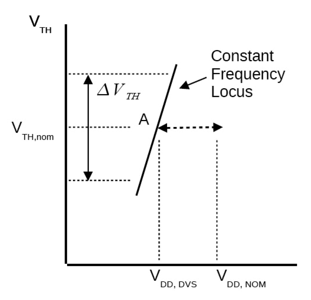
The energy efficiencies provided by DVS/AVS can be further improved by adjusting the threshold voltage in addition to the supply voltage [9]. From Equation 2, it is apparent that a constant performance can be obtained by scaling the numerator and the denominator in an identical fashion. Thus the locus of constant performance is approximately a straight line, in the VDDVTH plane as shown in Figure 5.
The DVS technique, drives down supply voltage to point A on the constant performance curve, which is at the intersection of the nominal VTH line with the constant performance locus. However, the point of minimum total power can be elsewhere on this locus and its exact location depends on the ratio of the leakage power to the dynamic power. For instance, when leakage power dominates, it is more optimal to increase threshold voltage to reduce leakage power, and increase supply voltage (and dynamic power) to maintain performance. Conversely, when dynamic power dominates, it is beneficial to reduce supply voltage and also the threshold voltage. Using simple models for power and performance, analytical results for the optimum power point have been derived [9]. Figure 6 shows power savings of DVTS over that of DVS for a 27 stage ring oscillator with 1% switching activity in a UMC 90 nm process node. The power savings of using DVTS over DVS become larger with increasing contribution of sub-threshold leakage power to total power consumption.
The threshold voltage can be controlled by changing the body bias of the transistors and is called the adaptive body bias (ABB) technique. For fast silicon, reverse body bias is applied to increase threshold and reduce leakage, while for slow silicon, forward body bias is applied to reduce threshold and improve performance [4]. Here the body bias adjustment is done sparingly as needed based on the chip's process condition, and is not a continuous variable like the supply voltage.
However the point of minimum power depends on the ratio of dynamic to leakage power, with the former modulated by the activity factor. For media applications, the activity factor can vary a lot across different applications and hence, the optimal settings for threshold and supply also vary [13]. Analogous to table based DVS, a table based DVTS scheme has been proposed where for different activity factors, the corresponding supply and body bias values are stored in the look up table. The activity factors are estimated for different applications off-line. During run-time, based on the application being run, the appropriate activity factor is used to consult the look up table to obtain the settings for supply and body bias, which will minimize power [13].
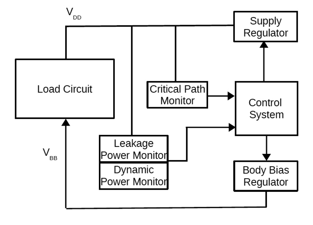
Adaptive voltage and threshold scaling aims to arrive at the optimal voltage and threshold values at run time, by not only adapting to the process and temperature like in AVS, but also to the dynamically varying activity conditions. One approach to doing this is shown in Figure 7 [14].
The critical path monitor, a control system and the supply voltage regulator are common with an AVS system. In addition, the DVTS system has a power monitor (both dynamic and leakage power) as well as a regulator to generate the body bias voltage. The control system is enhanced now to include readings from the power monitor and hunts for the optimal supply and body bias voltage which minimizes power while meeting target frequency. Dynamic and leakage power are monitored on replica circuits, much like the replica delay path. So it is essential to tune the replica circuits to match with the characteristics of the load circuit, across different process, temperature and activity conditions.
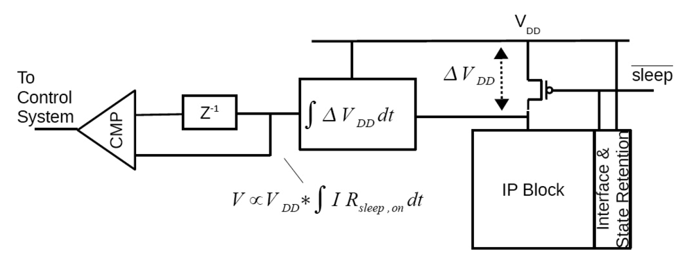
Figure 8 shows an alternative approach to monitor the total power of the load circuit.
Here the power of the logic block is directly measured by monitoring the voltage across the sleep transistor [15]. This voltage is related to the logic block's current consumption as I × Rsleep,on, where the Rsleep,on is the resistance of the power gating transistor when it is ON. An additional multiplication with VDD is achieved by making the integration time proportional to the supply voltage. This in-situ monitoring approach ensures that the power measurements are accurate across process and temperature conditions and can track the changes in activity easily. The monitoring circuit consists of an integrator, a capacitor to store monitored value of the previous step in an analog form and a comparator. The difference of the measured power in the current control loop step with respect to that from the previous step is quantized into two bits. The difference power information is used by the control system to continually adjust the VDD, VBB values to drive the system to the point of optimal power. The system can track activity changes as long as they occur at a rate less than the loop bandwidth. Simulated power savings of up to 42% is observed in a 90 nm triple well process node.
The main short coming of the DVTS technique is related to the ineffectiveness of body bias control on the threshold voltage in deep sub-micron processes. In order to limit the diode leakage currents through diffusion-body interface, the body bias voltage has to be limited to a value of ±500 mV around the nominal. With a body effect coefficient of less than 0.1, this leads to a threshold voltage modulation of less than ±50 mV, leaving very little range for adaptation.

3. Adaptive Computation

The previous section dealt with changing the computation throughput purely by changing the frequency and correspondingly the supply voltage. In this section we will look at techniques which adapt computation rate by other means like adapting the amount of hardware parallelism, or by changing the number of computation steps carried out. Note that these are orthogonal to voltage scaling and both can be combined for optimum power dissipation.

3.1. Adaptive Hardware Usage

Coarse grain hardware parallelism adaptation has been explored by many researchers and works well in a multi-core chip. The authors in a multiprocessing video decoder chip use different numbers of processing engines for different levels of video decoding performance [16]. For example, only two processing engines are used to decode a baseline H.264 video at 320 × 240 resolution and 15 frames per second with 70 mW power consumption. On the other hand, 8 engines are used to decode 854 × 480 resolution video at 30 frames per second with 315 mW of power. In this example, the computation work load requirement is easy to determine as it is based on the application being run.
Much finer grained control of the hardware has been explored by Chandrakasan et al. where they adapt the filter order and hence filter length based on the measured out of band energy [17]. The idea here is that if the input signal's out of band energy is small, then the filter transition doesn't need to be that sharp and the filter order and hence length can be reduced. The filter length can be reduced by either zeroing out the data going into the filter arms, thus eliminating data transitions and dynamic power. Alternatively, the associated filter taps and components can be powered down.
In another work, the authors adjust the precision required for filtering based on analyzing the sign extension bits of the incoming samples [18]. If out of 16-bits the top 7 bits are sign extension bits, of all the samples, then only the lower 10 bits need to be considered for the filtering. The filter is implemented using the distributed arithmetic technique, which is very amenable to variable precision arithmetic.
Adaptive word length control is used to implement an OFDM based low power wireless baseband processing system for a radio receiver [19]. OFDM processing essentially consists of filtering, followed by an FFT engine and then an equalization block. The Error Vector Magnitude (EVM) of the received signal is continuously monitored, to adjust the word length. If EVM is above a threshold, the word length is increased to improve precision and conversely, for good EVM (low error rate), the word length is reduced.
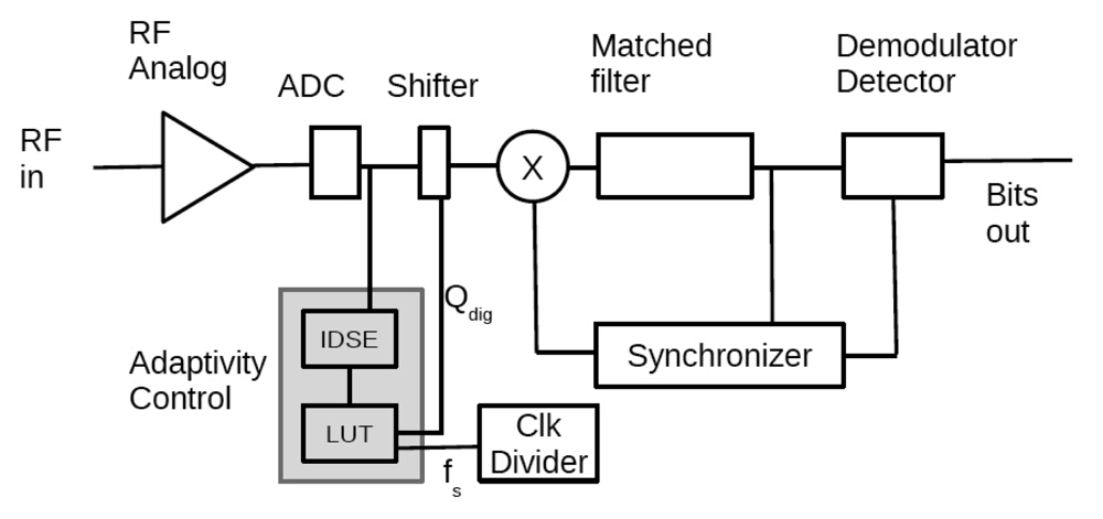
Along similar lines, the signal to noise ratio (SNR) in the received channel and the interference levels in adjacent and alternate channels are monitored in the base band digital signal processing system for a IEEE 803.15.4 radio receiver [20]. The power levels in these neighboring bands are used to adjust the sampling and operation rate in the DSP core. A high rate is used to mitigate degradation based on aliasing only when the power in the neighboring bands is high. This rate and word length adjustment is done on a packet by packet basis to achieve a fine grain adaptation of the power dissipation. Figure 9 shows the block diagram of such an adaptive receiver. It allows for control of the word length (Qdig) and sampling rate (fs). Qdig can be one of 1, 2, 4 or 8 bits and fs can be one of 2, 3, 5, 6, 10, 15 or 30 MHz. Word length is reduced by shifting the MSBs to the LSBs (by sign extending) as desired. For example for a 2-bit resolution, an 8-bit value is right shifted by 6 bits and then fed into the data path. This ensures that no switching activity occurs in the higher order bits, and hence reduces the dynamic power consumption for these bits. Variable frequency values are obtained by using a simple clock divider, which runs at 30 MHz. The chosen frequency values are obtained easily from the divider as these are factors of 30. An interference detection and signal estimation (IDSE) unit measures the interferences in the adjacent and alternate signal bands, and also estimates the signal energy. These values are used to index a look up table which determines the resolution and sampling rate for the data path which will guarantee the target bit error rate. The look up table is obtained from receiver simulations and power analysis to ensure that the least power settings, which will ensure bit error rate are entered into the table.
Prior to reception of a packet, the digital data path is set to operate at the highest resolution of 8-bits and 30 MHz. During packet preamble, in parallel with timing acquisition, the IDSE block estimates the signal and interference conditions and determines the optimal Qdig and fs settings. At the end of the preamble, the datapath's settings are adjusted to this new value so that the rest of the data symbols in the packet are received with this optimal setting for the receiver. A slice of the look up table is shown in Table 1 for two different interference and signal conditions (high and low values). It shows significant power differences between the best case and worst case input signal conditions.

3.2. Adapting the Number of Operations

The number and nature of low level operations can also be adapted dynamically to optimize power consumption. As an example, in a video encoder application, the number of computations for motion estimation is adapted for each macro-block [21]. Motion estimation is performed by comparing a macro-block with all macro-blocks in a reference frame, within a search window of size ±32 pixels. This leads to comparisons with 65 × 65 = 4225 macro-blocks in the reference frame. With each comparison requiring the calculation of the sum of absolute difference as given in Equation 3:
sad = i = 1 16 j = 1 16 | C ( i , j ) - R ( i + v i , j + v j ) |
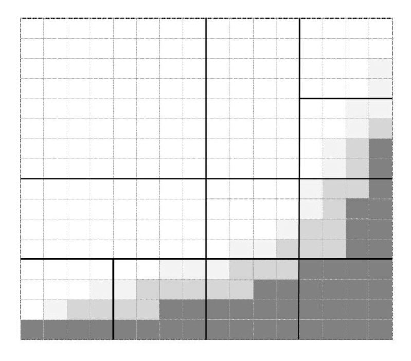
Here v = (vi,vj) is the motion vector relative to the current macro-block. This equation requires 256 subtractions, 256 absolutes and 255 additions and when performed over all the search points in the ±32 search window, requires over two million arithmetic operations per macro-block. Comparison complexity can be reduced by partitioning the 16 × 16 macro-block into 16 groups each with 4 × 4 pixels [22]. Each partition is now represented by a sum of all the pixels in the partition and comparison computation is done using this reduced 16 element vector. The total computation per search point reduces to 71 operations with this approach. In general, the number of computations for each macro-block comparison decreases with reduced number of partitions. For example with a 2 × 2 partition, i.e., with each partition having a size of 8 × 8 pixels, the number of operations reduces to 33. However the overall compression quality could degrade in general. But when the macro-block is from a portion of the image with uniform background, like a wall for instance, then reducing the number of partitions doesn't compromise compression quality. This motivates an adaptive partitioning scheme, where an analysis of the macro-block indicates how fine to partition the macro-block [21]. Hadamard transform coefficients, along with the pixel variances for the macro-block are used to come up with the optimal partition. Figure 10 illustrates an example of a macro-block with an edge in the lower right corners. Since the top left of the macro-block is uniform, a large partition of 8 × 8 suffices in this region. The partitions next to it are of size 8 × 4 and 4 × 4 respectively. Finally the partitions to the right and bottom are all smaller with size 4 × 4 pixels, ensuring that the edge doesn't get smeared out across the partitions.
Table 2 shows the relative savings in the computations and power of the adaptive partitioning scheme [21] when compared to a fixed partitioning scheme of 4 × 4 partitions [22]. The second entry indicates a power increase using this technique, even though the number of computations is reduced. This happens due to power overheads of using additional structures like FIFOs in an actual implementation, which are not captured by just counting the number of computations.

4. Dynamic Power Management System

We have seen the basic tools that are provided by the hardware for dynamic power control. These include knobs to adjust frequency, supply voltage and hardware resources like number of engines and word length. Work load estimation is another key ingredient of a dynamic power management system. In static estimation schemes, the computation loads are determined a priori via profiling [13,16]. Further power improvements are possible if dynamic estimation techniques are used. In a queue based approach, a FIFO is used to queue the tasks that need to be worked on. The FIFO depth then gives an indication of the mismatch between the hardware computation rate and the task arrival rate. The power management control system continuously adjusts the frequency (and hence the voltage) to keep the FIFO depth within some bounds [23,24]. Lee et al. use an artificial neural network to estimate the work load for every image frame in a object recognition application. The neural network uses the work load history of the past frames as well as some preprocessed information of the current frame, to estimate the computing load. The estimated load is then used to set the appropriate voltage and frequency value for the engine [25].
In general we can envision a run-time power management system which continually adapts the power consumption according the work load [26]. The system is modeled to have many power-performance states, where, in each state, the power consumed is related to the performance delivered. For example, in each power domain which is controlled by a power gating transistor, one can identify at least two states: an active state where the domain is connected to the supply and an asleep state where it is disconnected. If clock gating is used, then an intermediate inactive state can be defined where the domain has power, but is idle as clock is stopped. Many different active states are possible, if DVFS is used, each V-F value corresponding to a separate active state. The state transitions of the system incur a time and energy cost and the goal of the run-time power manager is to minimize the power consumption of the system while adapting to the computing load [26].

5. Conclusions

Adaptive power management techniques like Dynamic Power Switching, Dynamic Voltage and Frequency Scaling and Adaptive Voltage Scaling have become common place in many chips. We expect further enhancements and widespread adoption of adaptive techniques in the future due to three fundamental driving forces: Rising chip design costs, increasing process variability, increasing numbers of battery operated appliances. Rising chip costs imply that a single design will attempt to cover a wide range of applications. Hence one can expect a large dynamic range in the computational demands on such chips. Increased process variations in deep sub-micron nodes will imply a large spread in the voltage-frequency relationship for the chips. Finally the rise of battery powered applications forces the designer to extract power efficiencies from all possible design strategies. This naturally leads to adaptive techniques to help chips be power efficient across a large range of computation loads in advanced process nodes with large process variations.
Figure 1. A collection of most commonly used dynamic power management techniques.
Jlpea 01 00261f1
Figure 2. (a) IP block with power switch to support dynamic power switching; (b) SRAM with power switching and standby state retention support.
Jlpea 01 00261f2
Figure 3. A low latency frequency configuration scheme for Dynamic Frequency Scaling.
Jlpea 01 00261f3
Figure 4. Critical Path Monitoring Technique using a reconfigurable delay chain as the replica path and a time digitizer.
Jlpea 01 00261f4
Figure 5. Locus of constant frequency under Dynamic Voltage and Threshold Scaling.
Jlpea 01 00261f5
Figure 6. Savings provided by DVTS beyond that of DVS in a 90 nm process node for a 27 stage ring oscillator with 1% switching activity.
Jlpea 01 00261f6
Figure 7. Dynamic Voltage and Threshold Scaling System.
Jlpea 01 00261f7
Figure 8. In-Situ Difference Power Monitor for a DVTS System.
Jlpea 01 00261f8
Figure 9. Architecture of a power scalable receiver. The receiver's data path can work at a number of different word lengths and sampling frequencies. An adaptivity control unit is added to determine the right word length and sampling frequency which minimizes overall power consumption.
Jlpea 01 00261f9
Figure 10. Partition of a 16 × 16 macro-block into 11 partitions, based on the edge features. The top left 8 × 8 sub-blocks have no further partitions. The edges lie mostly within each partition.
Jlpea 01 00261f10
Table 1. Bit resolution and sampling rate settings for minimum power dissipation for different signal and interference strengths.
Low SNRHigh SNR
High Interference8-bits, 15 MHz, 3.3 mW1-bit, 2 MHz, 0.5 mW
Low Interference2-bits, 15 MHz, 2.49 mW1-bit, 2 MHz, 0.49 mW
Table 2. Comparison of computation and power when using adaptive partitioning instead of fixed 4 × 4 partitions.
Video Sequence, Resolution, Number of FramesComputations ReductionPower Reduction
Viper Train, 1920 × 1080, 31666.15%78.15%
Riverbed, 1920 × 1080, 25093.14%100.67%
Pedestrian, 1920 × 1080, 37573.63%86.45%
Sunflower, 1920 × 1080, 49484.28%95.81%

Acknowledgments

We thank Department of Information Technology, Ministry of Communications and Information Technology, Government of India, for funding support.

References

  1. Staunstrup, J.; Wolf, W. Hardware/Software Co-Design: Principles and Practice; Kluwer Academic Publishers: Norwell, MA, USA, 2010. [Google Scholar]
  2. Rabaey, J. Low Power Design Essentials; Springer: New York, NY, USA, 2009. [Google Scholar]
  3. Benini, L.; de Micheli, G. Dynamic Power Management: Design Techniques and CAD Tools, 1st ed.; Kluwer Academic Publishers: Norwell, MA, USA, 1998. [Google Scholar]
  4. Gammie, G.; Wang, A.; Mair, H.; Lagerquist, R.; Chau, M.; Royannez, P.; Gururajrao, S.; Ko, U. SmartReflex power and performance management technologies for 90 nm, 65 nm, and 45 nm mobile application processors. Proc. IEEE 2010, 98, 144–159. [Google Scholar]
  5. Mutoh, S.; Douseki, T.; Matsuya, Y.; Aoki, T.; Shigematsu, S.; Yamada, J. 1-V power supply high-speed digital circuit technology with multi-threshold voltage CMOS. IEEE J. Solid-State Circuit 1995, 30, 847–854. [Google Scholar]
  6. Flynn, D.; Aitken, R.; Gibbons, A.; Shi, K.J. Low Power Methodology Manual: For System-on-Chip Design; Springer: New York, NY, USA, 2007. [Google Scholar]
  7. Jumel, F.; Royannez, P.; Mair, H.; Scott, D.; Er Rachidi, A.; Lagerquist, R.; Chau, M.; Gururajarao, S.; Thiruvengadam, S.; Clinton, M.; et al. A Leakage Management System Based on Clock Gating Infrastructure for a 65 nm Digital Base-Band Modem Chip. Proceedings of the IEEE Symposium of VLSI Circuits, Honolulu, HI, USA, June 2006; pp. 214–215.
  8. Nakai, M.; Akui, S.; Seno, K.; Meguro, T.; Seki, T.; Kondo, T.; Hashiguchi, A.; Kawahara, H.; Kumano, K.; Shimura, M. Dynamic voltage and frequency management for a low-power embedded microprocessor. IEEE J. Solid-State Circuit 2005, 40, 28–35. [Google Scholar]
  9. Nose, K.; Sakurai, T. Optimization of VDD and VTH for Low-Power and High-Speed Applications. Proceedings of the 2000 Asia and South Pacific Design Automation Conference, ASP-DAC '00, Yokohama, Japan, 25–28 January 2000.
  10. Burd, T.D.; Pering, T.A.; Stratakos, A.G.; Broderson, R.W. A Dynamic voltage scaled microprocessor system. IEEE J. Solid-State Circuit 2000, 35, 1571–1580. [Google Scholar]
  11. Dighe, S.; Vangal, S.R.; Aseron, P.; Kumar, S.; Jacob, T.; Bowman, K.A.; Howard, J.; Tschanz, J.; Erraguntla, V.; Borkar, N.; et al. Within-die variation-aware dynamic-voltage-frequency-scaling with optimal core allocation and thread hopping for the 80-Core TeraFLOPS processor. IEEE J. Solid-State Circuit 2011, 46, 184–193. [Google Scholar]
  12. Bull, D.; Das, S.; Shivashankar, K.; Dasika, G.; Flautner, K.; Blaauw, D. A Power-efficient 32 bit ARM processor using timing-error detection and correction for transient-error tolerance and adaptation to PVT variation. IEEE J. Solid-State Circuit 2011, 46, 18–31. [Google Scholar]
  13. Sreejith, K.; Amrutur, B.; Balivada, A. A workload based lookup table for minimal power operation under supply and body bias control. J. Low Power Electron. 2009, 5, 173–184. [Google Scholar]
  14. Nomura, M.; Ikenaga, Y.; Takeda, K.; Nakazawa, Y.; Aimoto, Y.; Hagihara, Y. delay and power monitoring schemes for minimizing power consumption by means of supply and threshold voltage control in active and standby modes. IEEE J. Solid-State Circuit 2006, 41, 805–814. [Google Scholar]
  15. Mehta, N.; Amrutur, B. Dynamic supply and threshold voltage scaling for CMOS digital circuits using in-situ power monitor. IEEE Trans. Very Large Scale Integr. Syst. 2011, 99, 1–10. [Google Scholar]
  16. Kikuchi, Y.; Takahashi, M.; Maeda, T.; Fukuda, M.; Koshio, Y.; Hara, H.; Arakida, H.; Yamamoto, H.; Hagiwara, Y.; Fujita, T.; et al. A 40 nm 222 mW H.274 full-HD decoding, 25 power domains, 14-core application processor with x512b stacked DRAM. IEEE J. Solid-State Circuit 2011, 46, 32–41. [Google Scholar]
  17. Chandrakasan, A.; Gutnik, V.; Xanthopoulos, T. Data Driven Signal Processing: An Approach for Energy Efficient Computing. Proceedings of the 1996 International Symposium on Low Power Electronics and Design, Monterey, CA, USA, 12–14 August 1996; pp. 347–352.
  18. Sinha, A.; Chandrakasan, A.P. Energy Efficient Filtering Using Adaptive Precision and Variable Voltage. Proceedings of the Twelfth Annual IEEE International ASIC/SOC Conference, IEEE ASIC '99, Washington, DC, USA, 15–18 September 1999; pp. 327–331.
  19. Nisar, M.; Chatterjee, A. Environment and Process Adaptive Low Power Wireless Baseband Signal Processing Using Dual Real-Time Feedback. Proceedings of the 22nd International Conference on VLSI Design, New Delhi, India, 5–9 January 2009.
  20. Dwivedi, S.; Amrutur, B.; Bhat, N. Power Scalable Digital Baseband Architecture for IEEE 802.15.4. Proceedings of the 24th International Conference on VLSI Design, Chennai, India, 2–7 January 2011.
  21. Gupte, A.; Amrutur, B. Adaptive global elimination algorithm for low power motion estimation. J. Low Power Electron. 2009, 5, 1–16. [Google Scholar]
  22. Huang, Y.-W.; Chien, S.-Y.; Hsieh, B.-Y.; Chen, L.-G. Global elimination algorithm and architecture for fast block matching motion estimation. IEEE Trans. Circuit Syst. Video Technol. 2004, 14, 898–907. [Google Scholar]
  23. Gutnik, V.; Chandrakasan, A. An Energy Efficient Controller for Variable Supply Voltage Low Power Processing. Proceedings of the 1996 International Symposium on Circuits and Systems, Atlanta, GA, USA, 12–15 May 1996; pp. 158–159.
  24. Lu, Z.; Hein, J.; Humphrey, M.; Stan, M.; Lach, J.; Skadron, K. Control-Theoretic Dynamic Frequency and Voltage Scaling for Multimedia Workloads. Proceedings of the 5th International Conference on Compilers, Architecture, and Synthesis for Embedded Systems, CASES '02, Greenoble, France, 8–11 October 2002.
  25. Lee, S.; Oh, J.; Park, J.; Kwon, K.; Kim, M.; Yoo, H.-J. A 345 mW heterogeneous many-core processor with an intelligent inference engine for robust object recognition. Proceedings of the 2010 IEEE International Solid-State Circuits Conference, San Francisco, CA, USA, 7–11 February 2010; pp. 332–333.
  26. Simunic, T.; Benini, L.; Glynn, P.; de Micheli, G. Dynamic Power Management for Portable Systems. Proceedings of the 6th Annual International Conference on Mobile Computing and Networking (MobiCom '00), Boston, MA, USA, 6–11 August 2000.