A Low Impact Ionization Rate Poly-Si TFT with a Current and Electric Field Split Design

 ,
, 
Abstract
:1. Introduction
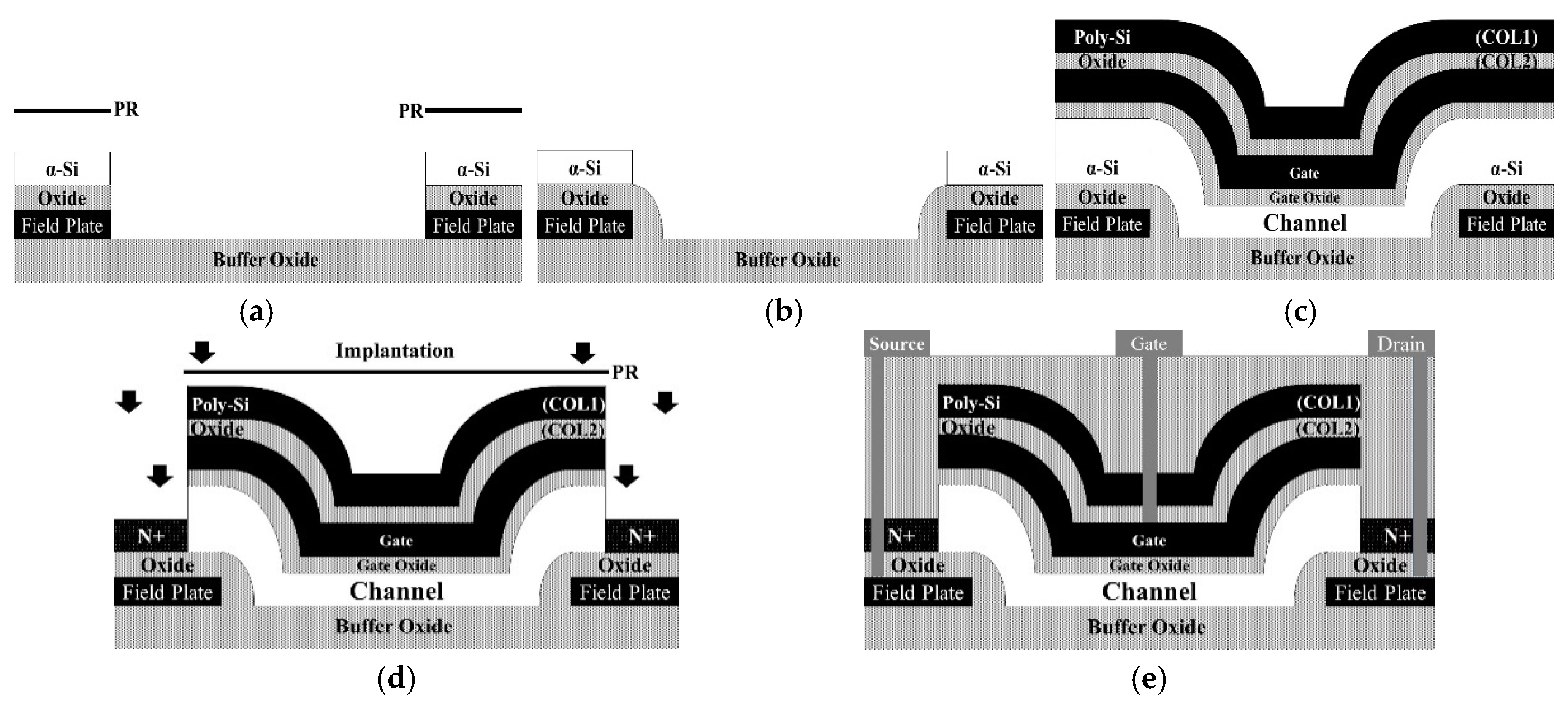
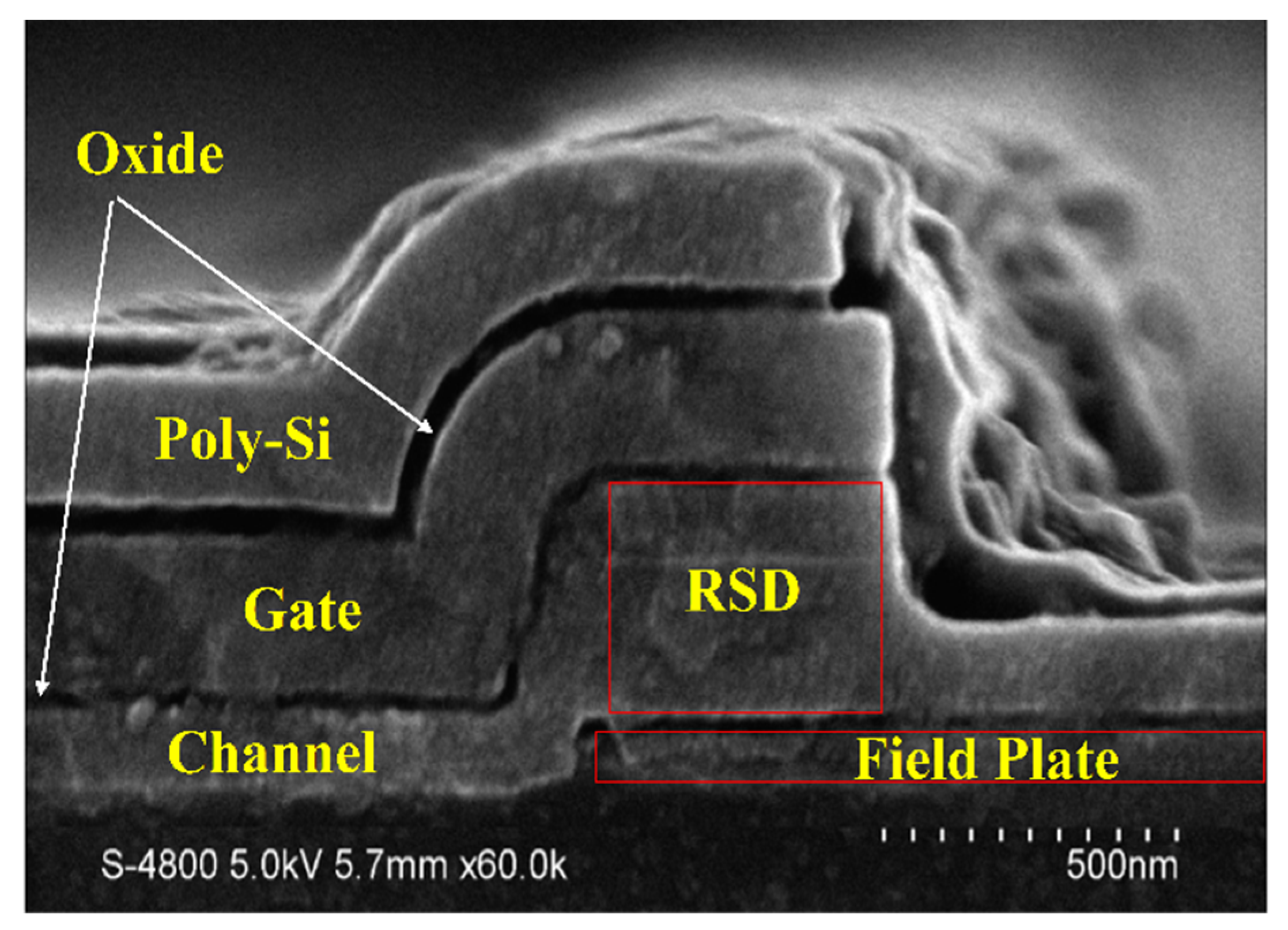
2. Device Fabrication
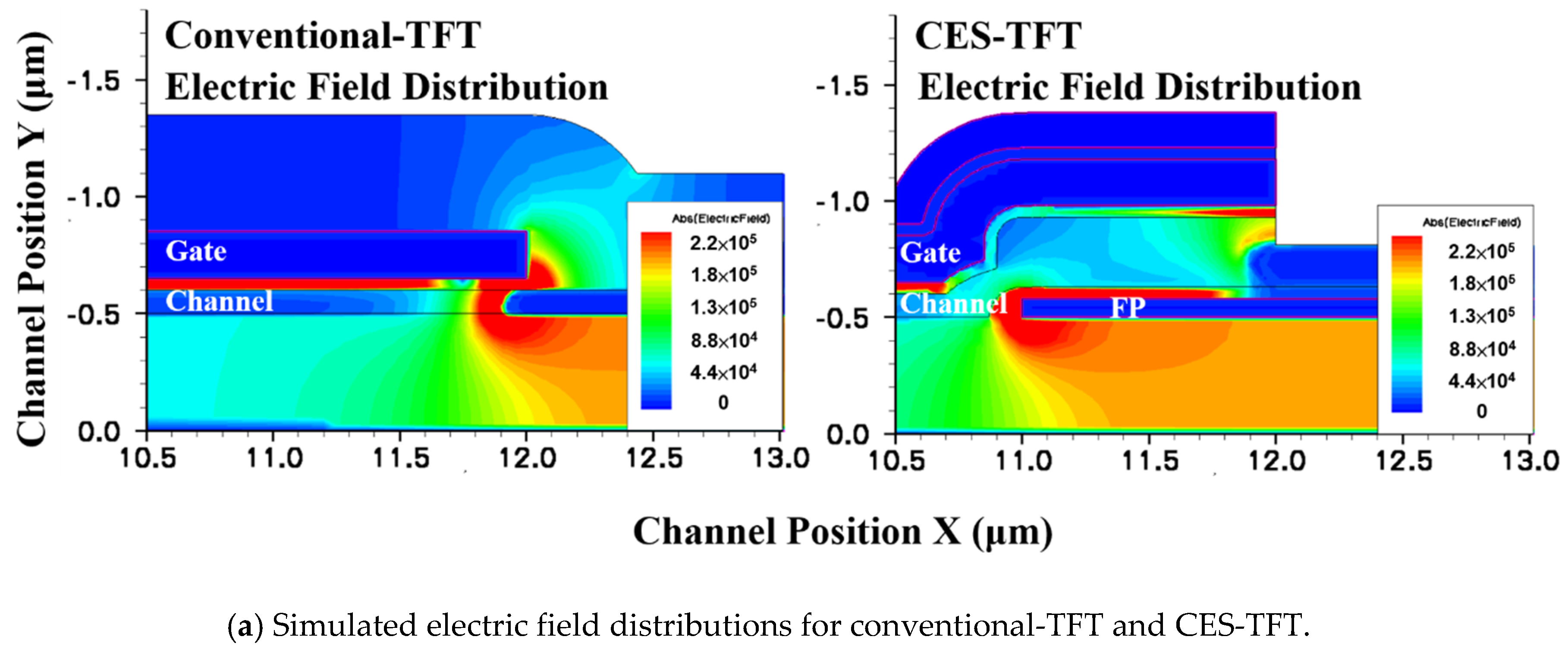
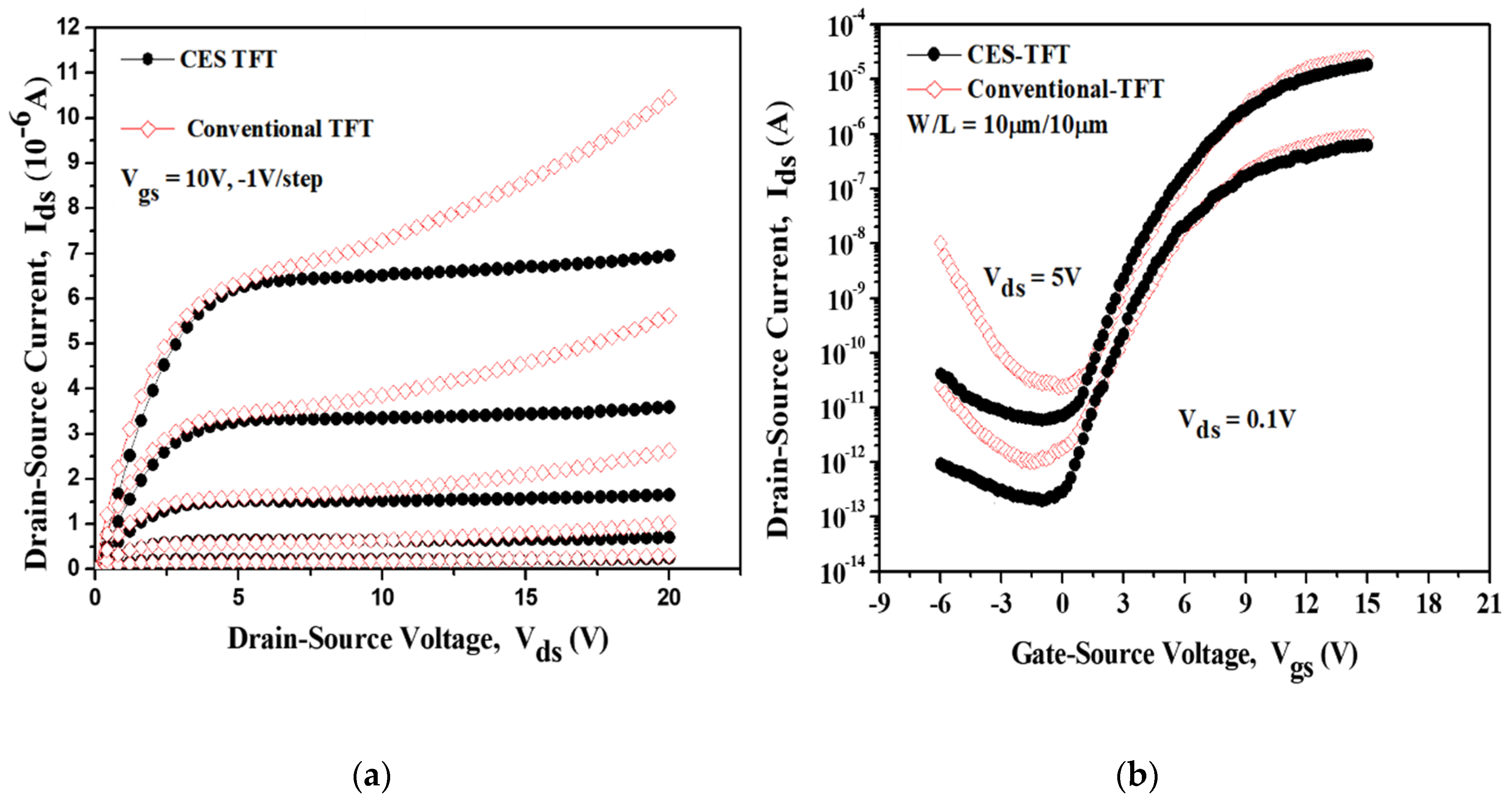
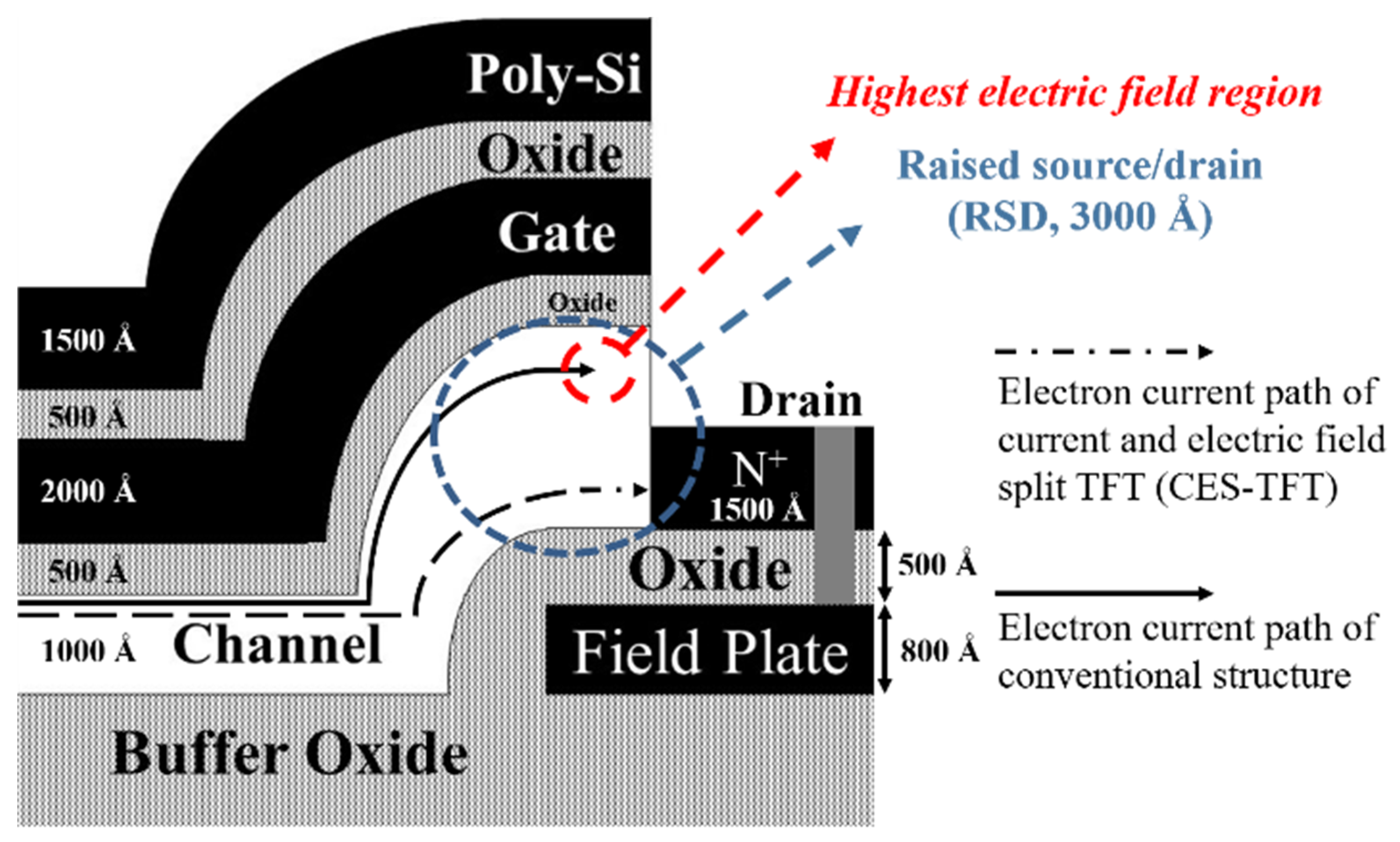
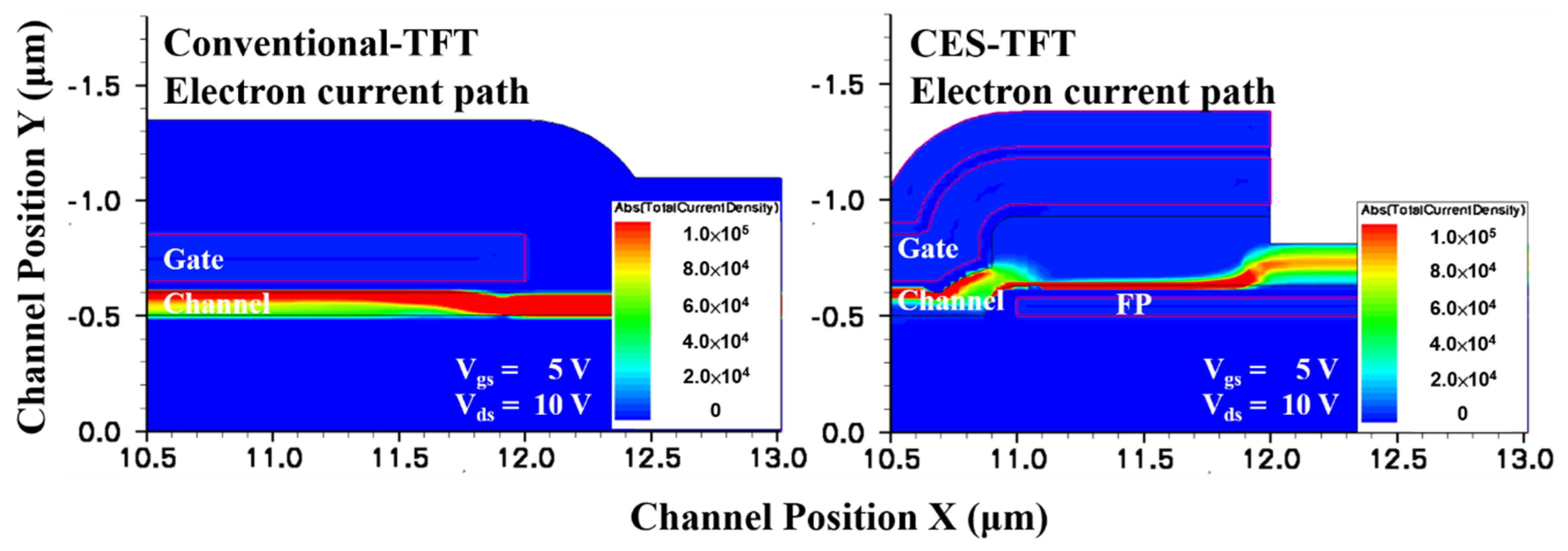
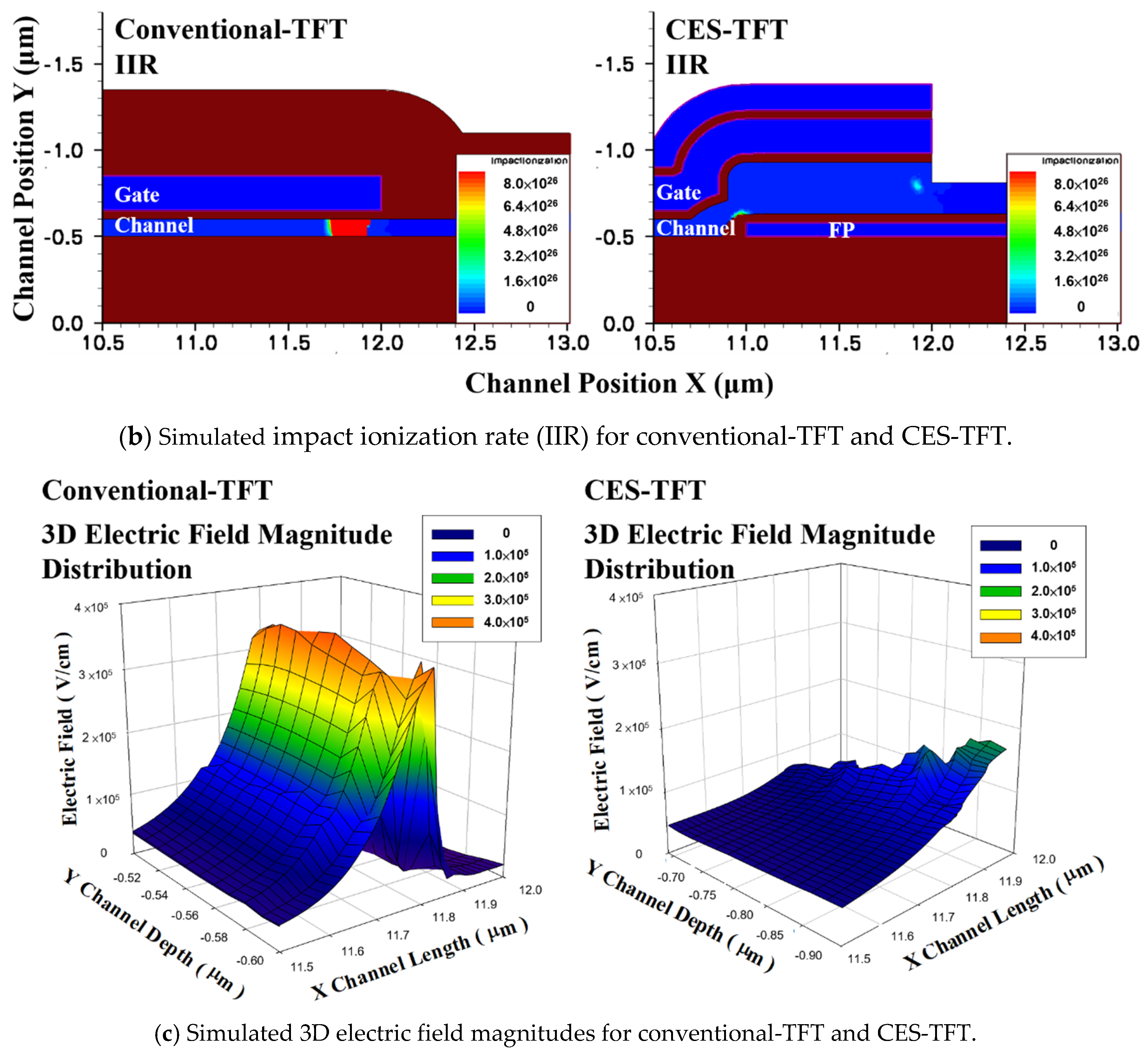
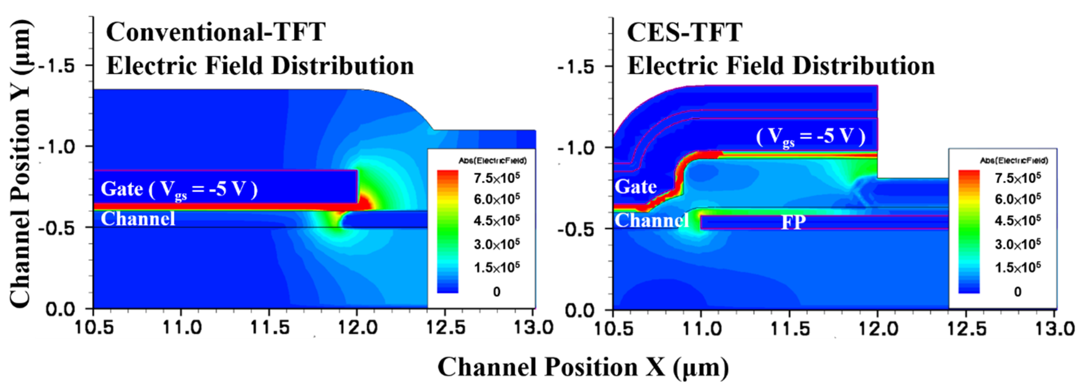
3. Structure Simulation, Device Measurement, and Discussion
4. Conclusions
Author Contributions
Funding
Conflicts of Interest
References
- Liu, T.C.; Kuo, J.B.; Zhang, S. Floating-body kink-effect-related parasitic bipolar transistor behavior in poly-si tft. IEEE Electron Device Lett. 2012, 33, 842–844. [Google Scholar] [CrossRef]
- Ho, C.-H.; Lu, C.; Roy, K. An enhanced voltage programming pixel circuit for compensating gb-induced variations in poly-si tfts for amoled displays. J. Disp. Technol. 2014, 10, 345–351. [Google Scholar] [CrossRef]
- Olasupo, K.; Hatalis, M. Leakage current mechanism in sub-micron polysilicon thin-film transistors. IEEE Trans. Electron Devices 1996, 43, 1218–1223. [Google Scholar] [CrossRef]
- KP, A.K.; Sin, J.K.; Nguyen, C.T.; Ko, P.K. Kink-free polycrystalline silicon double-gate elevated-channel thin-film transistors. IEEE Trans. Electron Devices 1998, 45, 2514–2520. [Google Scholar]
- Mariucci, L.; Fortunato, G.; Bonfiglietti, A.; Cuscuna, M.; Pecora, A.; Valletta, A. Polysilicon tft structures for kink-effect suppression. IEEE Trans. Electron Devices 2004, 51, 1135–1142. [Google Scholar] [CrossRef]
- Li, X.; Geng, D.; Mativenga, M.; Jang, J. High-speed dual-gate a-igzo tft-based circuits with top-gate offset structure. IEEE Electron Device Lett. 2014, 35, 461–463. [Google Scholar] [CrossRef]
- Lee, U.G.; Mativenga, M.; Kang, D.H.; Jang, J. A three-mask-processed coplanar a-igzo tft with source and drain offsets. IEEE Electron Device Lett. 2012, 33, 812–814. [Google Scholar] [CrossRef]
- Zhan, S.; Han, R.; Chan, M.J. A novel self-aligned bottom gate poly-si tft with in-situ ldd. IEEE Electron Device Lett. 2001, 22, 393–395. [Google Scholar] [CrossRef]
- Kimura, M. Behavior analysis of an ldd poly-si tft using 2-d device simulation. IEEE Trans. Electron Devices 2012, 59, 705–709. [Google Scholar] [CrossRef]
- Park, J.-h.; Kim, O. A novel self-aligned poly-si tft with field-induced drain formed by the damascene process. IEEE Electron Device Lett. 2005, 26, 249–251. [Google Scholar] [CrossRef]
- Ahn, J.-A.; Kim, O. Influence of field-induced drain on the characteristics of poly-si thin-film transistor using a self-aligned double spacer process. Jpn. J. Appl. Phys. 2004, 43, 897. [Google Scholar] [CrossRef]
- Chang, K.M.; Lin, G.M.; Yang, G.L. A novel low-temperature polysilicon thin-film transistors with a self-aligned gate and raised source/drain formed by the damascene process. IEEE Electron Device Lett. 2007, 28, 806–808. [Google Scholar] [CrossRef]
- Chien, F.-T.; Chen, C.-W.; Lee, T.-C.; Wang, C.-L.; Cheng, C.-H.; Kang, T.-K.; Chiu, H.-C. A novel self-aligned double-channel polysilicon thin-film transistor. IEEE Trans. Electron Devices 2012, 60, 799–804. [Google Scholar] [CrossRef]
- Chien, F.-T.; Chen, Y.-J. A kink-effect-free poly-si thin-film transistor with current and electric field split structure design. IEEE Trans. Electron Devices 2010, 57, 2547–2555. [Google Scholar] [CrossRef]
- Chien, F.-T.; Yu, C.-H.; Chen, C.-W.; Cheng, C.-H.; Kang, T.-K.; Chiu, H.-C. A high-current kink effect free z-gate poly–si thin-film transistor. IEEE Electron Device Lett. 2016, 37, 886–889. [Google Scholar] [CrossRef]
- ISE-TCAD Manuals, release 10.0; Integrated Systems Engineering: Zurich, Switzerland, 2004.
- Valdinoci, M.; Colalongo, L.; Baccarani, G.; Pecora, A.; Policicchio, I.; Fortunato, G.; Plais, F.; Legagneux, P.; Reita, C.; Pribat, D. Analysis of electrical characteristics of polycrystalline silicon thin-film transistors under static and dynamic conditions. Solid-State Electron. 1997, 41, 1363–1369. [Google Scholar] [CrossRef]
- Armstrong, G.; Brotherton, S.; Ayres, J. A comparison of the kink effect in polysilicon thin film transistors and silicon on insulator transistors. Solid-State Electron. 1996, 39, 1337–1346. [Google Scholar] [CrossRef]


© 2019 by the authors. Licensee MDPI, Basel, Switzerland. This article is an open access article distributed under the terms and conditions of the Creative Commons Attribution (CC BY) license (http://creativecommons.org/licenses/by/4.0/).
Share and Cite
Chien, F.-T.; Hsueh, K.-P.; Hong, Z.-J.; Lin, K.-T.; Tsai, Y.-T.; Chiu, H.-C. A Low Impact Ionization Rate Poly-Si TFT with a Current and Electric Field Split Design. Coatings 2019, 9, 514. https://doi.org/10.3390/coatings9080514
Chien F-T, Hsueh K-P, Hong Z-J, Lin K-T, Tsai Y-T, Chiu H-C. A Low Impact Ionization Rate Poly-Si TFT with a Current and Electric Field Split Design. Coatings. 2019; 9(8):514. https://doi.org/10.3390/coatings9080514
Chicago/Turabian StyleChien, Feng-Tso, Kuang-Po Hsueh, Zhen-Jie Hong, Kuan-Ting Lin, Yao-Tsung Tsai, and Hsien-Chin Chiu. 2019. "A Low Impact Ionization Rate Poly-Si TFT with a Current and Electric Field Split Design" Coatings 9, no. 8: 514. https://doi.org/10.3390/coatings9080514
APA StyleChien, F.-T., Hsueh, K.-P., Hong, Z.-J., Lin, K.-T., Tsai, Y.-T., & Chiu, H.-C. (2019). A Low Impact Ionization Rate Poly-Si TFT with a Current and Electric Field Split Design. Coatings, 9(8), 514. https://doi.org/10.3390/coatings9080514