Article

Nickel Film Deposition with Varying RF Power for the Reduction of Contact Resistance in NiSi

1
Department of Electronics Engineering, Chungnam National University, Daejeon 34134, Korea
2
School of Integrated Technology, Yonsei Institute of Convergence Technology, Yonsei University, Incheon 21983, Korea
*
Author to whom correspondence should be addressed.
Coatings 2019, 9(6), 349; https://doi.org/10.3390/coatings9060349
Submission received: 10 May 2019 / Revised: 23 May 2019 / Accepted: 27 May 2019 / Published: 28 May 2019
(This article belongs to the Special Issue Advanced Strategies in Thin Film Engineering by Magnetron Sputtering)

Abstract

:
In this study, the effect of radio frequency (RF) power on nickel (Ni) film deposition was studied to investigate the applications of lowering the contact resistance in the NiSi/Si junction. The RF powers of 100, 150, and 200 W were used for the deposition of the Ni film on an n/p silicon substrate. RMS roughnesses of 1.354, 1.174 and 1.338 nm were obtained at 100, 150, and 200 W, respectively. A circular transmission line model (CTLM) pattern was used to obtain the contact resistance for three different RF-power-deposited films. The lowest contact resistivity of 5.84 × 10⁻⁵ Ω-cm2 was obtained for the NiSi/n-Si substrate for Ni film deposited at 150 W RF power.

1. Introduction

Nickel silicide (NiSi) is a promising metal silicide material for the fabricating source/drain (S/D) contacts in electronic devices; the downscaling of a device leads to an uncontrollable increase in the contact resistance in the S/D and gate electrodes [1,2,3]. NiSi, by virtue of its characteristic properties such as its low-temperature processing, low silicon consumption, and low resistivity phase compared to other metal silicides, has been studied intensively by various research groups. Ramly et al. reported a study on the controlled diffusion of Ni in the formation of NiSi with different Ni thicknesses for the application of a supercapacitor electrode [4]. Vijselaar et al. studied the effect of a NiSi interlayer on Si substrates for the fabrication of a photoelectrode for photocatalytic properties [5]. Marshall et al. reported the NiSi as a passivated tunneling contact for application in high-efficiency solar cells [6]. However, obtaining a low-resistivity NiSi phase still remains a critical issue for high-efficiency electronic devices. In this context, obtaining low-resistance NiSi is essential for high-performance devices. Previous reports have shown that, by controlling the Ni diffusion through Si, the NiSi phase can be selectively obtained. Kousseifi et al. used a Pt intermixed layer to control the NiSi phase [7]. Jung et al. used an ultraviolet laser to obtain NiSi through a photo-thermal process [8]. Fouet et al. studied the silicide formation using different Ni film thicknesses to control NiSi formation [9]. Tous et al. obtained the direct formation of the NiSi phase using the excimer laser annealing (ELA) process [10]. Different methods have been reported for growing NiSi films for various applications. Kwang et al. studied the interfacial properties of NiSi films deposited by using atomic layer deposition [11]. Mahdi et al. reported well-aligned NiSi/SiC core-shell nanowire growth by hot-wire chemical vapor deposition to enhance the electrical properties of NiSi [12]. Koichi et al. introduced a cyclic deposition process using molecular beam epitaxy (MBE) to grow NiSi for low-resistance films [13]. Azimirad et al. studied the thermal stability of NiSi film by a co-sputtering process and reported the thermal stability of NiSi to be improved by using a platinum interlayer structure on the Si substrate [14].
Therefore, greater understanding of the formation and control of NiSi is needed. To achieve this, the quality and stability of the Ni film are also very important. Ni films can be deposited by various methods such as chemical vapor deposition (CVD), atomic layer deposition (ALD), sputtering, MBE, thermal evaporation, pulsed laser deposition, electroplating [15,16,17,18,19,20,21], etc. Among these techniques, vapor deposition through conventional sputtering still remains the most widely used process for metal film deposition. However, to date, the effect of RF power on the contact resistance of the NiSi/Si junctions has not been reported.
In this study, Ni films were deposited with different RF powers, and the influence of the RF power on its surface and structural properties was investigated. Finally, NiSi was obtained by the rapid temperature annealing (RTA) of the different Ni films, and the contact resistance was measured using the circular transmission line model (CTLM) procedure.

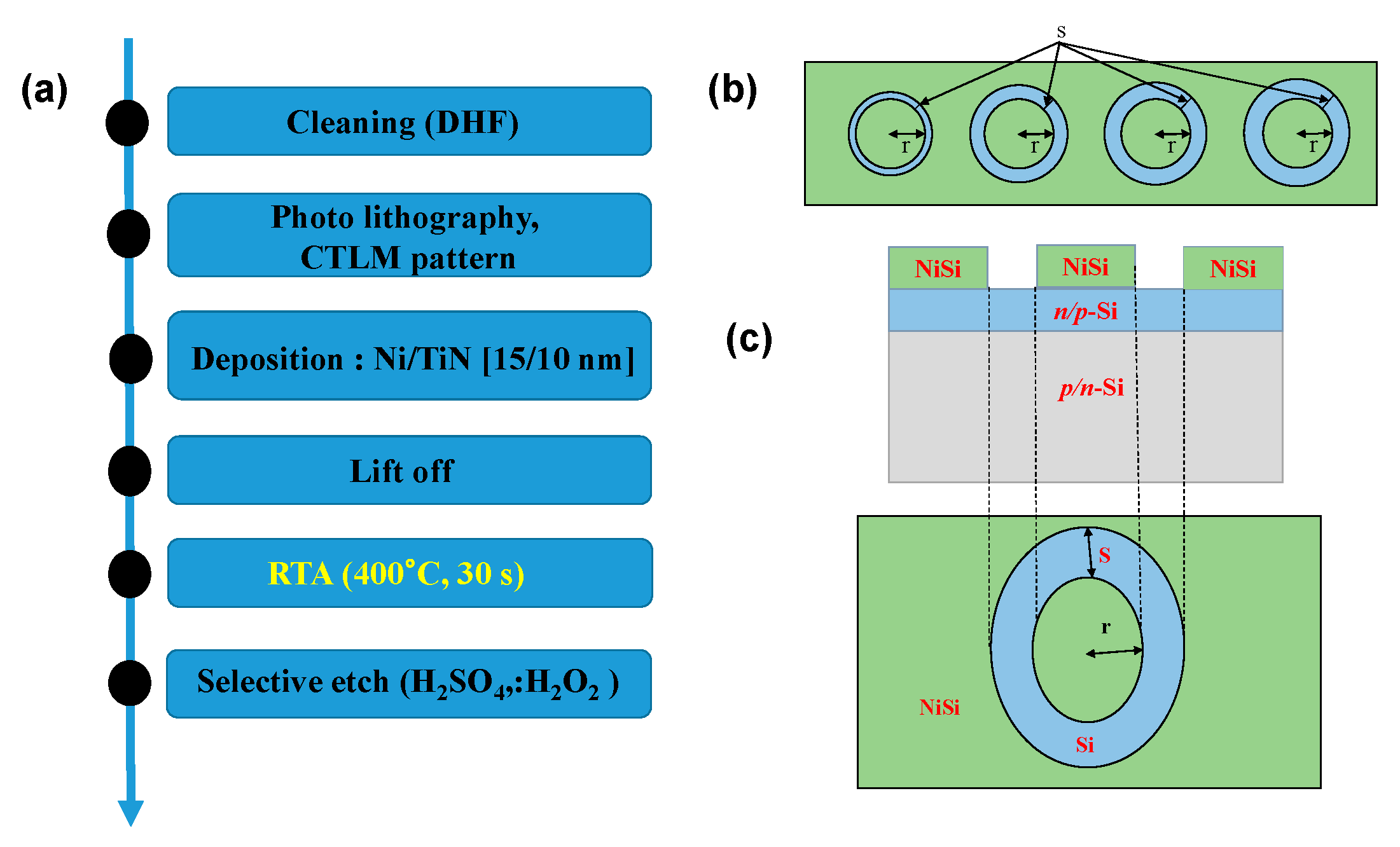
2. Materials and Methods

2.1. Ni Films Deposition

The Ni film samples were deposited by using an RF sputtering process on Si (100) substrates. Initially, the substrates were cleaned in dilute HF solution for 150 s and subsequently rinsed in de-ionized water and dried using nitrogen purging. Then, the samples were inserted into the sputtering chamber until the base pressure of the sputtering chamber reached 5.0 × 10⁻⁷ Torr. After that, an argon flow of 1.8 sccm flowed into the chamber, and the chamber pressure was maintained at 2.5 mTorr using a pressure gauge. The Ni film was deposited at three different RF powers of 100, 150, and 200 W and the deposition time was fixed to 20 min.

2.2. Nickel Silicide Fabrication and Contact Resistance Measurement

Two types of Si substrates were used to measure the contact resistance of NiSi. Arsenic (As) and boron fluoride (BF2) were used as n and p dopants, by ion implantation with a dose of 5 × 1015 cm−2 at 50 keV to obtain n/p-Si substrates, respectively. The in-situ deposition of nickel followed by titanium nitride Ni/TiN [15/10 nm] was performed on n/p-Si substrates at optimized conditions of an Ar flow rate 1.8 sccm and a chamber pressure of 2.5 mTorr and different RF powers of 100, 150 and 200 W, followed by the RTA process at 400 °C for 30 s to obtain NiSi. The TiN film was used as a capping layer to prevent the oxidation of Ni during thermal annealing. The CTLM pattern was fabricated on the substrates to measure the contact resistance. Figure 1 shows the experimental flow chart.
The structural and surface morphologies were characterized using an X-ray diffractometer (XRD, D/MAX 2500PC, Rigaku, Japan) with CuKα radiation, atomic force microscopy (AFM, MAF20 VEECO, New York, NY, USA), and field-emission scanning electron microscopy (FESEM, Hitachi, S-4800, Tokyo, Japan). The contact resistance was measured using a Kelvin four-point probe (Alessi REL-6100 Cascade Microtech, Beaverton, OR, USA).

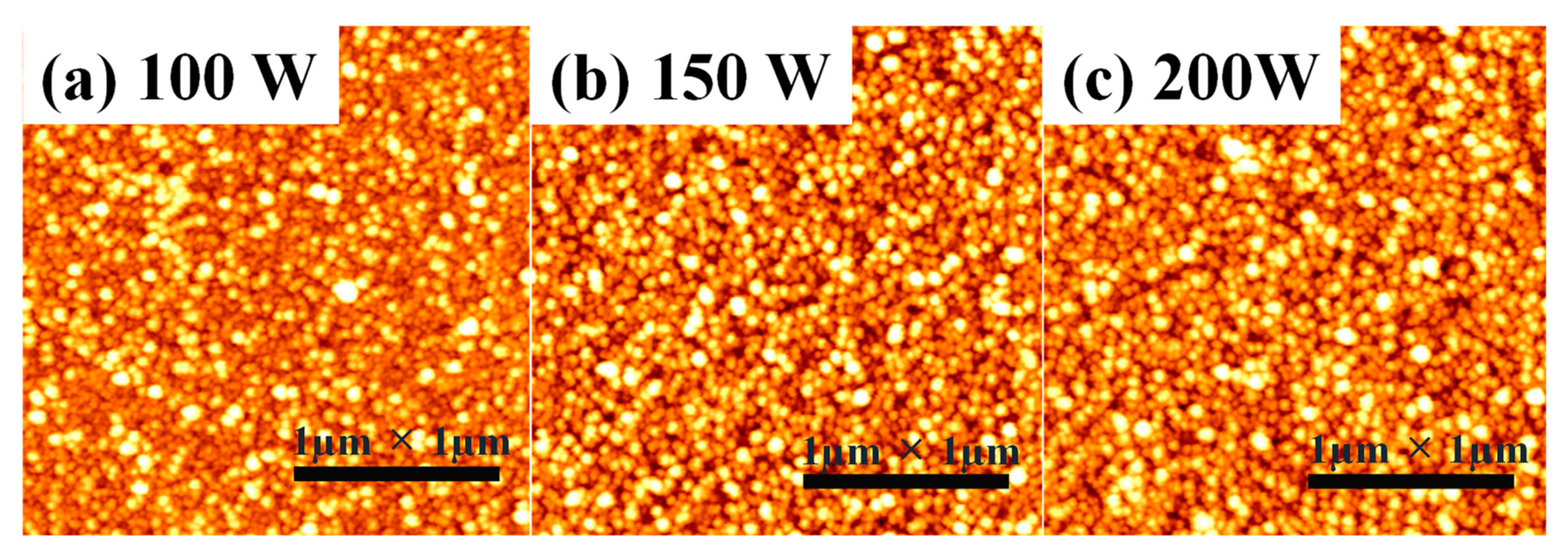
3. Results and Discussion

The influence of the RF sputtering power was investigated, keeping all other parameters, such as gas pressure and Ar flow, fixed at 2.5 mTorr and 1.8 sccm, respectively. Figure 2 shows the plot of thickness and resistivity as a function of the sputtering power. The plot result shows that by increasing the RF power, the rate of film deposition increases while the resistivity of the film gradually decreases. The average lowest and highest thicknesses of the deposited Ni films obtained were 61.3 and 100 nm at 100 and 200 W, respectively. The decrease in the resistivity with an increase in the RF power could be due to the decrease in the Ni film crystallite size and surface uniformity. The lowest resistivity of 1.69 × 10⁻⁵ Ω-cm was obtained for the 150 W-deposited film. It is possible that as the RF power increased, more Ar ions accelerated to hit the Ni target under high power, resulting in more Ni particles being ejected from the target with increased kinetic energy and velocity, resulting in a faster deposition rate. The high sputtering power improved the crystallization of the Ni films and aided in the formation of the Ni films with highly dense microstructures, which, as a result, led to a reduction in the resistivity [22,23].
To check the surface morphology of the Ni films deposited at various RF powers, FESEM images were taken and are shown in Figure 3. The cross-sectional and surface morphology of the Ni film deposited at 100 W is shown in Figure 3a-1,a-2. The average film thickness of the Ni film was 61.3 nm and the surface shows uniform grain disturbance. However, we notice small cracks on the surface of the Ni film. Further, with an increase in the RF power, the Ni film thickness increased. The average thicknesses of the Ni films were 81.7 and 100 nm for RF powers of 150 and 200 W, respectively, as shown in Figure 3b-2,c-2. The surface morphology of the films shows a bigger crystallite size compared to the 100 W Ni film.
The structural properties of the films deposited at various magnitudes of RF power are shown in Figure 4. The main peaks at 44.75°, 54.88°, 76.41° are indexed to Ni (111), Ni (200) and Ni (220), which are attributed to Ni’s face-centered cubic (FCC) structure [24]. This indicates that the Ni films were in a well-defined crystalline state during deposition. The average crystallite size of the film was determined from the FWHM of the (111) diffraction peaks using Scherrer’s equation [25],
D p = K λ β cos θ
where Dp is the average crystallite size, Κ = Scherrer constant (0.94), λ is the x-ray wavelength (λ = 1.54178 Å), β is the full width half maximum (FWHM) of the (111) peak, and θ is the Bragg angle. It was found that the crystallite size varied between 13.59, 16.24, and 14.91 nm as the RF power changed from 100–200 W. According to the calculations, the crystallite size gradually increased with an increase in the RF power until 150 W, which offered the highest crystallite size, and then gradually decreased. It could be that, with an increase in RF power higher than 150 W, the crystalline quality of film decreases, as evident from the decrease in the relative Ni (111) peak intensity at the higher RF power of 200 W.
To analyze the surface roughness of the Ni films deposited at different RF powers, AFM measurements were obtained. Figure 5 shows the AFM images at different RF powers. The RMS values of the Ni films obtained were 1.354, 1.174, and 1.338 nm. It was noted that the Ni film surface roughness decreases at 150 W and gradually increases at 200 W, indicating that the Ni films deposited at higher RF powers show lower film quality. It is observed that the RF power has an influence on the surface structure of Ni films. The Ni films grown at 150 W RF power have a comparatively low kinetic energy of sputtered particles compared to 200 W RF power, which leads to a relatively more random orientation and various sizes of grain growth, which lead to a rough surface.
To investigate the effect of RF power on the contact resistance, NiSi films were formed with three different RF powers: 100, 150, and 200 W. An Ni film of 15 nm was deposited using different sputtering powers on the Si substrates. Prior to deposition, the deposition rates were calculated for all three RF powers, and the corresponding sheet resistances were measured. The deposition rates were calculated by depositing Ni for different growth times of 11–14 min, and plots of thickness versus growth time and deposition rate were obtained by a linear fit. The deposition rates were found to be 4.6, 5.1, and 7.1 nm/min at 100, 150, and 200 W, respectively.
In the next section, the three RF conditions are referred to as RF-1, RF-2, and RF-3. Initially, to investigate the lowest sheet resistance of the NiSi phase, Ni films deposited on Si substrates were annealed to form NiSi. The RTA process was performed on the samples with varying temperatures from 300–700 °C for 30 s in a N2 atmosphere. Figure 6 shows the plot of sheet resistance (Rsh) verse RTA temperature; it can be observed that Rsh decreases with increasing temperature from 300 °C until 450 °C, and with further increase in temperature, the Rsh increases drastically. It is well known that at a lower temperature (300–400 °C), the NiSi phase predominantly exists, and with an increase in the temperature, Rsh increases. The lowest Rsh values of 6.04 and 6.46 Ω/sq. were obtained for RF-2 on p and n-Si substrates, respectively. Above the RTA temperature of 550 °C, the sheet resistance increases drastically due to the predominant formation of NiSi2, which is the high-resistance phase. Zhao et al. have reported that above 500 °C, the agglomeration of NiSi increases and irregular nucleation of NiSi2 starts, which leads to an increase in resistance [26].
The specific contact resistance ρC between the Si substrate and NiSi for the three different Ni films were extracted using a 4-wire Kelvin resistance measurement, and ρC was determined using the following equations [27]:
R T = R sh 2 π r ( s + 2 L T ) C
C = r s ln ( 1 + s r )
ρ C = R sh L T 2
where Rsh is the sheet resistance, C is the correction factor, LT is the effective transfer length, r is the radius of the inner circle, which was fixed at 80 mm, and s is the gap space, which was split as 8, 12, 16, 20, 24, 32, 40, and 48 mm. Rsh and LT can be determined via a linear fit of RT at the different gap space values. Figure 7 shows the plot of total resistance measured as a function of the gap space between the inner and outer rings of the NiSi layers for RF-1, RF-2, and RF-3. The lower total contact resistivities of 5.84 × 10⁻⁵ Ω-cm2 for n-Si and 6.58 × 10⁻⁵ Ω-cm2 for p-Si are obtained for the RF-2 film, respectively, and the reduction in contact resistance is lower than the Ni Ohmic contacts previously reported [28]. Thus, by controlling the film deposition using RF power, the quality of the NiSi formation can be controlled. A similar conclusion was reported by Gordillo et al. in their work done on the effect of RF power on electrical properties of Mo films. They concluded from their study that a decrease in the resistivity of Mo films was caused by changing the RF power [29]. In our case, different RF powers control the grain size and surface roughness of the Ni films and show different NiSi electrical characteristics.
Table 1 shows the measured values of the contact resistivity and transfer length of the NiSi on n/p-Si substrates. Thus, from the results, it could be that Ni films deposited with an RF power of 150 W showed lower contact resistance in comparison to the Ni films at 100 and 200 W power. It is well known that Ni film and Si substrate undergo a sequential reaction from Ni2Si to NiSi and finally to NiSi2 with an increase in the RTA temperature [30,31,32]. In our case, the formation of the sequence of Ni silicide phases of the three films varied with the Ni deposition rate and RTA temperature. The Ni film deposited at 150 W could have controlled the NiSi phase with lower resistivity compared to the other two RF powers. These results lead to the conclusion that, by controlling the Ni film deposition rates, it is possible to obtain low-resistivity NiSi for future electronic devices.

4. Conclusions

In this study, Ni films formed at three different RF powers of 100, 150, and 200 W were investigated for low-resistivity NiSi contacts. The result analysis shows a decrease in the resistivity of Ni films with an increase in RF power. The XRD and AFM data on the Ni films clearly support the change in the resistivity with RF power change. Further, low contact resistance NiSi films were formed by annealing the Ni films, and their contact resistances were measured. The total resistance of 5.84 × 10⁻⁵ Ω-cm2 was obtained for 150 W RF power. The results clearly show that the NiSi formed at 150 W showed lower resistance than NiSi formed at 100 and 200 W. This study is meaningful in that a thin Ni film with a low resistivity was formed by varying the RF power in sputtering, and the formed NiSi phase showed a low contact resistance.

Author Contributions

Conceptualization and Supervision, H.-D.L.; Methodology and Writing—Original Draft Preparation, S.B.E., H.-S.S.; Writing—Review and Editing, H.-D.S., H.-D.L. and J.W.O.; Funding Acquisition, H.-D.L.

Funding

This research was funded by the MOTIE (Ministry of Trade, Industry & Energy (10048536) and the KSRC (Korea Semiconductor Research Consortium) support program for the development of future semiconductor devices. This research was also supported by the Ministry of Trade, Industry and Energy (MOTIE) (10067808) and the Korea Semiconductor Research Consortium (KSRC) support program for the development of future semiconductor devices.

Conflicts of Interest

The authors declare no conflict of interest.

References

  1. Rabab, R.B.; Amir, N.H.; Arwa, T.K.; Abdurrahman, G.; Muhammad, M.H. Impact of nickel silicide rear metallization on the series resistance of crystalline silicon solar cells. Energy Technol. 2018, 6, 1627–1632. [Google Scholar]
  2. Geenen, F.A.; Van Stiphout, K.; Nanakoudis, A.; Bals, S.; Vantomme, A.; Jordan-Sweet, J.; Lavoie, C.; Detavernier, C. Controlling the formation and stability of ultra-thin nickel silicides—An alloying strategy for preventing agglomeration. J. Appl. Phys. 2018, 123, 075303. [Google Scholar] [CrossRef]
  3. Wolansky, D.; Grabolla, T.; Lenke, T.; Schulze, S.; Zaumseil, P. Impact of nickel silicide on SiGe BiCMOS devices. Semicond. Sci. Technol. 2018, 33, 124003. [Google Scholar] [CrossRef]
  4. Ramly, M.M.; Omar, F.S.; Rohaizad, A.; Aspanut, Z.; Rahman, S.A.; Goh, B.T. Solid-phase diffusion controlled growth of nickel silicide nanowires for supercapacitor electrode. Appl. Surf. Sci. 2018, 456, 515–525. [Google Scholar] [CrossRef]
  5. Vijselaar, W.; Tiggelaar, R.M.; Gardeniers, H.J.; Huskens, J. Efficient and stable silicon microwire photocathodes with a nickel silicide interlayer for operation in strongly alkaline solutions. ACS Energy Lett. 2018, 3, 1086–1092. [Google Scholar] [CrossRef] [PubMed]
  6. Marshall, A.; Florent, K.; Tapriya, A.; Lee, B.G.; Kurinec, S.K.; Young, D.L. Nickel silicide metallization for passivated tunneling contacts for silicon solar cells. In Proceedings of the IEEE 43rd Photovoltaic Specialists Conference (PVSC), Portland, OR, USA, 5–10 June 2016; pp. 2479–2482. [Google Scholar]
  7. El Kousseifi, M.; Hoummada, K.; Bertoglio, M.; Mangelinck, D. Selection of the first Ni silicide phase by controlling the Pt incorporation in the intermixed layer. Acta Mater. 2016, 106, 193–198. [Google Scholar] [CrossRef]
  8. Jung, S.M.; Kim, J.H.; Park, C.J.; Shin, M.W. Nickel mono-silicide formation using a photo-thermal process assisted by ultra-violet laser. Mater. Sci. Semicond. Process. 2018, 75, 263–268. [Google Scholar] [CrossRef]
  9. Richard, M.-I.; Mangelinck, D.; Guichet, C.; Thomas, O.; Texier, M.; Fouet, J.; Boudet, N.; Portavoce, A. Silicide formation during reaction between Ni ultra-thin films and Si (001) substrates. Mater. Lett. 2013, 116, 139–142. [Google Scholar]
  10. Tous, L.; Lerat, J.-F.; Emeraud, T.; Negru, R.; Huet, K.; Uruena, A.; Aleman, M.; Russell, R.; John, J.; Poortmans, J.; et al. Nickel silicide formation using excimer laser annealing. Energy Procedia 2012, 27, 503–509. [Google Scholar] [CrossRef]
  11. Lee, K.M.; Kim, C.Y.; Choi, C.K.; Yun, S.W.; Ha, J.B.; Lee, J.H.; Lee, J.Y. Interface properties of nickel-silicide films deposited by using plasma-assisted atomic layer deposition. J. Korean Phys. Soc. 2009, 55, 1153–1157. [Google Scholar] [CrossRef]
  12. Alizadeh, M.; Hamzan, N.B.; Ooi, P.C.; Bin Omar, M.F.; Dee, C.F.; Goh, B.T. Solid-state limited nucleation of NiSi/SiC core-shell nanowires by hot-wire chemical vapor deposition. Materials 2019, 12, 674. [Google Scholar] [CrossRef]
  13. Terashima, K.; Miura, Y.; Ikarashi, N.; Oshida, M.; Manabe, K.; Yoshihara, T.; Tanaka, M.; Wakabayashi, H. Formation of Nickel Self-Aligned Silicide by Using Cyclic Deposition Method. In Proceedings of the 2004 International Conference on Solid State Devices and Materials, Tokyo, Japan, 14–17 September 2004; pp. 182–183. [Google Scholar]
  14. Azimirad, R.; Kargarian, M.; Akhavan, O.; Moshfegh, A.Z. Improved thermal stability of NiSi nanolayer in Ni-Si Co-sputtered structure. Int. J. Nanosci. Nanotechnol. 2011, 7, 14–20. [Google Scholar]
  15. Guo, Q.; Guo, Z.; Shi, J.; Sang, L.; Gao, B.; Chen, Q.; Liu, Z.; Wang, X. Fabrication of nickel and nickel carbide thin films by pulsed chemical vapor deposition. MRS Commun. 2018, 8, 88–94. [Google Scholar] [CrossRef]
  16. Han, W.S.; Kim, S.; Hwang, J.; Park, J.-M.; Koh, W.; Lee, W.-J. Plasma-enhanced atomic layer deposition of nickel thin film using is (1,4-diisopropyl-1,4-diazabutadiene) nickel. J. Vac. Sci. Technol. A Vacuum Surf. Film 2017, 36, 01A119. [Google Scholar]
  17. Widodo, S. Characterization of Thin Film Nickel (Ni) Deposition by Sputtering Method. Int. J. Innov. Sci. Technol. 2015, 2, 380–385. [Google Scholar]
  18. Nishiyama, T.; Tanaka, T.; Shikada, K.; Ohtake, M.; Kirino, F.; Futamoto, M. Growth of Ni Thin Films on Al2O3 Single-Crystal Substrates. Jpn. J. Appl. Phys. 2009, 48, 13003. [Google Scholar] [CrossRef]
  19. Valladares, L.D.L.S.; Ionescu, A.; Holmes, S.; Barnes, C.H.W.; Dominguez, A.B.; Quispe, O.A.; Gonzalez, J.C.; Milana, S.; Barbone, M.; Ferrari, A.C.; et al. Characterization of Ni thin films following thermal oxidation in air. J. Vac. Sci. Technol. B 2014, 32, 51808. [Google Scholar] [CrossRef]
  20. Kassem, W.; Roumie, M.; Tabbal, M. Pulsed Laser Deposition of Tungsten Thin Films on Graphite. Adv. Mater. 2011, 324, 77–80. [Google Scholar] [CrossRef]
  21. Li, J.-D.; Zhang, P.; Wu, Y.-H.; Liu, Y.-S.; Xuan, M. Uniformity study of nickel thin-film microstructure deposited by electroplating. Microsyst. Technol. 2009, 15, 505–510. [Google Scholar] [CrossRef]
  22. Peri, B.; Borah, B.; Dash, R.K. Effect of RF power and gas flow ratio on the growth and morphology of the PECVD SiC thin film s for MEMS applications. Mater. Sci. 2015, 38, 1105–1112. [Google Scholar] [CrossRef] [Green Version]
  23. Posadowski, W.; Wiatrowski, A.; Kapka, G. Effect of pulsed magnetron sputtering process for the deposition of thin layers of nickel and nickel oxide. Mater. Sci. 2018, 36, 69–74. [Google Scholar] [CrossRef]
  24. Vergara, J.; Madurga, V. Structure and magnetic properties of Ni films obtained by pulsed laser ablation deposition. J. Mater. 2002, 17, 2099–2104. [Google Scholar] [CrossRef]
  25. D’Agostino, A.T. Determination of thin metal film thickness by X-ray diffractometry using the Scherrer equation, atomic absorption analysis and transmission/reflection visible spectroscopy. Anal. Chim. Acta 1992, 262, 269–275. [Google Scholar] [CrossRef]
  26. Zhao, F.F.; Zheng, J.Z.; Shen, Z.X.; Osipowicz, T.; Gao, W.Z.; Chan, L.H. Thermal stability study of NiSi and NiSi2 thin films. Microelectron. Eng. 2004, 71, 104–111. [Google Scholar] [CrossRef]
  27. Schroder, D.K. Semiconductor Material and Device Characterization, 3rd ed.; John Wiley & Sons, Inc.: Hoboken, NJ, USA, 2006; p. 144. ISBN 9780471739067. [Google Scholar]
  28. Kuchuk, A.V.; Borowicz, P.; Wzorek, M.; Borysiewicz, M.; Ratajczak, R.; Golaszewska, K.; Kaminska, E.; Kladko, V.; Piotrowska, A. Ni-based ohmic contacts to n-type 4H-SiC: The formation mechanism and thermal stability. Adv. Condens. Matter Phys. 2016, 2016, 26. [Google Scholar] [CrossRef]
  29. Gordillo, G.; Mesa, F.; Calderón, C. Electrical and morphological properties of low resistivity Mo thin Films prepared by magnetron sputtering. Braz. J. Phys. 2006, 36, 982–985. [Google Scholar] [CrossRef]
  30. Zhang, S.-L.; Smith, U. Self-aligned silicides for Ohmic contacts in complementary metal–oxide–semiconductor technology: TiSi2, CoSi2, and NiSi. J. Vac. Sci. Technol. A Vacuum Surf. Film 2004, 22, 1361–1370. [Google Scholar] [CrossRef]
  31. Chen, X.; Zhang, B.; Li, C.; Shao, Z.; Su, D.; Williams, C.T.; Liang, C. Structural and electrochemical properties of nanostructured nickel silicides by reduction and silicification of high-surface-area nickel oxide. Mater. Res. Bull. 2012, 47, 867–877. [Google Scholar] [CrossRef]
  32. Lauwers, A.; Kitt, J.A.; Van Dal, M.J.H.; Chamirian, O.; Pawlak, M.A.; De Potter, M.; Lindsay, R.; Raymakers, T.; Pages, X.; Mebarki, B. Ni based suicides for 45 nm CMOS and beyond. Mater. Sci. Eng. B Solid-State Mater. Adv. Technol. 2004, 114–115, 29–41. [Google Scholar] [CrossRef]
Figure 1. (a) Fabrication flow chart of nickel silicide (NiSi) formations and (b,c) circular transmission line model (CTLM) pattern. r is the radius of the inner circle, and s the radius difference between the inner and outer circle (gap space) and the schematic diagram of NiSi on the Si substrate.
Coatings 09 00349 g001
Figure 2. The plot of the Ni films’ average thickness and resistivity versus RF power.
Coatings 09 00349 g002
Figure 3. FESEM surface and cross-sectional images of Ni films deposited at different RF powers: 100 W (a-1,a-2), 150 W (b-1,b-2) and 200 W (c-1,c-2). The same scale is used for all images (500 nm).
Coatings 09 00349 g003
Figure 4. X-Ray diffraction plots of Ni films deposited at different RF powers.
Coatings 09 00349 g004
Figure 5. The AFM images Ni films deposited at various RF powers: (a) 100 W, (b) 150 W and (c) 200 W.
Coatings 09 00349 g005
Figure 6. The plot of sheet resistance verses RTA temperature plot of NiSi on n/p-Si formed with different RF powers.
Coatings 09 00349 g006
Figure 7. The plot of the total resistance versus gap space of the CTLM pattern for the extraction of specific contact resistivity’s with different RF powers.
Coatings 09 00349 g007
Table 1. The values of the contact resistivity and transfer length of the NiSi on n/p-Si substrates.
Sample NiSi/n-SiNiSi/p-Si
RF PowerρC [Ω-cm2]LT [μm]ρC [Ω-cm2]LT [μm]
Ni/TiN
[15/10 nm]
100 W8.08 × 10−58.1287.82 × 10−54.663
150 W5.84 × 10−57.4936.58 × 10−54.787
200 W1.18 × 10−4 10.296.94 × 10−54.411

