Article

Observation of the Magnetization Reorientation in Self-Assembled Metallic Fe-Silicide Nanowires at Room Temperature by Spin-Polarized Scanning Tunneling Spectromicroscopy

1
Department of Electrophysics, National Chiayi University, Chiayi 60004, Taiwan
2
Institute of Optoelectronics and Solid State Electronics, National Chiayi University, Chiayi 60004, Taiwan
*
Author to whom correspondence should be addressed.
Coatings 2019, 9(5), 314; https://doi.org/10.3390/coatings9050314
Submission received: 4 March 2019 / Revised: 5 May 2019 / Accepted: 8 May 2019 / Published: 10 May 2019
(This article belongs to the Special Issue Metal-Semiconductor and Insulator-Semiconductor Interfaces)

Abstract

:
The quasi-periodic magnetic domains in metallic Fe-silicide nanowires self-assembled on the Si(110)-16 × 2 surface have been observed at room temperature by direct imaging of both the topographic and magnetic structures using spin-polarized scanning tunneling microscopy/spectroscopy. The spin-polarized differential conductance (dI/dV) map of the rectangular-sectional Fe-silicide nanowire with a width and height larger than 36 and 4 nm, respectively, clearly shows an array of almost parallel streak domains that alternate an enhanced (reduced) density of states over in-plane (out-of-plane) magnetized domains with a magnetic period of 5.0 ± 1.0 nm. This heterostructure of magnetic Fe-silicide nanowires epitaxially integrated with the Si(110)-16 × 2 surface will have a significant impact on the development of Si-based spintronic nanodevices.

1. Introduction

Recent investigations have shown that the heterostructures of magnetic transition-metal silicides grown epitaxially on silicon substrates are potential candidates for spin injection into silicon, not only because magnetic transition-metal silicides possess a large electron-spin polarization, but also because they form an atomically smooth interface with silicon to achieve highly efficient spin injection [1,2,3]. Moreover, silicon substrates have been regarded as ideal hosts for spin transport because of their long spin relaxation time, which leads to a long spin diffusion length in spintronic devices [4,5]. Since transition-metal silicides are widely used as Ohmic or Schottky barrier contacts and as low-resistance interconnections in conventional microelectronics, one of the most important goals of “spintronics” is to combine silicon technology with magnetic transition-metal silicides to develop silicon-based spintronic nanodevices to realize spin injection into silicon [6,7]. In particular, it is highly desirable to fabricate high-quality heterostructures of magnetic transition-metal silicide nanowires (NWs) grown epitaxially on silicon surfaces because the spins act coherently within magnetic NWs to modulate electron transport in a single direction, producing unusual ferromagnetic properties [8,9,10,11,12,13,14].
The self-assembly of epitaxial silicide NWs on silicon surfaces has been the subject of intensive study because the spontaneous formation of spatially ordered silicide NWs over a large area provides a promising route for fabricating the building blocks of nanodevices without the need for masking and patterning [15,16,17,18]. The Si(110)-16 × 2 surface is known to act as a one-dimensional nanotemplate for the self-formation of massively parallel-aligned silicide NWs with a single orientation [15,16,17]. Moreover, the complementary metal–oxide–semiconductor field-effect transistor (CMOSFET) on Si(110) could be a promising alternative because the p-type CMOSFET switch is about 30% faster in the (110) substrate compared with the (100) substrate, and CMOSFET on Si(110) exhibits a higher hole mobility than those on Si(100) [19]. Thus, the self-assembly of large-area magnetic silicide NWs on Si(110) surfaces opens up the possibility for future wafer-scale integration of high-density Si-based spintronic nanodevices in a bottom-up scheme.
Spin-polarized scanning tunneling microscopy/spectroscopy (SP-STM/STS) is a powerful tool for imaging magnetic domains of magnetic nanostructures with subnanometer resolution, which allows for the detailed investigation of the interplay between the structural, electronic, and magnetic properties of magnetic NWs [20,21]. In this article, we report the direct imaging of the magnetic structures of self-assembled metallic Fe-silicide NWs on the Si(110)-16 × 2 surface using SP-STM/STS measurements at room temperature (RT). A multidomain magnetic configuration of almost parallel streak domains, repeating with a periodicity of 5.0 ± 1.0 nm, was clearly observed in rectangular-sectional Fe-silicide NWs with a width and height larger than 36 and 4 nm, respectively. This multidomain configuration exhibits a quasi-periodic magnetization modulation with alternating in-plane and out-of-plane domains, based on the explanation of the noncollinear magnetism in a bulk Ni tip. Our results unambiguously show that self-assembled metallic Fe-silicide NWs on the Si(110)-16 × 2 surface are ferromagnetically ordered at RT. This heterojunction of magnetic Fe-silicide NWs epitaxially integrated with Si(110)-16 × 2 surface will have a significant impact on the development of Si-based spintronic nanodevices working at RT.

2. Experiments

The experiments were performed in a commercial ultrahigh-vacuum STM system with a base pressure of ~5 × 10⁻¹¹ mbar. N-type Si(110) samples (10 Ω cm) were used as nanotemplates for the self-assembly of parallel-aligned Fe-silicide NWs. Atomically clean Si(110)-16 × 2 surfaces were prepared by well-established annealing procedures [22,23], and were confirmed by the STM observations (see Figure 1) of Si(110)-16 × 2 reconstructions. Fe-silicide NWs were produced by depositing ~30 nm of high-purity (99.995%) Fe onto the Si(110)-16 × 2 surface at 600 °C, followed by annealing at 700 °C for 20 min. The Fe coverage was determined in situ using a quartz crystal thickness monitor. SP-STM/STS measurements were acquired in the current imaging tunneling spectroscopy (CITS) mode [24] at RT with an electrochemically etched nickel (Ni) tip to detect the differential conductance (dI/dV) of spin-polarized tunneling currents. In CITS mode, maps of the dI/dV (magnetic signal) were recorded simultaneously with constant current images (topography). The different magnetizations of various Fe-silicide NWs can be distinguished from different spin-sensitive dI/dV intensities. Each IV curve was obtained by recording the tunneling current (It) while ramping the bias voltage (Vb) from −2.0 to 2.0 V with a voltage step of 0.05 V. The IV curve was then numerically differentiated to derive a dI/dV curve (i.e., a STS spectrum).

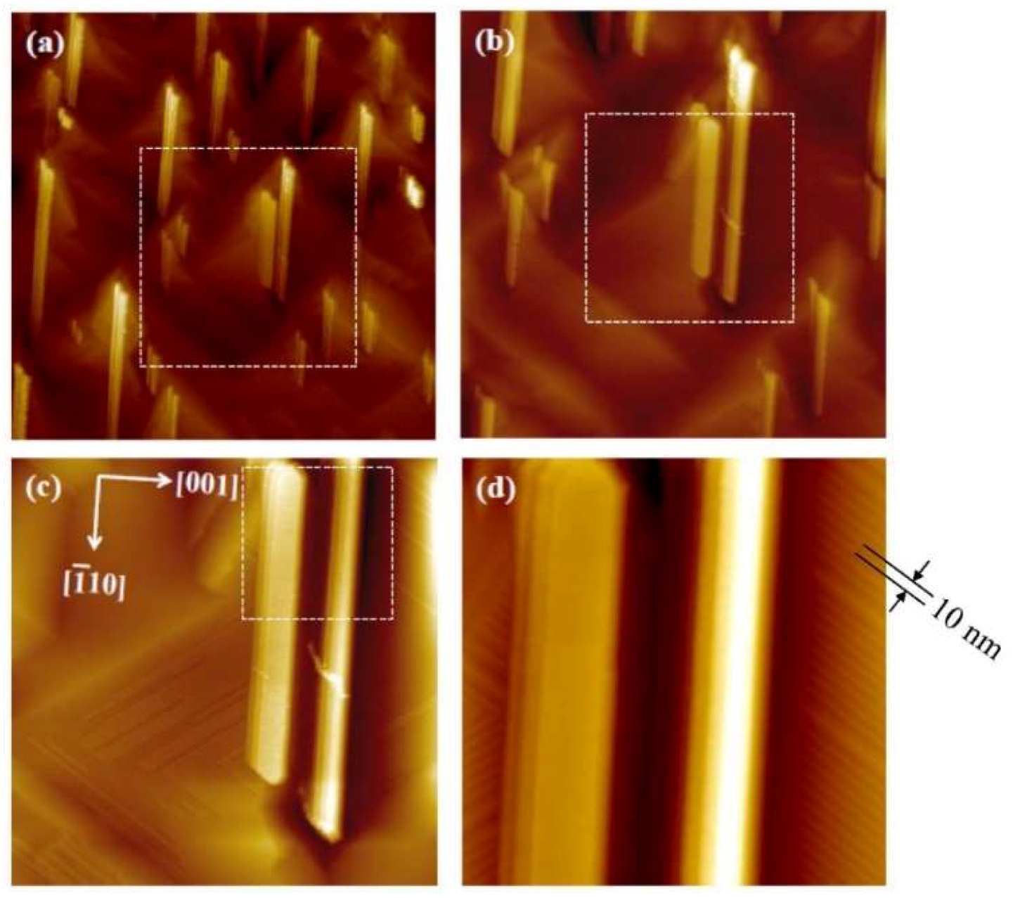
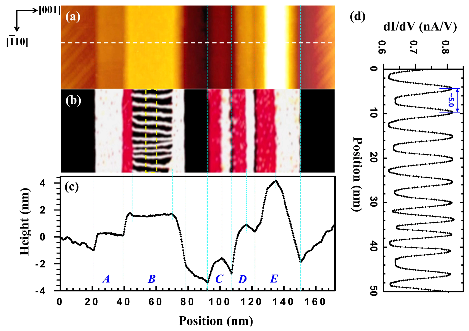
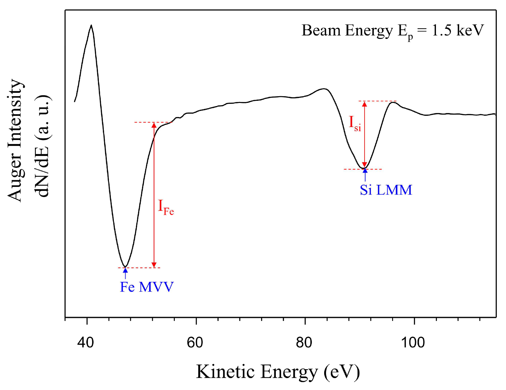
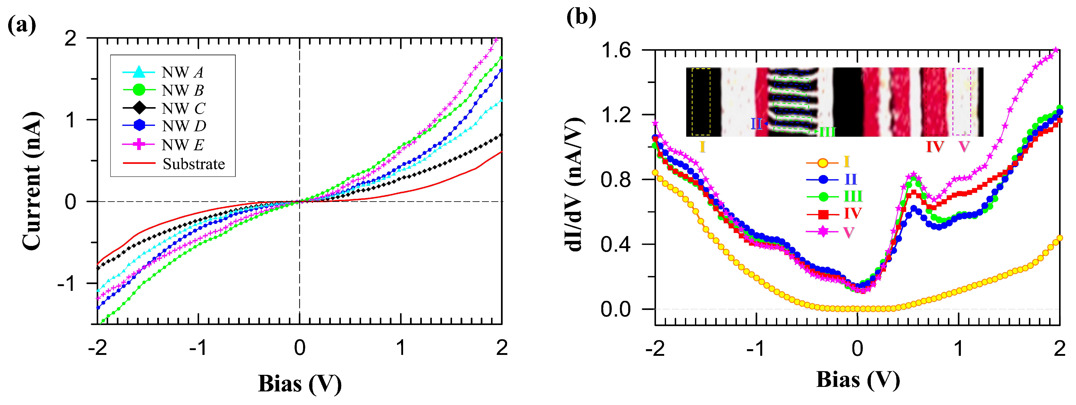
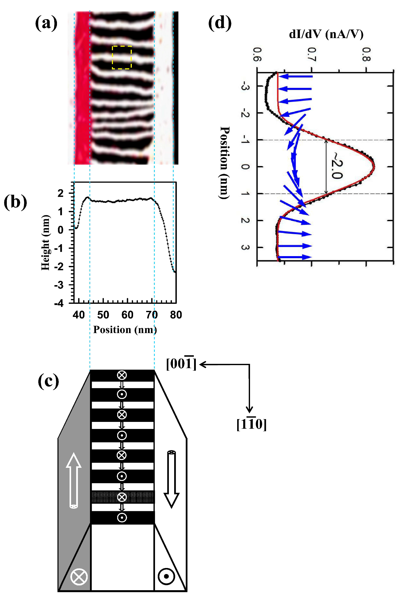
3. Results and Discussion

Figure 2 shows SP-STM topographic images of Fe-silicide NW arrays at different magnifications. As shown in Figure 2a–c, the parallel-aligned and straight NWs covered a macroscopic area with a typical lateral separation of up to 5 μm. It is clear that the self-assembled NWs are highly parallel and elongated along the [ 1 ¯ 10] direction. These NWs are 12–40 nm wide, 1–5 nm high, and 400–700 nm long, respectively. Additionally, as can be seen in Figure 2, these parallel NWs are surrounded by two domains of a long-range grating-like Fe-induced superstructure with a 10 nm periodicity and have adjacent trenches due to local Si depletion. The change in the periodicity (from 5 to 10 nm) of the grating-like superstructures on the Si(110)-16 × 2 surface and the Fe-induced reconstructed surface suggests strong interactions between the Fe and Si atoms. The formation of trenches indicates that Fe-silicide NWs grow into the Si(110) substrate via an “endotaxial” growth mechanism [15,16,25], as manifestly shown in the cross-sectional profile of Figure 3c which could produce a sharp and well-defined interface between NWs and the Si achieving a highly efficient spin injection [15,16]. We also found that these parallel silicide NWs exhibit a multiple-layer NW growth, which was typically observed in previous studies [17,18].
Figure 3a,b show SP-STM images of parallel Fe-silicide NWs on an area different from that of Figure 2d and the corresponding SP-STS image (i.e., SP-dI/dV map). This SP-dI/dV map was acquired at 250 × 125 pixel2. As clearly revealed in Figure 3a,c, there are five parallel-aligned NWs with different morphologies, labeled A to E. Their widths, thicknesses, and lengths are listed in Table 1. The contrast change of the SP-dI/dV map in Figure 3b coincides with the cross-sectional profile of these NWs in Figure 3c. Because no contrast was detected in the dI/dV maps of these parallel Fe-silicide NWs with a tungsten tip, the signal variation in the dI/dV map in Figure 3b thus results from spin-polarized tunneling between the magnetic Ni tip and the magnetic Fe-silicide NWs, not the electronic origin. The observed contrast of the SP-dI/dV map with a Ni tip clearly shows that these parallel Fe-silicide NWs are magnetic at RT. The RT magnetism of Fe-silicide NWs has been reported in previous studies on the magnetic properties of Fe3Si [10,11], Fe5Si3 [12,13], and β-FeSi2 [14] NWs. We have used Auger electron spectroscopy (AES) analysis by measuring the peak height ratio of the Fe MVV (47 eV) and Si LVV (92 eV) lines to determine the stoichiometric ratio (i.e., IFe/ISi) of the parallel Fe-silicide NWs, as shown in Figure 4. AES spectrum shows that the stoichiometric ratio of IFe/ISi in these parallel Fe-silicide NWs is about 1.8, which indicates that these Fe-silicide NWs are likely to be iron-rich phases such as Fe5Si3. This result can be further supported by the metallic character of these parallel NWs shown in the corresponding IV curves (see Figure 5), which is consistent with that of Fe5Si3 NWs and rules out the possibility of semiconducting β-FeSi2 NWs.
To gain insight into the local electronic structure of the five parallel-aligned Fe-silicide NWs (A to E), IV curves were measured on top of the individual NWs and the adjacent substrates, as displayed in Figure 5a. Each representative IV curve is spatially averaged over 20 individual spectra measured along the corresponding NW. All NWs exhibit a metallic character, whereas the adjacent substrate shows semiconducting behavior with a band gap of ~0.9 eV, which is smaller than 1.4 eV obtained for the clean Si(110) surface. The reduced gap of the substrate indicates that the Si(110)-16 × 2 surface reacted with Fe, as shown in Figure 2d (i.e., the periodicity of the grating-like superstructures on the Fe-induced reconstructed substrate changed to 10 nm). Such a ferromagnetic Schottky junction with the Si channel can be used to realize a spin-field-effect transistor. Furthermore, ferromagnetic NWs with good conductivity are ideal for studying one-dimensional electron spin dynamics [26].
Because dI/dV curves allow us to compare the local density of states (LDOS) in the selected areas on the surface, the averaged dI/dV curves of different magnetic domains in NW B are presented in Figure 5b, which are dominated by one pronounced peak at +0.50 V, i.e., the Fe 3d state [27]. The significant difference in the intensity of this 3d peak taken from various magnetic domains is caused by the spin-dependent tunneling magnetoresistance in the magnetic tunnel junctions of SP-STM [20,21], and does not result from spin–orbit induced local electronic structure variations [28]. This spin-dependent state at +0.50 V is the origin of the magnetic contrast in the SP-dI/dV map in Figure 3b.
In Figure 3c, we find that the cross-sectional shape of NWs A and B are rectangular, while NWs C, D, and E show the triangular sections. The SP-dI/dV map in Figure 3b clearly shows the magnetic contrast of the rectangular-sectional NW B with a quasiperiodic pattern of almost parallel streak domains appearing alternately as white and black, where a white or black color indicates high or low dI/dV intensity, respectively. White and black streaks are observed that correspond to different magnetic domain walls. These parallel streak domains are roughly oriented along the [001] direction, perpendicular to the NW. This magnetization modulation is only observed in rectangular-sectional NWs with widths and heights larger than 36 and 4 nm, respectively. As shown in the SP-dI/dV profile in Figure 3d, these repeatedly arranged streak domains alternate with a magnetic period of 5.0 ± 1.0 nm; the white and black streak domains have widths of 2.0 ± 1.0 nm and 3.0 ± 1.0 nm, respectively. As reported in previous studies of domain structures [29,30,31,32], the magnetic domain configuration depends on island thickness, size, and shape. In laterally confined elongated islands and thin films, the shape anisotropy becomes increasingly important, whereas in thick films the magnetocrystalline anisotropy plays an increasing role with decreasing contribution of the shape anisotropy. Thus, the magnetization modulation in the wide and thick NW B originates from the competition between the magnetocrystalline anisotropy along the easy axis and the shape anisotropy along the wire axis. Because the cross-sectional shape of NW E is a sharp triangle, the shape anisotropy is stronger than the magnetocrystalline anisotropy in the laterally confined NW E, which tends to align the magnetization along the NW, as seen in the in-plane magnetization of NW E in Figure 6. Additionally, NWs A, C, and D are laterally confined, with widths of <20 nm (see Table 1); they thus exhibit in-plane magnetization along the wire axis due to the strong shape anisotropy, as shown in Figure 3c.
In Figure 3c, the white contrast of the whole NW A reveals that there is only one single domain in this NW. On the contrary, the magnetic contrast of the left-half region of the three triangular-sectional NWs (i.e., C, D, and E) is different from that of the right-half region, which clearly indicates that the two distinct domains (with the white and red contrasts) exhibit opposite in-plane magnetizations oriented along the individual triangular-sectional NW, as is usually observed in the domain structures of Fe ribbons with inclined surfaces [31,32]. According to References [31,32], the magnetization directions of elongated island domains with inclined surfaces typically exhibit an in-plane orientation. The strong decrease of the dI/dV signal at the edges between the three triangular-sectional NWs is caused by the imperfect performance of the STM feedback. The magnetization direction of the single triangular-sectional NW (i.e., NW E) is schematically represented in Figure 6c, which is compared with the SP-dI/dV map and the cross-sectional profile of NW E in Figure 6a,b. Because the tunneling current depends on the relative orientation between the magnetizations of the measured region and Ni tip, if the magnetization of the measured region is parallel to the tip magnetization, the SP-dI/dV map is bright, while an anti-parallel magnetization results in a darker SP-dI/dV map. Therefore, the white domain in the right-half region of the triangular-sectional NW implies that the magnetizations of this region and the Ni tip are parallel. The magnetization of the red domain in the left-half region is thus antiparallel to that of the Ni tip. Therefore, the Ni tip is also horizontally magnetized along the [ 1 ¯ 10] direction. Such an in-plane sensitivity of the magnetic bulk tip has been reported in a previous SP-STS image with a bulk Cr tip [33].
To clarify the magnetic configuration of the magnetization modulation in the rectangular-sectional NW B, we propose a model for the magnetization orientation in Figure 7c, which is compared with the SP-dI/dV map and the cross-sectional profile of NW B in Figure 7a,b, respectively, and is explained in the following. Because the white domain in the right half of the triangular-sectional NWs is magnetized in-plane along the [ 1 ¯ 10] direction, the white streak domains in the rectangular-sectional NW B exhibit an in-plane magnetization parallel to [ 1 ¯ 10], as well. The black streak domains in NW B may represent an out-of-plane magnetization vertical to the NW surface, in agreement with the previous studies for the magnetic domain walls of Fe films on vicinal W(110) (i.e., the magnetization direction of the monolayer Fe stripes with a black contrast is perpendicular to that of the double-layer Fe stripes with the white/gray contrast) [34]. As reported in priori studies [35,36,37], the intra-atomic noncollinear magnetism in magnetic tips leads to an enhanced (reduced) LDOS over in-plane (out-of-plane) magnetized regions when imaged with an in-plane sensitive tip. The dI/dV intensities of these parallel streak domains on the rectangular-section NW B also result from the noncollinear magnetism, thereby revealing a contrast modulation with periodically alternating in-plane and out-of-plane magnetic domains in the rectangular-section NW B. Therefore, the out-of-plane domains appear as a darker area in the SP-dI/dV map of NW B acquired at a sample bias of +0.50 V, corresponding to the energy position of the Fe 3d states [27] (see Figure 5b). Figure 7d shows an averaged line profile of dI/dV intensities, which was taken across a domain wall. The in-plane domains with a width of 2.0 ± 1.0 nm can be interpreted as domain walls. On the basis of the micromagnetic model [38,39], we have tried to fit the measured line profile of dI/dV intensities using a standard wall profile of the domain wall, sin(ϕ(x)) = tanh((xx0)/(w/2)) (see the red line in Figure 7d), with a wall width of w ≈ 2 nm, where ϕ is the angle between the magnetization direction and the surface normal, x is the position of the measured dI/dV signal, and x0 is the position of the domain wall center. The measured line profile of dI/dV intensities across a domain wall can be fitted by a 180° Néel wall, as indicated by the arrows (i.e., the spin orientations) in Figure 7d. Therefore, the domain walls of the magnetization reorientation in the rectangular-sectional NW B are identified as Néel walls. The magnetizations in both inclined sides of the rectangular-sectional NW B show opposite in-plane orientations, which are the same as the magnetic configurations in both sides of the triangular-sectional NWs. Thus, a magnetization reversal is clearly observed in the wider and higher NW via the generation of a multidomain magnetic configuration.

4. Conclusions

We have imaged the magnetic structures of self-assembled metallic Fe-silicide NWs epitaxially grown on a Si(110)-16 × 2 surface using SP-STM/STS at RT. Our studies clearly reveal that the domain configuration of magnetic Fe-silicide NWs is affected by the thickness, width, and shape of metallic Fe-silicide NWs, which plays an important role in the creation of the magnetization reversal process. Moreover, a multidomain magnetic configuration was observed in the wider rectangular-sectional NWs with widths and heights larger than 36 and 4 nm, respectively. Based on the noncollinear magnetism in a bulk Ni tip with in-plane sensitivity and the micromagnetic mode of domain walls, within this multidomain magnetic configuration, these streak domains show alternating in-plane magnetization and out-of-plane magnetization with a periodicity of 5.0 ± 1.0 nm and a domain wall of 2.0 ± 1.0 nm, which can be fitted by 180° Néel walls using a standard wall profile, sin(ϕ(x)) = tanh((xx0)/(w/2)). Therefore, the domain walls of the magnetization reorientation in the rectangular-sectional NW B are identified as Néel walls. The magnetization reversal process is very appealing for controlled switching of the magnetization via an external magnetic field [40]; such a Schottky junction of magnetic Fe-silicide NWs epitaxially integrated with a Si(110) surface is expected to be highly significant with regard to the operation of Si-based spintronic nanodevices at RT.

Author Contributions

S.-W.L. performed the experiments; I.-H.H. designed the experiments and wrote the manuscript.

Funding

This work is financially supported by the Ministry of Science and Technology of Taiwan under Grant No. 107-2112-M-415-002.

Acknowledgments

The authors thank the support by the Ministry of Science and Technology of Taiwan.

Conflicts of Interest

The authors declare no conflict of interest.

References

  1. Kratzer, P.; Hashemifar, S.J.; Wu, H.; Hortamani, M.; Scheffler, M. Transition-metal silicides as materials for magnet-semiconductor heterostructures. J. Appl. Phys. 2007, 101, 081725. [Google Scholar] [CrossRef]
  2. Pronin, I.I.; Gomoyunova, M.V.; Malygin, D.E.; Vyalikh, D.V.; Dedkov, Y.S.; Molodtsov, S.L. Magnetic ordering of the Fe/Si interface and its initial formation. J. Appl. Phys. 2008, 104, 104914. [Google Scholar] [CrossRef]
  3. Hattori, A.N.; Hattori, K.; Kodama, K.; Hosoito, N.; Daimon, H. Formation of ferromagnetic interface between β-FeSi2 and Si(111) substrate. Appl. Phys. Lett. 2007, 91, 201916. [Google Scholar] [CrossRef]
  4. Žutić, I.; Fabian, J.; Erwin, S.C. Spin injection and detection in silicon. Phys. Rev. Lett. 2006, 97, 026602. [Google Scholar] [CrossRef] [PubMed]
  5. Jonker, B.T.; Kioseoglou, G.; Hanbicki, A.T.; Li, C.H.; Thompson, P.E. Electrical spin-injection into silicon from a ferromagnetic metal/tunnel barrier contact. Nature Phys. 2007, 3, 542–546. [Google Scholar] [CrossRef] [Green Version]
  6. Ando, Y.; Hamaya, K.; Kasahara, K.; Kishi, Y.; Ueda, K.; Sawano, K.; Sadoh, T.; Miyao, M. Electrical injection and detection of spin-polarized electrons in silicon through an Fe3Si/Si Schottky tunnel barrier. Appl. Phys. Lett. 2009, 94, 182105. [Google Scholar] [CrossRef]
  7. Manyala, N.; Sidis, Y.; Ditusa, J.F.; Aeppli, G.; Young, D.P.; Fisk, Z. Large anomalous Hall effect in a silicon-based magnetic semiconductor. Nature Mater. 2004, 3, 255–262. [Google Scholar] [CrossRef] [Green Version]
  8. Ouyang, L.; Thrall, E.S.; Deshmukh, M.M.; Park, H.K. Vapor-phase synthesis and characterization of ε-FeSi nanowires. Adv. Mater. 2006, 18, 1437–1440. [Google Scholar] [CrossRef]
  9. Seo, K.; Varadwaj, K.S.K.; Mohanty, P.; Lee, S.; Jo, Y.; Jung, M.-H.; Kim, J.; Kim, B. Magnetic properties of single-crystalline CoSi nanowires. Nano Lett. 2007, 7, 1240–1245. [Google Scholar] [CrossRef]
  10. Ando, Y.; Hamaya, K.; Kasahara, K.; Ueda, K.; Nozaki, Y.; Sadoh, T.; Maeda, Y.; Matsuyama, K.; Miyao, M. Magnetic properties of epitaxially grown Fe3Si/Ge(111) layers with atomically flat heterointerfaces. J. Appl. Phys. 2009, 105, 07B102. [Google Scholar] [CrossRef]
  11. Hamaya, K.; Ueda, K.; Kishi, Y.; Ando, Y.; Sadoh, T.; Miyao, M. Epitaxial ferromagnetic Fe3Si/Si(111) structures with high-quality heterointerfaces. Appl. Phys. Lett. 2008, 93, 132117. [Google Scholar] [CrossRef]
  12. Varadwaj, K.S.; Seo, K.; In, J.; Mohanty, P.; Park, J.; Kim, B. Phase-controlled growth of metastable Fe5Si3 nanowires by a vapor transport method. J. Am. Chem. Soc. 2007, 129, 8594–8599. [Google Scholar] [CrossRef] [PubMed]
  13. Seo, K.; Lee, S.; Jo, Y.; Jung, M.-H.; Kim, J. Room temperature ferromagnetism in single-crystalline Fe5Si3 nanowires. J. Phys. Chem. C 2009, 113, 6902–6905. [Google Scholar] [CrossRef]
  14. He, Z.; Xiong, S.; Wu, S.; Zhu, X.; Meng, M.; Wu, X. Strong Facet-induced and Light-controlled room-temperature ferromagnetism in semiconducting β-FeSi2 nanocubes. J. Am. Chem. Soc. 2015, 137, 11419. [Google Scholar] [CrossRef] [PubMed]
  15. Liang, S.; Islam, R.; Smith, D.J.; Bennett, P.A.; O’Brien, J.R.; Taylor, B. Magnetic iron silicide nanowires on Si(110). Appl. Phys. Lett. 2004, 88, 113111. [Google Scholar] [CrossRef]
  16. He, Z.; Smith, D.J.; Bennett, P.A. Endotaxial silicide nanowires. Phys. Rev. Lett. 2004, 93, 256102. [Google Scholar] [CrossRef] [PubMed]
  17. Hong, I.-H.; Hsu, H.-Z. Observation of layered antiferromagnetism in self-assembled parallel NiSi nanowire arrays on Si(110) by spin-polarized scanning tunneling spectromicroscopy. Nanotechnology 2018, 29, 095706. [Google Scholar] [CrossRef] [Green Version]
  18. Liu, B.Z.; Nogami, J. Growth of parallel rare-earth silicide nanowire arrays on vicinal Si(001). Nanotechnology 2003, 14, 873. [Google Scholar] [CrossRef]
  19. Gaubert, P.; Teramoto, A.; Sugawa, S. Performances of accumulation-mode n- and p-MOSFETs on Si(110) wafers. Jap. J. Appl. Phys. 2017, 56, 04CD15. [Google Scholar] [CrossRef]
  20. Bode, M. Spin-polarized scanning tunneling microscopy. Rep. Prog. Phys. 2003, 66, 523. [Google Scholar] [CrossRef]
  21. Wiesendanger, R. Spin mapping at the nanoscale and atomic scale. Rev. Mod. Phys. 2009, 81, 1495. [Google Scholar] [CrossRef]
  22. Hong, I.-H.; Yen, S.-C.; Lin, F.-S. Two-dimensional self-organization of an ordered Au silicide nanowire network on a Si(110)-16 × 2 surface. Small 2009, 5, 1855. [Google Scholar] [CrossRef]
  23. Hong, I.-H.; Liao, Y.-C.; Yen, S.-C. Self-organization of a highly integrated silicon nanowire network on a Si(110)–16 × 2 surface by controlling domain Growth. Adv. Funct. Mater. 2009, 19, 3389. [Google Scholar] [CrossRef]
  24. Yamada, T.K.; Vásquez de Parga, A.L.; Bischoff, M.M.J.; Miouhi, T.; van Kempen, H. Evaluation of sample spin-polarization from spin-polarized scanning tunneling spectroscopy experiments. Microsc. Res. Tech. 2005, 66, 93–104. [Google Scholar] [CrossRef]
  25. Wu, W.-Y.; Tjiu, W.W.; Wan, W.; Tan, H.R.; Teo, S.L.; Guo, S.F.; Lim, S.T.; Lin, M. Endotaxial growth of FexGe single-crystals on Ge(001) substrates. CrystEngComm 2018, 20, 2916–2922. [Google Scholar] [CrossRef]
  26. Mancoff, F.B.; Rizzo, N.D.; Engel, B.N.; Tehrani, S. Phase-locking in double-point-contact spin-transfer devices. Nature 2005, 437, 393–395. [Google Scholar] [CrossRef] [PubMed]
  27. Biedermann, A.; Genser, O.; Hebenstreit, W.; Schmid, M.; Redinger, J.; Podloucky, R.; Varga, P. Scanning tunneling spectroscopy of one-dimensional surface states on a metal surface. Phys. Rev. Lett. 1996, 76, 4179. [Google Scholar] [CrossRef]
  28. Bode, M.; Heinze, S.; Kubetzka, A.; Pietzsch, O.; Nie, X.; Bihlmayer, G.; Blügel, S.; Wiesendanger, R. Magnetization-direction-dependent local electronic structure probed by scanning tunneling spectroscopy. Phys. Rev. Lett. 2002, 89, 237205. [Google Scholar] [CrossRef]
  29. Vedmedenko, E.Y. Influence of the lattice discreteness on magnetic ordering in nanostructures and nanoarrays. Phys. Stat. Sol. B 2007, 244, 1133–1165. [Google Scholar] [CrossRef]
  30. Vedmedenko, E.Y.; Kubetzka, A.; von Bergmann, K.; Pietzsch, O.; Bode, M.; Kirschner, J.; Oepen, H.P.; Wiesendanger, R. Domain wall orientation in magnetic nanowires. Phys. Rev. Lett. 2004, 92, 077207. [Google Scholar] [CrossRef]
  31. Bode, M.; Wachowiak, A.; Wiebe, J.; Kubetzka, A.; Morgenstern, M.; Wiesendanger, R. Thickness dependent magnetization states of Fe islands on W(110). Appl. Phys. Lett. 2004, 84, 948–950. [Google Scholar] [CrossRef]
  32. Zdyb, R.; Pavlovska, A.; Jałochowski, M.; Bauer, E. Self-organized Fe nanostructures on W(110). Surf. Sci. 2006, 600, 1586–1591. [Google Scholar] [CrossRef]
  33. Bassi, A.L.; Casari, C.S.; Cattaneo, D.; Donati, F.; Foglio, S.; Passoni, M.; Bottani, C.E.; Biagioni, P.; Brambilla, A.; Finazzi, M.; et al. Bulk Cr tips for scanning tunneling microscopy and spin-polarized scanning tunneling microscopy. Appl. Phys. Lett. 2007, 91, 173120. [Google Scholar] [CrossRef] [Green Version]
  34. Pietzsch, O.; Kubetzka, A.; Bode, M.; Wiesendanger, R. Recent advances in spin-polarized scanning tunneling microscopy. Appl. Phys. A 2004, 78, 781–785. [Google Scholar] [CrossRef]
  35. Bode, M.; Vedmedenko, E.Y.; von Bergmann, K.; Kubetzka, A.; Ferriani, P.; Heinze, S.; Wiesendanger, R. Atomic spin structure of antiferromagnetic domain walls. Nature Mater. 2006, 5, 477–481. [Google Scholar] [CrossRef]
  36. Bode, M.; Heide, M.; von Bergmann, K.; Ferriani, P.; Heinze, S.; Bihlmayer, G.; Kubetzka, A.; Pietzsch, O.; Blügel, S.; Wiesendanger, R. Chiral magnetic order at surfaces driven by inversion asymmetry. Nature 2007, 447, 190–193. [Google Scholar] [CrossRef]
  37. Bode, M.; Pietzsch, O.; Kubetzka, A.; Heinze, S.; Wiesendanger, R. Experimental evidence for intra-atomic noncollinear magnetism at thin film probe tips. Phys. Rev. Lett. 2001, 86, 2142. [Google Scholar] [CrossRef]
  38. Hubert, A.; Schäfer, R. Magnetic Domains; Springer: Berlin, Germany, 1998. [Google Scholar]
  39. Berbil-Bautista, L.; Krause, S.; Bode, M.; Wiesendanger, R. Spin-polarized scanning tunneling microscopy and spectroscopy of ferromagnetic Dy(0001)/W(110) films. Phys. Rev. B 2007, 76, 064411. [Google Scholar] [CrossRef]
  40. Beach, G.S.D.; Nistor, C.; Knutson, C.; Tsoi, M.; Erskine, J.L. Dynamics of field-driven domain-wall propagation in ferromagnetic nanowires. Nat. Mater. 2005, 4, 741–744. [Google Scholar] [CrossRef]
Figure 1. Scanning tunneling microscope (STM) topographic images of the atomically clean Si(110)-16 × 2 surface taken at different magnifications: (a) 250 × 250 nm2, (b) 125 × 125 nm2, and (c) 25 × 25 nm2. All images were obtained at Vb= 1.5 V and It = 0.3 nA.
Coatings 09 00314 g001
Figure 2. Spin-polarized scanning tunneling microscope (SP-STM) images of parallel Fe-silicide nanowires (NWs) on the Si(110)-16 × 2 surface taken at different magnifications: (a) 2 × 2 μm2, (b) 1 × 1 μm2, (c) 500 × 500 nm2, and (d) 200 × 200 nm2. All images were obtained at Vb = 1.5 V and It = 0.3 nA. The crystal directions are indicated in the figures. The magnified areas are indicated by the white dashed boxes.
Coatings 09 00314 g002
Figure 3. (a) SP-STM image (172 × 50 nm2) of parallel Fe-silicide NWs on the Si(110) surface. (b) SP- dI/dV map at +0.50 V acquired simultaneously with (a). (c) Cross-sectional profiles across the parallel Fe-silicide NWs along the white dashed line indicated in (a). (d) The magnetic dI/dV profile averaged over the green box in (b). The magnetization modulation in NW B shows a magnetic period of ~5 nm. The crystal directions are indicated in the figures.
Coatings 09 00314 g003
Figure 4. Auger electron spectroscopy (AES) of the Fe-silicide NWs on Si(110).
Coatings 09 00314 g004
Figure 5. (a) Averaged IV curves measured on the five Fe-silicide NWs (A to E) shown in Figure 3a and the adjacent substrate. (b) Averaged dI/dV curves taken on different magnetic domains with different contrasts, as indicted by the dashed boxes (II–V) in the SP-dI/dV map of parallel Fe-silicide NWs (from Figure 3b). The dI/dV curve of the adjacent substrate (i.e., curve I) is also shown as a reference.
Coatings 09 00314 g005
Figure 6. (a) The SP-dI/dV map and (b) the cross-sectional profile of the triangular-sectional NW E. (c) Schematic sketch of the proposed magnetization configurations in the triangular-sectional NW E.
Coatings 09 00314 g006
Figure 7. (a) The SP-dI/dV map and (b) the cross-sectional profile of the rectangular-sectional NW B. (c) Schematic sketch of the proposed magnetization configurations in the rectangular-sectional NW B. (d) The experimental SP-dI/dV profile across a domain wall (averaged over a yellow dashed box in (a)), fitted by a 180° Néel wall.
Coatings 09 00314 g007
Table 1. The dimensions of the five Fe-silicide NWs (A to E) shown in Figure 3. Units: nm.
NW #WidthHeightLengthAspect Ratio
A17.02.040023.5
B36.54.240011.0
C13.01.665050.0
D12.03.465054.2
E20.05.662031.0

