Abstract
Atomic layer deposition (ALD) provides a promising route for depositing uniform thin-film electrodes for Li-ion batteries. In this work, bis(methylcyclopentadienyl) nickel(II) (Ni(MeCp)2) and bis(cyclopentadienyl) nickel(II) (NiCp2) were used as precursors for NiO ALD. Oxygen plasma was used as a counter-reactant. The films were studied by spectroscopic ellipsometry, scanning electron microscopy, atomic force microscopy, X-ray diffraction, X-ray reflectometry, and X-ray photoelectron spectroscopy. The results show that the optimal temperature for the deposition for NiCp2 was 200–300 °C, but the optimal Ni(MeCp)2 growth per ALD cycle was 0.011–0.012 nm for both precursors at 250–300 °C. The films deposited using NiCp2 and oxygen plasma at 300 °C using optimal ALD condition consisted mainly of stoichiometric polycrystalline NiO with high density (6.6 g/cm3) and low roughness (0.34 nm). However, the films contain carbon impurities. The NiO films (thickness 28–30 nm) deposited on stainless steel showed a specific capacity above 1300 mAh/g, which is significantly more than the theoretical capacity of bulk NiO (718 mAh/g) because it includes the capacity of the NiO film and the pseudo-capacity of the gel-like solid electrolyte interface film. The presence of pseudo-capacity and its increase during cycling is discussed based on a detailed analysis of cyclic voltammograms and charge–discharge curves (U(C)).
1. Introduction
In recent years, a large number of studies have been actively conducted to study the possibility of using nickel oxide (NiO) nanofilms as electrocatalysts for water decomposition [1], chemical sensors [2], active components of solar cells [3], and antiferromagnetic layers [4]. NiO is extremely promising as an anode material for thin-film lithium-ion batteries [5]. The value of the theoretical electrochemical capacity for NiO (718 mAh/g [6]) is close to the values for several other promising anode materials, such as SnO2 (790 mAh/g) [7], CoO (715 mAh/g) [8], and MnO (650 mAh/g) [8]. The capacity of these oxide materials is more than twice the capacity of graphite (372 mAh/g) used in the industry of lithium-ion batteries [9]. The stability of NiO nanofilms during charge/discharge cycling at high current densities [10] allows us to consider NiO as promising material for creating negative electrodes of portable energy sources of biosensors, microchips, pacemakers, and other devices. [11].
NiO nanofilms are produced using various methods [12] such as thermal spraying, pulsed laser deposition, sol-gel, spin-coating, dip-coating, chemical vapor deposition, and atomic layer deposition (ALD). ALD is the most promising technology because it provides control over the thickness and purity of coatings with high precision, and can deposit uniform surface coatings on of complex shape and even porous and high aspect ratio substrates [13,14,15]. This method could be a crucial factor for transition from 2D to 3D solid-state batteries (SSB), which are structured on 3D substrates with high aspect ratio instead of planar substrates. It could increase the energy density of SSB with the same thickness of the electrode to maintain the required conductivity of the layers [16]. ALD is based on a realization of the sequence of chemical reactions between gaseous reagents and the surface species of the substrate, separated in time by purges with an inert gas to prevent uncontrolled reactions between the reactants and the reaction products. Because of the self-limiting nature, this method allows the deposition of films in a layer-by-layer fashion and the control of the thickness with high precision [13].
When selecting the deposition conditions via ALD, it is necessary to consider the stability and reactivity of the precursors. Many precursors have been tested for ALD NiO so far, but the most frequently used are shown in Table 1: nickel(II) acetylacetonate (Ni(acac)2), bis(2,2,6,6-tetramethylheptane-3,5-dionate)nickel(II) (Ni(thd)2), bis(cyclopentadienyl) nickel(II) (NiCp2), and NiCp2-based compounds such as bis(methylcyclopentadienyl) nickel(II) (NiMeCp2), bis(ethylcyclopentadienyl) nickel(II) (NiEtCp2), etc.

Table 1.
Atomic layer deposition of NiO using different reagents.
NiCp2 and substituted nickel cyclopentadienyls have relatively high vapor pressure and can be used for ALD. When using these reagents, the deposition is performed in a wide range of temperatures (150–300 °C), while the growth rate per cycle varies in a range from 0.004 nm [47] to 0.12 nm [32]. When water is used as a counter-reagent, an extremely low growth rate is usually observed (≈0.004 nm/cycle [47]), which is apparently because of the low rate of the chemical reaction. In this regard, the use of more reactive reagents, such as O2 (including the effect of plasma) and O3 is the most promising [15]. Indeed, when using NiCp2/O3 [29,32] and NiMeCp2/O2 plasma [49], the growth per cycle can reach 0.12 nm and 0.048–0.084 nm, respectively. Despite the large number of papers on the ALD of nickel and NiO thin films using NiCp2, there are no studies on the use of oxygen remote plasma as a counter-reagent.
Consequently, the purpose of this work is to study the process of atomic layer deposition of NiO nanofilms using NiCp2, NiMeCp2, and oxygen remote plasma as a counter-reagent and to determine the optimal ALD conditions. The films obtained under optimal conditions were tested as an active material for thin-film lithium-ion cells.
2. Materials and Methods
Monocrystalline silicon wafers (surface orientation 111, the diameter 40 mm, Svetlana Co., LTD, Saint-Petersburg, Russia) and stainless-steel plates (316SS, Tob New Energy Technology Co., LTD, Xiamen, China, diameter of 16 mm) were used as substrates. Before deposition, silicon and stainless-steel substrates were cleaned in an ultrasonic bath in acetone and deionized water for 15 min. The substrates were then immersed for 5 min in 10% hydrofluoric acid to remove the native oxide. Then, the substrates were cleaned using Piranha etch (70% H2SO4 and 30% H2O2) for 20 min to remove organic residues and generate hydroxyl surface species. Finally, the samples were rinsed in double deionized water and dried in inert gas atmosphere [55].
The ALD of NiO was performed by the commercial Picosun R-150 setup in the Functional Materials Laboratory, SPbPU, at the temperature range from 150 to 400 °C and reactor base pressure 8–12 hPa. Bis(methylcyclopentadienyl) nickel (II) (Sigma-Aldrich, 97%, St. Louis, MO, USA) and bis(cyclopentadienyl) nickel (II) (Sigma-Aldrich, 99%) were used as the nickel-containing precursors. Precursors were kept in stainless-steel bottles (PicohotTM 200, Picosun Oy, Espoo, Finland) and sublimated at temperatures from 90 to 170 °C. Pulse times varied from 0.5 to 15 s, and remote oxygen plasma was used as a counter-reagent (oxidizer). The power of plasma was 3000 W, and the frequencies were 1.9–3.2 MHz. The total oxygen plasma processing time was 19.5 s (Ar purge–0.5 s, 40 sccm, Ar + O2 plasma–14 s, 90 sccm, Ar purge–5 s). Before performing each stage of the nickel-containing reagent pulse reactor was purged with nitrogen and pumped to a pressure of 8–12 hPa.
The spectroscopic ellipsometry parameters (Ψ and Δ) for NiO films were measured with Ellips-1891 SAG ellipsometer (CNT, Novosibirsk, Russia) in the wavelength range 350–1000 nm. The data were measured at the incidence angle of 70°. «Spectr V.1.10» software was used for the construction of structural-optical model function and fitting. The model consisted of a silicon substrate, SiO2 native layer (thickness 3nm) and NiO layer. «Spectr V.1.10» database of refraction and absorption coefficients was used for model construction. Then the experimental spectra and calculated model functions were fitted. All parameters except NiO film thickness were fixed. Finally, fixation of refraction and absorption coefficients was removed and fitting was repeated. The thickness value obtained at the final fitting was considered as the most accurate. The accuracy of the NiO film thickness was estimated at about 0.3 nm, and the gradient of the thickness was calculated using Equation (1):
where GT is the thickness gradient and Tmax and Tmin are the maximum and minimum film thicknesses, respectively.
X-ray reflectometry (XRR) and x-ray diffraction (XRD) studies in surface sensitive grazing incidence XRD (GIXRD) modes were performed using a Bruker D8 DISCOVER (Cu-Kα, Billerica, MA, USA) high-resolution diffractometer. XRD were conducted in the range of 35–80° with a step of 0.1° and an exposure of 1 s at each step. The angle of incidence of the primary beam was 0.7°. XRR measurements were made in the range of angles from 0.3° to 10° with the increment 0.01 using symmetric scattering geometry. The obtained results were processed by the Rietveld method using TOPAS 5 software (XRD) and by the simplex method using LEPTOS 7.7 (XRR).
Scanning electron microphotographs (SEM) showing planar views and cross-sectional views were obtained using the SEM Zeiss Merlin in the Nanotechnology Interdisciplinary Resource Centre, SPbSU (CARL ZEISS, Oerzen, Germany). The microscope spatial resolution was around 1 nm, and magnification was up to 200,000. SE2 regime with an accelerating voltage of 30 kV was used. A total of 3–4 random positions on the sample surface were scanned.
X-ray photoelectron spectra (XPS) were registered with a Thermo Fisher Scientific Escalab 250Xi spectrometer in the Physical Methods of Surface Investigation Resource Centre, SPbSU (Thermo Fisher, Waltham, MA, USA). Before performing the measurement, the surface layer of samples was etched by Ar+ ions with an energy of 500 eV for 30 s to remove adventitious carbon. The samples were excited by Al-Kα (1486.7 eV) X-rays in the vacuum of 7 × 10⁻⁸ Pa. The sample charging was automatically compensated.
For characterization of the sample surface topography, adhesion, phase contrast, and conductivity, atomic force microscopy (AFM, Dimension Edge, Brucker, Billerica, MA, USA) with an Icon (Brucker) microscope was used. A silicon cantilever coated on the tip with Pd/Pt was used, and the semi-contact mode was used with a cantilever amplitude of 50 nm and an oscillation frequency of 50 kHz for phase contrast mapping. This semi-contact mode registers the peak force (peak force nanomechanical mapping) for topography and adhesion study. The amplitude of the non-resonant oscillation of the cantilever was 50 nm, the oscillation frequency was 2 kHz, and a voltage of 1.7 V was applied for the conductivity maps study.
The samples of NiO deposited on the 316SS surface were used for electrochemical studies. These thin-film electrodes were used to make CR2032 coin cells. Lithium foil, polyolefin porous film 2325 (Celgard, Charlotte, NC, USA), and TC-E918 (Tinci, Guangzhou, China) solution were used as the counter electrode, separator, and electrolyte, respectively. The composition of TC-E918 was the 1M solution of LiPF6 in a mixture of organic carbonates (ethylene carbonate, propylene carbonate, diethyl carbonate, ethyl methyl carbonate, vinylene). Coin cells were assembled inside an argon glove box OMNI-LAB (VAC). Cyclic voltammetry (CV) was performed using a potentiostat PGSTAT302N+ (Autolab, Utrecht, the Netherlands) in the range of 0.01–3 V with a scan rate of 0.5 mV/s. Cyclic charge/discharge was performed using the battery testing system CT-3008W-5V10mA (Neware, Shenzhen, China) at room temperature in the potential range of 0.01–3 V, current 40 µA.
3. Results and Discussion
3.1. Atomic Layer Deposition of NiO Thin Films
The necessary condition for correct ALD is the use of an excess of reagent vapors to saturate the surface during chemical reactions. This excess can be achieved by increasing the vapor pressure by heating the evaporator or/and by increasing the pulse time. For NiCp2, the vapor pressure at 100 °C is 320–370 Pa [56,57], while for Ni(MeCp)2, the vapor pressure at 73 °C is 133 Pa [58]. These values are very small; therefore, to pulse the reagents in sufficient excess into the reactor, their heating is necessary. According to the literature, NiCp2 is heated to temperatures from 40 to 150 °C [1,25,27,29,32,59,60]. Such a large variation in temperatures is due to the technological differences in the device ALD setups. There are different types of reagent containers such as open source boats [29,36], stainless-steel bottles [61], and stainless-steel bubblers [47], which differ in their construction. Depending on the type of the container, the requirements for the reagent vapor pressure are different. If open source boats are used that are located inside the reactor, a lower temperature is required to evaporate reactants. For instance, NiCp2 [29] and NiEtCp2 [29] in open source boats are maintained at 40 °C [29,36] and 80 °C [29], respectively.
In this work, for the NiCp2 and Ni(MeCp)2 storage and pulse, we used stainless-steel bottles, which require the highest temperature of over 100 °C [60,61]. We selected 90 °C as the first temperature of the container. At this temperature, the pulse of the reagent was not observed. A stable pulse was observed only at heating at 115 °C.
We studied films growths per cycle (GPC) at different container temperatures. In the case of NiCp2 (Figure 1a), increasing the temperature of the evaporator from 115 to 145 °C leads to an increase in the GPC and an increase in the thickness gradient over the substrate area. According to the literature, the decomposition temperature of NiCp2 is 186 °C [62] and is unstable with prolonged aging at high temperatures [63]. Indeed, we found that with prolonged use of NiCp2 in our containers at a temperature of 145 °C, its color changed from dark green to dark brown, thus forming a fine powder, indicating the decomposition of the reagent. For further work, we used the temperature of 115 °C, and to achieve an excess of reagent and saturation, we decided to increase the reagent pulse time.
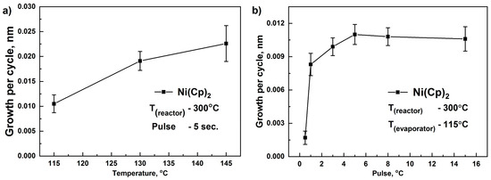
Figure 1.
The change of growth per cycle (GPC) with: (a) an increase in the evaporation temperature of NiCp2; and (b) pulse time. Substrate temperature was 300 °C. Error bars indicate the thickness gradient.
To determine the necessary pulse time to achieve saturation, GPC dependence on the pulse time of NiCp2 was studied. The experiments were performed at a reactor temperature of 300 °C. Increasing the pulse time in the range of 0.5–1 s sharply increased GPC. When the pulse time increased beyond 5 s, the GPC remained virtually unchanged. Thus, to saturate the surface of the substrate, applying a NiCp2 pulse for 5 s was sufficient.
To determine the ALD window, the dependences of GPC on temperature were studied (Figure 2a). With an increase in temperature from 150 to 200 °C, an increase in GPC was observed, indicating an insufficient reactivity of the NiCp2 in this temperature range. In the range of 200–300 °C, GPC was remained practically unchanged and was approximately 0.011–0.012 nm. This interval can be regarded as an ALD window. A further increase in temperature in the range of 300–400 °C led to an increase in the GPC of NiO, attributed to the partial decomposition of NiCp2.
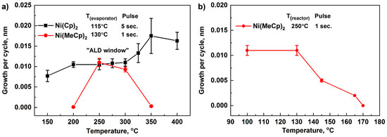
Figure 2.
GPC as a function of the deposition temperature for NiCp2, Ni(MeCp)2, and O2 plasma (a) and GPC as a function of the Ni(MeCp)2 container temperature (b). Error bars indicate the thickness gradient.
When using Ni(MeCp)2 as a reagent, an increase in the container temperature in the range of 100–130 °C did not affect the value of GPC (Figure 2b). With an increase in the container temperature in the range of 130–170 °C, a decrease in the GPC was observed. Furthermore, the color of the reagent changed from dark green to black, which was caused by the decomposition of Ni(MeCp)2 while operating in this temperature range. For further research, we used 130 °C. An increase in the pulse time from 1 to 3 s (container temperature (Tc)–130 °C, reactor temperature (Tr)–250 °C) did not affect the GPC; consequently, a pulse time of 1 s was used. When studying the effect of deposition temperature in the range of 200–350 °C, it was found that a noticeable film growth (GPC of about 0.01 nm) was observed in the range of 250–300 °C (Figure 2a). This GPC turned out to be lower than the observed GPC (0.048–0.084 nm) during the ALD of NiO films on W, Ru, Pt substrates, using direct oxygen plasma [49]. Apparently, the low growth rate is associated with the lower reactivity of the removed plasma used in our process.
Under the considered ALD conditions, the growth rates for both NiCp2 and Ni(MeCp)2 precursors were ~0.01 nm/cycle. The determined value is in the interval from 0.004 nm/cycle [47] (counter-reagent H2O) to 0.12 nm/cycle [29] (counter-reagent O3) observed for NiO deposition when Ni(Cp)2, and its derivatives were used as the precursors. Since the size of cyclopentadienyl and methylcyclopentadienyl ligands in precursor molecules are relatively high, and thus the concentration of adsorbed molecules on the surface during chemisorption due to steric hindrance [64] is not sufficient to provide the subsequent formation of NiO monolayer during the full ALD cycle.
Considering the reported values of GPC for different counter reagents (Table 1) and results of the present study as a first approximation we assume that GPC increases among the series of counter-reagents: H2O, O2 remote plasma, O2 direct plasma, and O3. However, a more detailed research is needed a since GPC depends on many factors [65]: precursor size, chemical activity, surface species, deposition temperature, etc.
Based on the obtained experimental data, NiCp2 and Ni(MeCp)2 decompose during prolonged exposure at high temperatures (more than 115 and 130 °C, respectively). However, NiCp2 is more thermostable, because for 6000–7000 cycles of ALD (about 50–60 h), a reagent pulse was observed, comparing to Ni(MeCp)2 decomposed after 2500–3000 cycles of ALD (20–25 h). In addition, when using NiCp2, there is a wider ALD window (200–300 °C). Given the better thermal stability and a wider range of deposition temperatures, the use of NiCp2 is more preferable in comparison with Ni(MeCp)2 for deposition of NiO nanofilms by ALD.
3.2. Structure and Composition of the Films Deposited on Silicon
Figure 3a shows a surface sensitive grazing incidence XRD (GIXRD) pattern of NiO film deposited on a silicon substrate using NiCp2 and oxygen plasma at 300 °C as a result of 2300 ALD cycles. The XRD pattern clearly shows reflections (111), (002), (022), (311), corresponding to cubic Fm3m modifications of NiO, as well as the reflection (311) associated with the imperfection of a single crystal of silicon [29]. The NiO cell parameter calculated by the Rietveld method was a = 0.416 nm, which is similar to the bulk value of NiO—0.418 nm (ICSD file no. 61324 (2006)). The high ratio of the intensity of reflections compared with the background indicates either the absence of the amorphous phase or its fraction is insignificant. The texture was refined using the Rietveld method and the March–Dollase parameter in the (111) direction was 0.79, which is close to 1 and it corresponds to low texturing. Lu et al. showed [29] that in the case of ALD using NiCp2, Ni(EtCp)2, and O3 (Tr = 200–300 °C) on a silicon substrate (Si (100) with etched native SiO2 layer), a cubic NiO phase is formed, but neither texture nor anisotropic strain distribution was observed. In addition, oriented growth of crystalline NiO on silicon with (in the present paper) or without a native layer of silicon oxide probably does not occur, unlike the cases when Pt [49], soda lime glass [20], MgO [51], and Al2O3 [51] are used as substrates (Table 1).
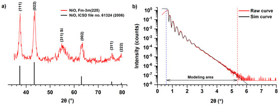
Figure 3.
GIXRD (a) and XRR (b) patterns for NiO thin film deposited on silicon substrates using NiCp2 and O2 plasma at 300 °C during 2300 ALD cycles.
According to ellipsometry and XRR (Figure 3b), the film is smooth (roughness less than 1 nm for a sample 28–30 nm in thickness) and consists of a homogeneous layer with a clear NiO/substrate interface and a slight thickness gradient (~2 nm) across the silicon substrate. The simulated curve (Figure 3b) was obtained by a simplex method using the software LEPTOS 7.7. The film density, determined on the basis of XRR curve treatment, is about 6.6 g/cm3 (Table 2), which is close to the values for bulk NiO of 6.72 g/cm3 [66]. The linear appearance of the XRR curve is probably caused by the presence of a thin layer of SiO2 on the surface of the silicon substrate. The χ2 value for the modeled curve was 8.080 × 10⁻³. It should be noted that the density of nanofilms obtained by the ALD can differ significantly from the bulk phases because of steric factors (distribution of hydroxyl groups, size of the precursor) [67] as well as a larger volume fraction of defective areas (sub-surface layer).
Table 2.
Results of XRR data treatment for sample deposited using NiCp2 at 300 °C and 2300 ALD cycles.
XPS spectra of the deposited NiO films were measured to study the elemental composition, bonding states, and conformality. Prior to the XPS measurements, the as-deposited NiO films were etched for 30 s by argon ions to remove the outermost layers. Only nickel (~47%), oxygen (~41%), and carbon (~12%) were detected (Figure 4a). Ni/O ratio was 1.15. The excess of nickel and the presence of carbon may be due to the unreacted NiCp2 molecules. No evidence of silicon was detected, so the resulting film can be considered continuous and conformal.
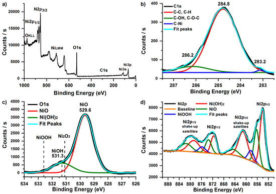
Figure 4.
XPS survey (a), C1s (b), O1s (c), and Ni2p (d) spectra of NiO thin film deposited on silicon substrates using NiCp2 and O2 plasma at 300 °C during 2300 ALD cycles.
For a detailed study of the bonding states of the film Ni2p, O1s, and C1s spectra were analyzed (Figure 4b–d). Unfortunately, the quantitative chemical analysis of Ni-containing materials is challenging because of the complexity of the Ni2p peak shapes resulting from multiplet splitting, shake-up, and plasmon loss structures [68,69]. The obtained Ni2p spectrum contains Ni2p3/2 and Ni2p1/2 peaks. Both of them can be well separated into five components using the Gaussian–Lorentzian function (Figure 4d). The most intensive peaks at 853.9 and 871.5 eV and corresponding satellite peaks (861.1 and 878.7 eV) belong to Ni2p3/2 and Ni2p1/2, respectively, which agrees with reported values of NiO [70]. The Ni2p3/2 (856.3 eV) and Ni2p1/2 (873.8 eV) peaks and their corresponding satellite peaks (864.8 and 881.5 eV) belong to Ni(OH)2 [71]. The Ni2p3/2 (858.3 eV) and Ni2p1/2 (875.8 eV) peaks probably correspond to NiOOH. Ni–OH was detected at O1s (peak at 531.3 eV), as shown in Figure 4c, and no Ni2O3 was detected in O1s and Ni2p3/2 spectra [72]. Carbon is present in the film even after argon etching. The most intensive peak at 284.8 eV (Figure 4b) corresponds to C–C and C–H of Cp ligand of residues of Ni(Cp)2 precursor. Furthermore, C–OH/C–O–C (286.2 eV) and Ni–C (283.2 eV) [73] were detected.
Thus, the film contains predominantly NiO. However, NiCp2 residues (C–C, C–H, and Ni–C bonds) and Ni(OH)2/NiOOH oxide were also present in a small amount.
On the SEM images (Figure 5a,b) of the surface of the deposited NiO film, there were no visible structures or defects. The film was smooth, uniform, and conformal. The film thickness determined from cross-sectional SEM images varied in the range of 27–31 nm (Figure 5b), which was in good agreement with the thicknesses determined using spectroscopic ellipsometry and XRR.
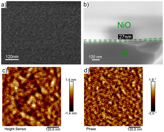
Figure 5.
Plan-view and cross-sectional SEM images (a,b), AFM topography and phase contrast images (c,d) of NiO nanofilms deposited by ALD on silicon substrates using NiCp2 and O2 plasma at 300 °C during 2300 ALD cycles.
AFM topography (Figure 5c) and phase contrast (Figure 5d) images of the surfaces of NiO films, measures in different areas (0.5 μm × 0.5 μm, 1 μm × 1 μm, and 1.5 μm × 1.5 μm) were similar. The roughness values (Ra), determined for the 0.5 μm × 0.5 μm and 1.5 μm × 1.5 μm scan areas, were 0.32 and 0.34 nm, respectively. The calculated roughness is close to the values of the silicon substrate (0.30 nm) and the amorphous (<0.39 nm [41,48]) or crystalline (<1 nm [50]) films prepared by ALD. A larger roughness value (0.63 nm), determined by the XRR method, may be caused with a larger surface area of measurement.
AFM topography and phase contrast images contain two phases (light and dark areas with diameter 10–40 nm). The lateral size of these areas on the phase contrast images was smaller than on the images of the topography. The observed phase contrast can be caused by the formation of the phases with different crystallographic orientations in substrate planes or by the presence of carbon on the surface.
3.3. Morphology of the Films Deposited on Stainless Steel
To further study the electrochemical characteristics of ALD NiO films, we deposited films on stainless-steel substrates using NiCp2 and O2 plasma. The temperature of 300 °C and 400 or 2300 cycles were used. Figure 6 shows the AFM surface topography, adhesion force maps (characterizing the interaction between the AFM probe and the sample surface) and the conductivity images for stainless-steel substrates and substrates with NiO film deposited using 400 ALD cycles. The deposition of the film did not change the surface morphology (Figure 6a,b). There was only a slight smoothing of the topography. Thus, NiO film probably had a slight tendency to grow more intensively in the grooves of the substrate. A slight contrast on the adhesion map of the stainless steel can be caused by a roughness; in deeper areas, the interaction force between the AFM probe and the surface was higher (Figure 6c). After deposition of the NiO film, the lateral difference between the adhesive forces (i.e., the forces required to detach the probe from the surface) became more significant (Figure 6d). On the map of the adhesion forces of the sample with a NiO film, a structure with pronounced contrast and clearly defined boundaries was traced (lateral size about 50 nm), which apparently indicates the presence of two phases. In addition, the adhesion forces images of steel with a NiO film (Figure 6d) showed structures with clear contrast and borders (lateral size about 50 nm). The presence of two phases can be explained by the semi-crystal structure of the film, in which ordered crystalline phases are present along with amorphous regions [74].
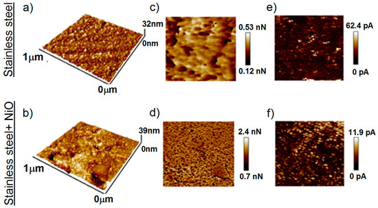
Figure 6.
AFM 3D surface topographies adhesion maps (a,b); conductivity maps (c,d); and surface electrical conductivity (e,f) of stainless-steel substrate and NiOx nanofilm deposited on a stainless-steel substrate.
Because NiO is a semiconductor, its deposition leads to the expected reduction in current amplitude (surface electrical conductivity, Figure 6c,f). At the same time, the concentration of the regions with the maximum conductivity over the sample surface increases (Figure 6f). This change can positively affect the electrochemical activity of the coating. The presence of regions with increased conductivity (lateral size of about 50 nm) can be caused by the presence of carbon in the structure or on the film surface.
3.4. Electrochemical Properties of the Films Deposited on Stainless Steel
The initial stainless steel (316SS) and stainless steel with NiO coating (Tr = 300 °C, 2300 ALD cycles) were studied with the use of cyclic voltammetry. During the investigation of stainless steel, a moderate current increase was observed (Figure 7a curves with circle and plus markers). The shape of cathode and anode curves of stainless steel with deposited NiO film (solid and dashed lines) differed from the initial substrate. The stronger increase of current in areas characterizing the performance of NiO (1.5–0.05 V (anode area) and in 1.3–2.7 V (cathode area) was observed. During the first cathode scan of NiO film, a pronounced increment of current appeared in the 0.8–0.2 V range that was caused [75] by two processes. The first was a partial reduction in organic solvents (ethylene carbonate, propylene carbonate, diethyl carbonate, ethyl methyl carbonate) and functional additives (vinylene carbonate) of electrolytes. The reduction process led to the formation of a gel-like solid electrolyte interface (SEI) film comprising LiF, Li2CO3, and other compounds on the active layer (NiO) [76]. The second process was the NiO conversion reaction with lithium as shown in Equation (2) [77]:
NiO + 2Li+ + 2e− → Ni + Li2O,
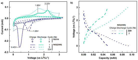
Figure 7.
Cyclic voltammograms of stainless steel 316SS and stainless steel with NiO film (a), and charge/discharge curves of stainless steel with NiO film (b).
Two peaks were observed on the anode curve. The most intense (maximum position 2.2 V) characterizes nickel oxidation (Equation (3)), which provided the main capacity of the coating under investigation. An appearance of the second maximum of current amplification at 1.6 V is related to additional pseudo-capacity which is caused by the partial decomposition of the gel-like lithium-containing film [78]. The initial compounds (Ni, Li2O, SEI film) and reactions occurred for the first five anode scans are the same consequently the position of peaks and their intensity should remain the same. The almost complete absence of changes in anode curve form indicates stable performance and retention of electrical contact between NiO and the substrate during cycling.
Ni + Li2O → NiO + 2Li+ + 2e−,
During the second scan the maximum cathode current increment shifts to higher potentials (≈1V), its intensity diminishes. Observed peak characterizes the interaction between lithium and NiO coated by SEI film, therefore, the reaction during the second scan differs from the first one. The calculated value of oxidation-reduction potential for NiO conversion reaction is equal to 1.79 V [79]. Thus, a shift of cathode current maximum from 0.41V to 1V indicates a decrease of polarization. During subsequent scans (3–5), the shape of cathode curves was similar to the shape of the cathode curve observed for the second scan. That indicates the occurrence of the same processes during 2–5 scans (cycles of charge/discharge).
The shape of cathode and anode curves and their evolution during the first five cycles characterizing the behavior of the deposited NiO film in conversion reaction with lithium is similar to results reported earlier for bulk NiO [75,80].
The shape of the charge/discharge curves of the tested thin film is similar to the shape of curves characterizing the interaction of bulk NiO with Li+ [75,80]. Because the current increase in the anode area for initial stainless steel was negligible (Figure 7a), the discharge capacity of modified steel is related to processes occurring with NiO coating. The initial measured discharge capacity of NiO film was 50 μAh. Based on film thickness (28–30 nm), density (6.6 g/cm3), and tested sample diameter (1.58 cm), the specific capacity was calculated and amounted to 1336–1379 mAh/g (≈20.4 μA/cm2). The obtained value exceeded the theoretical value stated for NiO (718 mAh/g) [6,81]. Similar discharge capacity values were reported earlier (1240 mAh/g [81] and 1256 mAh/g [82]), and excess can be caused by contributions of pseudo-capacity to the measured value. The estimated value of NiO film weight was 38 μg, and the specific discharge current was 1050 mA/g (0.8–0.9 C). With an increase of charge/discharge cycles from 6 to 223, the shape of observed curves U(C) was similar to each other but the discharge capacity augmented.
To understand the cause of the capacity increase, CV measurements were repeated after 223 cycles. The intensity of cathode maximum diminished (less lithium and NiO participate in conversion Equation (2)), and moved forward low voltages (0.8V)., thereby leading to an increase in polarization. When comparing the 5th and 224th cathode scan curves, one can note the increase of current in 0.01–0.6 V area that might be related to the insertion of lithium to SEI film. Although two anode peaks were observed at 224 discharge, almost in the same positions (1.7 V and 2.2 V), the ratio of maximum intensities changed. The amplitude of current at 1.7 V became more pronounced and surpassed the amplitude of the current at 2.2 V. Therefore, augmentation of discharge capacity during cycling was caused by the increase of pseudo-capacity provided by gel-like lithium-containing SEI film.
4. Conclusions
- Nanofilms of NiO were successfully obtained by ALD using Ni(MeCp)2, NiCp2, and oxygen plasma as counter-reagents.
- The optimal temperature range for ALD using NiCp2 was 200–300 °C, while using Ni(MeCp)2, the range is much narrower and is 250–300 °C. Growth per cycle for both precursors was 0.011–0.012 nm. Thus, NiCp2 is more thermally stable than Ni(MeCp)2, has a wider ALD window, and as a result is more suitable for the deposition of NiO films.
- The films deposited using NiCp2 (300 °C, 2300 ALD cycles) are continuous and uniform, consist of cubic modification Fm3m of NiO, and have low roughness (0.3–0.63 nm) and high density (6.6 g/cm3).
- The film contains predominantly NiO. However, carbon as cyclopentadienyl residues and Ni(OH)2/NiOOH oxide are also present in small amounts.
- The specific discharge capacity (1336–1379 mAh/g) of nickel oxide films deposited on steel substrates significantly exceeded the theoretical capacity of bulk NiO (718 mAh/g). Moreover, with repeated cycling, capacity increased. Based on the experimental data, we assume that such a high capacity is formed by the conversion capacity (reduction and oxidation of NiO) and pseudo-capacity due to the formation of a gel-like SEI film.
Author Contributions
Conceptualization, Y.K., D.N., and M.M.; Methodology, I.E. and M.M.; Validation, Y.K., D.N., and M.M.; Formal Analysis, I.M. and A.R.; Investigation, I.E., D.N., A.K., A.R., and O.L.; Resources, A.P. and M.M.; Data Curation, Y.K., D.N., and M.M.; Writing—Original Draft Preparation, Y.K., D.N., and M.M.; Writing—Review and Editing, Y.K., D.N., and M.M.; Visualization, D.N., Y.K., and I.M.; Supervision, M.M.; Project Administration, M.M.
Funding
The research was conducted under the financial support the Russian Science Foundation grant (project No. 18-73-10015).
Acknowledgments
This research was conducted using the equipment of the resource centers of the Research Park of the St. Petersburg State University «Innovative Technologies of Composite Nanomaterials», «Physical Methods of Surface Investigation», «X-ray Diffraction Studies» and «Nanotechnology».
Conflicts of Interest
The authors declare no conflict of interest.
References
- Nardi, K.L.; Yang, N.Y.; Dickens, C.F.; Strickler, A.L.; Bent, S.F. Creating highly active atomic layer deposited nio electrocatalysts for the oxygen evolution reaction. Adv. Energy Mater. 2015, 5, 10. [Google Scholar] [CrossRef]
- Patella, B.; Sunseri, C.; Inguanta, R. Nanostructured based electrochemical sensors. J. Nanosci. Nanotechnol. 2019, 19, 3459–3470. [Google Scholar] [CrossRef]
- Kerli, S.; Alver, U. Preparation and characterisation of ZnO/NiO nanocomposite particles for solar cell applications. J. Nanotechnol. 2016, 5. [Google Scholar] [CrossRef]
- Sugiyama, I.; Shibata, N.; Wang, Z.C.; Kobayashi, S.; Yamamoto, T.; Ikuhara, Y. Ferromagnetic dislocations in antiferromagnetic nio. Nat. Nanotechnol. 2013, 8, 266–270. [Google Scholar] [CrossRef]
- Nilsen, O.; Miikkulainen, V.; Gandrud, K.B.; Ostreng, E.; Ruud, A.; Fjellvag, H. Atomic layer deposition of functional films for Li-ion microbatteries. Phys. Status Solidi A Appl. Mater. Sci. 2014, 211, 357–367. [Google Scholar] [CrossRef]
- Poizot, P.; Laruelle, S.; Grugeon, S.; Dupont, L.; Tarascon, J.M. Nano-sized transition-metaloxides as negative-electrode materials for lithium-ion batteries. Nature 2000, 407, 496–499. [Google Scholar] [CrossRef]
- Maximov, M.Y.; Novikov, P.A.; Nazarov, D.V.; Rymyantsev, A.M.; Silin, A.O.; Zhang, Y.; Popovich, A.A. Characterization and electrochemical performance at high discharge rates of tin dioxide thin films synthesized by atomic layer deposition. J. Electron. Mater. 2017, 46, 6571–6577. [Google Scholar] [CrossRef]
- Reddy, M.V.; Rao, G.V.S.; Chowdari, B.V.R. Metal oxides and oxysalts as anode materials for Li ion batteries. Chem. Rev. 2013, 113, 5364–5457. [Google Scholar] [CrossRef]
- Chen, J.S.; Lou, X.W. SnO2-based nanomaterials: Synthesis and application in lithium-ion batteries. Small 2013, 9, 1877–1893. [Google Scholar] [CrossRef] [PubMed]
- Chen, X.; Zhang, N.Q.; Sun, K.N. Facile ammonia-induced fabrication of nanoporous nio films with enhanced lithium-storage properties. Electrochem. Commun. 2012, 20, 137–140. [Google Scholar] [CrossRef]
- Wang, Y.X.; Liu, B.; Li, Q.Y.; Cartmell, S.; Ferrara, S.; Deng, Z.Q.D.; Xiao, J. Lithium and lithium ion batteries for applications in microelectronic devices: A review. J. Power Sources 2015, 286, 330–345. [Google Scholar] [CrossRef]
- Ukoba, K.O.; Eloka-Eboka, A.C.; Inambao, F.L. Review of nanostructured nio thin film deposition using the spray pyrolysis technique. Renew. Sust. Energ. Rev. 2018, 82, 2900–2915. [Google Scholar] [CrossRef]
- George, S.M. Atomic layer deposition: An overview. Chem. Rev. 2010, 110, 111–131. [Google Scholar] [CrossRef]
- Miikkulainen, V.; Leskela, M.; Ritala, M.; Puurunen, R.L. Crystallinity of inorganic films grown by atomic layer deposition: Overview and general trends. J. Appl. Phys. 2013, 113, 101. [Google Scholar] [CrossRef]
- Profijt, H.B.; Potts, S.E.; van de Sanden, M.C.M.; Kessels, W.M.M. Plasma-assisted atomic layer deposition: Basics, opportunities, and challenges. J. Vac. Sci. Technol. A 2011, 29, 26. [Google Scholar] [CrossRef]
- Liu, J.; Zhu, H.; Shiraz, M.H.A. Toward 3D solid-state batteries via atomic layer deposition aproach. Front. Energy Res. 2018, 6, 10. [Google Scholar]
- Lindblad, M.; Lindfors, L.P.; Suntola, T. Preparation of Ni/Al2O3 catalysts from vapor-phase by atomic layer epitaxy. Catal. Lett. 1994, 27, 323–336. [Google Scholar] [CrossRef]
- Jacobs, J.P.; Lindfors, L.P.; Reintjes, J.G.H.; Jylha, O.; Brongersma, H.H. The growth-mechanism of nickel in the preparation of Ni/Al2O3 catalysts studied by LEIS, XPS and catalytic activity. Catal. Lett. 1994, 25, 315–324. [Google Scholar] [CrossRef]
- Maki-Arvela, P.; Tiainen, L.P.; Lindblad, M.; Demirkan, K.; Kumar, N.; Sjoholm, R.; Ollonqvist, T.; Vayrynen, J.; Salmi, T.; Murzin, D.Y. Liquid-phase hydrogenation of citral for production of citronellol: Catalyst selection. Appl. Catal. A Gen. 2003, 241, 271–288. [Google Scholar] [CrossRef]
- Utriainen, M.; Kroger-Laukkanen, M.; Niinisto, L. Studies of nio thin film formation by atomic layer epitaxy. Mater. Sci. Eng. B Solid State Mater. Adv. Technol. 1998, 54, 98–103. [Google Scholar] [CrossRef]
- Bratvold, J.E.; Fjellvag, H.; Nilsen, O. Atomic layer deposition of oriented nickel titanate (NiTiO3). Appl. Surf. Sci. 2014, 311, 478–483. [Google Scholar] [CrossRef]
- Shim, J.W.; Fuentes-Hernandez, C.; Dindar, A.; Zhou, Y.H.; Khan, T.M.; Kippelen, B. Polymer solar cells with NiO hole-collecting interlayers processed by atomic layer deposition. Org. Electron. 2013, 14, 2802–2808. [Google Scholar] [CrossRef]
- Nam, W.J.; Gray, Z.; Stayancho, J.; Plotnikov, V.; Kwon, D.; Waggoner, S.; Shenai-Khatkhatec, D.V.; Pickering, M.; Okano, T.; Compaan, A.; et al. ALD NiO thin films as a hole transport-electron blocking layer material for photo-detector and solar cell devices. Ecs Trans. 2015, 66, 275–279. [Google Scholar] [CrossRef]
- Li, H.; Perera, T.; Shenai, D.V.; Li, Z.; Gordon, R.G. New Ni amidinate source for ALD/CVD of NiNx, NiO and Ni. In Proceedings of the 11th International Conference on Atomic Layer Deposition, Cambridge, MA, USA, 26–29 June 2011. [Google Scholar]
- Chae, J.; Park, H.S.; Kang, S.W. Atomic layer deposition of nickel by the reduction of preformed nickel oxide. Electrochem. Solid State Lett. 2002, 5, C64–C66. [Google Scholar] [CrossRef]
- Kim, D.H.; Sim, J.K.; Lee, J.; Seo, H.O.; Jeong, M.G.; Kim, Y.D.; Kim, S.H. Carbon dioxide reforming of methane over mesoporous Ni/SiO2. Fuel 2013, 112, 111–116. [Google Scholar] [CrossRef]
- Jeong, M.G.; Kim, D.H.; Lee, S.K.; Lee, J.H.; Han, S.W.; Park, E.J.; Cychosz, K.A.; Thommes, M.; Hwang, Y.K.; Chang, J.S.; et al. Decoration of the internal structure of mesoporous chromium terephthalate MIL-101 with NiO using atomic layer deposition. Microporous Mesoporous Mat. 2016, 221, 101–107. [Google Scholar] [CrossRef]
- Wang, G.Z.; Gao, Z.; Wan, G.P.; Lin, S.W.; Yang, P.; Qin, Y. High densities of magnetic nanoparticles supported on graphene fabricated by atomic layer deposition and their use as efficient synergistic microwave absorbers. Nano Res. 2014, 7, 704–716. [Google Scholar] [CrossRef]
- Lu, H.L.; Scarel, G.; Wiemer, C.; Perego, M.; Spiga, S.; Fanciulli, M.; Pavia, G. Atomic layer deposition of NiO films on Si(100) using cyclopentadienyl-type compounds and ozone as precursors. J. Electrochem. Soc. 2008, 155, H807–H811. [Google Scholar] [CrossRef]
- Wang, G.Z.; Peng, X.G.; Yu, L.; Wan, G.P.; Lin, S.W.; Qin, Y. Enhanced microwave absorption of ZnO coated with Ni nanoparticles produced by atomic layer deposition. J. Mater. Chem. A 2015, 3, 2734–2740. [Google Scholar] [CrossRef]
- Gao, Z.; Dong, M.; Wang, G.Z.; Sheng, P.; Wu, Z.W.; Yang, H.M.; Zhang, B.; Wang, G.F.; Wang, J.G.; Qin, Y. Multiply confined nickel nanocatalysts produced by atomic layer deposition for hydrogenation reactions. Angew. Chem. Int. Ed. 2015, 54, 9006–9010. [Google Scholar] [CrossRef]
- Alburquenque, D.; Del Canto, M.; Arenas, C.; Tejo, F.; Pereira, A.; Escrig, J. Dewetting of Ni thin films obtained by atomic layer deposition due to the thermal reduction process: Variation of the thicknesses. Thin Solid Film. 2017, 638, 114–118. [Google Scholar] [CrossRef]
- Zhang, R.Y.; Wei, H.H.; Si, W.J.; Ou, G.; Zhao, C.S.; Song, M.J.; Zhang, C.; Wu, H. Enhanced electrocatalytic activity for water splitting on NiO/Ni/carbon fiber paper. Materials 2017, 10, 8. [Google Scholar] [CrossRef] [PubMed]
- Zhang, J.K.; Chen, C.Q.; Yan, W.J.; Duan, F.F.; Zhang, B.; Gao, Z.; Qin, Y. Ni nanoparticles supported on cnts with excellent activity produced by atomic layer deposition for hydrogen generation from the hydrolysis of ammonia borane. Catal. Sci. Technol. 2016, 6, 2112–2119. [Google Scholar] [CrossRef]
- Pereira, A.; Palma, J.L.; Denardin, J.C.; Escrig, J. Temperature-dependent magnetic properties of Ni nanotubes synthesized by atomic layer deposition. Nanotechnology 2016, 27, 6. [Google Scholar] [CrossRef] [PubMed][Green Version]
- Lamperti, A.; Spiga, S.; Lu, H.L.; Wiemer, C.; Perego, M.; Cianci, E.; Alia, M.; Fanciulli, M. Study of the interfaces in resistive switching NiO thin films deposited by both ald and e-beam coupled with different electrodes (Si, Ni, Pt, W, TiN). Microelectron. Eng. 2008, 85, 2425–2429. [Google Scholar] [CrossRef]
- Spiga, S.; Lamperti, A.; Wiemer, C.; Perego, M.; Cianci, E.; Tallarida, G.; Lu, H.L.; Alia, M.; Volpe, F.G.; Fanciulli, M. Resistance switching in amorphous and crystalline binary oxides grown by electron beam evaporation and atomic layer deposition. Microelectron. Eng. 2008, 85, 2414–2419. [Google Scholar] [CrossRef]
- Huber, R.; Berberich, P.; Rapp, T.; Schwarze, T.; Grundler, D.; Bachmann, J.; Nielsch, K. Spin wave resonances in ferromagnetic thin films prepared via atomic layer deposition. In Proceedings of the Baltic ALD/GerALD Conference 2010, Hamburg, Germany, 16–17 September 2010. [Google Scholar]
- Yu, L.; Wang, G.L.; Wan, G.P.; Wang, G.Z.; Lin, S.W.; Li, X.Y.; Wang, K.; Bai, Z.M.; Xiang, Y. Highly effective synthesis of NiO/CNT nanohybrids by atomic layer deposition for high-rate and long-life supercapacitors. Dalton Trans. 2016, 45, 13779–13786. [Google Scholar] [CrossRef] [PubMed]
- Daub, M.; Knez, M.; Goesele, U.; Nielsch, K. Ferromagnetic nanotubes by atomic layer deposition in anodic alumina membranes. J. Appl. Phys. 2007, 101, 3. [Google Scholar] [CrossRef]
- Yang, T.S.; Cho, W.T.; Kim, M.; An, K.S.; Chung, T.M.; Kim, C.G.; Kim, Y. Atomic layer deposition of nickel oxide films using Ni(dmamp)2 and water. J. Vac. Sci. Technol. A 2005, 23, 1238–1243. [Google Scholar] [CrossRef]
- Yang, J.H.; Lee, S.Y.; Song, W.S.; Shin, Y.S.; Park, C.Y.; Kim, H.J.; Cho, W.; An, K.S. Field emission properties of ZnO nanorods coated with NiO film. J. Vac. Sci. Technol. B 2008, 26, 1021–1024. [Google Scholar] [CrossRef]
- So, B.S.; You, Y.H.; Kim, K.H.; Hwang, J.; Cho, W.; Lee, S.S.; Chung, T.M.; Lee, Y.K.; Kim, C.G.; An, K.S.; et al. Crystallization of amorphous silicon thin films using self-limiting ALD of nickel oxide. Electrochem. Solid State Lett. 2007, 10, J61–J64. [Google Scholar] [CrossRef]
- You, Y.H.; So, B.S.; Hwang, J.H.; Cho, W.; Lee, S.S.; Chung, T.M.; Kim, C.G.; An, K.S. Impedance spectroscopy characterization of resistance switching NiO thin films prepared through atomic layer deposition. Appl. Phys. Lett. 2006, 89, 3. [Google Scholar] [CrossRef]
- Lu, H.L.; Scarel, G.; Li, X.L.; Fanciulli, M. Thin MnO and NiO films grown using atomic layer deposition from ethylcyclopentadienyl type of precursors. J. Cryst. Growth 2008, 310, 5464–5468. [Google Scholar] [CrossRef]
- Pore, V.; Tois, E.; Matero, R.; Haukka, S.; Tuominen, M.; Woodruff, J.; Milligan, B.; Tang, F.; Givens, M. Nickel silicide for source-drain contacts from ALD NiO films. In Proceedings of the 2015 IEEE International Interconnect Technology Conference and 2015 IEEE Materials for Advanced Metallization Conference (IITC/MAM), Grenoble, France, 18–21 May 2015. [Google Scholar]
- Dashjav, E.; Lipinska-Chwalek, M.; Gruner, D.; Mauer, G.; Luysberg, M.; Tietz, F. Atomic layer deposition and high-resolution electron microscopy characterization of nickel nanoparticles for catalyst applications. Surf. Coat. Technol. 2016, 307, 428–435. [Google Scholar] [CrossRef]
- Kumagai, H.; Matsumoto, M.; Toyoda, K.; Obara, M. Preparation and characteristics of nickel oxide thin film by controlled growth with sequential surface chemical reactions. J. Mater. Sci. Lett. 1996, 15, 1081–1083. [Google Scholar] [CrossRef]
- Song, S.J.; Lee, S.W.; Kim, G.H.; Seok, J.Y.; Yoon, K.J.; Yoon, J.H.; Hwang, C.S.; Gatineau, J.; Ko, C. Substrate dependent growth behaviors of plasma-enhanced atomic layer deposited nickel oxide films for resistive switching application. Chem. Mater. 2012, 24, 4675–4685. [Google Scholar] [CrossRef]
- Lindahl, E.; Ottosson, M.; Carlsson, J.O. Atomic layer deposition of NiO by the Ni(thd)2/H2O precursor combination. Chem. Vap. Depos. 2009, 15, 186–191. [Google Scholar] [CrossRef]
- Lindahl, E.; Lu, J.; Ottosson, M.; Carlsson, J.O. Epitaxial NiO (100) and NiO (111) films grown by atomic layer deposition. J. Cryst. Growth 2009, 311, 4082–4088. [Google Scholar] [CrossRef]
- Lindahl, E.; Ottosson, M.; Carlsson, J.O. Growth and stability of CVD Ni3N and ALD NiO dual layers. Surf. Coat. Technol. 2010, 205, 710–716. [Google Scholar] [CrossRef]
- Hagen, D.J.; Tripathi, T.S.; Karppinen, M. Atomic layer deposition of nickel-cobalt spinel thin films. Dalton Trans. 2017, 46, 4796–4805. [Google Scholar] [CrossRef] [PubMed]
- Seim, H.; Molsa, H.; Nieminen, M.; Fjellvag, H.; Niinisto, L. Deposition of LaNiO3 thin films in an atomic layer epitaxy reactor. J. Mater. Chem. 1997, 7, 449–454. [Google Scholar] [CrossRef]
- Nazarov, D.V.; Maximov, M.Y.; Novikov, P.A.; Popovich, A.A.; Silin, A.O.; Smirnov, V.M.; Bobrysheva, N.P.; Osmolovskaya, O.M.; Osmolovsky, M.G.; Rumyantsev, A.M. Atomic layer deposition of tin oxide using tetraethyltin to produce high-capacity Li-ion batteries. J. Vac. Sci. Technol. A 2017, 35, 11. [Google Scholar] [CrossRef]
- Blasco, N.; Girard, J.M. Recent development of ligand chemistries for next generation conformal peald/ald of metal & oxides. In Proceedings of the ALD Workshop on Atomic Layer Processing @ Semicon Europa, Grenoble, France, 7–10 October 2014. [Google Scholar]
- Vieyra-Eusebio, M.T.; Rojas, A. Vapor pressures and sublimation enthalpies of nickelocene and cobaltocene measured by thermogravimetry. J. Chem. Eng. Data 2011, 56, 5008–5018. [Google Scholar] [CrossRef]
- Ishikawa, M.; Kada, T.; Machida, H.; Ohshita, Y.; Ogura, A. Ni precursor for chemical vapor deposition of NiSi. Jpn. J. Appl. Phys. 2004, 43, 1833–1836. [Google Scholar] [CrossRef]
- Zhao, F.Z.; Gong, M.; Cao, K.; Zhang, Y.H.; Li, J.L.; Chen, R. Atomic layer deposition of Ni on Cu nanoparticles for methanol synthesis from CO2 hydrogenation. ChemCatChem 2017, 9, 3772–3778. [Google Scholar] [CrossRef]
- Huber, R. Control of spin waves on the nanoscale in one-dimensional magnonic crystals and atomic layer deposition of metallic ferromagnets for second generation of nanomaterials. Ph.D. Thesis, Technische Universitat Munchen, München, Germany, 2013. [Google Scholar]
- Bachmann, J.; Zolotaryov, A.; Albrecht, O.; Goetze, S.; Berger, A.; Hesse, D.; Novikov, D.; Nielsch, K. Stoichiometry of nickel oxide films prepared by ALD. Chem. Vap. Depos. 2011, 17, 177–180. [Google Scholar] [CrossRef]
- Kang, J.K.; Rhee, S.W. Metalorganic chemical vapor deposition of nickel films from Ni(C5H5)2/H2. J. Mater. Res. 2000, 15, 1828–1833. [Google Scholar] [CrossRef]
- Siddiqui, R.A. Experimental investigations of thermodynamic properties of organometallic compounds. Universität Duisburg-Essen. Ph.D. Thesis, Universität Duisburg-Essen, Duisburg, Germany, 2009. [Google Scholar]
- Ylilammi, M. Monolayer thickness in atomic layer deposition. Thin Solid Film. 1996, 279, 124–130. [Google Scholar] [CrossRef]
- Puurunen, R.L. Surface chemistry of atomic layer deposition: A case study for the trimethylaluminum/water process. J. Appl. Phys. 2005, 97, 52. [Google Scholar] [CrossRef]
- Lide, D.R. CRC Handbook of Chemistry and Physics, 79th ed.; CRC Press Inc.: Boca Raton, FL, USA, 1998. [Google Scholar]
- Kraytsberg, A.; Drezner, H.; Auinat, M.; Shapira, A.; Solomatin, N.; Axmann, P.; Wohlfahrt-Mehrens, M.; Ein-Eli, Y. Atomic layer deposition of a particularized protective MgF2 film on a Li-ion battery LiMn1.5Ni0.5O4 cathode powder material. ChemNanoMat 2015, 1, 577–585. [Google Scholar]
- Biesinger, M.C.; Payne, B.P.; Lau, L.W.M.; Gerson, A.; Smart, R.S.C. X-ray photoelectron spectroscopic chemical state quantification of mixed nickel metal, oxide and hydroxide systems. Surf. Interface Anal. 2009, 41, 324–332. [Google Scholar] [CrossRef]
- Biesinger, M.C.; Payne, B.P.; Grosvenor, A.P.; Lau, L.W.M.; Gerson, A.R.; Smart, R.S. Resolving surface chemical states in XPS analysis of first row transition metals, oxides and hydroxides: Cr, Mn, Fe, Co and Ni. Appl. Surf. Sci. 2011, 257, 2717–2730. [Google Scholar] [CrossRef]
- Mansour, A.N. Characterization of NiO by XPS. Surf. Sci. Spectra 1994, 3, 232–238. [Google Scholar] [CrossRef]
- Mansour, A.N. Characterization of β-Ni(OH)2 by XPS. Surf. Sci. Spectra 1994, 3, 239–246. [Google Scholar] [CrossRef]
- Hu, H.L.; Zhu, J.G.; Chen, M.S.; Guo, T.L.; Li, F.S. Inkjet-printed p-type nickel oxide thin-film transistor. Appl. Surf. Sci. 2018, 441, 295–302. [Google Scholar] [CrossRef]
- Furlan, A.; Lu, J.; Hultman, L.; Jansson, U.; Magnuson, M. Crystallization characteristics and chemical bonding properties of nickel carbide thin film nanocomposites. J. Phys.-Condes. Matter 2014, 26, 11. [Google Scholar] [CrossRef]
- Gutierrez, J.; Mondragon, I.; Tercjak, A. Quantitative nanoelectrical and nanomechanical properties of nanostructured hybrid composites by peakforce tunneling atomic force microscopy. J. Phys. Chem. C 2014, 118, 1206–1212. [Google Scholar] [CrossRef]
- Kawamori, M.; Asai, T.; Shirai, Y.; Yagi, S.; Oishi, M.; Ichitsubo, T.; Matsubara, E. Three-dimensional nanoelectrode by metal nanowire nonwoven clothes. Nano Lett. 2014, 14, 1932–1937. [Google Scholar] [CrossRef]
- Wang, A.P.; Kadam, S.; Li, H.; Shi, S.Q.; Qi, Y. Review on modeling of the anode solid electrolyte interphase (SEI) for lithium-ion batteries. npj Comput. Mater. 2018, 4, 26. [Google Scholar] [CrossRef]
- Gao, X.P.; Yang, H.X. Multi-electron reaction materials for high energy density batteries. Energy Environ. Sci. 2010, 3, 174–189. [Google Scholar] [CrossRef]
- Laruelle, S.; Grugeon, S.; Poizot, P.; Dolle, M.; Dupont, L.; Tarascon, J.M. On the origin of the extra electrochemical capacity displayed by Mo/Li cells at low potential. J. Electrochem. Soc. 2002, 149, A627–A634. [Google Scholar] [CrossRef]
- Poizot, P.; Laruelle, S.; Grugeon, S.; Tarascon, J.M. Rationalization of the low-potential reactivity of 3d-metal-based inorganic compounds toward Li. J. Electrochem. Soc. 2002, 149, A1212–A1217. [Google Scholar] [CrossRef]
- Huang, X.H.; Tu, J.P.; Zhang, C.Q.; Zhou, F. Hollow microspheres of NiO as anode materials for lithium-ion batteries. Electrochim. Acta 2010, 55, 8981–8985. [Google Scholar] [CrossRef]
- Long, H.; Shi, T.L.; Hu, H.; Jiang, S.L.; Xi, S.; Tang, Z.R. Growth of hierarchal mesoporous NiO nanosheets on carbon cloth as binder-free anodes for high-performance flexible lithium-ion batteries. Sci. Rep. 2014, 4, 9. [Google Scholar] [CrossRef] [PubMed]
- Kong, X.W.; Zhang, R.L.; Zhong, S.K.; Wu, L. Electrospinning synthesis of 3D porous NiO nanorods as anode material for lithium-ion batteries. Mater. Sci. Pl. 2016, 34, 227–232. [Google Scholar]


© 2019 by the authors. Licensee MDPI, Basel, Switzerland. This article is an open access article distributed under the terms and conditions of the Creative Commons Attribution (CC BY) license (http://creativecommons.org/licenses/by/4.0/).