Surface Analysis and Optical Properties of Cu-Doped ZnO Thin Films Deposited by Radio Frequency Magnetron Sputtering


Abstract
:1. Introduction
2. Materials and Methods
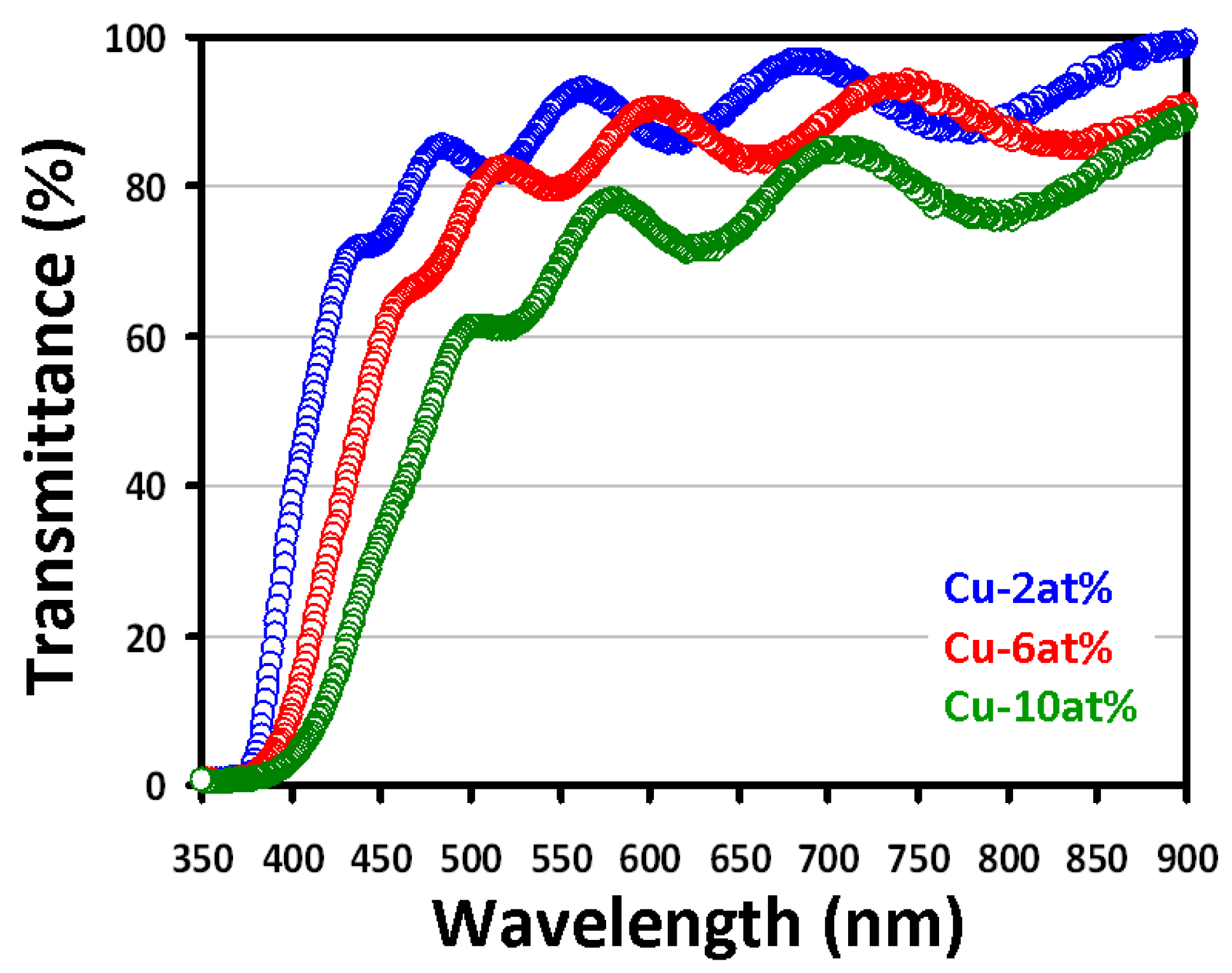
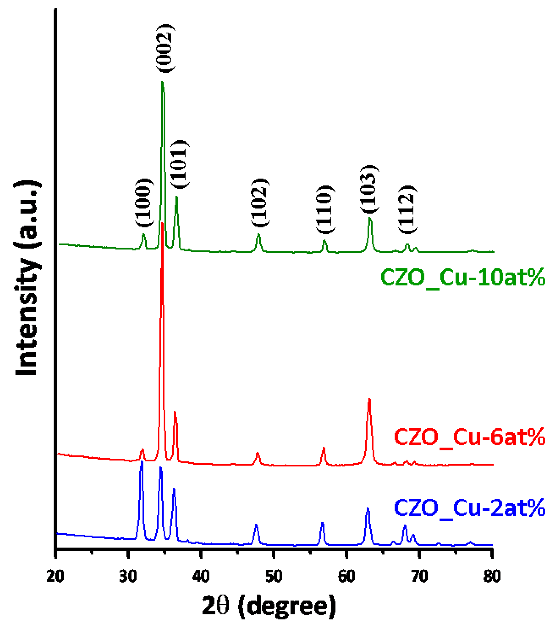
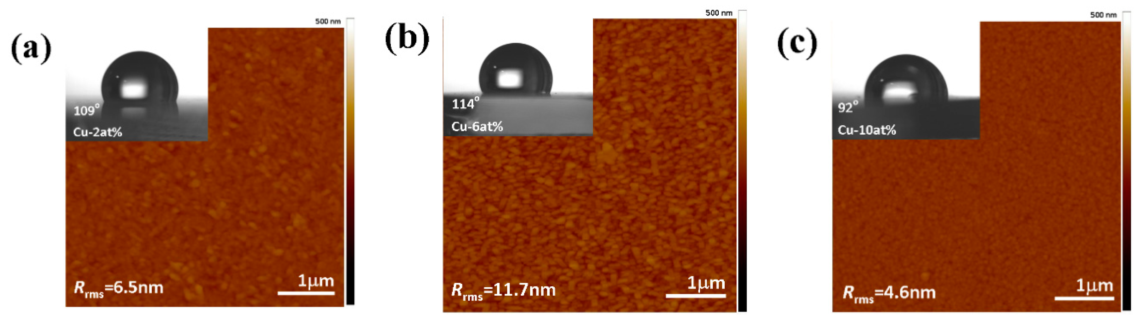
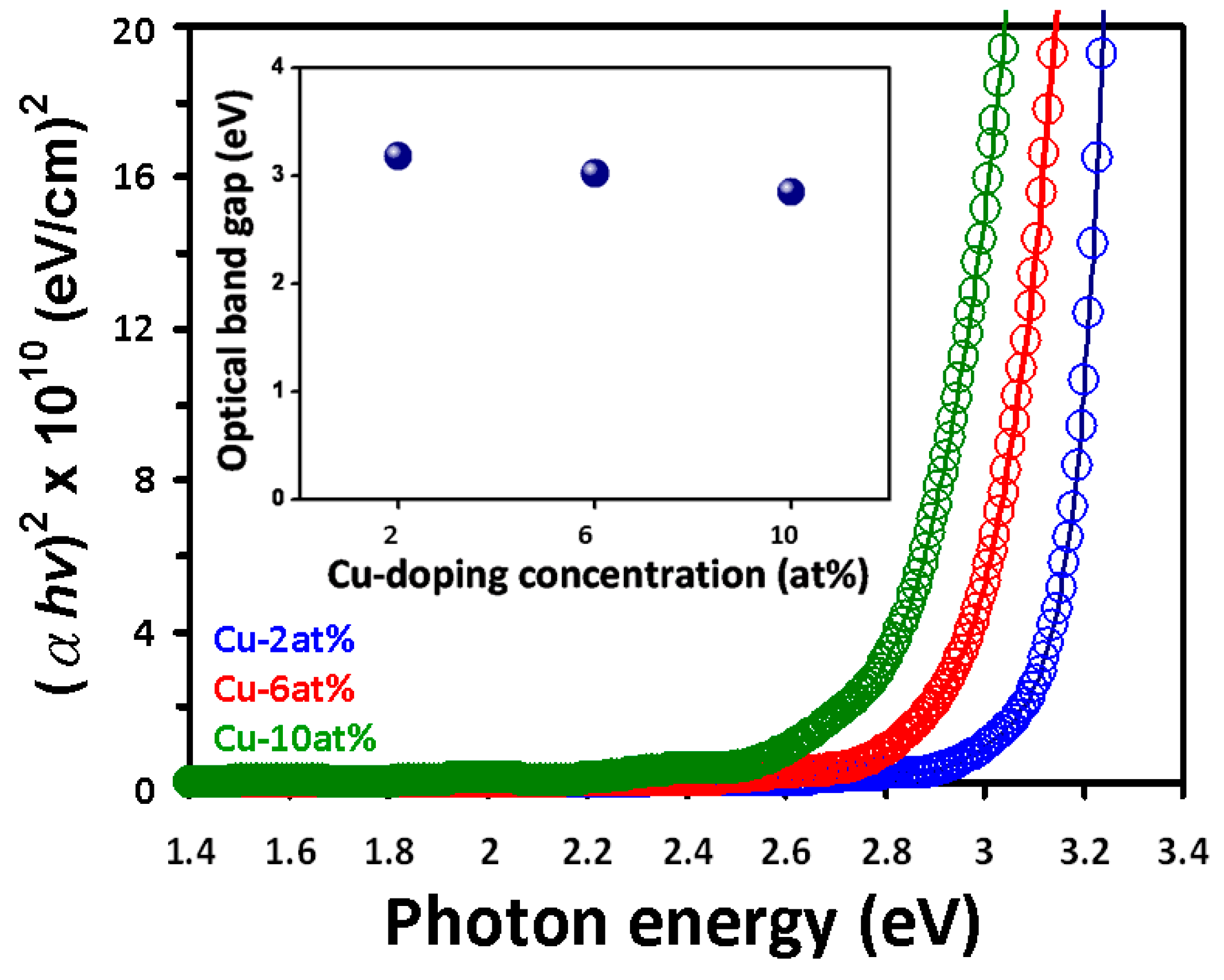
3. Results
4. Conclusions
Author Contributions
Funding
Acknowledgments
Conflicts of Interest
References
- Chu, S.; Wang, G.; Zhou, W.; Lin, Y.; Chernyak, L.; Zhao, J.; Kong, J.; Li, L.; Ren, J.; Liu, J. Electrically pumped waveguide lasing from ZnO nanowires. Nat. Nanotechnol. 2011, 6, 506–510. [Google Scholar] [CrossRef] [PubMed]
- Wang, C.F.; Ba, R.R.; Zhao, K.; Zhang, T.P.; Dong, L.; Pan, C.F. Enhanced emission intensity of vertical aligned flexible ZnO nanowire/p-polymer hybridized LED array by piezo-phototronic effect. Nano Energy 2015, 14, 364–371. [Google Scholar] [CrossRef]
- Liu, X.H.; Wang, H.Q.; Li, Y.R.; Gui, Z.Z.; Ming, S.Q.; Usman, K.; Zhang, W.J.; Fang, J.F. Regular Organic Solar Cells with Efficiency over 10% and Promoted Stability by Ligand- and Thermal Annealing-Free Al-Doped ZnO Cathode Interlayer. Adv. Sci. 2017, 4, 1700053. [Google Scholar] [CrossRef] [PubMed] [Green Version]
- Li, Y.; Yao, R.; Wang, H.H.; Wu, X.M.; Wu, J.Z.; Wu, X.H.; Qin, W. Enhanced Performance in Al-Doped ZnO Based Transparent Flexible Transparent Thin-Film Transistors Due to Oxygen Vacancy in ZnO Film with Zn–Al–O Interfaces Fabricated by Atomic Layer Deposition. ACS Appl. Mater. Interfaces 2017, 9, 11711–11720. [Google Scholar] [CrossRef] [PubMed]
- Yeh, P.H.; Li, Z.; Wang, Z.L. Schottky-Gated Probe-Free ZnO Nanowire Biosensor. Adv. Mater. 2009, 21, 4975–4978. [Google Scholar] [CrossRef] [PubMed]
- Park, C.H.; Zhang, S.B.; Wei, S.H. Origin of p-type doping difficulty in ZnO: The impurity perspective. Phys. Rev. B 2002, 66, 073202. [Google Scholar] [CrossRef]
- Look, D.C.; Jones, R.L.; Sizelove, J.R.; Garces, N.Y.; Giles, C.N.; Halliburton, L.E. The path to ZnO devices: Donor and acceptor dynamics. Phys. Status Solidi A 2003, 195, 171–177. [Google Scholar] [CrossRef]
- Look, D.C.; Clafin, B. P-type doping and devices based on ZnO. Phys. Status Solidi B 2004, 241, 624–630. [Google Scholar] [CrossRef]
- Shi, S.W.; He, G.; Zhang, M.; Song, X.P.; Li, J.L.; Wang, X.X.; Cui, J.B.; Chen, X.S.; Sun, Z.Q. Microstructural, Optical and Electrical Properties of Molybdenum Doped ZnO Films Deposited by Magnetron Sputtering. Sci. Adv. Mater. 2012, 4, 193–198. [Google Scholar] [CrossRef]
- Lee, D.J.; Kim, K.J.; Kim, S.H.; Kwon, J.Y.; Xu, J.; Kim, K.B. Atomic layer deposition of Ti-doped ZnO films with enhanced electron mobility. J. Mater. Chem. C 2013, 1, 4761–4769. [Google Scholar] [CrossRef]
- Liu, H.; Yang, J.; Hua, Z.; Zhang, Y.; Yang, L.; Xiao, L.; Xie, Z. The structure and magnetic properties of Cu-doped ZnO prepared by sol–gel method. Appl. Surf. Sci. 2010, 256, 4162–4165. [Google Scholar] [CrossRef]
- Allabergenov, B.; Chung, S.H.; Jeong, S.M.; Kim, S.; Choi, B. Enhanced blue photoluminescence realized by copper diffusion doping of ZnO thin films. Opt. Mater. Express 2013, 3, 1733–1741. [Google Scholar] [CrossRef]
- Ashokkumar, M.; Muthukumaran, S. Effect of Ni doping on electrical, photoluminescence and magnetic behavior of Cu doped ZnO nanoparticles. J. Lumin. 2015, 162, 97–103. [Google Scholar] [CrossRef]
- Iikhechi, N.N.; Ghobadi, N.; Yahyavi, F. Enhanced optical and hydrophilic properties of V and La co-doped ZnO thin films. Opt. Quant. Electron. 2017, 49, 39. [Google Scholar] [CrossRef]
- Wu, Z.F.; Wu, X.M.; Zhuge, L.J. Synthesis and magnetic properties of Cu doped ZnO nanorods via radio frequency plasma deposition. Appl. Phys. Lett. 2008, 93, 023103. [Google Scholar] [CrossRef]
- Zimmermann, J.; Reifler, F.A.; Schrade, U.; Artus, G.R.J.; Seeger, S. Long term environmental durability of a superhydrophobic silicone nanofilament coating. Colloids Surf. A Physicochem. Eng. Asp. 2007, 302, 234–240. [Google Scholar] [CrossRef]
- Tyona, M.D.; Osuji, R.U.; Asogwa, P.U.; Jambure, S.B.; Ezema, F.I. Structural modification and band gap tailoring of zinc oxide thin films using copper impurities. J. Solid State Electrochem. 2017, 21, 2629–2637. [Google Scholar] [CrossRef]
- Angelo, M.S.; McCandless, B.E.; Birkmire, R.W.; Rykov, S.A.; Chen, J.G. Contact wetting angle as a characterization technique for processing CdTe/CdS solar cells. Prog. Photovolt. 2007, 15, 93–111. [Google Scholar] [CrossRef]
- Sun, H.; Luo, M.; Weng, W.; Cheng, K.; Du, P.; Shen, G.; Han, G. Room-temperature preparation of ZnO nanosheets grown on Si substrates by a seed-layer assisted solution route. Nanotechnology 2008, 19, 125603. [Google Scholar] [CrossRef] [PubMed]
- Shinde, S.K.; Ghodake, G.S.; Dubal, D.P.; Lohar, G.M.; Lee, D.S.; Fulari, V.J. Structural, optical, and photo-electrochemical properties of marygold-like CdSe0.6Te0.4 synthesized by electrochemical route. Ceram. Int. 2014, 40, 11519–11524. [Google Scholar] [CrossRef]
- Hashim, N.H.; Subramani, S.; Devarajan, M.; Ibrahim, A.R. Structural and surface characterization of undoped ZnO and Cu doped ZnO using sol–gel spin coating method. J. Mater. Sci. Mater. Electron. 2016, 27, 3520–3530. [Google Scholar] [CrossRef]
- Suja, M.; Bashar, S.B.; Morshed, M.M.; Liu, J.L. Realization of Cu-Doped p-Type ZnO Thin Films by Molecular Beam Epitaxy. ACS Appl. Mater. Interfaces 2015, 7, 8894–8899. [Google Scholar] [CrossRef] [PubMed]
- Shewale, P.S.; Yu, Y.S. UV photodetection properties of pulsed laser deposited Cu-doped ZnO thin film. Ceram. Int. 2017, 43, 4175–4182. [Google Scholar] [CrossRef]
- Xu, S.S.; Lu, H.L.; Zhang, Y.; Wang, T.; Geng, Y.; Huang, W.; Ding, S.J.; Zhang, D.W. Bandgap narrowing and conductivity evolution of atomic-layer-deposited ZnO:Cu thin films under rapid thermal annealing. J. Alloys Compd. 2015, 638, 133–135. [Google Scholar] [CrossRef]
- Sreedhar, A.; Kwon, J.H.; Yi, J.; Kim, J.S.; Gwag, J.S. Enhanced photoluminescence properties of Cu-doped ZnO thin films deposited by simultaneous RF and DC magnetron sputtering. Mater. Sci. Semcond. Process. 2016, 49, 8–14. [Google Scholar] [CrossRef]
- Cullity, B.D.; Stock, S.R. Element of X-ray Diffraction; Prentice Hall: New Jersey, NJ, USA, 2001; p. 170. [Google Scholar]
- Ottone, C.; Lamberti, A.; Cauda, V.; Fontana, M. Wetting Behavior of Hierarchical Oxide Nanostructures: TiO2 Nanotubes from Anodic Oxidation Decorated with ZnO Nanostructures. J. Electrochem. Soc. 2014, 161, D484–D488. [Google Scholar] [CrossRef]
- Bayati, R.; Molaei, R.; Richmond, A.; Nori, S.; Wu, F.; Kumar, D.; Narayan, J.; Reynolds, J.G.; Reynolds, C.L. Modification of Properties of Yttria Stabilized Zirconia Epitaxial Thin Films by Excimer Laser Annealing. ACS Appl. Mater. Interfaces 2014, 6, 22316. [Google Scholar] [CrossRef] [PubMed]
- Dave, V.; Gupta, H.O.; Chandra, R. Nanostructured hydrophobic DC sputtered inorganic oxide coating for outdoor glass insulators. Appl. Surf. Sci. 2014, 295, 231–239. [Google Scholar] [CrossRef]
- Mahadik, D.B.; Rao, A.V.; Parale, V.G.; Kavale, M.S.; Wagh, P.B.; Ingale, S.V.; Gupta, S.C. Effect of surface composition and roughness on the apparent surface free energy of silica aerogel materials. Appl. Phys. Lett. 2011, 99, 104104. [Google Scholar] [CrossRef]
- Chi, P.W.; Wei, D.H.; Wu, S.H.; Chen, Y.Y.; Yao, Y.D. Photoluminescence and wettability control of NiFe/ZnO heterostructure bilayer films. RSC Adv. 2015, 5, 96705–96713. [Google Scholar] [CrossRef]
- Chao, C.H.; Chi, P.W.; Wei, D.H. Investigations on the Crystallographic Orientation Induced Surface Morphology Evolution of ZnO Thin Films and Their Wettability and Conductivity. J. Phys. Chem. C 2016, 120, 8210–8219. [Google Scholar] [CrossRef]
- Sapkal, R.T.; Shinde, S.S.; Babar, A.R.; Moholkar, A.V.; Rajpure, K.Y.; Bhosale, C.H. Structural, Morphological, Optical and Photoluminescence Properties of Ag-Doped Zinc Oxide Thin Films. Mater. Express 2012, 2, 64–70. [Google Scholar] [CrossRef]
- Ghosh, T.; Dutta, M.; Mridha, S.; Basak, D. Effect of Cu Doping in the Structural, Electrical, Optical, and Optoelectronic Properties of Sol-Gel ZnO Thin Films. J. Electrochem. Soc. 2009, 156, H285–H289. [Google Scholar] [CrossRef]
- Saritha, A.C.; Shijeesh, M.R.; Vikas, L.S.; Prabhu, R.R.; Jayara, M.K. Growth and characterization of p-ZnO:Cu thin film and its homojunction application. J. Phys. D Appl. Phys. 2016, 49, 295105. [Google Scholar] [CrossRef]
- Rao, T.P.; Kumar, M.C.S.; Angayarkanni, S.A.; Ashok, M. Effect of stress on optical band gap of ZnO thin films with substrate temperature by spray pyrolysis. J. Alloys Compd. 2009, 485, 413–417. [Google Scholar] [CrossRef]
- Ahn, K.S.; Deutsch, T.; Yan, Y.; Jiang, C.S.; Perkins, C.L.; Turner, J.; Al-Jassim, M. Synthesis of band-gap-reduced p-type ZnO films by Cu incorporation. J. Appl. Phys. 2007, 102, 023517. [Google Scholar] [CrossRef]


| Sample | Cu (at %) | Zn (at %) | O (at %) | Stoichiometry of Cu |
|---|---|---|---|---|
| 2% | 1.1 | 47.96 | 50.94 | 0.022 |
| 6% | 3.31 | 46.32 | 50.37 | 0.067 |
| 10% | 5.48 | 43.24 | 51.28 | 0.112 |
© 2018 by the authors. Licensee MDPI, Basel, Switzerland. This article is an open access article distributed under the terms and conditions of the Creative Commons Attribution (CC BY) license (http://creativecommons.org/licenses/by/4.0/).
Share and Cite
Chen, G.-J.; Jian, S.-R.; Juang, J.-Y. Surface Analysis and Optical Properties of Cu-Doped ZnO Thin Films Deposited by Radio Frequency Magnetron Sputtering. Coatings 2018, 8, 266. https://doi.org/10.3390/coatings8080266
Chen G-J, Jian S-R, Juang J-Y. Surface Analysis and Optical Properties of Cu-Doped ZnO Thin Films Deposited by Radio Frequency Magnetron Sputtering. Coatings. 2018; 8(8):266. https://doi.org/10.3390/coatings8080266
Chicago/Turabian StyleChen, Guo-Ju, Sheng-Rui Jian, and Jenh-Yih Juang. 2018. "Surface Analysis and Optical Properties of Cu-Doped ZnO Thin Films Deposited by Radio Frequency Magnetron Sputtering" Coatings 8, no. 8: 266. https://doi.org/10.3390/coatings8080266