X-ray Microanalysis of Precious Metal Thin Films: Thickness and Composition Determination


Abstract
:1. Introduction
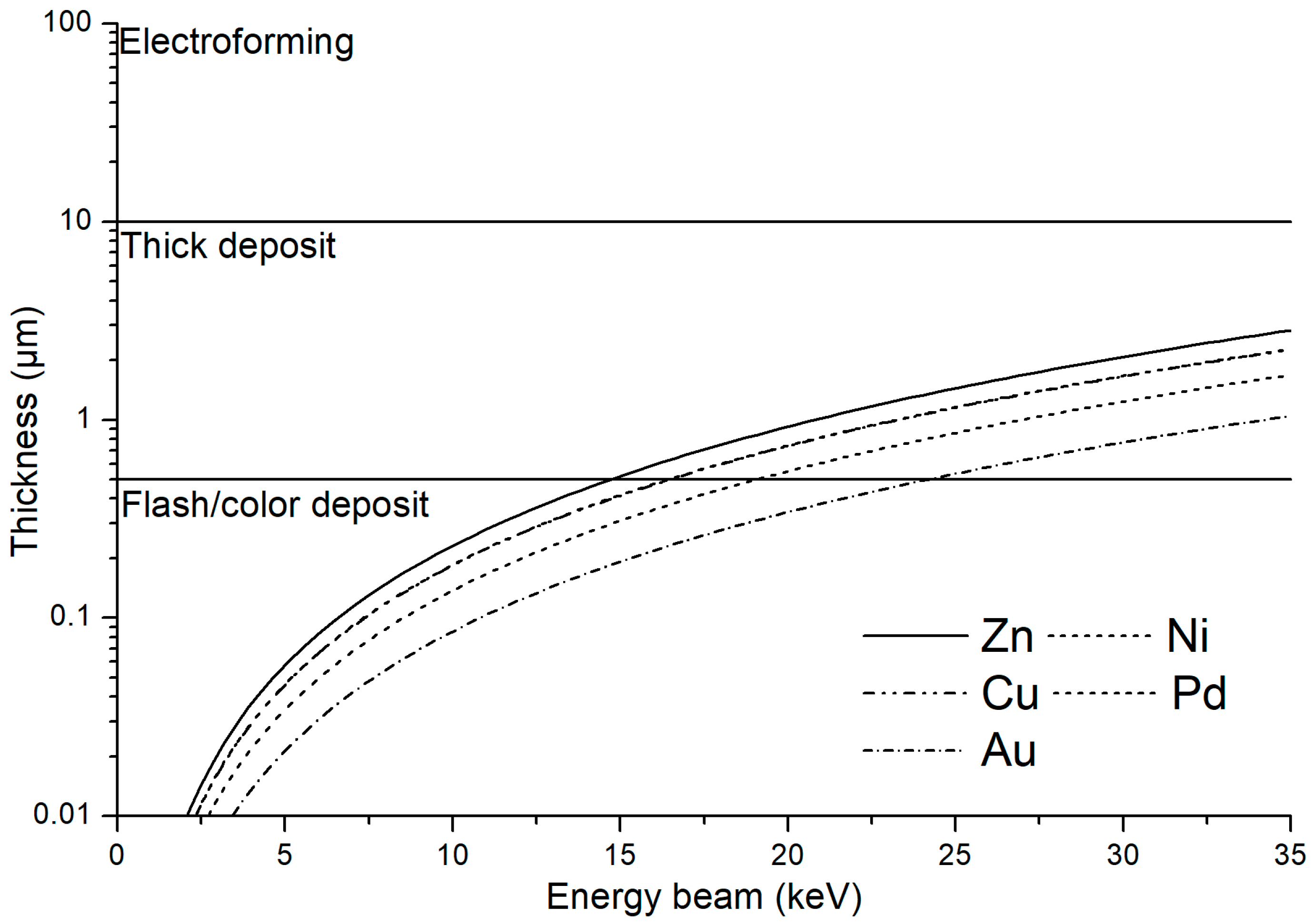
2. Materials and Methods
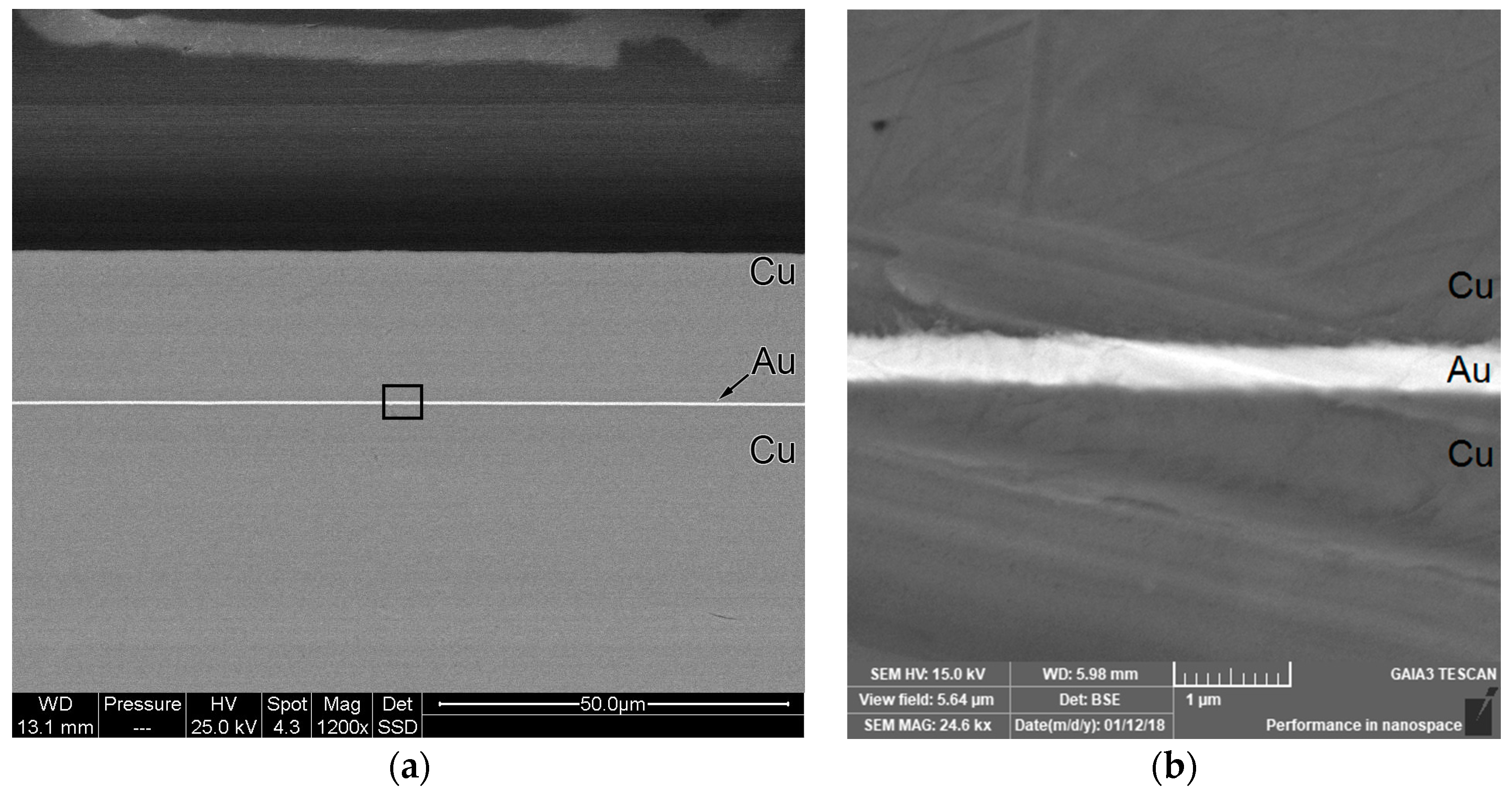
2.1. Samples Preparation
2.2. EDX Measurements
2.3. Simulations of the Standards
- 80, 110, 150, 200, 270, 340, 390, 450, 520, 600, 700 nm of Au on Cu
- 110, 140, 190, 260, 370, 500, 570, 660, 760, 890, 1090 nm of Pd on Cu
- 45, 60, 80, 110, 150, 200, 250, 300, 350, 400, 460, 540 nm of Ni on Cu
- Au, Pd, Ni, Cu bulk pure elements
2.4. Quantification
2.5. Fitting
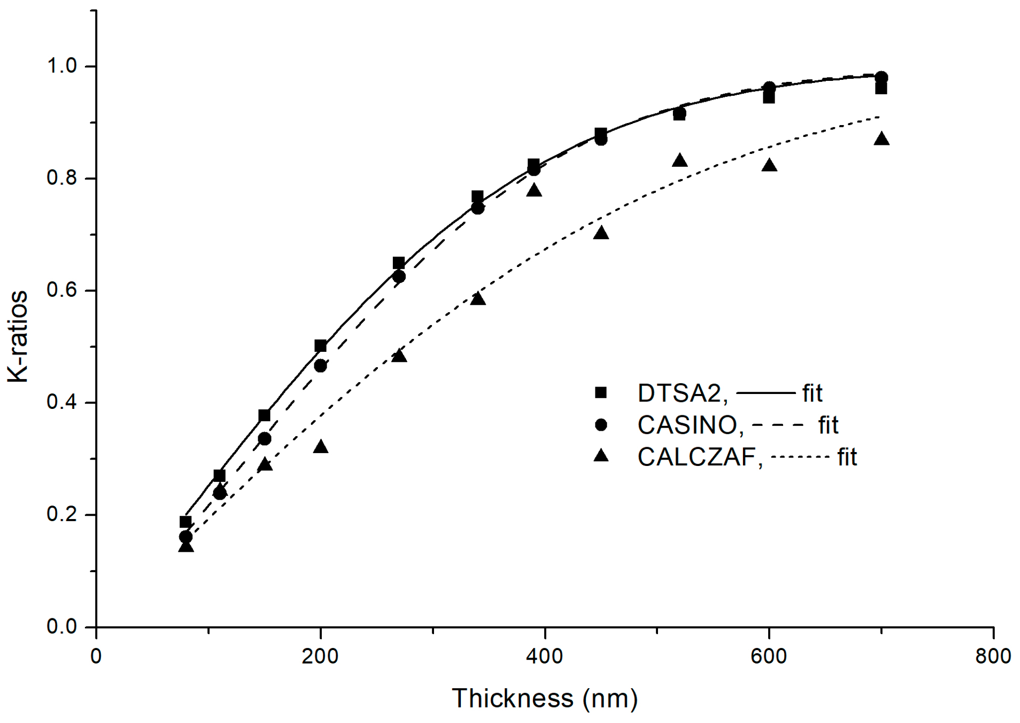
3. Results
3.1. Sputtering Samples Thickness
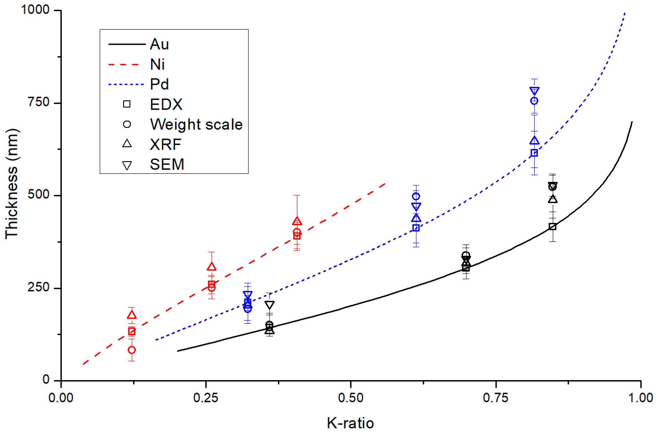
3.2. Galvanic Samples Thickness and Composition
4. Conclusions
Acknowledgments
Author Contributions
Conflicts of Interest
References
- Malarde, D.; Powell, M.J.; Quesada-Cabrera, R.; Wilson, R.L.; Carmalt, C.J.; Sankar, G.; Parkin, I.P.; Palgrave, R.G. Optimized Atmospheric-Pressure Chemical Vapor Deposition Thermochromic VO2 Thin Films for Intelligent Window Applications. ACS Omega 2017, 2, 1040–1046. [Google Scholar] [CrossRef]
- Nash, C.R.; Fenton, J.C.; Constantino, N.G.N.; Warburton, P.A. Compact chromium oxide thin film resistors for use in nanoscale quantum circuits. J. Appl. Phys. 2014, 116. [Google Scholar] [CrossRef]
- Bardi, U.; Caporali, S.; Chenakin, S.P.; Lavacchi, A.; Miorin, E.; Pagura, C.; Tolstogouzov, A. Characterization of electrodeposited metal coatings by secondary ion mass spectrometry. Surf. Coat. Technol. 2006, 200, 2870–2874. [Google Scholar] [CrossRef]
- Bardi, U.; Chenakin, S.P.; Ghezzi, F.; Giolli, C.; Goruppa, A.; Lavacchi, A.; Miorin, E.; Pagura, C.; Tolstogouzov, A. High-temperature oxidation of CrN/AlN multilayer coatings. Appl. Surf. Sci. 2005, 252, 1339–1349. [Google Scholar] [CrossRef]
- Ortel, E.; Hertwig, A.; Berger, D.; Esposito, P.; Rossi, A.M.; Kraehnert, R.; Hodoroaba, V.-D. New Approach on Quantification of Porosity of Thin Films via Electron-Excited X-ray Spectra. Anal. Chem. 2016, 88, 7083–7097. [Google Scholar] [CrossRef] [PubMed]
- Richter, S.; Pinard, P.T. Combined EPMA, FIB and Monte Carlo simulation: A versatile tool for quantitative analysis of multilayered structures. IOP Conf. Ser. Mater. Sci. Eng. 2016, 109, 12014. [Google Scholar] [CrossRef]
- Eggert, F. EDX-spectra simulation in electron probe microanalysis. Optimization of excitation conditions and detection limits. Microchim. Acta 2006, 155, 129–136. [Google Scholar] [CrossRef]
- Armigliato, A. Thin film X-ray microanalysis with the analytical electron microscope. J. Anal. At. Spectrom. 1999, 14, 413–418. [Google Scholar] [CrossRef]
- Christien, F.; Pierson, J.F.; Hassini, A.; Capon, F.; Le Gall, R.; Brousse, T. EPMA-EDS surface measurements of interdiffusion coefficients between miscible metals in thin films. Appl. Surf. Sci. 2010, 256, 1855–1890. [Google Scholar] [CrossRef]
- Pascual, R.; Cruz, L.R.; Ferreira, C.L.; Gomes, D.T. Thin film thickness measurement using the energy-dispersive spectroscopy technique in a scanning electron microscope. Thin Solid Films 1990, 185, 279–286. [Google Scholar] [CrossRef]
- Waldo, R.A.; Militello, M.C.; Gaarenstroom, S.W. Quantitative thin-film analysis with an energy-dispersive X-ray detector. Surf. Interface Anal. 1993, 20, 111–114. [Google Scholar] [CrossRef]
- Gauvin, R. Quantitative X-ray microanalysis of heterogeneous materials using Monte Carlo simulations. Microchim. Acta 2006, 155, 75–81. [Google Scholar] [CrossRef]
- Sokolov, S.A.; Kelm, E.A.; Milovanov, R.A.; Abdullaev, D.A.; Sidorov, L.N. Non-destructive determination of thickness of the dielectric layers using EDX. Proc. SPIE Int. Soc. Opt. Eng. 2016, 10224. [Google Scholar] [CrossRef]
- Stenberg, G.; Boman, M. Thickness measurement of light elemental films. Diam. Relat. Mater. 1996, 5, 1444–1449. [Google Scholar] [CrossRef]
- Willich, P.; Obertop, D. Composition and thickness of submicron metal coatings and multilayers on Si determined by EPMA. Surf. Interface Anal. 1988, 13, 20–24. [Google Scholar] [CrossRef]
- Hunger, H.-J.; Baumann, W.; Schulze, S. A new method for determining the thickness and composition of thin layers by electron probe microanalysis. Cryst. Res. Technol. 1985, 20, 1427–1433. [Google Scholar] [CrossRef]
- Ares, J.R.; Pascual, A.; Ferrer, I.J.; Sánchez, C. A methodology to reduce error sources in the determination of thin film chemical composition by EDAX. Thin Solid Films 2004, 450, 207–210. [Google Scholar] [CrossRef]
- Sempf, K.; Herrmann, M.; Bauer, F. First results in thin film analysis based on a new EDS software to determine composition and/or thickness of thin layers on substrates. In Proceedings of the EMC 2008 14th European Microscopy Congress, Aachen, Germany, 1–5 September 2008; Springer: Aacher, Germany, 2008; pp. 751–752. [Google Scholar]
- Hodoroaba, V.-D.; Kim, K.J.; Unger, W.E.S. Energy dispersive electron probe microanalysis (ED-EPMA) of elemental composition and thickness of Fe-Ni alloy films. Surf. Interface Anal. 2012, 44, 1459–1461. [Google Scholar] [CrossRef]
- Raymond Casting Application of Electron Probes to Local Chemical and Crystallographic Analysis. 1951. Available online: http://www.microbeamanalysis.org/history/Castaing-Thesis-clearscan.pdf (accessed on 14 February 2018).
- Ritchie, N.W.M. Efficient Simulation of Secondary Fluorescence via NIST DTSA-II Monte Carlo. Microsc. Microanal. 2017, 23, 618–633. [Google Scholar] [CrossRef] [PubMed]
- Kühn, J.; Hodoroaba, V.-D.; Linke, S.; Moritz, W.; Unger, W.E.S. Characterization of Pd-Ni-Co alloy thin films by ED-EPMA with application of the STRATAGEM software. Surf. Interface Anal. 2012, 44, 1456–1458. [Google Scholar] [CrossRef]
- Ritchie, N.W.M. Spectrum simulation in DTSA-II. Microsc. Microanal. 2009, 15, 454–468. [Google Scholar] [CrossRef] [PubMed]
- Osada, Y. Electron probe microanalysis (EPMA) measurement of aluminum oxide film thickness in the nanometer range on aluminum sheets. X-ray Spectrom. 2005, 34, 92–95. [Google Scholar] [CrossRef]
- Bastin, G.F.; Heijligers, H.J.M. A systematic database of thin-film measurements by EPMA: Part I—Aluminum films. X-ray Spectrom. 2000, 29, 212–238. [Google Scholar] [CrossRef]
- Merlet, C. Thin film quantification by EPMA: Accuracy of analytical procedure. Microsc. Microanal. 2006, 12, 842. [Google Scholar] [CrossRef]
- August, H.; Wernisch, J. A Method for Determining the Mass Thickness of Thin Films Using Electron Probe Microanalysis. Scanning 1987, 9, 145–155. [Google Scholar] [CrossRef]
- Shang, Y.; Guo, Y.; Liu, Z.; Xu, L. An EPMA software for determination of thin metal film thickness and it’s application. Acta Metall. Sin. 1997, 33, 443–448. [Google Scholar]
- Watanabe, M.; Horita, Z.; Nemoto, M. Absorption correction and thickness determination using the zeta factor in quantitative X-ray microanalysis. Ultramicroscopy 1996, 65, 187–198. [Google Scholar] [CrossRef]
- Bishop, H.E.; Poole, D.M. A simple method of thin film analysis in the electron probe microanalyser. J. Phys. D Appl. Phys. 1973, 6, 1142–1158. [Google Scholar] [CrossRef]
- Canli, S. Thickness Analysis of Thin Films by Energy Dispersive X-ray Spectroscopy. 2010. Available online: https://etd.lib.metu.edu.tr/upload/12612822/index.pdf (accessed on 14 February 2018).
- Bastin, G.F.; Dijkstra, J.M.; Heijligers, H.J.M.; Klepper, D. In-depth profilingwith the electron probe microanalyser. In Proceedings of the EMAS’98 3rd Regional Workshop, Barcelona, Spain, 3–16 May 1998; pp. 25–55. [Google Scholar]
- Roming, A.D.; Plimpton, S.J.; Michael, J.R.; Myklebust, R.L. Newbury DE Microbeam Analysis; San Francisco Press: San Francisco, CA, USA, 1990. [Google Scholar]
- Kyser, D.F.; Murata, K. Quantitative Electron Microprobe Analysis of Thin Films on Substrates. IBM J. Res. Dev. 1974, 352–363. [Google Scholar] [CrossRef]
- Moller, A.; Weinbruch, S.; Stadermann, F.J.; Ortner, H.M.; Neubeck, K.; Balogh, A.G.; Hahn, H. Accuracy of film thickness determination in electron-probe microanalysis. Mikrochim. Acta 1995, 119, 41–47. [Google Scholar] [CrossRef]
- Procop, M.; Radtke, M.; Krumrey, M.; Hasche, K.; Schädlich, S.; Frank, W. Electron probe microanalysis (EPMA) measurement of thin-film thickness in the nanometre range. Anal. Bioanal. Chem. 2002, 374, 631–634. [Google Scholar] [CrossRef] [PubMed]
- Campos, C.S.; Coleoni, E.A.; Trincavelli, J.C.; Kaschny, J.; Hubbler, R.; Soares, M.R.F.; Vasconcellos, M.A.Z. Metallic thin film thickness determination using electron probe microanalysis. X-ray Spectrom. 2001, 30, 253–259. [Google Scholar] [CrossRef]
- Zhuang, L.; Bao, S.; Wang, R.; Li, S.; Ma, L.; Lv, D. Thin film thickness measurement using electron probe microanalyzer. In Proceedings of the International Conference on Applied Superconductivity and Electromagnetic Devices (ASEMD 2009), Chengdu, China, 25–27 September 2009; pp. 142–144. [Google Scholar] [CrossRef]
- Ng, F.L.; Wei, J.; Lai, F.K.; Goh, K.L. Thickness Measurement of Metallic Thin Film by X-ray Microanalysis; SIMTech Technical Reports; Singapore Institute of Manufacturing Technology: Singapore, 2010; Volume 11, pp. 21–25. [Google Scholar]
- Dumelié, N.; Benhayoune, H.; Balossier, G. TF_Quantif: A Quantification Procedure for Electron Probe Microanalysis of Thin Films on Heterogeneous Substrates. J. Phys. D 2007, 40, 2124. [Google Scholar] [CrossRef]
- Pouchou, J.L.; Pichoir, F. Surface film X-ray microanalysis. Scanning 1990, 12, 212–224. [Google Scholar] [CrossRef]
- Instruments, O. LayerProbe. Available online: https://www.oxford-instruments.com/products/microanalysis/solutions/layerprobe (accessed on 14 February 2018).
- Instruments, O. ThinFilmID. Available online: http://www.oxford-instruments.cn/OxfordInstruments/media/nanoanalysis/brochures and thumbs/ThinFilmID_Brochure.pdf (accessed on 14 February 2018).
- Katz, L.; Penfold, A.S. Range-energy relations for electrons and the determination of beta-ray end-point energies by absorption. Rev. Mod. Phys. 1952, 24, 28–44. [Google Scholar] [CrossRef]
- Cockett, G.H.; Davis, C.D. Coating thickness measurement by electron probe microanalysis. Br. J. Appl. Phys. 1963, 14, 813–816. [Google Scholar] [CrossRef]
- EDAX Genesis. Available online: http://www.edax.com/support/software-licensing (accessed on 14 February 2018).
- Pathfinder. Available online: https://www.thermofisher.com/order/catalog/product/IQLAADGABKFAQOMBJE (accessed on 14 February 2018).
- ImageJ. Available online: https://imagej.nih.gov/ij/ (accessed on 14 February 2018).
- DTSA-II. Available online: http://www.cstl.nist.gov/div837/837.02/epq/dtsa2/ (accessed on 14 February 2018).
- CASINO. Available online: http://www.gel.usherbrooke.ca/casino/ (accessed on 14 February 2018).
- Demers, H.; Poirier-Demers, N.; Couture, A.R.; Joly, D.; Guilmain, M.; De Jonge, N.; Drouin, D. Three-dimensional electron microscopy simulation with the CASINO Monte Carlo software. Scanning 2011, 33, 135–146. [Google Scholar] [CrossRef] [PubMed]
- CalcZAF. Available online: http://www.probesoftware.com/Technical.html (accessed on 14 February 2018).


| Extrapolation Method | EDX–XRF Deviation |
|---|---|
| BICS/DTSA2 | 9.6% |
| BICS/CASINO | 9.7% |
| BICS/CALCZAF | 20.4% |
| DTSA2/DTSA2 | 24.8% |
| DTSA2/CASINO | 27.0% |
| DTSA2/CALCZAF | 50.1% |
| Sample | Weight Scale (nm) | XRF (nm) | SEM Cross Section (nm) | EDX (nm) | EDX-XRF Deviation |
|---|---|---|---|---|---|
| Au1 | 151 ± 31 | 135 ± 8 | 207 ± 30 | 143 ± 14 | 5% |
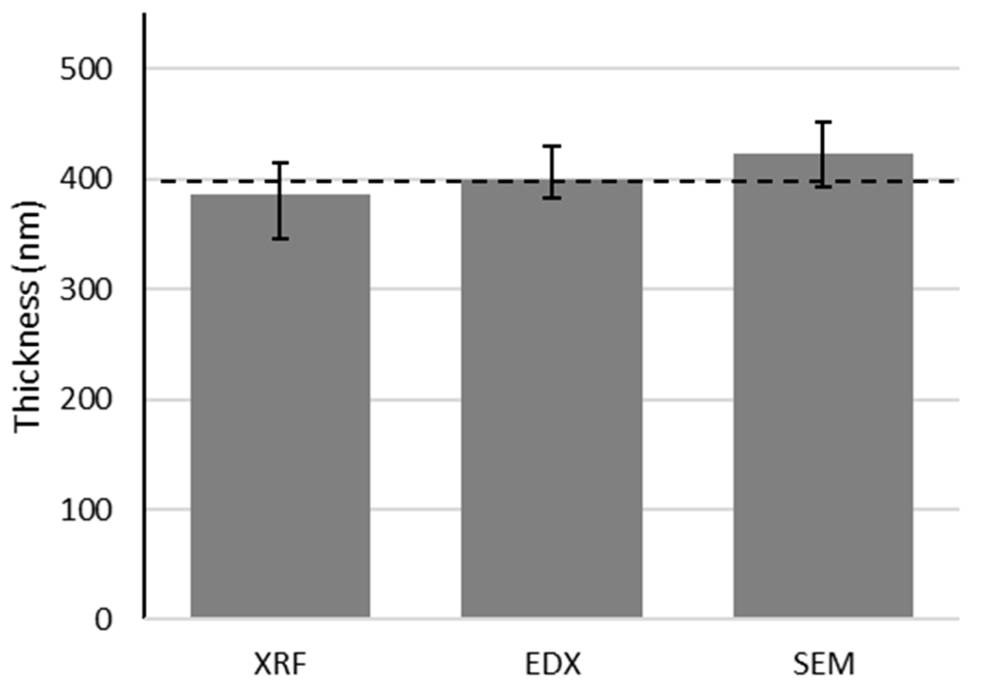
| Au2 | 338 ± 30 | 318 ± 29 | 329 ± 30 | 304 ± 29 | −5% |
| Au3 | 523 ± 32 | 488 ± 49 | 528 ± 30 | 416 ± 40 | −15% |
| Pd4 | 193 ± 30 | 204 ± 50 | 234 ± 30 | 210 ± 20 | 3% |
| Pd5 | 498 ± 30 | 437 ± 76 | 473 ± 30 | 412 ± 40 | −6% |
| Pd6 | 755 ± 32 | 647 ± 71 | 785 ± 30 | 615 ± 59 | −5% |
| Ni7 | 83 ± 30 | 176 ± 22 | n.a. | 133 ± 13 | −24% |
| Ni8 | 251 ± 30 | 306 ± 42 | n.a. | 260 ± 25 | −15% |
| Ni9 | 401 ± 32 | 429 ± 72 | n.a. | 390 ± 38 | −9% |
| Thickness (nm) | Energy Beam (keV) | Ni (wt.%) | Cu (wt.%) | Au (wt.%) | Ni:Au % |
|---|---|---|---|---|---|
| 200 | 20 | 1.79 | 20.60 | 77.61 | 2.25 |
| 400 | 20 | 2.28 | 9.89 | 87.83 | 2.53 |
| 600 | 20 | 2.28 | 7.94 | 89.79 | 2.48 |
| Bulk | 20 | 2.60 | 0.00 | 97.40 | 2.60 |
| 400 | 15 | 2.16 | 7.61 | 90.24 | 2.34 |
| 400 | 25 | 1.90 | 11.93 | 86.17 | 2.16 |
| Sample | 15 | 1.88 | 4.61 | 93.50 | 1.97 |
| Sample | 20 | 2.69 | 8.08 | 89.23 | 2.92 |
| Sample | 25 | 2.15 | 14.42 | 83.43 | 2.52 |
© 2018 by the authors. Licensee MDPI, Basel, Switzerland. This article is an open access article distributed under the terms and conditions of the Creative Commons Attribution (CC BY) license (http://creativecommons.org/licenses/by/4.0/).
Share and Cite
Giurlani, W.; Innocenti, M.; Lavacchi, A. X-ray Microanalysis of Precious Metal Thin Films: Thickness and Composition Determination. Coatings 2018, 8, 84. https://doi.org/10.3390/coatings8020084
Giurlani W, Innocenti M, Lavacchi A. X-ray Microanalysis of Precious Metal Thin Films: Thickness and Composition Determination. Coatings. 2018; 8(2):84. https://doi.org/10.3390/coatings8020084
Chicago/Turabian StyleGiurlani, Walter, Massimo Innocenti, and Alessandro Lavacchi. 2018. "X-ray Microanalysis of Precious Metal Thin Films: Thickness and Composition Determination" Coatings 8, no. 2: 84. https://doi.org/10.3390/coatings8020084
APA StyleGiurlani, W., Innocenti, M., & Lavacchi, A. (2018). X-ray Microanalysis of Precious Metal Thin Films: Thickness and Composition Determination. Coatings, 8(2), 84. https://doi.org/10.3390/coatings8020084