Article

Growth of NbC Thin Film Using CH4 as a Carbon Source and Reducing Agent

1
School of Advanced Materials Science and Engineering, Sungkyunkwan University, Suwon 16419, Korea
2
SKKU Advanced Institute of Nanotechnology, Sungkyunkwan University, Suwon 16419, Korea
3
Department of Materials Science and Engineering, Ajou University, Suwon 16499, Korea
4
Department of Energy Systems Research, Ajou University, Suwon 16499, Korea
*
Author to whom correspondence should be addressed.
These authors contributed equally to this study.
Coatings 2018, 8(11), 379; https://doi.org/10.3390/coatings8110379
Submission received: 16 August 2018 / Revised: 17 October 2018 / Accepted: 23 October 2018 / Published: 24 October 2018
(This article belongs to the Special Issue Design and Synthesis of Hard Coatings)

Abstract

:
Transition metal carbides (TMCs) have high melting points, hardness, and chemical stabilities in acidic media. In this work, a chemical vapor deposition method using CH4 as a carbon source and reducing agent was employed to make an NbC film. NbCl5 carried by Ar gas was used as an Nb precursor. An NbC thin film, deposited on a c-plane sapphire, exhibited a preferential orientation of the (111) plane, which can be explained by domain-matching epitaxy. A nanoindentation test showed that the NbC film with the preferential orientation of the (111) plane was stronger than that with a random orientation. Moreover, the results showed that H2, which is conventionally used as a reducing agent in NbC synthesis, degraded the crystallinity and hardness of the fabricated NbC.

1. Introduction

Transition metal carbides (TMCs) have attracted significant attention as materials with high melting points, hardness, chemical stabilities in acidic media, and thermal stabilities [1,2,3,4,5]. Owing to these unique properties, they have been used in various applications such as cutting tools [6,7], wear-resistant materials [8], and hard electrical contacts [9]. Recently, TMCs are being increasingly utilized as supporting materials for various electrocatalyst materials [10,11] or as electrocatalyst materials themselves [12,13]. Among the various carbide materials, niobium carbide (NbC) has excellent abovementioned properties (highest melting point: 3610 °C, high Young’s modulus: 380–480 GPa) and superconducting properties (below 12 K), which make it promising for various applications such as a reinforced phase in an iron matrix, hard coating, and wear protection [14,15,16,17]. Furthermore, NbC is potentially applicable as an electrical contact coating material owing to its low electrical resistivity (3.5 × 10⁻⁵ Ω∙cm) [18] and excellent wear-resistance [19], replacing the noble metal with a low wear resistivity and high cost.
Conventionally, the synthesis of an NbC thin film is performed by the direct reaction between Nb metal and carbon owing to the very high melting point [20,21]. However, as the melting point of Nb reaches 2744 °C, a chemical compound containing Nb such as NbCl5 (melting point: 205 °C) was used as a precursor [22,23]. Nb flux can be obtained by heat treatment of NbOx in a reducing atmosphere (hydrogen gas or additives such as NaF); however, this reaction has a disadvantage as a high temperature of 1000 °C (or larger) is required [24,25,26].
In this study, we aimed to synthesize NbC thin films using methane (CH4) gas as a source that provides carbon as well as a reducing atmosphere. NbCl5 was used as a precursor of Nb. An analysis of the crystal structure for each flow rate of CH4 was performed to optimize the production of high-quality NbC films without the formation of oxides. In addition, the mechanical, electrical, and thermal properties of NbC can vary owing to the difference in the atomic arrangement depending on the crystal orientation of the NbC thin film (conventionally, the rock-salt NbC crystal structure has anisotropic properties between (111) and (100) planes). Therefore, we studied the preferential orientation of NbC depending on the type of substrate, and changes in physical properties depending on structural differences in terms of crystallinity (single-crystal or polycrystal) and crystal orientation.

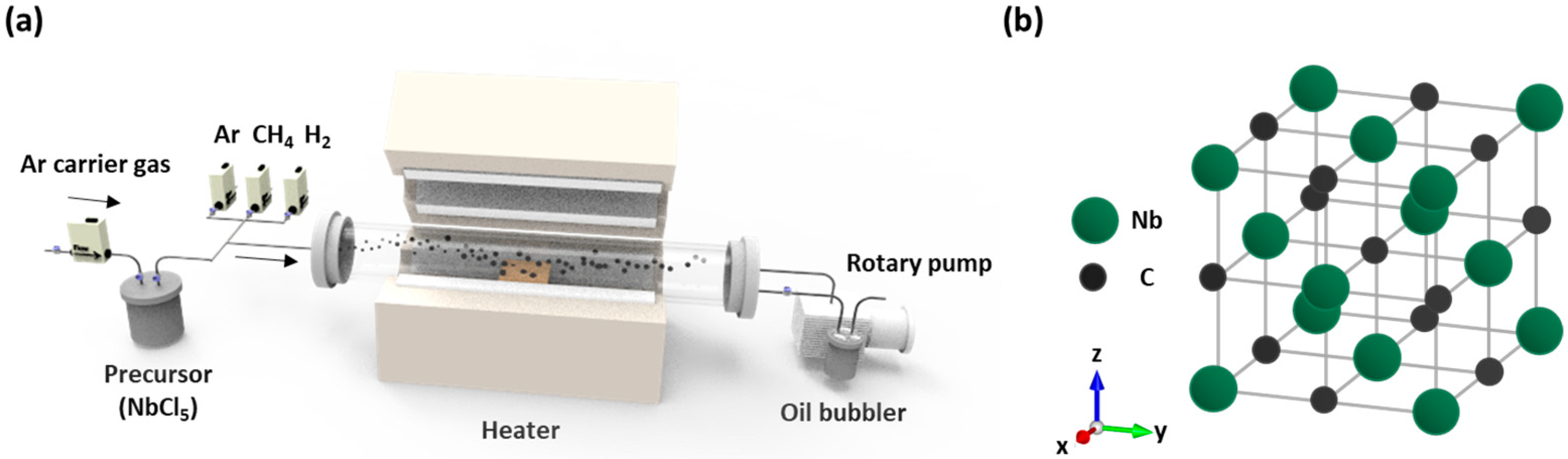
2. Materials and Methods

2.1. Preparation of Coatings

Growths of NbC were performed on a single-crystal c-plane sapphire substrate (Namkang Hi-tech Co., Ltd., SaR 100-500, Gyeonggi-do, Korea) and single-crystal Si (100) substrate using a quartz-tube furnace. Single-crystal Si (100) substrates were prepared by dipping a silicon thermal oxide wafer in an HF:H2O solution with a volume ratio of 1:1 for 1 min. A schematic of the reaction system is shown in Figure 1a. NbCl5 (Alfa Aesar, #11548, Ward Hill, MA, USA), used as an Nb precursor, was placed in a stainless-steel canister, which was heated by a heating mantle. The sublimed NbCl5 and Ar carrier gas were introduced into the tube through a ¼-inch stainless-steel gas line, which was wrapped and heated by a commercial heating tape. The temperatures of the canister and line were maintained at 140 and 160 °C, respectively. The substrates were loaded into the tube furnace and the system was pumped down to vacuum and refilled with Ar gas to obtain atmospheric pressure. The furnace temperature was increased to 900 °C within 40 min in an Ar–CH4 or Ar–CH4–H2 environment. The gas flow rates of Ar and H2 were 200 sccm, while that of CH4 was in the range of 5 to 200 sccm. After the temperature reached 900 °C, the growth of NbC was initiated by introducing another flow (200 sccm) of Ar carrier gas through the canister to the furnace. After the growth for 30 min, the Nb-precursor supply line was closed, and the samples were rapidly cooled under the Ar environment.

2.2. Structure and Property Characterization

An X-ray diffractometer (XRD) (Bruker D8-Advance with monochromated Cu-Kα1 radiation; scan rate of 0.05°/s, Billerica, MA, USA) was used for identification of the samples. The surface morphologies of the samples were investigated by scanning electron microscopy (SEM) (Hitachi, S-4800, Tokyo, Japan). Transmission electron microscopy (TEM) (JEOL, JEM-2100F, at 200 kV, Tokyo, Japan) was employed to analyze the structures of the samples. The TEM sample was prepared by scraping off the NbC onto the TEM grid. A pole figure analysis was conducted to study the symmetry of the sample using an X-ray diffractometer (PANalytical, X’pert PRO using Cu-Kα radiation, Westborough, MA, USA, χ: 0°–75° and φ: 0°–360° at 2θ of 40.32°). The mechanical properties of the NbC samples were characterized by a nanoindentation tester (Anton Parr, Graz, Austria, ultra-precision surface mechanical analyzer). The nanoindentation tests have been performed using a Berkovich diamond indenter. The as-received radius of the tip was 50 nm, and the tip was calibrated on a fused silica reference sample. The hardness and elastic modulus of samples were obtained by averaging the results of 5 indents. However, for the NbC film grown in the absence of H2 on a sapphire substrate, only a single indentation was performed due to damage that could be caused to the indenter because of the hardness of the sample.

3. Results and Discussion

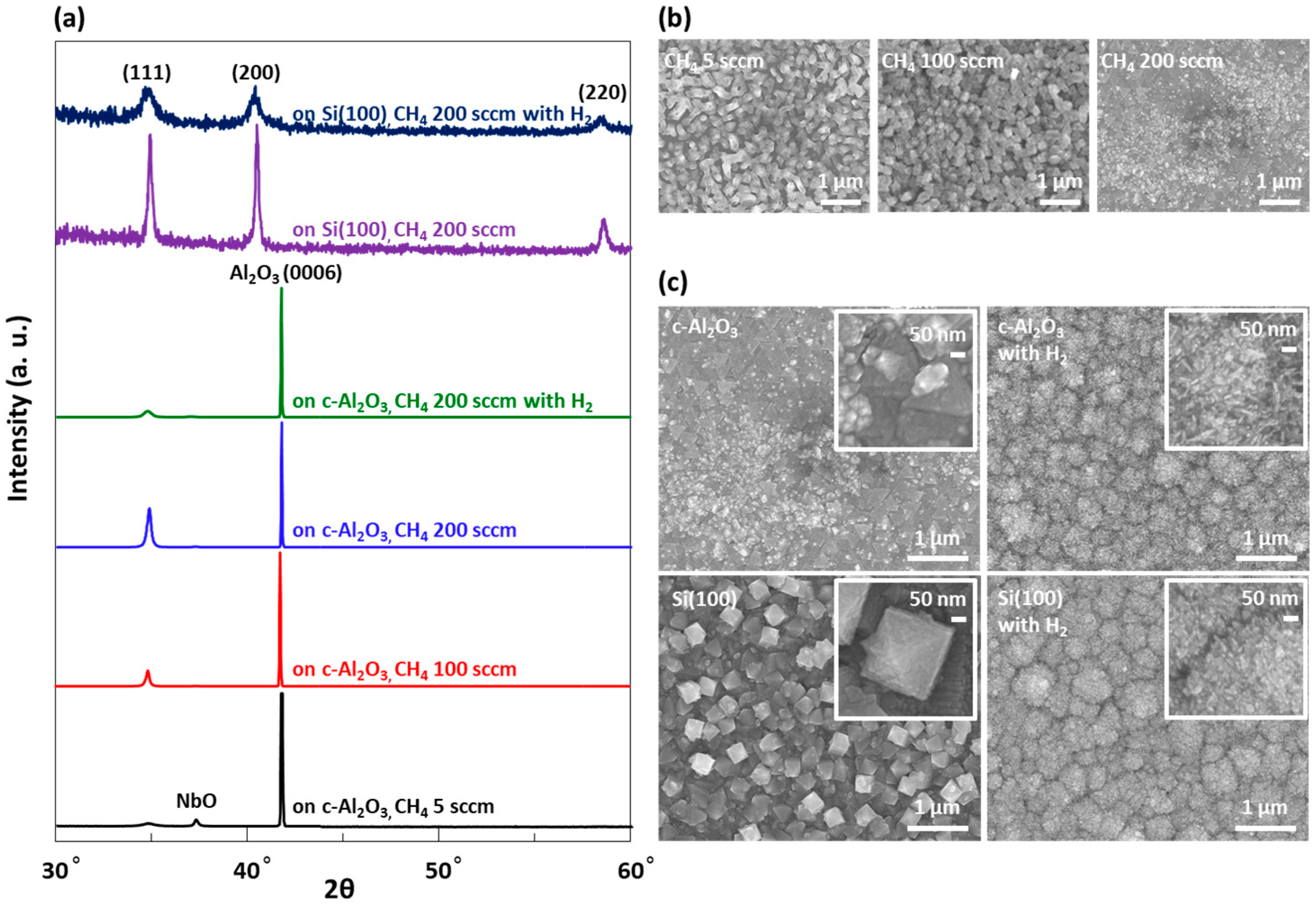
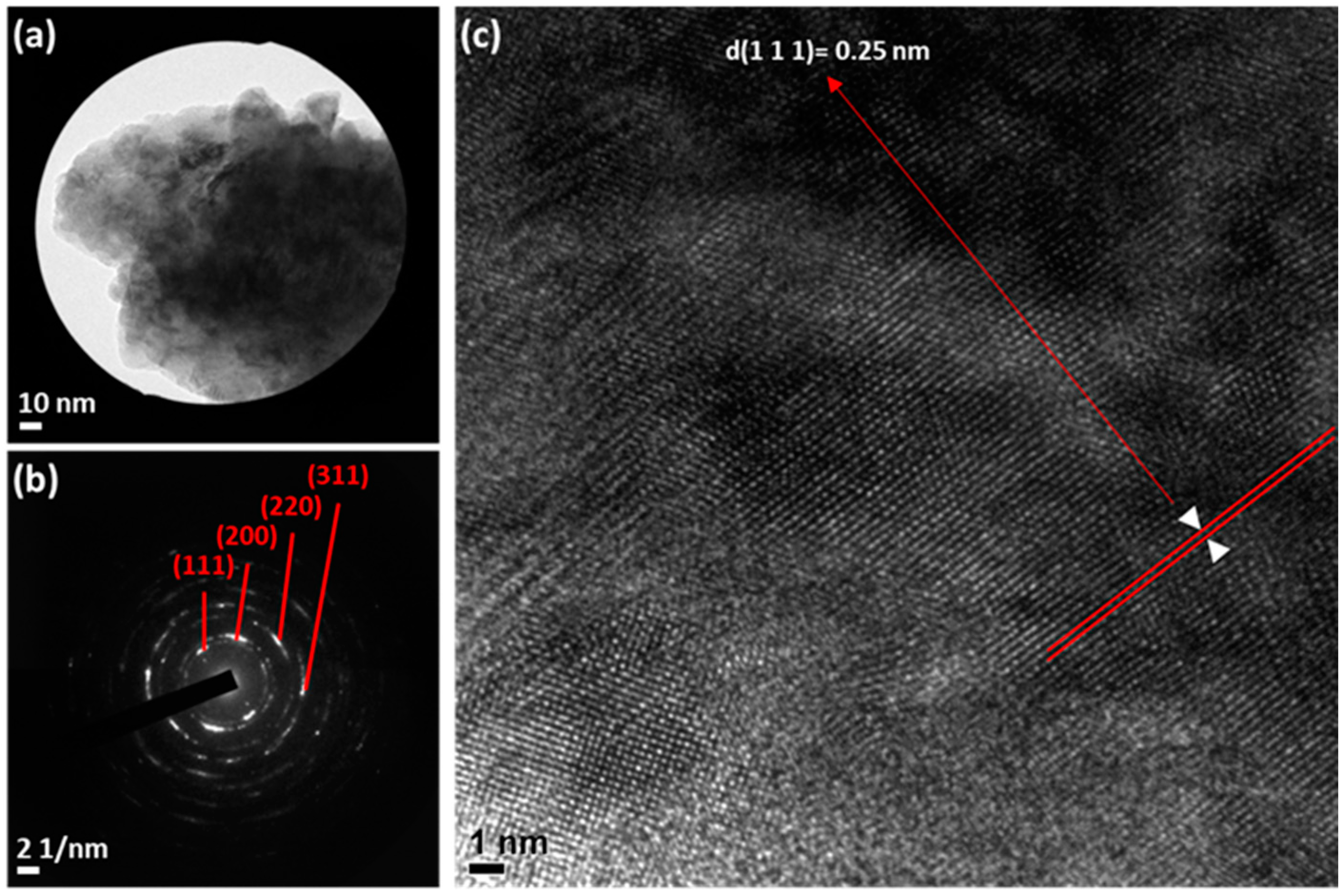
3.1. Morphology and Structural Characterization

NbC has a cubic crystal rock-salt structure (lattice constant = 4.47 Å), as shown in Figure 1b. In order to reveal the variations of the NbC growth depending on the flow rate of CH4, type of substrate, and presence of H2, we performed XRD and SEM analyses, see Figure 2. With the increase in the flow rate of CH4 from 5 to 100 sccm, the NbO peak (Joint Committee on Powder Diffraction Standards (JCPDS) No. 43-1290) decreases, while the intensity and sharpness of the peak at 2θ = 34.73° (JCPDS No. 38-1364) [27], corresponding to the NbC (111) plane, increase in the XRD patterns, see Figure 2a). The XRD patterns on a logarithmic scale are also presented in Figure S1. Nb oxide was formed by a reaction between oxygen remaining in the furnace and Nb precursor (ΔGf of NbO at 300 K is −391.77 kJ/mol, while that of NbC at 300 K is −136.878 kJ/mol); CH4 acts not only as a carbon source in the NbC formation but also as a reducing agent to reduce the oxide. The NbC (111) peak further increased with the increase in the CH4 flow rate to 200 sccm. The SEM images, as shown in Figure 2b, show that the density of NbC increases with the flow rate of CH4.
In addition, the NbC growth varied depending on the type of substrate. A comparison of NbC samples grown at the CH4 flow rate of 200 sccm on c-plane sapphire and Si (100) shows that the NbC film deposited on the c-plane sapphire exhibits only the (111) peak, while that on Si (100) exhibits (200) and (220) peaks in addition to the (111) peak in the XRD pattern. The peak intensity is higher for the NbC film grown on the c-plane sapphire. The NbC (111) peak intensity of the NbC film deposited on the c-plane sapphire is approximately 100 times higher than that of the film on Si (100). This indicates that the NbC film deposited on the c-plane sapphire has a preferential orientation of the (111) plane, whereas that on the Si (100) substrate is relatively randomly oriented and has a low crystallinity. The SEM images, see Figure 2c, show dense triangular domains of NbC on the c-plane sapphire and less-dense octahedral-shape NbC domains on Si (100).
We also analyzed changes in crystallinity of NbC in the presence of H2. The XRD patterns show that the addition of H2 flow (200 sccm) under the same CH4 flow rate weakens the intensity and sharpness of the peaks on both c-plane sapphire and Si (100) substrates, which suggests that the presence of H2 decreases their crystallinity. This can be also observed in the SEM images, see Figure 2c. In the absence of H2, NbC grew in an angular shape, whereas in the presence of H2, the grown NbC had a rough surface. For quantitative comparison, we used the Scherrer equation on the NbC (111) peak and the calculated crystallite size of each film was as follows: 37 nm (on c-plane sapphire, without H2), 40 nm (on Si, without H2), 20 nm (on c-plane sapphire, with H2) [28]. The above results may be related to the property of NbC that enables it to capture hydrogen. For example, NbC precipitates added to alloys such as steel act as hydrogen traps to interfere with hydrogen diffusion, thereby improving the resistance to hydrogen-induced cracking (HIC) of steel [29,30]. The swollen shape of the films grown with H2 shows the possibility for this phenomenon.
Figure 3 shows TEM images (Figure 3a,c) of the NbC film grown on sapphire without H2 and its corresponding selected-area electron diffraction (SAED) pattern, see Figure 3b, obtained from the area in Figure 3a. In the SAED pattern, the distances from the center to each ring are 3.982 1/nm (0.251 nm), 4.572 1/nm (0.219 nm), 6.499 1/nm (0.154 nm), and 7.68 1/nm (0.130 nm), and these correspond to the (111), (200), (220), and (311) lattice planes of NbC, respectively. The ring-shaped patterns in the SAED pattern indicate that the sample is polycrystalline and that it has no symmetry. It is considered that this is the result of overlapping NbC particles during the preparation of the TEM sample because the NbC grown on c-plane sapphire has a (111) preferred orientation along the out-of-plane direction and has a six-fold symmetry in the in-plane direction (the in-plane analysis of the sample will be discussed in detail in the section below). The high-resolution TEM image, shown in Figure 3c, shows grains with different orientations and grain boundaries.

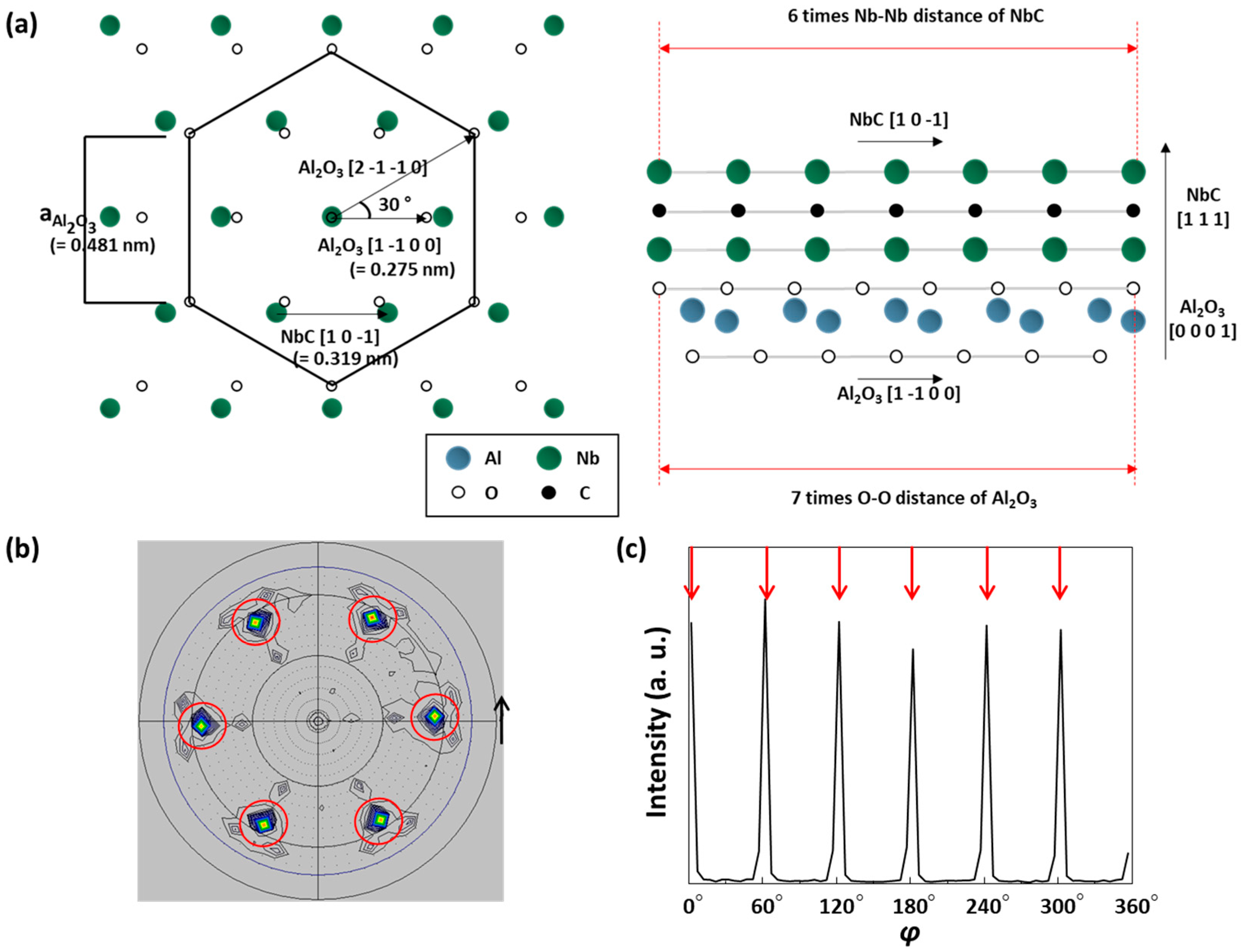
3.2. Epitaxial Growth Mechanism

The correlation between the (0001) plane of sapphire (Al2O3) and (111) plane of NbC was investigated to explain the observation that NbC on c-plane sapphire grows preferentially with the (111) plane. The coincident site lattice (CSL) [31,32,33,34] or domain-matching epitaxy (DME) theory [35,36,37,38] shows that the NbC (111) plane could grow epitaxially on the Al2O3 (0001) plane. Figure 4a shows schematic diagrams of this epitaxial relationship. The in-plane lattice mismatch between Al2O3 (0001) and NbC (111) is: f = (aAlOaNbC(111))/aAlO = (0.481 nm − 0.319 nm)/(0.481 nm) = 0.34, which is a very large value; therefore, an epitaxial growth is unlikely. However, the O–O interatomic distance along the [1-100] direction, at 30° from the [2-1-10] direction, is 0.275 nm. When the [1-100] direction on the (0001) plane of Al2O3 and [10-1] direction on the NbC (111) plane are arranged to be parallel, as shown in the top-view schematic diagram in Figure 4a, the f value is reduced to 0.16; therefore, an epitaxial growth can be expected. In this direction, as shown in the side-view schematic in Figure 4a, seven times the O–O distance of Al2O3 (0.275 nm × 7 = 1.925 nm) is almost equal to six times the Nb–Nb distance of NbC (0.319 nm × 6 = 1.914 nm).
Through this epitaxial relationship, the NbC is expected to have a six-fold symmetry on c-plane sapphire, and we performed the X-ray pole figure analysis to show this. When the pole figure was measured at a 2θ angle of 40.32°, the six-fold symmetry of NbC was confirmed as shown in Figure 4b,c. The 2θ angle of 40.32° is the angle for the (200) plane of NbC, and we can see that diffraction occurs, having 60° intervals when the chi (χ) angle is tilted by about 55°. This is because the (200) plane of NbC has an interplanar angle of 54.74° with respect to the (111) plane of NbC. Therefore, it can be seen that the (111) plane of NbC has a six-fold symmetry in the in-plane direction as the diffraction appears at intervals of 60°. This result can also be derived from analysis of the (220) plane, which has an interplanar angle of 35.26° with respect to the (111) plane of NbC see Figure S2.

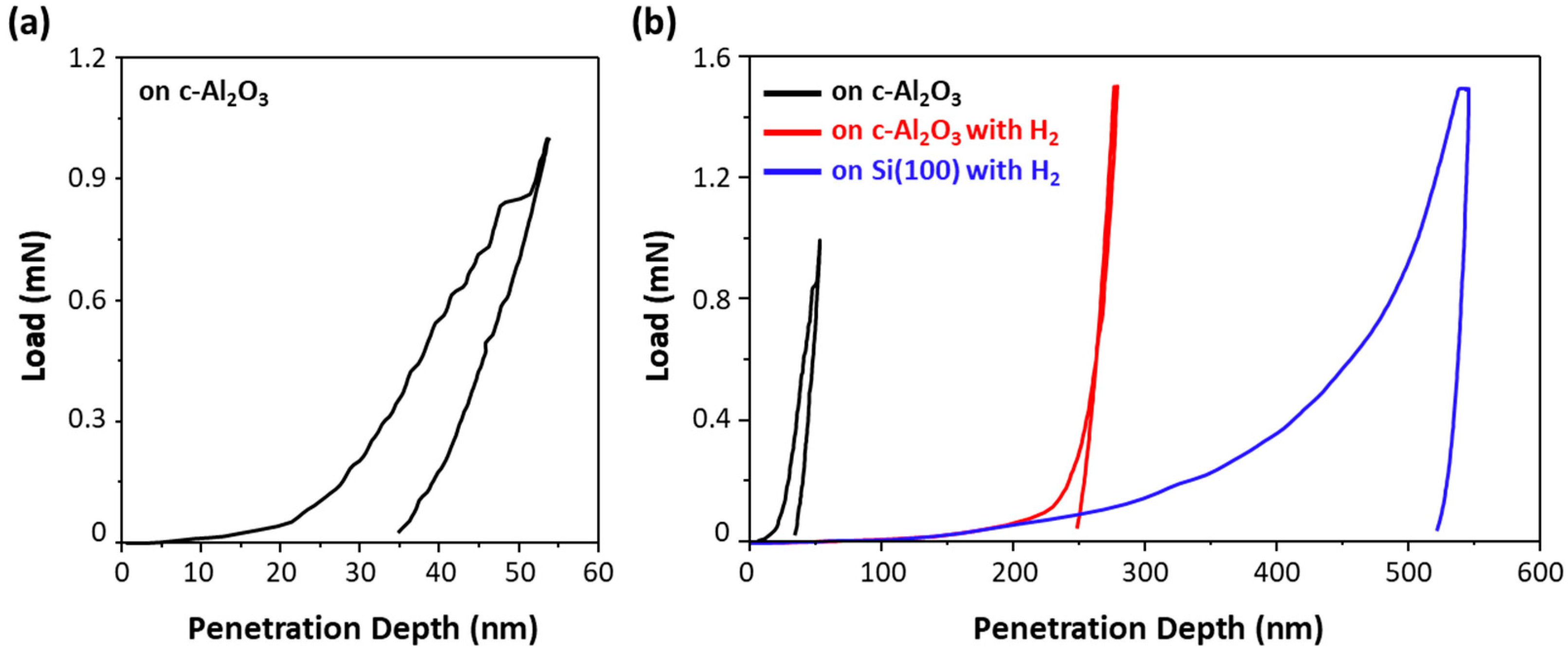
3.3. Mechanical Property Characterization

A nanoindentation test was performed to study the variations in the mechanical properties of the NbC films as a function of the crystal orientation and presence of H2 at the growth stage. Figure 5 shows load–displacement responses of the NbC films grown in the absence or presence of H2 on the c-plane sapphire, and that for the growth in the presence of H2 on Si (100). A measurement for NbC deposited without H2 on Si (100) was not possible owing to the surface morphology of the sample, as shown in Figure 2c. The penetration depth is measured by the difference in height between the indenter and reference tip. However, in the case of this sample, we could hardly adjust the zero point of the indenter with the reference tip. In Figure 5a, the penetration depth was only several tens of nanometers, which reveals that the NbC film grown in the absence of H2 on the c-plane sapphire is a very hard material. The hardness and elastic modulus of the sample were 10.94 GPa and 308.22 GPa, respectively. The values were automatically calculated with the Oliver–Pharr method [39,40]. At a penetration depth of approximately 45 nm, the parabolic curve is flattened, which can be regarded as a fracture due to the brittleness of the sample. When elastic modulus and hardness values are calculated with the Oliver–Pharr method in nanoindentation analysis, plastic depth (hp) is used [41,42]. Plastic depth is defined as the depth of the indenter in contact with the sample under load, and it can be obtained from the load-penetration depth curve. The x-intercept of the tangent line to the unloading curve at maximum load is the plastic depth. However, in our sample’s curve, the plastic depth value was obtained was larger than the actual value due to the increase of the penetration depth caused by the fracture as explained above. Therefore, it can be concluded that this affected the calculation of the values of elastic modulus and hardness of our sample. Since it was confirmed that the thickness of the film was about 300 nm with the cross-sectional SEM image, see Figure S3, the above data can be regarded as a result of the film not affected by the substrate (The thicknesses of the films grown with H2 are more than 1 µm). On the other hand, in the case of the NbC films grown in the presence of H2, initially, the slope is small, and the penetration depth is large. This is followed by a rapid increase in the slope, as shown in Figure 5b. The calculated hardness and elastic modulus of the film on c-plane sapphire with H2 were 0.75 and 54.52 GPa, and those values of the film on Si (100) with H2 were 0.21 and 50.51 GPa. We discussed above that H2 degraded the crystallinity of NbC and changed the surface morphology to a porous one, see Figure 2a,c and Figure S3. Therefore, it is considered that the surface of the material was softened owing to the degraded crystallinity and the changed surface morphology upon the introduction of H2. In addition, a comparison of the NbC films grown with H2 on the c-plane sapphire and Si (100) shows that the NbC film grown on the c-plane sapphire, which has the preferred orientation of the (111) plane, is stronger than the NbC film grown on Si (100), which has a random orientation and low crystallinity.

4. Conclusions

The NbC film grown on c-plane sapphire had a preferential orientation of the (111) plane, which could be explained by the CSL and DME theory. We deposited NbC using CH4 as a carbon source and confirmed that CH4 also acted as a reducing agent to remove the oxide formed by the reaction between oxygen remaining in the furnace and niobium precursor. On the Si (100) substrate, NbC grew without any preferential orientation and was softer than the NbC film grown on the c-plane sapphire with the preferential orientation of the (111) plane. Furthermore, we compared the differences in NbC growth between the samples obtained in the presence and absence of H2. The results showed that H2 at the growth stage lowered the crystallinity of NbC and led to a rough and soft surface.

Supplementary Materials

The following are available online at https://www.mdpi.com/2079-6412/8/11/379/s1, Figure S1: XRD patterns (logarithmic scale) of NbC films grown at different conditions; Figure S2: (a) X-ray pole figure of the NbC/c-sapphire system measured at a 2θ angle of 58.34° for the NbC (220) peak; (b) Azimuthal (φ) scan data measured at a χ angle of 35°; Figure S3: Cross-sectional SEM images of NbC films.

Author Contributions

Conceptualization, K.-W.K., B.J.K., H.K.Y., and J.-Y.C.; Methodology, K.-W.K., B.J.K., H.K.Y., and J.-Y.C.; Validation, K.-W.K., S.H.L., H.K.Y., and J.-Y.C.; Formal Analysis, K.-W.K., S.H.L., J.L., H.K.Y., and J.-Y.C.; Investigation, K.-W.K., S.H.L., H.K.Y., and I.J.C.; Resources, K.-W.K., S.H.L., H.K.L., and T.N.; Data Curation, K.-W.K., S.H.L., H.K.Y., and B.J.K.; Writing-Original Draft Preparation, K.-W.K.; Writing-Review and Editing, K.-W.K., H.K.Y., and J.-Y.C.; Visualization, B.J.K., B.J.J., and T.N.; Supervision, H.K.Y., and J.-Y.C.; Project Administration, B.J.K.; Funding Acquisition, J.-Y.C.

Funding

This research was supported by the Basic Science Research Program through the National Research Foundation of Korea (NRF), funded by the Ministry of Education, Science, and Technology [NRF-2018R1D1A1B07050253].

Acknowledgments

We gratefully thank Tae-Woo Lee of the Research Institute of Advanced Materials (RIAM) for the XRD and Pole figure measurement.

Conflicts of Interest

The authors declare no conflict of interest.

References

  1. Cuppari, M.G.D.V.; Santos, S.F. Physical properties of the NbC carbide. Metals 2016, 6, 250. [Google Scholar] [CrossRef]
  2. Quesne, M.G.; Roldan, A.; de Leeuw, N.H.; Catlow, C.R.A. Bulk and surface properties of metal carbides: Implications for catalysis. Phys. Chem. Chem. Phys. 2018, 20, 6905–6916. [Google Scholar] [CrossRef] [PubMed]
  3. Niu, T. Old materials with new properties II: The metal carbides. Nano Today 2018, 18, 12–14. [Google Scholar] [CrossRef]
  4. Abolaji, R.S.; Bingxue, Z.; Anbalgam, K.; Thomas, T.; Minghui, Y. Synthesis and application of nano-structured metal nitrides and carbides: A review. Prog. Solid State Chem. 2018, 50, 1–15. [Google Scholar]
  5. Amaya, A.; Piamba, O.; Olaya, J. Improvement of corrosion resistance for gray cast iron in palm biodiesel application using thermoreactive diffusion niobium carbide (NbC) coating. Coatings 2018, 8, 216. [Google Scholar] [CrossRef]
  6. Woydt, M.; Huang, S.; Vleugels, J.; Mohrbacher, H.; Cannizza, E. Potentials of niobium carbide (NbC) as cutting tools and for wear protection. Int. J. Refract. Met. Hard Mater. 2018, 72, 380–387. [Google Scholar] [CrossRef]
  7. Montenegro, P.; Gomes, J.; Rego, R.; Borille, A. Potential of niobium carbide application as the hard phase in cutting tool substrate. Int. J. Refract. Met. Hard Mater. 2018, 70, 116–123. [Google Scholar] [CrossRef]
  8. Woydt, M.; Mohrbacher, H.; Vleugels, J.; Huang, S. Niobium carbide for wear protection–tailoring its properties by processing and stoichiometry. Met. Powder Rep. 2016, 71, 265–272. [Google Scholar] [CrossRef]
  9. Nedfors, N.; Tengstrand, O.; Lewin, E.; Furlan, A.; Eklund, P.; Hultman, L.; Jansson, U. Structural, mechanical and electrical-contact properties of nanocrystalline-NbC/amorphous-C coatings deposited by magnetron sputtering. Surf. Coat. Technol. 2011, 206, 354–359. [Google Scholar] [CrossRef] [Green Version]
  10. Liu, Y.; Kelly, T.G.; Chen, J.G.; Mustain, W.E. Metal carbides as alternative electrocatalyst supports. ACS Catal. 2013, 3, 1184–1194. [Google Scholar] [CrossRef] [PubMed]
  11. Nabil-Moreau, Y.; Cavaliere, S.; Harkness, I.; Hards, G.; Sharman, J.; Jones, D.J.; Rozière, J. Corrosion resistant electrospun niobium carbide nanotube supports for PEMFC cathodes. ECS Trans. 2015, 69, 1221–1226. [Google Scholar] [CrossRef]
  12. Meyer, S.; Nikiforov, A.V.; Petrushina, I.M.; Köhler, K.; Christensen, E.; Jensen, J.O.; Bjerrum, N.J. Transition metal carbides (WC, Mo2C, TaC, NbC) as potential electrocatalysts for the hydrogen evolution reaction (HER) at medium temperatures. Int. J. Hydrogen Energy 2015, 40, 2905–2911. [Google Scholar] [CrossRef]
  13. Coy, E.; Yate, L.; Valencia, D.P.; Aperador, W.; Siuzdak, K.; Torruella, P.; Azanza, E.; Estrade, S.; Iatsunskyi, I.; Peiro, F.; et al. High electrocatalytic response of a mechanically enhanced NbC nanocomposite electrode toward hydrogen evolution reaction. ACS Appl. Mater. Interfaces 2017, 9, 30872–30879. [Google Scholar] [CrossRef] [PubMed]
  14. Liu, F.; Liu, P.; Peng, F.; Liu, J.; He, D. Hardness and compression behavior of niobium carbide. High Press. Res. 2017, 37, 244–255. [Google Scholar] [CrossRef]
  15. Kim, B.R.; Woo, K.D.; Yoon, J.K.; Doh, J.M.; Shon, I.J. Mechanical properties and rapid consolidation of binderless niobium carbide. J. Alloys Compd. 2009, 481, 573–576. [Google Scholar] [CrossRef]
  16. Yate, L.; Coy, L.E.; Wang, G.; Beltrán, M.; Díaz-Barriga, E.; Saucedo, E.M.; Ceniceros, M.A.; Załęski, K.; Llarena, I.; Möller, M.; et al. Tailoring mechanical properties and electrical conductivity of flexible niobium carbide nanocomposite thin films. RSC Adv. 2014, 4, 61355–61362. [Google Scholar] [CrossRef] [Green Version]
  17. Li, H.; Song, Q.; Xu, Q.; Chen, Y.; Xu, L.; Man, T. Electrochemical synthesis of core-shell-structured NbC-Fe composite powder for enforcement in low-carbon steel. Materials 2017, 10, 1257. [Google Scholar] [CrossRef] [PubMed]
  18. Klug, J.A.; Proslier, T.; Elam, J.W.; Cook, R.E.; Hiller, J.M.; Claus, H.; Becker, N.G.; Pellin, M.J. Atomic layer deposition of amorphous niobium carbide-based thin film superconductors. J. Phys. Chem. C 2011, 115, 25063–25071. [Google Scholar] [CrossRef]
  19. Woydt, M.; Mohrbacher, H. Friction and wear of binder-less niobium carbide. Wear 2013, 306, 126–130. [Google Scholar] [CrossRef]
  20. Agte, C.; Moers, K. Methoden zur reindarstellung hochschmelzender carbide, nitride und boride und beschreibung einiger ihrer eigenschaften. Z. Anorg. Allg. Chem. 1931, 198, 233–275. (In German) [Google Scholar] [CrossRef]
  21. Naumenko, V.Y. Poluchenie karbidov perekhodnykh metallov IV-V grupp v oblastyakh ikh gomogennosti [preparation carbides of transition metals of IV-V groups in their areas homogeneity]. Poroshkovaya Metal. Sov. Powder Metall. Met. Ceram. 1970, 10, 20–22. [Google Scholar]
  22. Powell, R.M.; Skocpol, W.J.; Tinkham, M. Preparation and superconducting properties of ultrafine powders and sintered compacts of NbC and NbN. J. Appl. Phys. 1977, 48, 788–794. [Google Scholar] [CrossRef]
  23. Crayton, P.H.; Gridly, M.C. Vapour-phase synthesis of submicron tantalum carbide. Powder Metall. 1971, 14, 78–85. [Google Scholar] [CrossRef]
  24. Da Silva, V.T.; Schmal, M.; Oyama, S.T. Niobium carbide synthesis from niobium oxide: Study of the synthesis conditions, kinetics, and solid-state transformation mechanism. J. Solid State Chem. 1996, 123, 168–182. [Google Scholar] [CrossRef]
  25. Xu, G.Y.; Li, J.B.; Huang, Y.; Xie, Z.P. Fabrication and morphology of different color NbCx whiskers. J. Cryst. Growth 1999, 200, 143–147. [Google Scholar] [CrossRef]
  26. Oyama, S.T.; Schlatter, J.C.; Metcalfe, J.E., III; Lambert, J.M., Jr. Preparation and characterization of early transition metal carbides and nitrides. Ind. Eng. Chem. Res. 1988, 27, 1639–1648. [Google Scholar] [CrossRef]
  27. Xu, Y.X.; Lu, J.T.; Li, W.Y.; Yang, X.W. Oxidation behaviour of Nb-rich Ni-Cr-Fe alloys: Role and effect of carbides precipitates. Corros. Sci. 2018, 140, 252–259. [Google Scholar] [CrossRef]
  28. Scherrer, P. Bestimmung der inneren struktur und der größe von kolloidteilchen mittels röntgenstrahlen. In Kolloidchemie ein Lehrbuch; Springer: Berlin, Germany, 1912; pp. 387–409. (In German) [Google Scholar]
  29. Cui, Q.; Wu, J.; Xie, D.; Wu, X.; Huang, Y.; Li, X. Effect of nanosized NbC precipitates on hydrogen diffusion in ×80 pipeline steel. Materials 2017, 10, 721. [Google Scholar] [CrossRef] [PubMed]
  30. Silverstein, R.; Eliezer, D.; Boellinghaus, T. Hydrogen-trapping mechanisms of TIG-welded 316L austenitic stainless steels. J. Mater. Sci. 2018, 53, 10457–10468. [Google Scholar] [CrossRef]
  31. Saitoh, K.I.; Kuramitsu, K.; Sato, T.; Takuma, M.; Takahashi, Y. Molecular dynamics study on deformation mechanism of grain boundaries in magnesium crystal: Based on coincidence site lattice theory. J. Mater. Sci. 2018, 2018, 4153464. [Google Scholar] [CrossRef]
  32. Trampert, A.; Brandt, O.; Ploog, K.H. Crystal structure of group iii nitrides. In Semiconductors and Semimetals; Elsevier: Amsterdam, The Netherlands, 1997; Volume 50, pp. 167–192. [Google Scholar]
  33. Sun, C.J.; Kung, P.; Saxler, A.; Ohsato, H.; Haritos, K.; Razeghi, M. A crystallographic model of (00·1) aluminum nitride epitaxial thin film growth on (00·1) sapphire substrate. J. Appl. Phys. 1994, 75, 3964–3967. [Google Scholar] [CrossRef]
  34. Mykura, H.; Bansal, P.S.; Lewis, M.H. Coincidence-site-lattice relations for MgO-CdO interfaces. Philos. Mag. A 1980, 42, 225–233. [Google Scholar] [CrossRef]
  35. Sánchez, F.; Bachelet, R.; de Coux, P.; Warot-Fonrose, B.; Skumryev, V.; Tarnawska, L.; Zaumseil, P.; Schroeder, T.; Fontcuberta, J. Domain matching epitaxy of ferrimagnetic CoFe2O4 thin films on Sc2O3/Si (111). Appl. Phys. Lett. 2011, 99, 211910. [Google Scholar] [CrossRef] [Green Version]
  36. Liu, W.R.; Li, Y.H.; Hsieh, W.F.; Hsu, C.H.; Lee, W.; Lee, Y.J.; Hong, M.; Kwo, J. Domain matching epitaxial growth of high-quality ZnO film using a Y2O3 buffer layer on Si (111). Cryst. Growth Des. 2008, 9, 239–242. [Google Scholar] [CrossRef]
  37. Narayan, J.; Larson, B.C. Domain epitaxy: A unified paradigm for thin film growth. J. Appl. Phys. 2003, 93, 278–285. [Google Scholar] [CrossRef]
  38. Yu, H.K.; Lee, J.L. Growth mechanism of MgO film on Si (100): Domain matching epitaxy, strain relaxation, preferred orientation formation. Cryst. Growth Des. 2010, 10, 5200–5204. [Google Scholar] [CrossRef]
  39. Oliver, W.C.; Pharr, G.M. An improved technique for determining hardness and elastic modulus using load and displacement sensing indentation experiments. J. Mater. Res. 1992, 7, 1564–1583. [Google Scholar] [CrossRef]
  40. Oliver, W.C.; Pharr, G.M. Measurement of hardness and elastic modulus by instrumented indentation: Advances in understanding and refinements to methodology. J. Mater. Res. 2004, 19, 3–20. [Google Scholar] [CrossRef] [Green Version]
  41. Doerner, M.F.; Nix, W.D. A method for interpreting the data from depth-sensing indentation instruments. J. Mater. Res. 1986, 1, 601–609. [Google Scholar] [CrossRef]
  42. Li, X.; Gao, H.; Murphy, C.J.; Caswell, K.K. Nanoindentation of silver nanowires. Nano Lett. 2003, 3, 1495–1498. [Google Scholar] [CrossRef]
Figure 1. (a) Schematic of the chemical vapor deposition (CVD) reaction system; (b) Crystal structure of NbC.
Coatings 08 00379 g001
Figure 2. (a) XRD patterns of NbC films grown using different conditions. The intensities of the XRD patterns (the top two patterns) of NbC grown on Si (100) were magnified 350 times compared with those (the bottom four patterns) of NbC grown on c-plane sapphire; (b) SEM images of NbC films grown at different CH4 gas flow rates; (c) SEM images of NbC films grown at different conditions. All the four NbC samples were grown at a CH4 flow rate of 200 sccm.
Coatings 08 00379 g002
Figure 3. (a) Low-magnification TEM image; (b) corresponding SAED pattern; (c) high-resolution TEM image of the NbC film grown without H2 on the c-plane sapphire.
Coatings 08 00379 g003
Figure 4. (a) Schematic diagrams showing the epitaxial relationship between the (0001) plane of the c-plane sapphire (Al2O3) substrate and NbC (111) plane: Top (left) and side views (right); (b) X-ray pole figure of the NbC/c-sapphire system measured at a 2θ angle of 40.32° for the NbC (200) peak; (c) Azimuthal (φ) scan data measured at a χ angle of 55°.
Coatings 08 00379 g004
Figure 5. (a) Nanoindentation load–penetration depth curve for the NbC film grown without H2 on the c-plane sapphire; (b) comparison of load–penetration depth curves of the NbC films grown under different conditions.
Coatings 08 00379 g005

