Article

Influence of Sputtering Parameters on Structural, Electrical and Thermoelectric Properties of Mg–Si Coatings

1
Institut FEMTO-ST, UMR 6174, CNRS, Université Bourgogne Franche-Comté, UTBM, Site de Montbéliard, 90010 Belfort, France
2
Institut FEMTO-ST, UMR 6174, CNRS, Université Bourgogne Franche-Comté, 15B, Avenue des Montboucons, 25030 Besançon, France
*
Author to whom correspondence should be addressed.
Coatings 2018, 8(11), 380; https://doi.org/10.3390/coatings8110380
Submission received: 5 September 2018 / Revised: 17 October 2018 / Accepted: 22 October 2018 / Published: 25 October 2018
(This article belongs to the Special Issue Thin Film Deposition and Characterization Techniques)

Abstract

:
Mg–Si thin films (23 ≤ at.% Si ≤ 43) were deposited by co-sputtering of Mg and Si targets in an argon atmosphere. Two groups of samples were prepared with respect to sputtering parameters. The first Group I was synthesized while residual pressure in the reactor was lower than 7 × 10⁻⁴ Pa and the second Group II when reactor was pumped down to pressure higher than 7 × 10⁻⁴ Pa. The Mg2Si phase appeared for all as-deposited films of Group I around the stoichiometric composition region (29 ≤ at.% Si ≤ 37) and in the Mg-rich region (at.% Si < 29) the Mg2Si and Mg phases coexisted. An amorphous structure was obtained for all as-deposited films of Group II no matter their composition (34 ≤ at.% Si ≤ 38) and the Mg2Si structure was achieved after post annealing under air at temperature ≥140 °C. Thermal stability of Mg2Si thin films was investigated by annealing treatments under air. Superficial Mg2Si structural decomposition began at T > 500 °C and layer morphology and structure damaged while annealing temperature increased up to 700 °C. The films’ electrical resistivity, free carrier concentration and mobility as well as Seebeck coefficient were measured and thermoelectric power factors were discussed vs. composition.

Graphical Abstract

1. Introduction

The Internet of Things (IoT) has been considered one of the major technological revolutions of this century capable of offering all sorts of services [1]. The IoT devices envision a large-scale data collection without human intervention by communicating of various smart, integrated, miniaturised devices (sensors, computing, and networking technologies) [2]. The IoT has the capability to improve the quality of human life by applications in transportation [3], human health [4], manufacturing maintenance [5], and education [6]. However, a practical route to powering the IoT devices remains unclear and necessitating cost effective and continuous power sources to support this form of devices [7].
Recently, thermoelectric generators (TEG) have received much attention as a favourable energy conversion technology enabling renewable energy production for IoT devices [5,8]. Thermoelectric phenomenon was discovered in the eighteenth century and makes it possible to transform thermal energy into electrical energy and vice versa. The thermoelectric energy converter has extensively been developed in recent years compared to the other traditional energy generators because of its unique characteristics as well as environment-friendly energy conversion technology, small size, high reliability, no pollutants, and feasibility in a wide temperature range [9]. The efficiency of thermoelectric devices is determined by Carnot efficiency according to the second law of thermodynamics and a dimensionless figure of merit (ZT) is defined as a symbol of the thermoelectric performance by Equation (1). As a result, a good thermoelectric power factor (PF) leads to a high figure of merit (ZT).
Z T = P F K T
with,
P F = α 2 σ
where PF: thermoelectric power factor (W m−1 K−2); α: Seebeck coefficient (µV K−1); σ: electrical conductivity (Ω−1 m−1); K: thermal conductivity (W m−1 K−1); T: absolute temperature (K).
According to Equation (1), good thermoelectric materials exhibit a high power factor that means high Seebeck coefficient and electrical conductivity and simultaneously a low thermal conductivity. Unfortunately, for a given material, it is difficult to instantaneously find good electrical conductivity, poor thermal conductivity, and high Seebeck coefficient [10,11]. There is still a significant need for improvement when we consider the requirements for a thermoelectric generator in real applications as well as low-cost synthesis, earth-abundant characterizations, high mechanical properties, and thermal stability [12].
Many conventional thermoelectric materials including alloys based on BiSbTe [13,14], PbTe [15,16], PbSe [17], skutterudite (based-on CoSb3) [18], clathrate [19], Zintl [20] and half-Heusler alloys [21,22,23,24,25,26,27,28,29,30] are reported in the literature. Among these materials, recent works showed that Mg2X (X = Si, Sn, Ge) materials are potential interesting candidates as n- or p-type thermoelectric semiconductors at mid-temperature (500–800 K), depending on the nature of X [23,24,25,26,27,28,29,30,31]. These compounds are interesting due to their good thermoelectric performance, the abundance of toxic elements, very low thermal conductivity, good thermal and mechanical stability, but also lightweight in its component elements [24,32]. One can also notice among Mg2X compounds, Mg2Si alloys as a n-type thermoelectric semiconductor, which is well placed to survive in typical industrial applications due to a relatively high Seebeck coefficient and a hardness of about 4–6 GPa [32]. Another principal aspect for industrial transfers of thermoelectric materials is the ability to integrate them on a small scale with moderate and acceptable manufacturing costs. The development of thermoelectric generators based on thin layers perfectly complies these criteria. Recent studies show that some thin films exhibit thermoelectric performances that are considerably greater than those obtained in bulk materials [29]. To the best of our knowledge, little work has been published about un-doped Mg2Si thin-films for thermoelectric applications [33,34,35,36,37].
In sputtering process, the residual pressure means the value of vacuum pressure before refilling of the chamber by processing gases (e.g., Ar, O2, N2, etc.). This value is important for development of metallic coatings and should be in the range of 10−4 Pa (or even lower) to guaranty the crystallinity and the quality of metallic layers [38,39]. This study aims at explaining how the sputtering residual pressure as well as the Si content in Mg–Si coatings may change the film structure from a crystallized to an amorphous state. The influence of this structural modification on Mg–Si thin film thermoelectric properties appears as a key parameter. The electronic transport properties, crystallite size, and film morphology were taken into account to understand the electrical resistivity variation. Room temperature Seebeck coefficient was measured and finally thermoelectric power factor (PF) was calculated and discussed as a function of the Si concentration for amorphous and crystallized films.

2. Materials and Methods

Mg–Si coatings were deposited by co-sputtering of Mg (purity 99.9 at.%, Ø 145 mm × 8 mm) and Si (purity 99.9 at.%, Ø 145 mm × 6 mm) targets in argon atmosphere. The reactor is a 40 L cylinder Alcatel 450 SCM sputtering reactor (CIT Alcatel, Annecy, France) pumped down via a turbomolecular pump system that allows a residual vacuum below 10−4 Pa. The chamber was equipped with circular planar and water-cooled magnetron sputtering sources and the rotating substrate holder was parallel to these sources at a distance of about 85 mm. The Mg and Si targets were supplied with a pulsed DC (Direct Current) Advanced Energy dual generator allowing the control of the discharge power. The discharge power was changed on both targets to adjust the coating compositions. Argon flow rate was controlled with a Brooks flowmeter and the working pressure was maintained at 0.2 Pa during deposition (working pressure measured using a MKS Baratron gauge). Dense alumina pellets (Keral 99, Ø = 16 mm, thickness = 0.63 mm) produced by Kerafol GmbH (Eschenbach, Germany), as well as glass microscope slides (76 mm × 26 mm × 2 mm) were used as substrates. Before each run, all substrates were cleaned with alcohol and washed with soap and water. The substrates were positioned on the grounded substrate holder at 140 mm from substrate holder axis and all depositions were carried out at floating temperature (Tsubstrate < 70 °C). The main sputtering parameters are summarized in Table 1 and as reported in this table, residual pressure (Rp) was not the same for all deposited coatings. The films of the first Group I were synthesized with Rp lower than 7 × 10⁻⁴ Pa and those of the second Group II were deposited when the sputtering chamber was pumped down to a critical value higher than 7 × 10⁻⁴ Pa. The influence of this critical value of residual pressure on the films’ structure and thermoelectric performances will be discussed in the results and discussion section.
The structural characterization of coatings was performed by Bragg-Brentano configuration X-ray diffraction (XRD) using a BRUKER D8 focus diffractometer (Bruker AXS, Karlsruhe, Germany) with a cobalt X-ray tube (Co Kα12 radiations λ = 0.178897 nm) and equipped with a LynxEye linear detector. Diffractograms were collected under air flow during 10 min in the 20°–80° angle range at a scan rate (2θ) of 0.1°/s. The morphology of the coatings on brittle fracture cross-sections and on their top surface as well as film thickness were determined by a Jeol JSM 7800F Field Emission Gun Scanning Electron Microscope (FEG-SEM, Jeol, Tokyo, Japan). The chemical composition was analyzed by Energy-Dispersive X-ray Spectroscopy (EDS, Bruker nano, Berlin, Germany). DC electrical resistivity, Hall mobility and free carrier concentration measurements were performed in the temperature range of 22–182 °C by means of a homemade system based on the van der Pauw method. In order to warrant the ohmic behavior of the four contacts, IV curves were systematically plotted and the linear evolution was checked for all van der Pauw combinations. Measurements started at 22 °C and the sample was heated up to 182 °C with a ramp of 2 °C·min−1. The Seebeck coefficient was measured at room temperature by means of a homemade system. Copper as superconductor material was used for hot and cold sources and the temperature of hot source was maintained constant at set point value by hot water circulation inside of hot source. The real-time value of temperature was measured by CHY 505 RTD thermometer (Centenary Materials Co. Ltd., Hsin-Chu City, Taiwan) and the difference of potential between hot and cold side of the sample was performed using a frame grabber of National Instrument USB-4065 (Electronic Test Equipment, Cary, NC, USA). The relative Seebeck coefficient was calculated by using the following formula:
α = Δ V Δ T
where Δ V is the potential difference (µV) and Δ T is the temperature difference (K) between hot and cold side of the samples, respectively. In order to find the absolute values of Seebeck coefficient, the absolute Seebeck value for Cu (2 µV K−1 [40]) was subtracted from each measured value. The Seebeck coefficient of each sample was measured 4 times and the errors in the measurement were evaluated to be within 5%.

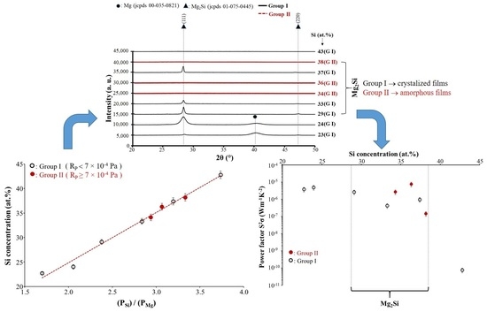
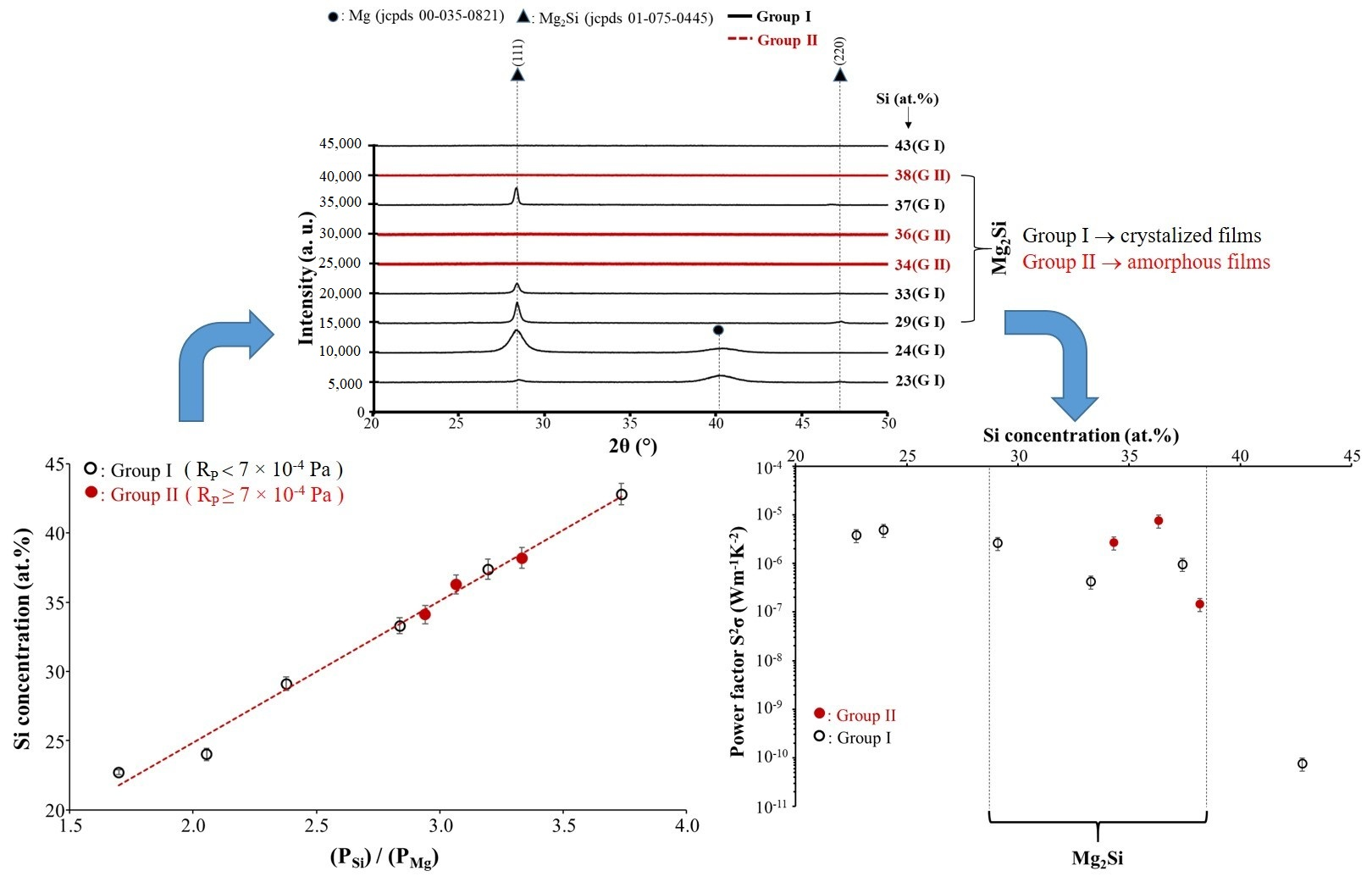
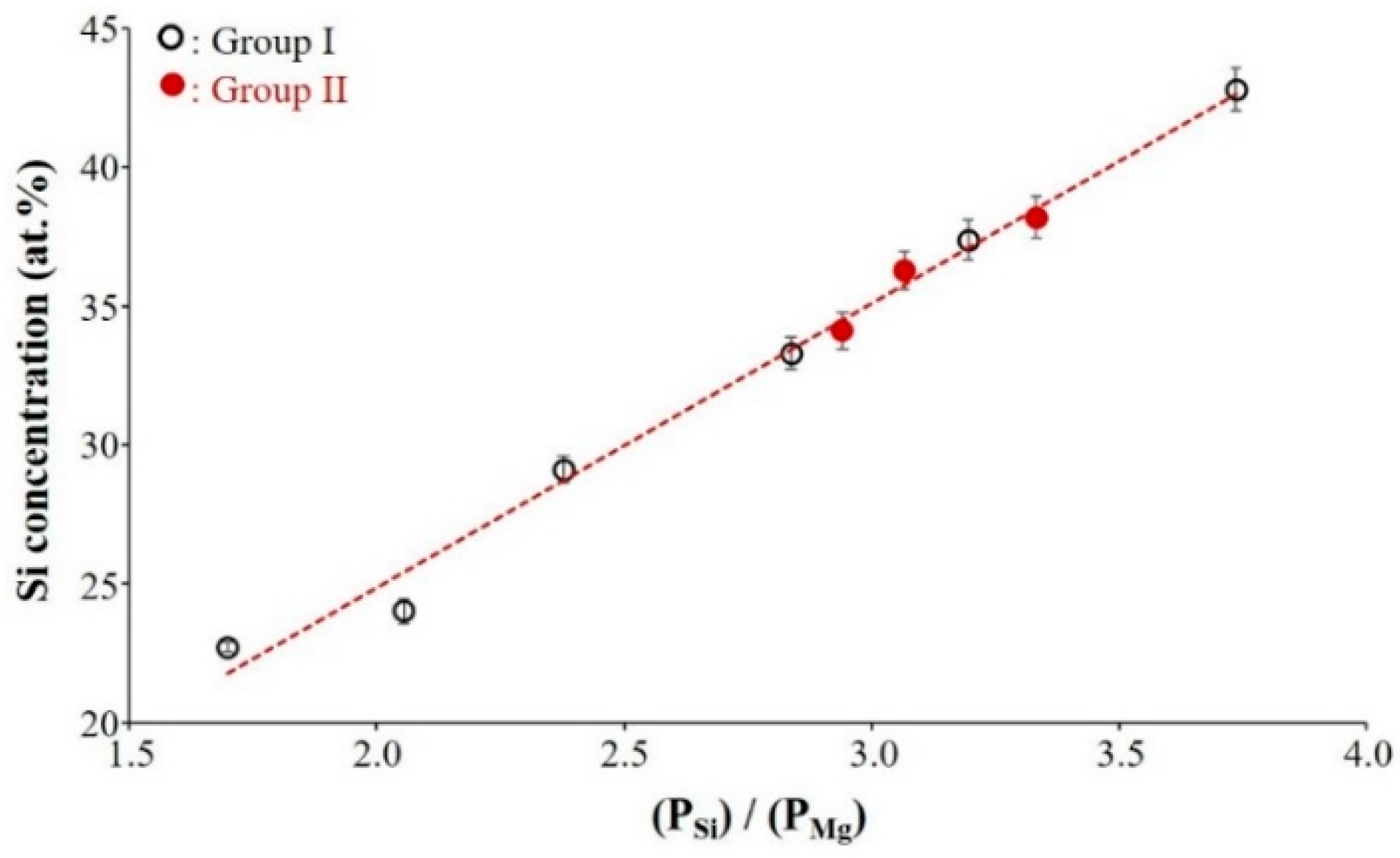
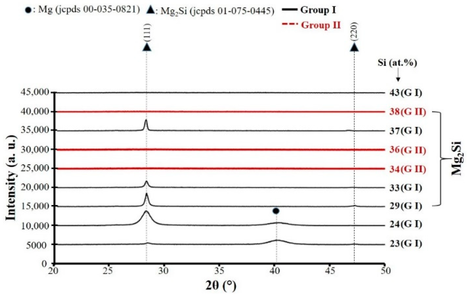
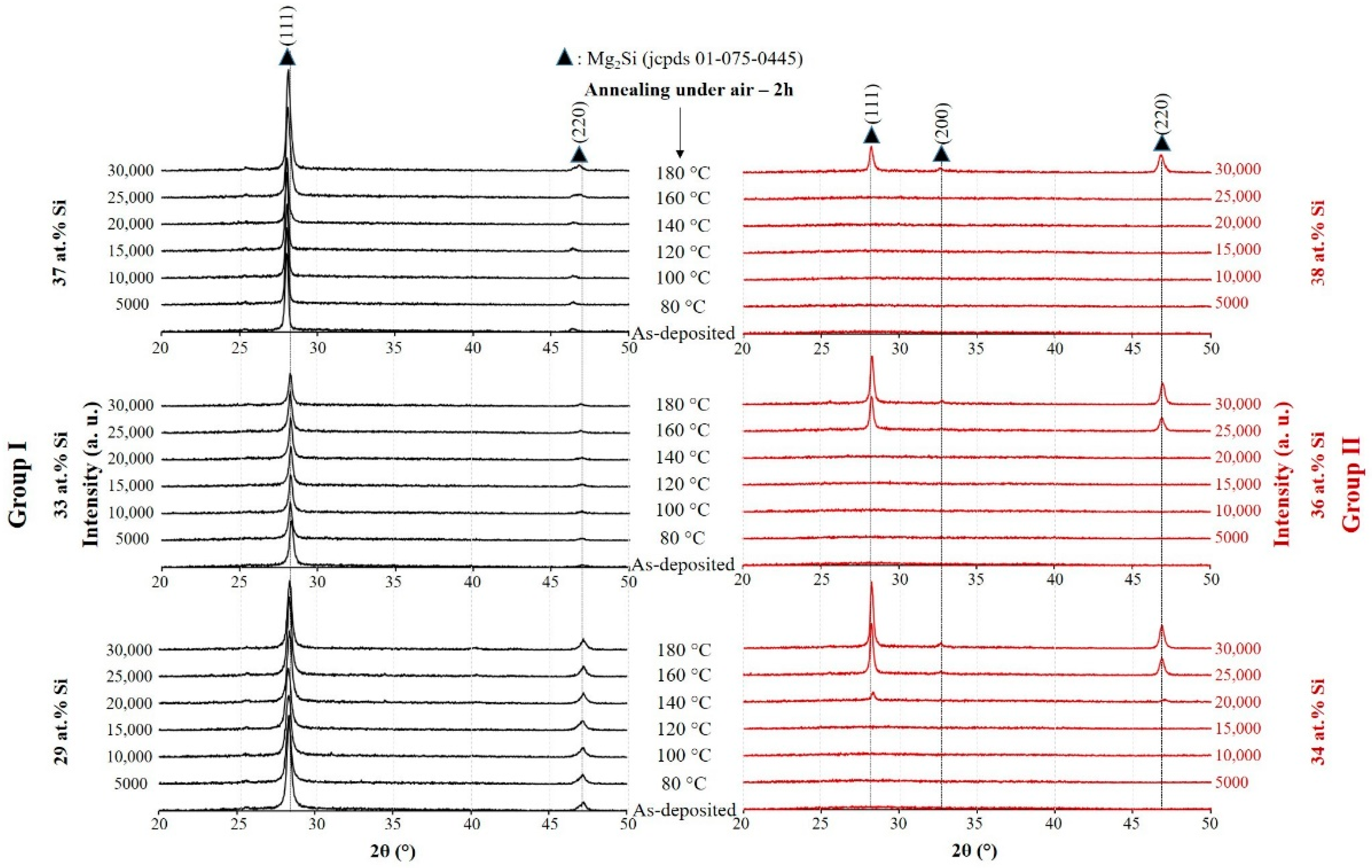
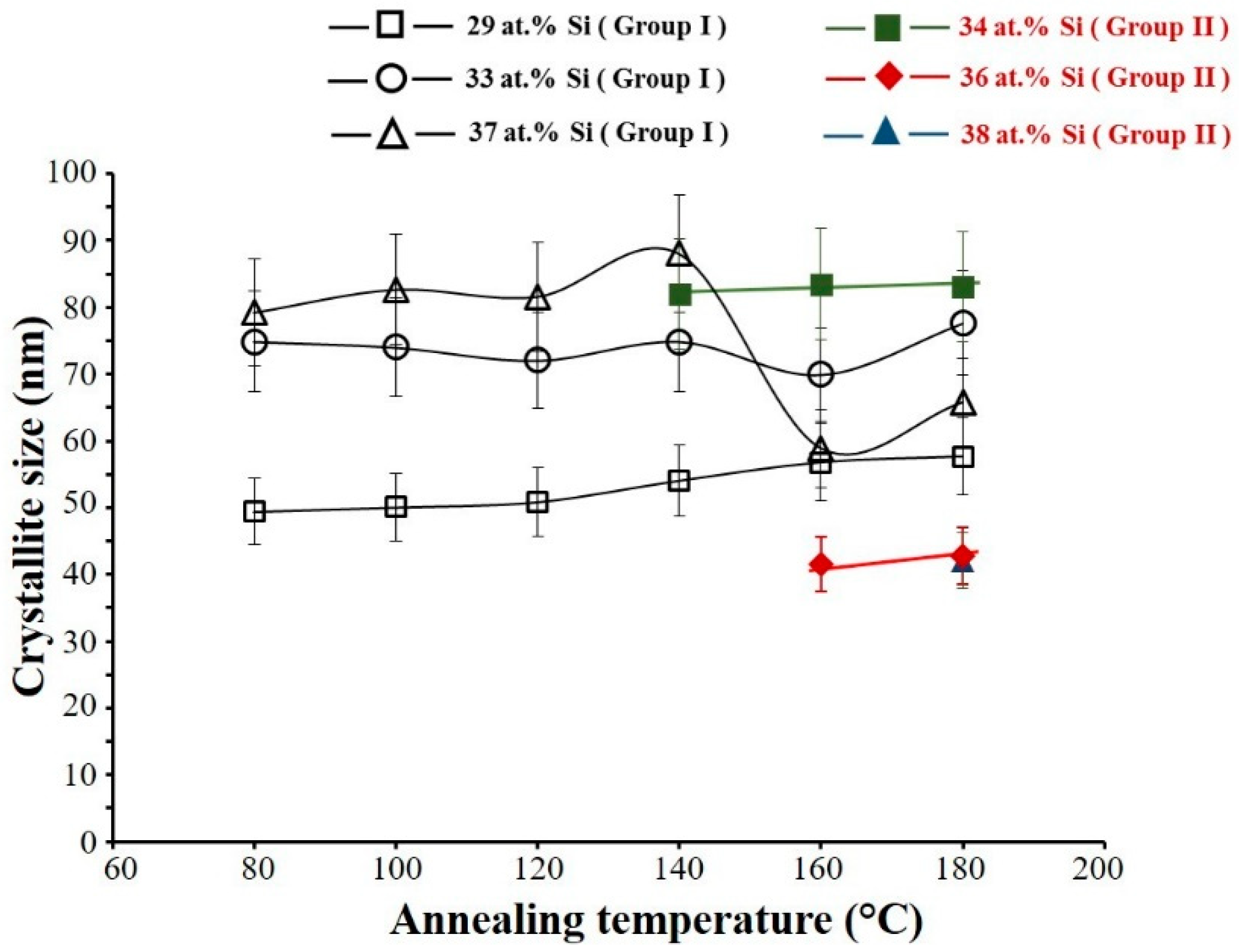
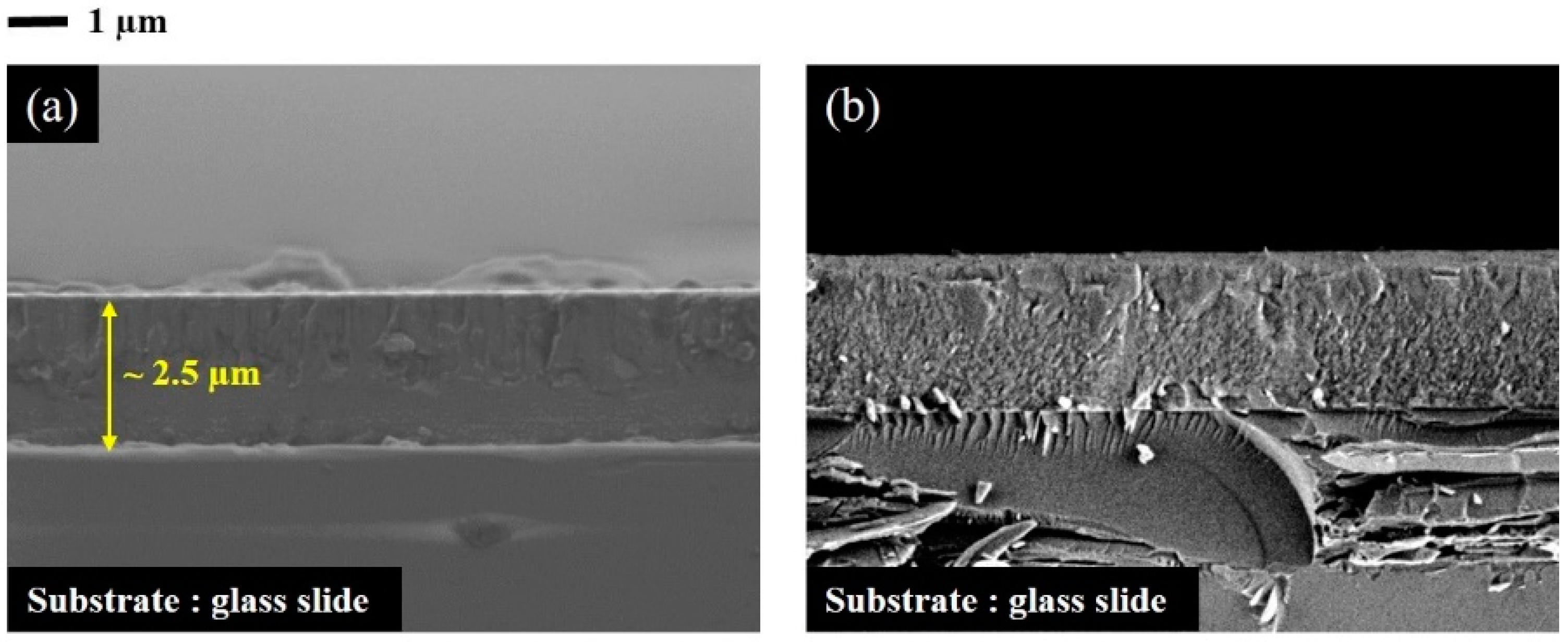
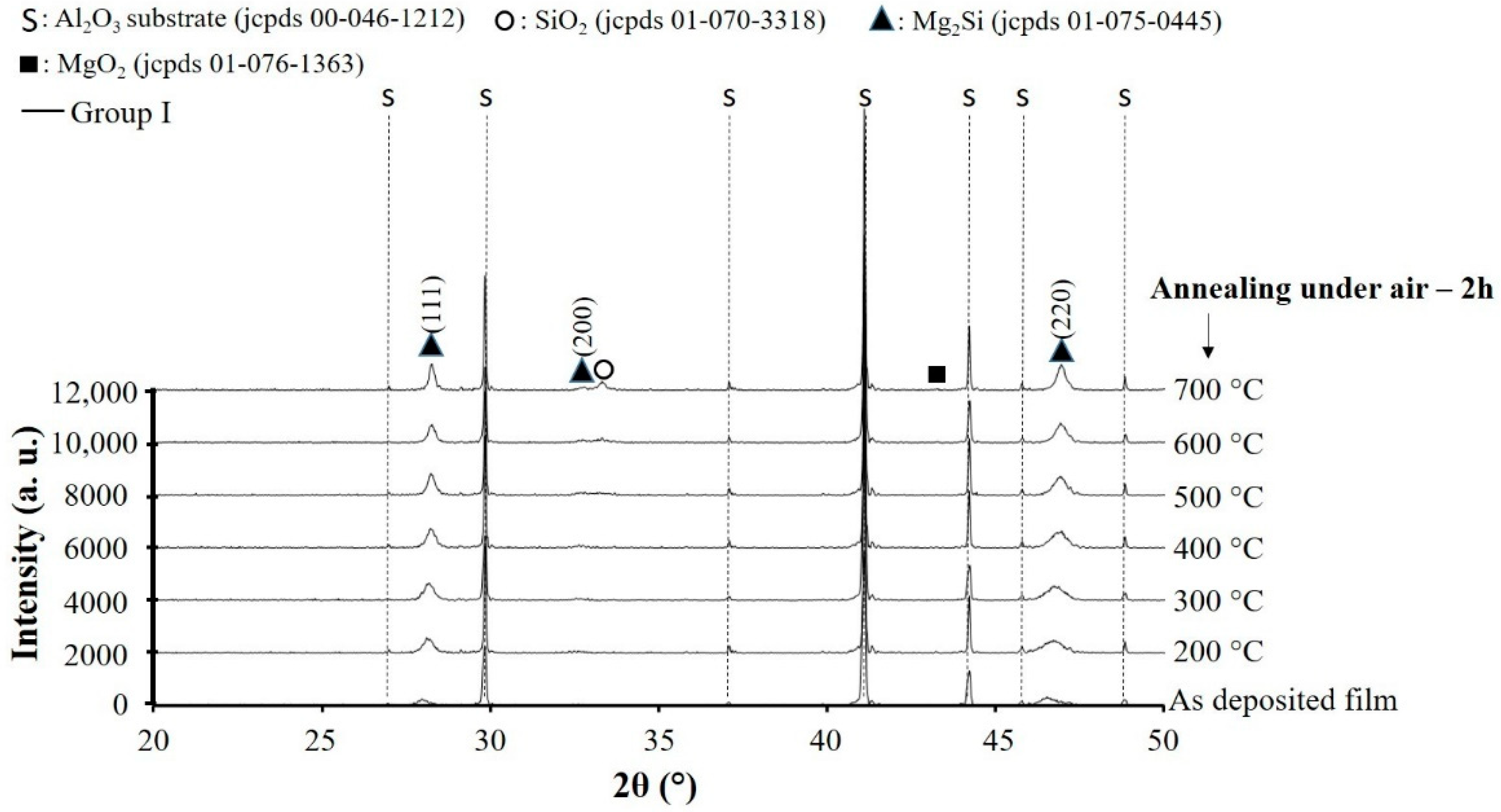
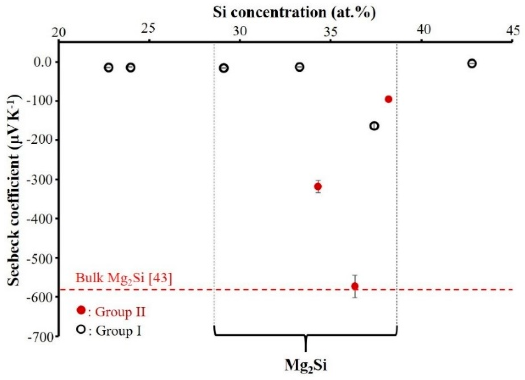
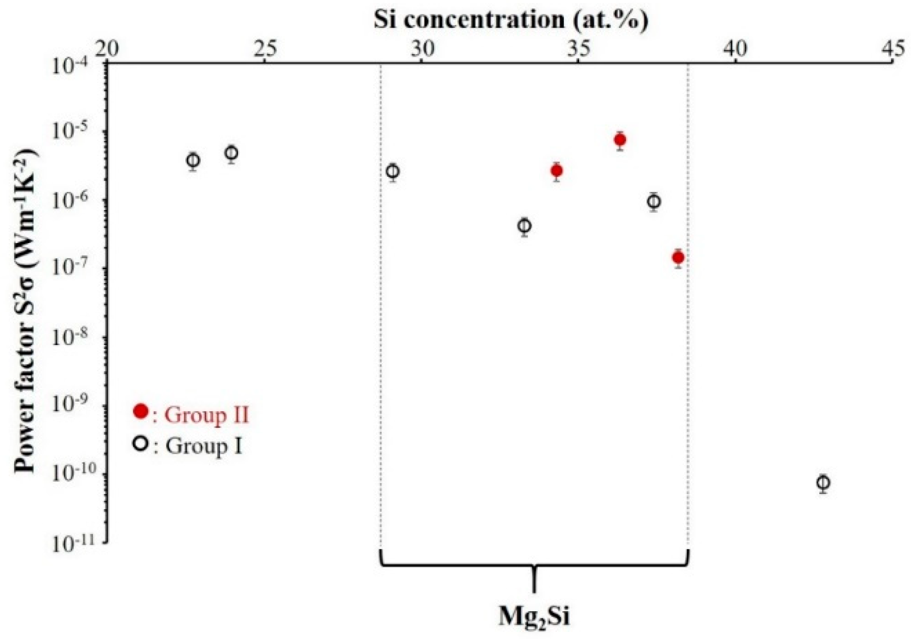
3. Results and Discussion

Figure 1 presents the atomic concentration of Si measured by EDS analysis in the different Mg–Si films as a function of sputtering power ratio applied to each target (PSi/PMg) during the deposition stage. These results show that the Si content in the films linearly increases with an increasing sputtering power ratio PSi/PMg. The open symbols and close red symbols represent Si at.% in the films synthesized with experimental conditions of Group I and Group II, respectively.
In order to study the evolution of the crystallographic structure vs. chemical composition of as-deposited coatings, X-ray diffraction analyses were systematically performed. Without annealing treatment, Figure 2 presents the structure of as-deposited Mg–Si films deposited on glass substrate. Black lines and red lines correspond to Group I and Group II, respectively. For the films deposited in Group I, and containing 23 at.% and 24 at.% Si, they exhibit (002) diffracted signal related to hexagonal close-packed Mg metal (jcpds # 00-035-821) at 2θ = 40.16° and another phase is related to the structure of face-centered cubic Mg2Si compound (jcpds # 01-075-0445) with (111) strong preferential orientation and Fm-3m space group. The relatively large full width at half maximum (FWHM) observed at about 28° for (111) Mg2Si peak confirms the existence of small crystallite size in this film. With increasing of Si concentration up to 33 at.%, the microstructure of the film is coarsened. The structure of Mg2Si achieved and kept with any trace of Mg phase while Si content changes from 29 to 37 at.%. By increasing further the Si content to value of about 43 at.% Si, Mg2Si structure leads to the formation of an amorphous structure (no diffracted signals). The addition of sufficient metalloid elements such as Si due to its fourfold coordination, is reported in the literature as an effective way to stabilize amorphous structure of sputter-deposited thin films [41,42].
The red lines are related to structure of the films deposited in group II. As shown in Figure 2, no matter their composition, all as-deposited films exhibit an amorphous structure. It is worth to note that when the residual pressure is higher than 7 × 10⁻⁴ Pa, the occurrence of oxygen, nitrogen, and/or hydrogen partial pressures in the rector and the interaction of these reactive species with Si and Mg sputtered particles during the deposition process strongly influence the films compactness and stabilizes the amorphous or nanocrystallized phase. The similar behavior is reported by incorporation of a few percentage of nitrogen into Al/Cr and Al/Ti coatings by Sanchette et al. [39].
Three samples of each group with the composition closed to Mg2Si (29 ≤ at.% Si ≤ 38) are selected for the next characterizations (selected zone in Figure 2). These films are annealed under air from 80 °C up to 180 °C and the evolution of the film structure are observed by XRD (Figure 3). For the films in Group I, no matter of the film composition and annealing temperature, the fcc structure of Mg2Si (jcpds # 01-075-0445) with (111) strong preferential orientation can be found on the patterns. It is important to note that for the films with at.% Si = 37 both peaks related to Mg2Si structure shift to lower Bragg angles (as-deposited film and the film annealed at temperature ≤ 140 °C). Such a behavior seems to indicate the presence of stress in this film and after annealing at temperature higher than 140 °C, both (111) and (220) peaks are shifted to their standard Mg2Si positions due to the relaxation of the film. As-deposited films in Group II exhibit an amorphous structure. As shown in Figure 3, the crystallization beginning depends on Si content in the films. The film with about 34 at.% Si adopts the Mg2Si phase after annealing under air at about 140 °C while for the film with 38 at.% Si, the temperature of crystallization increases to about 180 °C. The shift of the peaks to lower angles are not observed in the films of Group II no matter their compositions and the single Mg2Si phase found after post annealing treatment.
The FWHM of (111) peak at 2θ ≈ 28° is measured and according to Scherrer law, the crystallite size of the layers is calculated after annealing under air at different temperatures. In Group I, (Figure 4), the crystallite size of the film with 29 at.% Si increases from 50 nm to about 60 nm with rising of annealing temperature. The crystallite size of the film containing 33 at.% Si is not significantly changed with annealing treatment up to 140 °C and the average of crystallite size is about 75 ± 7.5 nm. After annealing at temperatures higher than 140 °C, no significant evolution of the crystallite size is observed for this sample. For the film with 37 at.% Si, crystallite size increases from 77 to 88 nm as the annealing temperature rises from 80 to 140 °C and the crystallite size drastically decreases to about 58 nm after annealing at higher temperatures.
The variation of the crystallite size in Group II, is also studied after the film crystallization as presented in Figure 4. The largest crystallite size of about 83 nm was also calculated for the film with 34 at.% Si. A further increase of Si content in the films of Group II reduces the crystallite size close to 42 nm.
Regarding the decrease of the crystallite size of sample with 37 at.% Si in Group I after annealing at the temperatures higher than 140 °C, this behavior seems quite weird because theoretically with increasing of annealing temperature the crystallite size should be increased. Considering the SEM cross section observations of this film before and after annealing in air at 180 °C for 2 h (Figure 5a,b, respectively) it is clear that as-deposited films are compact and a really dense morphology was observed for half part of this sample, whereas another part exhibits a columnar-like morphology (Figure 5a).
We believe, especially in the case of this sample, that amorphous and crystallized phases coexist for as-deposited film and during post annealing up to 140 °C. In this temperature range, the amorphous part remains stable. However, the crystallized part rises with a crystallite size growing from 77 nm to 88 nm as the annealing temperature changes from 80 °C to 140 °C. After annealing at the temperature higher than 140 °C, the amorphous part of this coating will be crystallized (with respect to the crystallization temperature determined in Figure 3 for the amorphous samples). The stress relaxation observed in Figure 2 after annealing at temperatures higher than 140 °C can be explained by this entirety crystallization and normally the average of crystallite size for totality of this layer will be decreased. The SEM observation of this sample after annealing in air at 180 °C for 2 h (Figure 5b) confirms our hypothesis. Annealed film presents homogenously fine crystallite morphology compared to as-deposited film.
Without any doubt, oxidation resistance plays a crucial role on thermoelectric performances of these coatings. In order to investigate oxidation resistance of these films, Mg2Si thin films with suitable composition deposited on alumina substrate were post-annealed in air during 2 h at temperatures up to 700 °C. This annealing treatment was followed by XRD analysis. The X-ray diffraction patterns are collected and the results are shown in Figure 6. All diffracted peaks due to alumina substrate are identified by “s” symbol and face-centered cubic Mg2Si phase (jcpds # 01-075-0445) without any trace of secondary phase is detected for as-deposited film on alumina substrate. Increasing the annealing temperature up to 700 °C, the narrowing of FWHM confirms the film grain size growth. For the film annealed at temperature >500 °C, oxidation of Mg2Si superficial layer gives rise to the formation of SiO2 secondary phase with a diffracted signal at 2θ ≈ 33.48° and a very low intensity peak of MgO2 at 2θ ≈ 43.39°. The presence of SiO2 and MgO2 as insulator secondary phases at the surface of the coating prohibits the electrical resistivity measurements.
Top surface, X-ray mapping and brittle fracture cross-section of Mg2Si film on Al2O3 substrate before and after post-annealing in air at 500 °C and 700 °C for 2 h are observed by SEM. Pictures reported in Figure 7 show that the surface microstructure of alumina substrate are perfectly and homogenously covered by as-deposited Mg2Si film. Sputtered thin film reproduces the same surface morphology and topography of alumina substrate (Figure 7a) with a good composition homogeneity (Figure 7b), and SEM cross-section showed relatively dense layer without cracks and delamination (Figure 7c).
After annealing at 500 °C (Figure 7d–f), it results in an even denser morphology and a coarsely crystallized film. From the top surface observation (Figure 7d,e), the SiO2 particles are evidently observed, in agreement with results obtained in Figure 6 but the film morphology is not really changed (Figure 7f). By increasing the annealing temperature up to 700 °C, it can be observed from the top image that Mg2Si layer is destroyed (Figure 7g) due to oxidation. The film morphology completely changes and as confirmed by X-ray mapping image (Figure 7h) inhomogeneous Si–O and Mg–O areas are formed. The SEM cross-section of the film annealed at 700 °C (Figure 7i), highlights the formation of nanoporosity in the film. After some inquiries in the matter, it has been established that the Mg2Si thin films are not thermally stable for temperatures >500 °C from the point of the view of morphology and structure. The films suffer superficial decomposition because of Mg and Si oxidation [33].
The variation of DC electrical resistivity of the films with different Si contents is presented as a function of the temperature (Figure 8). The films resistivity increases with a growing Si concentration in the films. This variation of the films resistivity vs. composition is more remarkable in the case of the films in Group I compared to that of the films in Group II.
Mg2Si films in Group II exhibit the typical behavior of semi-conducting materials, i.e., a decrease of the electrical resistivity as the temperature increases. The same behavior can be observed for the film with 37 at.% Si in Group I from room temperature up to 140 °C because of the presence of an amorphous part in this sample. For the temperatures higher than 140 °C, the films resistivity increases with the temperature augmentation. This unusual incidence seems to be in good agreement whit the crystallite size decreasing observed at the same temperature in Figure 4. This phenomenon is emphasized for the film with 33 at.% Si and as shown in Figure 8, the electrical resistivity increases drastically vs. temperature for the value higher than 120 °C. The origin of this resistivity variation is not clear and cannot be connected to the crystallite size variation or the presence of an amorphous part in this range of compositions. As shown in Figure 4, crystallite size of sample with 33 at.% Si remains relatively at the same level after annealing at different temperatures. Maybe absorption and desorption of humidity play an important role in this abnormous resistivity variations. Finally for the film with 29 at.% Si the film resistivity remains quite constant vs. temperature.
The variation of carrier concentration and mobility of the films with different Si contents are presented as a function of the temperature in Figure 9b. The film deposited in Group I with 29 at.% Si exhibits the highest free carrier concentration (from 2.09 × 10²⁰ to 2.45 × 1019 cm−3). For the film with 33 at.% Si, an important decrease of carrier concentration occurs with temperature increasing higher than 110 °C (Figure 9a). The same variation is observed for the carrier concentration of the film containing 37 at.% Si. Up to 110 °C the carrier concentration increases and then decreased for the higher temperature. Films deposited in Group II generally exhibit lower carrier concentration in comparison with these deposited in Group I. The highest carrier mobility observed for the film with 33 at.% Si in Group I, from 1.4 × 102 cm2 V−1 s−1 to about 1.3 × 103 cm2 V−1 s−1 as the temperature varied from 30 to 182 °C. For this range of temperatures, a decrease of mobility vs. temperature could be expected due to lattice scattering phenomenon, as typically reported in semiconducting materials. However, our sputter-deposited films certainly contain a high concentration of growth defects. They act as impurities and the temperature dependence of mobility rather exhibits an evolution connected to the impurity scattering mechanism, i.e., an increase of mobility with the temperature.
Room temperature electrical conductivity of Mg–Si films as a function of Si atomic concentration is shown in Figure 10. The electrical conductivity of the films of Group I, decreases while the atomic percentage of Si increases. The film with 24 at. % Si presents the highest electrical conductivity (σ = 2.86 × 10⁴ Ω−1 m−1). The film conductivity drastically decreases by about four orders of magnitude and reaches the lowest value of σ ≈ 4.39 Ω−1 m−1 while the Si content is about 43 at.%. This enhancement of resistivity for the film with about 43 at.% Si, is related to the amorphous structure and excess of Si in the film composition. For amorphous coatings of Group II (red symbols), the same phenomena are observed. The film conductivity decreases with increasing Si content.
The comparison between the films of Groups I and II with relatively the same composition allows us estimating beneficial or detrimental effects of crystallized or amorphous structure on electrical conductivity. For example, the electrical conductivity decreases for amorphous Mg2Si coating down to 2.64 × 101 Ω−1 m−1 in comparison with crystallized films of Group I (σ = 2.62 × 10³ Ω−1 m−1 with nearly the same composition). It is worth noting that room temperature electrical conductivity reported in literature for bulk Mg2Si is about 1.4 × 10³ Ω−1 m−1 [43].
The Seebeck coefficient of Mg–Si thin films measured at room temperature as a function of Si content is shown in Figure 11. All Seebeck coefficients are negative, as expected for n-type semiconductors. Except for the film with 37 at.% Si (−163 µV K−1 Seebeck value), no matter their composition, the films deposited in Group I exhibit a very low Seebeck coefficient (a few −10 µV K−1). Hatched zone indicates Mg2Si structure (29 ≤ at.% Si ≤ 38) and we believed the reason of high Seebeck value measured especially for the sample with 37 at.% Si in Group I should be related to the coexistence of amorphous and crystallized Mg2Si phases.
The films of Group II coefficients are significantly higher than those of Group I. The highest Seebeck coefficient (absolute value) of 574 µV K−1 is measured for the film with 36 at.% Si. The Seebeck coefficient reported in the literature for thin film seems to be much lower than for bulk materials [43]. In this study, the maximum Seebeck coefficient measured for Mg2Si thin film at room temperature is relatively close to the reported values of ~580 µV K−1 for the bulk materials [43]. As shown in Table 1, the residual pressure for the films deposited in Group II was higher than that of Group I. We believe that, for the films of Group II, the existence of residual oxygen, nitrogen, and/or hydrogen gases inside the reactor leads to the deposition of Mg2Si thin films with O, N, and/or H as impurity elements. The presence of these impurity elements has a noticeable influence on amorphous structure formation. They generate interstitial defects leading to high Seebeck coefficient and low electrical conductivity. A deeper investigation is required with perfect monitoring of oxygen, nitrogen, and/or hydrogen partial pressures during deposition of the film to confirm the precise role of these impurity elements.
The power factor PF (Equation (2)) is defined as the ability to produce useful electrical power by thermoelectric materials. The optimization of the thermoelectric material properties is possible by enhancement of the power factor and reduction of the thermal conductivity. “An ideal thermoelectric material should have a low lattice thermal conductivity (like a glass or an amorphous material), and a high electrical conductivity (like a crystal)” [23]. Figure 12 shows the power factor of the films at room temperature as a function of their composition.
As depicted in Figure 12, generally the PF value of the Mg–Si thin films in Group I, decreases with a raising Si content in the films. In selected zone, the best power factor of Mg2Si thin films is obtained for 29 at.% Si with PF value of about 2 × 10⁻⁶ W m−1 K−2. The power factor decreases for the sample with 33 at.% Si and is significantly enhanced for the film with 37 at.% Si. We believe the PF achieves a value of around 9.7 × 10⁻⁷ W m−1 K−2 because amorphous and crystallized phases coexist for as-deposited film with 37 at.% Si. For the films of Group II, the evolution of power factor is not similar to that of Group I. The maximum PF value of 7.6 × 10⁻⁶ W m−1 K−2 was obtained for the film with 36 at.% of Si. It is important to notice that in relatively similar range of compositions, Mg2Si thin films of Group II reveal significantly higher values of PF compared to those of Group I.
In this study, the power factor of thin films remains low because of the weak electrical conductivity of the films in comparison with the bulk materials. The typical range of power factors reported in the literature for bulk materials is about 3.7 × 10⁻⁴ W m−1 K−2 [43].

4. Conclusions

Mg–Si thin films were deposited by co-sputtering of Mg and Si targets by adjusting the power applied on each target. The chemical composition of the films was precisely controlled and two groups of thin films were prepared. In the first group, residual pressure of the reactor was lower than 7 × 10⁻⁴ Pa and in the second group, the sputtering chamber was pumped down to a base pressure higher than the critical value of 7 × 10⁻⁴ Pa. The influence of this residual pressure as well as the film composition on structural, morphological, and thermoelectric properties of the films was discussed. It was shown that the film microstructure and electrical and thermoelectric properties are strongly affected by the residual pressure. Not including the film with 43 at.% Si, all as-deposited films of Group I were crystallized while an amorphous structure was obtained for all as-deposited films of Group II (no matter their composition). For both groups, the film conductivity decreased with increasing the Si content and room temperature electrical conductivity decreased about two orders of magnitude for amorphous Mg2Si coatings of Group II (σ ≈ 26.4 Ω−1 m−1) in comparison with crystallized thin films of Group I (σ ≈ 2.62 × 10³ Ω−1 m−1) with nearly the same composition. The films deposited in Group I exhibited generally poor Seebeck coefficients (α ≈ −10 µV K−1) and only for the film with 37 at.% Si the absolute Seebeck value reached 164 µV K−1 and power factor enhanced to 9.7 × 10⁻⁷ W m−1 K−2. Amorphous and crystallized phases coexisted for as-deposited film with 37 at.% Si and the presence of an amorphous phase explains this higher thermoelectric property of this film compared to another coating of Group I.
The highest absolute Seebeck coefficient of 574 µV K−1 and maximum power factor of 7.6 × 10⁻⁶ W m−1 K−2 were measured for the films of Group II with about 36 at.% of Si. The results of this paper highlight the possibility to improve the thermoelectric power factor of Mg2Si thin films with amorphous state by a fine tuning of residual pressure and composition. The amorphous state persists during an annealing treatment in air of up to 140 °C. After annealing at temperatures higher than 500 °C in air, superficial oxidation of Mg2Si layer gives rise to the formation of SiO2 and MgO2 insulator secondary phases which prohibit electrical resistivity measurements. As an additional conclusion, it is important to note that, conduction mechanism in Mg2Si films still remains an open question and requires more investigations.

Author Contributions

Conceptualization, C.P. and K.N.; Data Curation, M.A.P.Y. and N.M.; Formal Analysis, N.M.; Funding Acquisition, M.A.P.Y., F.P., F.C. and A.B.; Investigation, M.A.P.Y.; Supervision, A.B.; Writing–Original Draft, M.A.P.Y., F.P., F.C. and N.M.; Writing–Review & Editing, N.M., F.P., F.C. and A.B.

Funding

The research was funded by “Région Bourgogne-Franche Comté” and “Pays de Montbéliard Agglomération” (No. 2016Y-04501) in the frame of the MOBILITECH project.

Conflicts of Interest

The authors declare no conflict of interest. The founding sponsors had no role in the design of the study; in the collection, analyses, or interpretation of data; in the writing of the manuscript, or in the decision to publish the results.

References

  1. Lopez, J.; Rios, R.; Bao, F.; Wang, G. Evolving privacy: From sensors to the Internet of Things. Future Gener. Comput. Syst. 2017, 75, 46–57. [Google Scholar] [CrossRef]
  2. Bello, O.; Zeadally, S. Toward efficient smartification of the Internet of Things (IoT) services. Future Gener. Comput. Syst. 2017, in press. [Google Scholar] [CrossRef]
  3. Guerrero-Ibanez, J.A.; Zeadally, S.; Contreras-Castillo, J. Integration challenges of intelligent transportation systems with connected vehicle, cloud computing, and internet of things technologies. IEEE Wirel. Commun. 2015, 22, 122–128. [Google Scholar] [CrossRef]
  4. Liu, Y.; Cui, J. Design and implementation of human health monitoring platform based on internet of things technology. In Proceedings of the 2017 IEEE International Conference on Computational Science and Engineering (CSE) and IEEE International Conference on Embedded and Ubiquitous Computing (EUC), Guangzhou, China, 21–24 July 2017; pp. 422–425. [Google Scholar]
  5. Iezzi, B.; Ankireddy, K.; Twiddy, J.; Losego, M.D.; Jur, J.S. Printed, metallic thermoelectric generators integrated with pipe insulation for powering wireless sensors. Appl. Energy 2017, 208, 758–765. [Google Scholar] [CrossRef]
  6. Selinger, M.; Sepulveda, A.; Buchan, J. Education and the Internet of Everything: How Ubiquitous Connectedness Can Help Transform Pedagogy; Cisco: San Jose, CA, USA, 2013. [Google Scholar]
  7. Iannacci, J. Microsystem based Energy Harvesting (EH-MEMS): Powering pervasivity of the Internet of Things (IoT)—A review with focus on mechanical vibrations. J. King Saud Univ. Sci. 2017, in press. [Google Scholar] [CrossRef]
  8. Nakagawa, K.; Suzuki, T. A High-Efficiency thermoelectric module with phase change material for IoT power supply. Proc. Eng. 2016, 168, 1630–1633. [Google Scholar] [CrossRef]
  9. He, W.; Zhang, G.; Zhang, X.; Ji, J.; Li, G.; Zhao, X. Recent development and application of thermoelectric generator and cooler. Appl. Energy 2015, 143, 1–25. [Google Scholar] [CrossRef]
  10. Hsu, K.F.; Loo, S.; Guo, F.; Chen, W.; Dyck, J.S.; Uher, C.; Hogan, T.; Polychroniadis, E.K.; Kanatzidis, M.G. Cubic AgPbmSbTe2+m: Bulk thermoelectric materials with figure of merit. Science 2004, 303, 818–821. [Google Scholar] [CrossRef] [PubMed]
  11. Biswas, K.; He, J.; Blum, I.D.; Wu, C.I.; Hogan, T.P.; Seidman, D.N.; Dravid, V.P.; Kanatzidis, M.G. High-performance bulk thermoelectrics with all-scale hierarchical architectures. Nature 2012, 489, 414–418. [Google Scholar] [CrossRef] [PubMed]
  12. Zhang, X.; Zhao, L. Thermoelectric materials: Energy conversion between heat and electricity. J. Materiomics 2015, 1, 92–105. [Google Scholar] [CrossRef]
  13. Poudel, B.; Hao, Q.; Ma, Y.; Lan, Y.; Minnich, A.; Yu, B.; Yan, X.; Wang, D.; Muto, A.; Vashaee, D.; Chen, X.; Liu, J.; Dresselhaus, M.S.; Chen, G.; Ren, Z. High-thermoelectric performance of nanostructured bismuth antimony telluride bulk alloys. Science 2008, 320, 634–638. [Google Scholar] [CrossRef] [PubMed]
  14. Shen, J.; Zhu, T.; Zhao, X.; Zhang, S.; Yang, S.; Yin, Z. Recrystallization induced in situ nanostructures in bulk bismuth antimony tellurides: A simple top down route and improved thermoelectric properties. Energy Environ. Sci. 2010, 3, 1519–1523. [Google Scholar] [CrossRef]
  15. Heremans, J.P.; Jovovic, V.; Toberer, E.S.; Saramat, A.; Kurosaki, K.; Charoenphakdee, A.; Yamanaka, S.; Snyder, G.J. Enhancement of thermoelectric efficiency in PbTe by distorsion of the electronic density of states. Science 2008, 321, 554–557. [Google Scholar] [CrossRef] [PubMed]
  16. Biswas, K.; He, J.; Zhang, Q.; Wang, G.; Uher, C.; Dravid, V.P.; Kanatzidis, M.G. Strained endotaxial nanostructures with high thermoelectric figure of merit. Nat. Chem. 2011, 3, 160–166. [Google Scholar] [CrossRef] [PubMed]
  17. Sun, X.; Gao, K.; Pang, X.; Yang, H.; Volinsky, A.A. Structure and composition effects on electrical and optical properties of sputtered PbSe thin films. Thin Solid Films 2015, 592, 59–68. [Google Scholar] [CrossRef]
  18. Daniel, M.V.; Friedemann, M.; Franke, J.; Albrecht, M. Thermal stability of thermoelectric CoSb3 skutterudite thin films. Thin Solid Films 2015, 589, 203–208. [Google Scholar] [CrossRef]
  19. Saiga, Y.; Du, B.; Deng, S.K.; Kajisa, K.; Takabatake, T. Thermoelectric properties of type-VIII clathrate Ba8Ga16Sn30 doped with Cu. J. Alloy. Compd. 2012, 537, 303–307. [Google Scholar] [CrossRef]
  20. Toberer, E.S.; Cox, C.A.; Brown, S.R.; Ikeda, T.; May, A.F.; Kauzlarich, S.M.; Snyder, G.J. Traversing the metal-insulator transition in a Zintl phase: Rational enhancement of thermoelectric efficiency in Yb14Mn1−xAlxSb11. Adv. Funct. Mater. 2008, 18, 2795–2800. [Google Scholar] [CrossRef]
  21. Yan, X.; Liu, W.; Wang, H.; Chen, S.; Shiomi, J.; Esfarjani, K.; Wang, H.; Wang, D.; Chen, G.; Ren, Z. Stronger phonon scattering by larger differences in atomic mass and size p-type half-Heuslers Hf1−xTixCoSb0.8Sn0.2. Energy Environ. Sci. 2012, 5, 7543–7548. [Google Scholar] [CrossRef]
  22. Chen, S.; Lukas, K.C.; Liu, W.; Opeil, C.P.; Chen, G.; Ren, Z. Effect of Hf concentration on thermoelectric properties of nanostructured n-type Half-Heusler materials HfxZr1-xNiSn0.99Sb0.01. Adv. Energy Mater. 2013, 3, 1210–1214. [Google Scholar] [CrossRef]
  23. Bashir, M.B.A.; Said, S.M.; Sabri, M.F.M.; Shnawah, D.A.; Elsheikh, M.H. Recent advances on Mg2Si1−xSnx materials for thermoelectric generation. Renew. Sustain. Energy Rev. 2014, 37, 569–584. [Google Scholar] [CrossRef]
  24. Prahoveanu, C.; Lacoste, A.; Bechu, S.; Vaulx, C.D.; Azzouz, K.; Laversenne, L. Investigation of Mg2(Si,Sn) thin films for integrated thermoelectric devices. J. Alloy. Compd. 2015, 649, 573–578. [Google Scholar] [CrossRef]
  25. Zhang, Q.; Zheng, Y.; Su, X.; Yin, K.; Tanga, X.; Uher, C. Enhanced power factor of Mg2Si0.3Sn0.7 synthesized by a non-equilibrium rapid solidification method. Scr. Mater. 2015, 96, 1–4. [Google Scholar] [CrossRef]
  26. Quoc, H.L.; Lacoste, A.; Béchu, S.; Bès, A.; Bourgault, D.; Fruchart, D. Deposition of thin films of Mg2Si1−xSnx solid solution by plasma-assisted co-sputtering. J. Alloy. Compd. 2012, 538, 73–78. [Google Scholar] [CrossRef]
  27. Murtaza, G.; Sajid, A.; Rizwan, M.; Takagiwa, Y.; Khachai, H.; Jibran, M.; Khenata, R.; Omran, S.B. First principles study of Mg2X (X = Si, Ge, Sn, Pb):Elastic, optoelectronic and thermoelectric properties. Mater. Sci. Semicond. Process. 2015, 40, 429–435. [Google Scholar] [CrossRef]
  28. Gao, H.; Zhu, T.; Zhao, X.; Deng, Y. Variations of thermoelectric properties of Mg2.2Si1-ySny-0.013Sb0.013 materials with different Si/Sn ratios. J. Solid State Chem. 2014, 220, 157–162. [Google Scholar] [CrossRef]
  29. Quoc, H.L.; Béchu, S.; Populoh, S.; Weidenkaff, A.; Lacoste, A. Thermoelectric properties of thin films of Sb doped Mg2Si1−xSnx solid solutions. J. Alloy. Compd. 2013, 546, 138–144. [Google Scholar] [CrossRef]
  30. Songa, R.B.; Aizawa, T.; Sun, J.Q. Synthesis of Mg2Si1−xSnx solid solutions as thermoelectric materials by bulk mechanical alloying and hot pressing. Mater. Sci. Eng. B Solid State Mater. 2007, 136, 111–117. [Google Scholar] [CrossRef]
  31. Hu, X.; Barnett, M.R.; Yamamoto, A. Synthesis of Al-doped Mg2Si1−xSnx compound using magnesium alloy for thermoelectric application. J. Alloy. Compd. 2015, 649, 1060–1065. [Google Scholar] [CrossRef]
  32. Liu, W.; Jie, Q.; Kim, H.S.; Ren, Z. Current progress and future challenges in thermoelectric power generation: From materials to devices. Acta Mater. 2015, 87, 357–376. [Google Scholar] [CrossRef] [Green Version]
  33. Kogut, I.; Record, M.C. Magnesium silicide thin film formation by reactive diffusion. Thin Solid Films 2012, 522, 149–158. [Google Scholar] [CrossRef]
  34. Serikawa, T.; Henmi, M.; Yamaguchi, T.; Oginuma, H.; Kondoh, K. Depositions and microstructures of Mg–Si thin film by ion beam sputtering. Surf. Coat. Technol. 2006, 200, 4233–4239. [Google Scholar] [CrossRef]
  35. Tani, J.I.; Kido, H. Electrical properties of Mg2Si thin films on flexible polyimide substrates fabricated by radio-frequency magnetron sputtering. J. Ceram. Soc. Jpn. 2015, 123, 298–301. [Google Scholar] [CrossRef]
  36. Prahoveanu, C.; Lacoste, A.; Vaulx, C.; Azzouz, K.; Salau, M.; Liu, Y.; Tainoff, D.; Bourgeois, O.; Laversenne, L. Effect of texture on the structural and transport properties of Sb-doped Mg2Si thin films. J. Alloy. Compd. 2016, 688, 195–201. [Google Scholar] [CrossRef]
  37. Ogawa, S.; Katagiri, A.T.; Shimizu, T.; Matsushima, M.; Akiyama, K.; Kimura, Y.; Uchida, H.; Funakubo, H. Electrical properties of (110)-oriented nondoped Mg2Si films with p-type conduction prepared by RF magnetron sputtering. J. Electron. Mater. 2014, 43, 2269–2273. [Google Scholar] [CrossRef]
  38. Creus, J.; Billard, A.; Sanchette, F. Corrosion behaviour of amorphous Al–Cr and Al–Cr–(N) coatings deposited by dc magnetron sputtering on mild steel substrate. Thin Solid Films. 2004, 466, 1–9. [Google Scholar] [CrossRef]
  39. Sanchette, F.; Loi, T.H.; Billard, A.; Frantz, C. Structure-properties relationship of metastable AI–Cr and AI–Ti alloys deposited by R.F. magnetron sputtering: Role of nitrogen. Surf. Coat. Technol. 1995, 74–75, 903–909. [Google Scholar] [CrossRef]
  40. Zhou, A.; Wang, W.; Yao, X.; Yang, B.; Li, J.; Zhao, Q.; Wang, C.; Xu, D.; Ziolkowski, P.; Mueller, E. Impact of the film thickness and substrate on the thermopower measurement of thermoelectric films by the potential-Seebeck microprobe (PSM). Appl. Therm. Eng. 2016, 107, 552–559. [Google Scholar] [CrossRef]
  41. Veprek, S.; Veprek-Heijman, M.G.J.; Karvankova, P.; Prochazka, J. Different approaches to superhard coatings and nanocomposites. Thin Solid Films 2005, 476, 1–29. [Google Scholar] [CrossRef]
  42. Yazdi, M.A.P.; Lomello, F.; Wang, J.; Sanchette, F.; Dong, Z.; White, T.; Wouters, Y.; Schuster, F.; Billard, A. Properties of TiSiN coatings deposited by hybrid HiPIMS and pulsed–DC magnetron co-sputtering. Vacuum 2014, 109, 43–51. [Google Scholar] [CrossRef]
  43. Kido, H. Thermoelectric properties of Bi-doped Mg2Si semiconductors. Phys. B Condens. Matter. 2005, 364, 218–224. [Google Scholar] [CrossRef]
Figure 1. Evolution of the Si atomic concentration in the films measured by Energy-Dispersive X-ray Spectroscopy (EDS) analysis vs. sputtering power ratio applied to each target. (Group I: RP < 7 × 10⁻⁴ Pa and Group II: RP ≥ 7 × 10⁻⁴ Pa).
Coatings 08 00380 g001
Figure 2. X-ray diffraction patterns of as-deposited Mg–Si thin films on glass slide substrate (Group I: RP < 7 × 10⁻⁴ Pa black lines and Group II: RP ≥ 7 × 10⁻⁴ Pa red lines). (Selected zone indicates the X-ray diffraction patterns of the films with the composition closed to Mg2Si).
Coatings 08 00380 g002
Figure 3. X-ray diffraction patterns of the films deposited on glass substrate after annealing in air for 2 h at different temperatures. (Group I: RP < 7 × 10⁻⁴ Pa and Group II: RP ≥ 7 × 10⁻⁴ Pa).
Coatings 08 00380 g003
Figure 4. Crystallite size of the films measured by Scherrer law as a function of annealing temperature. (Group I: RP < 7 × 10⁻⁴ Pa and Group II: RP ≥ 7 × 10⁻⁴ Pa).
Coatings 08 00380 g004
Figure 5. SEM cross-section observations of sample with 37 at.% Si deposited in Group I with RP < 7 × 10⁻⁴ Pa: (a) as-deposited and (b) annealed film in air at 180 °C for 2 h. An average of 2.5 µm was measured for the film thickness.
Coatings 08 00380 g005
Figure 6. X-ray diffraction patterns of Mg2Si coating with suitable composition in Group I (RP < 7 × 10⁻⁴ Pa) deposited on alumina substrate and post annealed in air for 2 h at different temperatures.
Coatings 08 00380 g006
Figure 7. Top, X-ray mapping and cross-section observations of Mg2Si thin films with suitable composition in Group I (RP < 7 × 10⁻⁴ Pa) deposited on alumina substrate; as-deposited (ac); annealed for 2 h at 500 °C (df) and 700 °C (gi) in air.
Coatings 08 00380 g007
Figure 8. DC electrical resistivity of Mg2Si films vs. temperature for different Si atomic concentrations. (Group I: RP < 7 × 10⁻⁴ Pa and Group II: RP ≥ 7 × 10⁻⁴ Pa).
Coatings 08 00380 g008
Figure 9. Carrier concentration (a) and carrier mobility (b) of Mg2Si films vs. temperature for different Si atomic concentrations. (Group I: RP < 7 × 10⁻⁴ Pa and Group II: RP ≥ 7 × 10⁻⁴ Pa).
Coatings 08 00380 g009
Figure 10. Room temperature electrical conductivity of Mg–Si thin films deposited on glass substrate vs. Si atomic concentration. (Selected zone indicates room temperature electrical conductivity of coatings with the composition closed to Mg2Si). (Group I: RP < 7 × 10⁻⁴ Pa and Group II: RP ≥ 7 × 10⁻⁴ Pa).
Coatings 08 00380 g010
Figure 11. Room temperature Seebeck coefficients of Mg–Si thin films deposited on glass substrate as a function of Si content. (Selected zone indicates room temperature Seebeck coefficients of coatings with the composition closed to Mg2Si). (Group I: RP < 7 × 10⁻⁴ Pa and Group II: RP ≥ 7 × 10⁻⁴ Pa).
Coatings 08 00380 g011
Figure 12. Power factor (PF) of Mg–Si thin films deposited on glass substrate vs. Si atomic concentration. (Selected zone indicates power factor of coatings with the composition closed to Mg2Si). (Group I: RP < 7 × 10⁻⁴ Pa and Group II: RP ≥ 7 × 10⁻⁴ Pa).
Coatings 08 00380 g012
Table 1. Sputtering parameters maintained during deposition of Mg–Si coatings.
TargetDischarge Power (W)Frequency (kHz)Toff (µs)Ar Flow Rate (sccm)Working Pressure (Pa)Run Duration (min)Draw Distance (DT-S) (mm)Residual Pressure, RP (Pa)
Group IGroup II
Si250–550605200.27585RP < 7 × 10⁻⁴RP ≥ 7 × 10⁻⁴
Mg146–150

