Mechanical Properties and Oxidation Behavior of Multilayered Hf–Si–N Coatings

Abstract
:1. Introduction
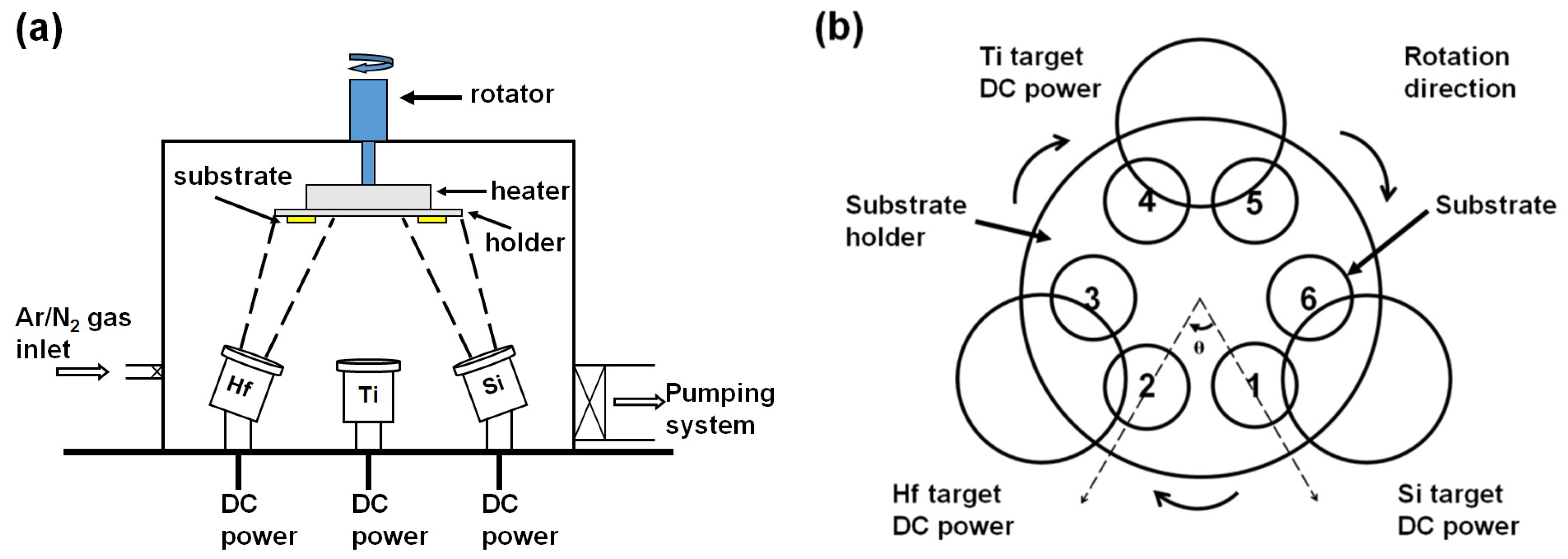
2. Materials and Methods
3. Results
3.1. As-Deposited Hf–Si–N Coatings
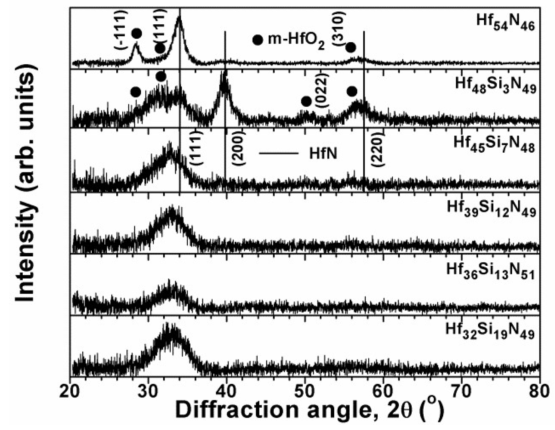
3.1.1. Monolithic Hf–Si–N Coatings
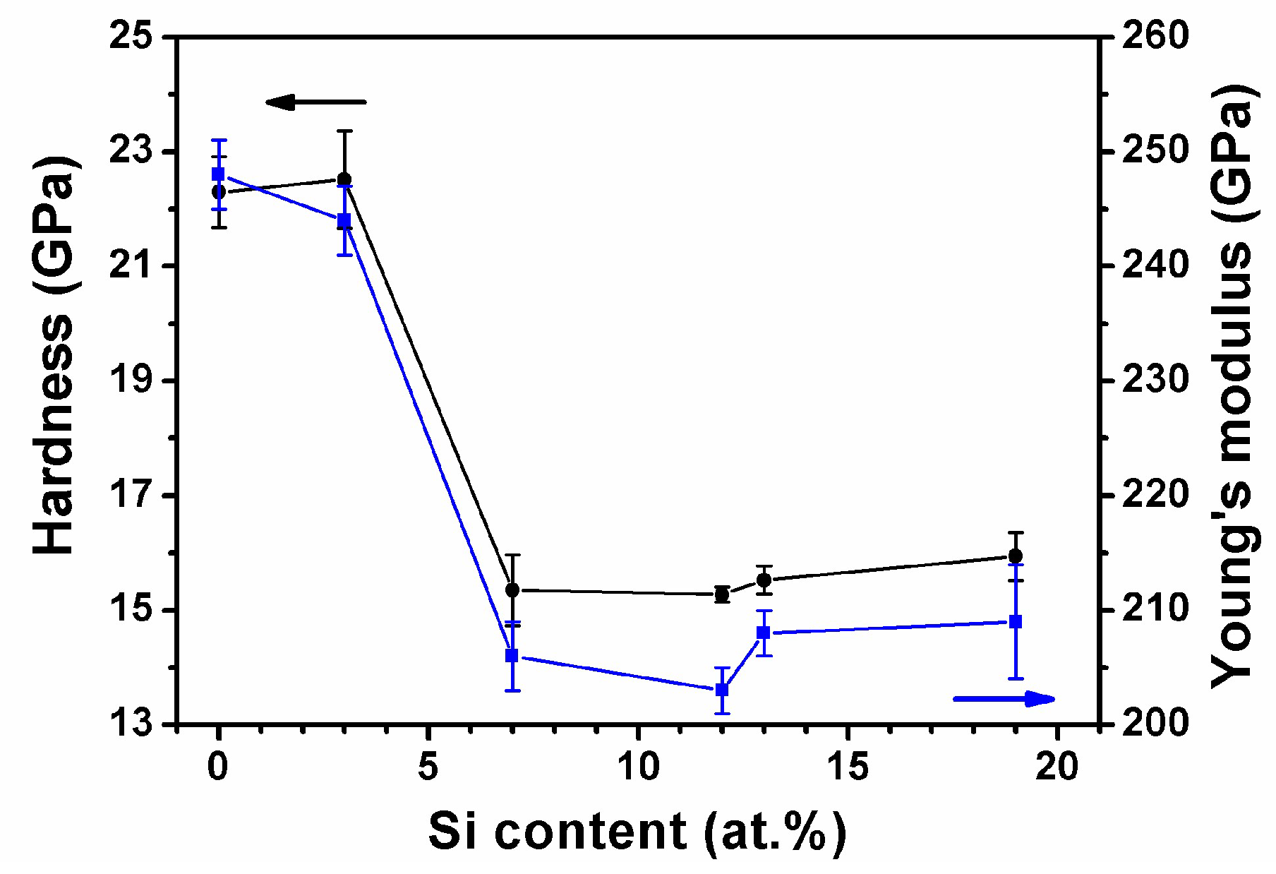
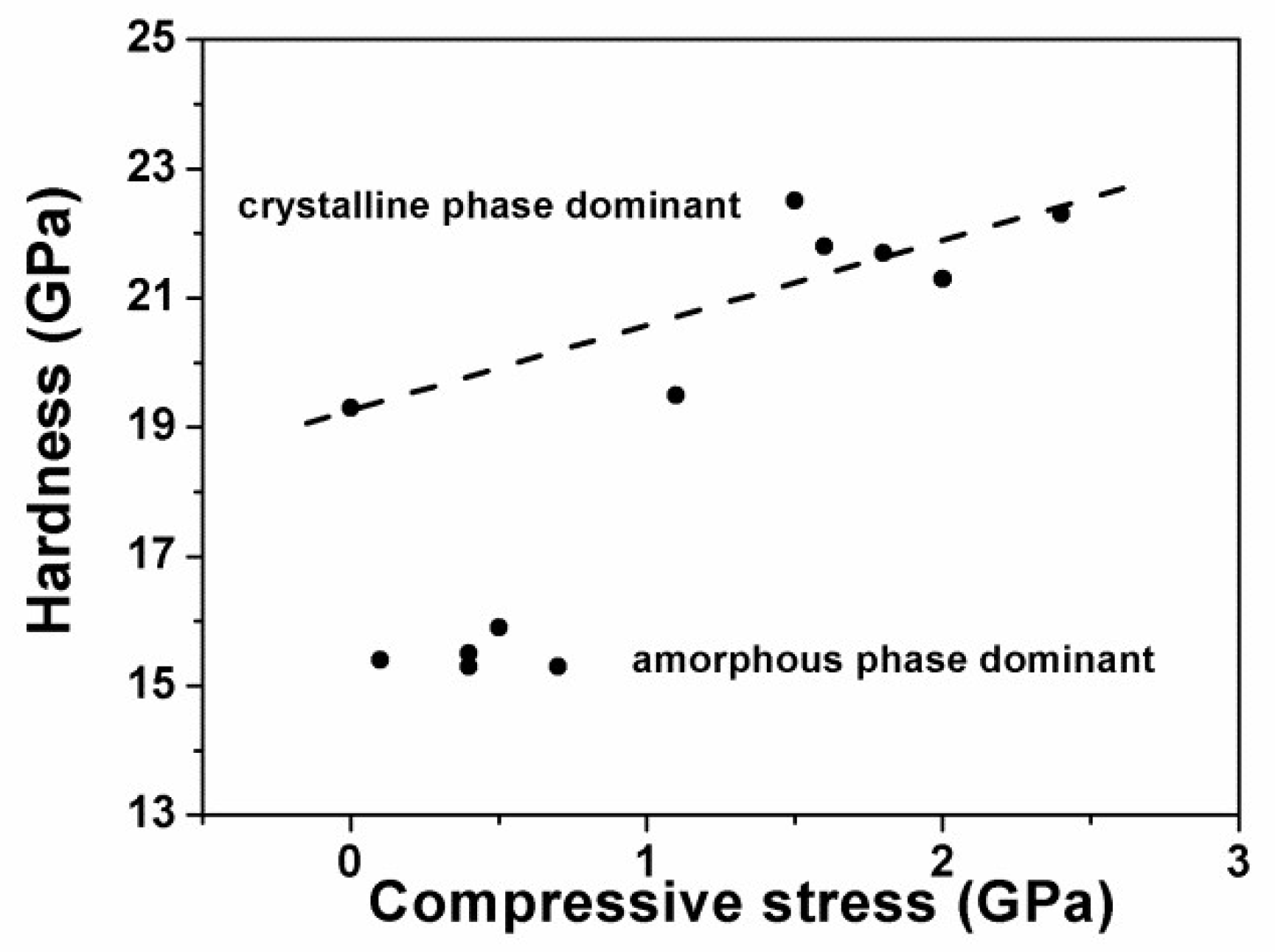
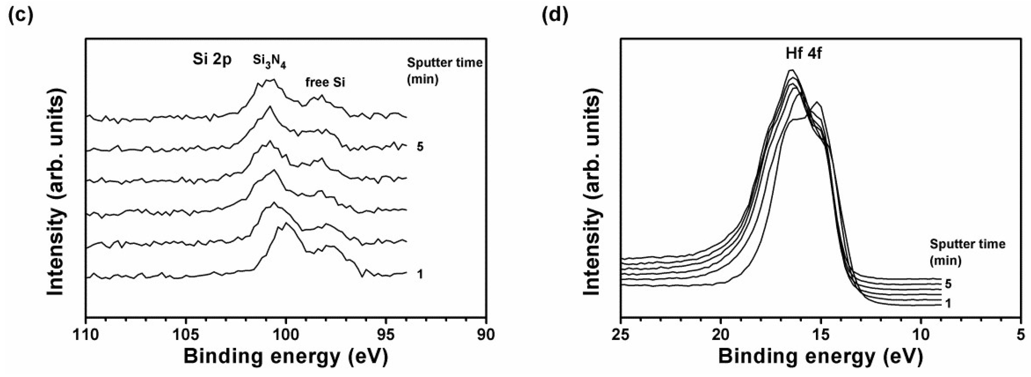
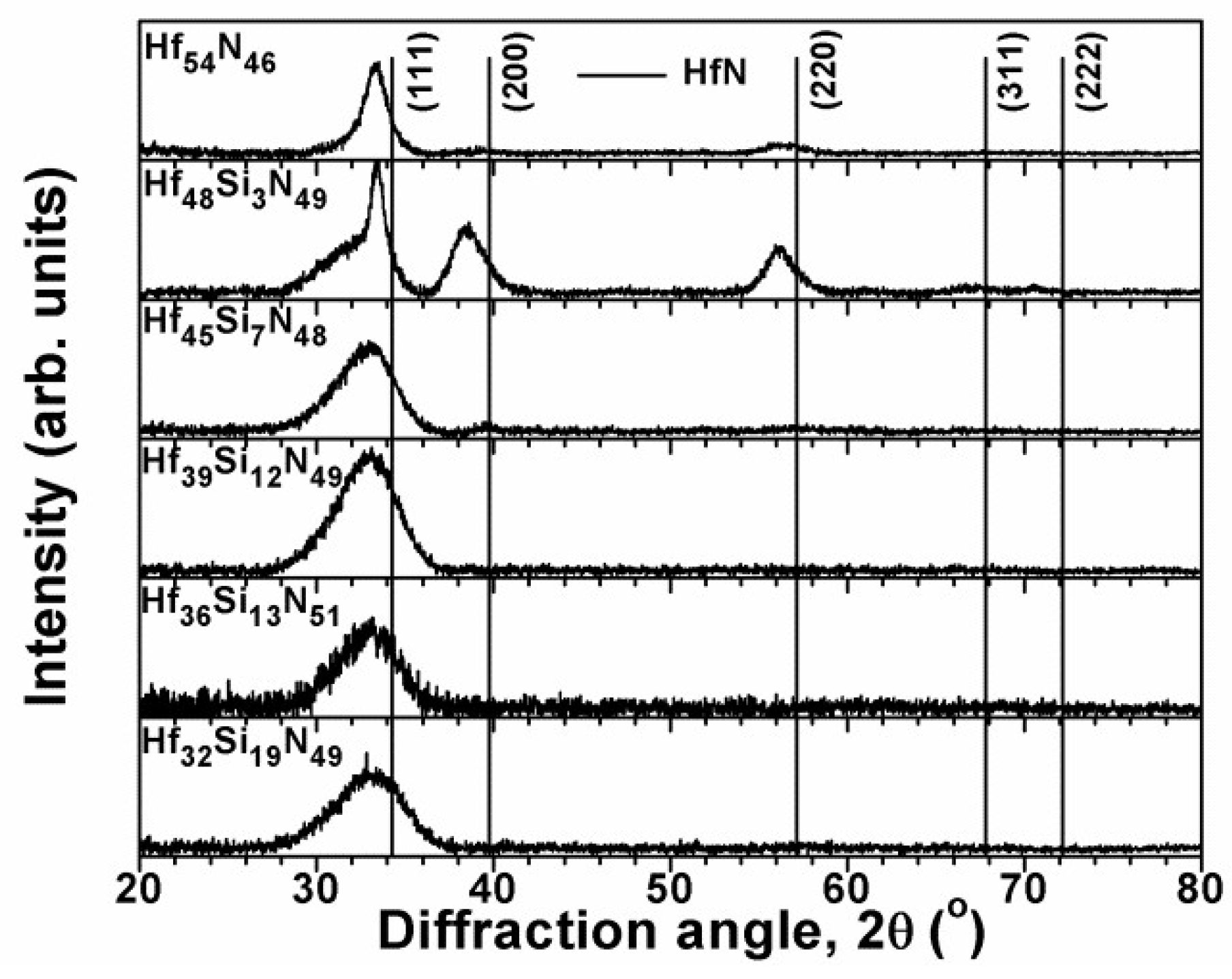
3.1.2. Multilayered Hf–Si–N Coatings
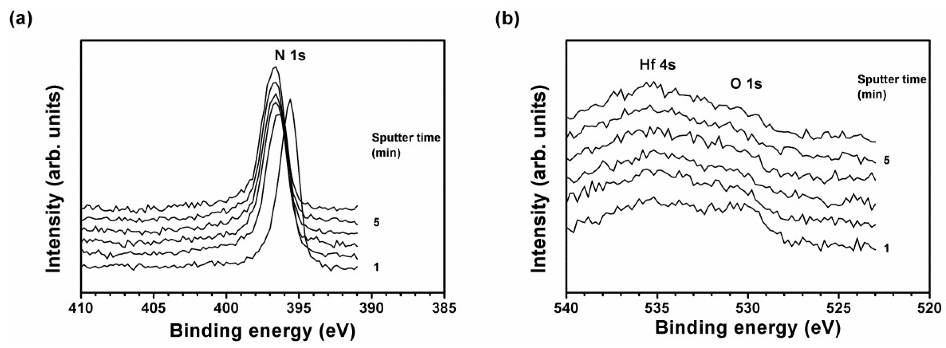
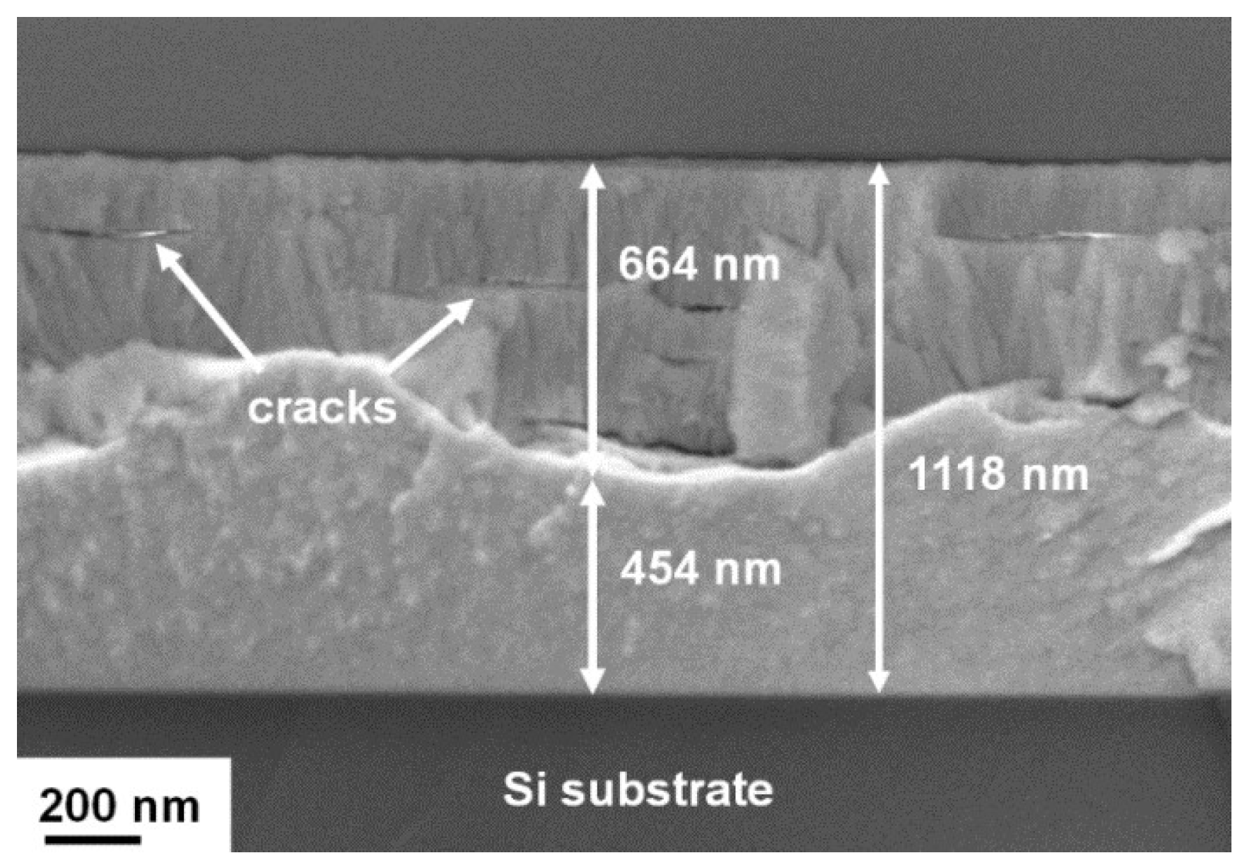
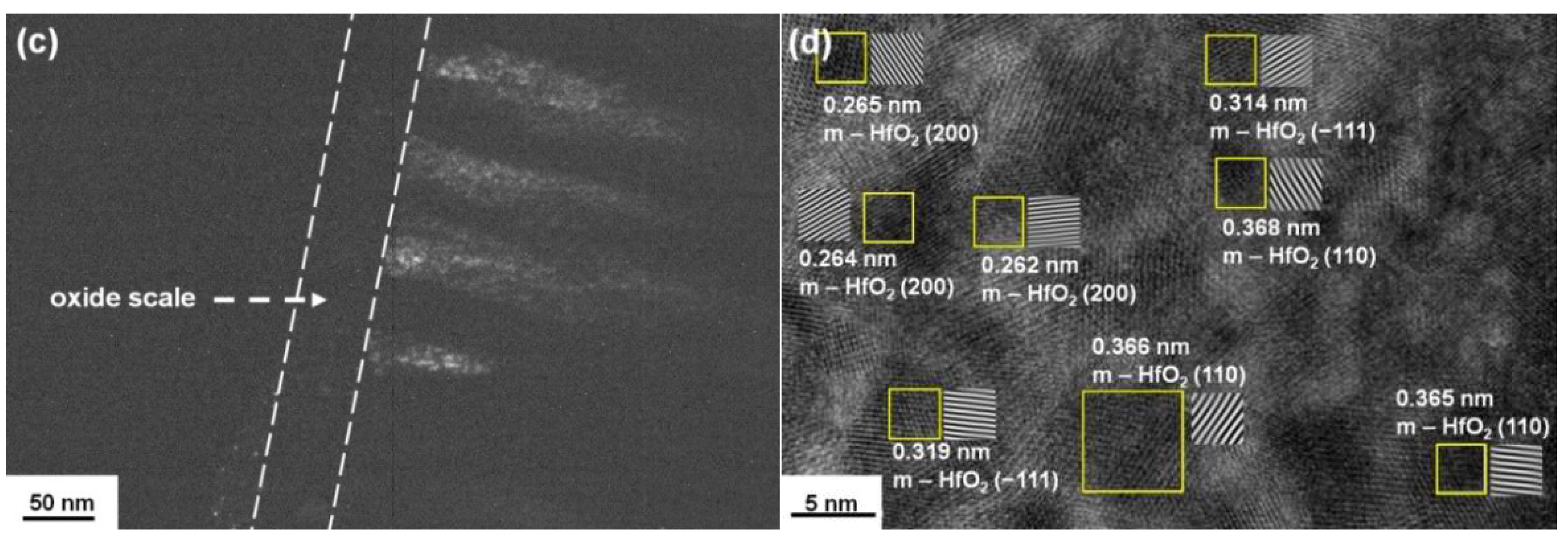
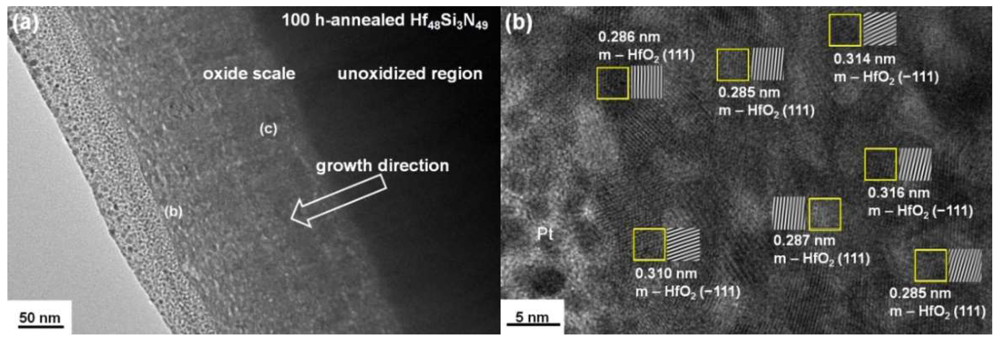
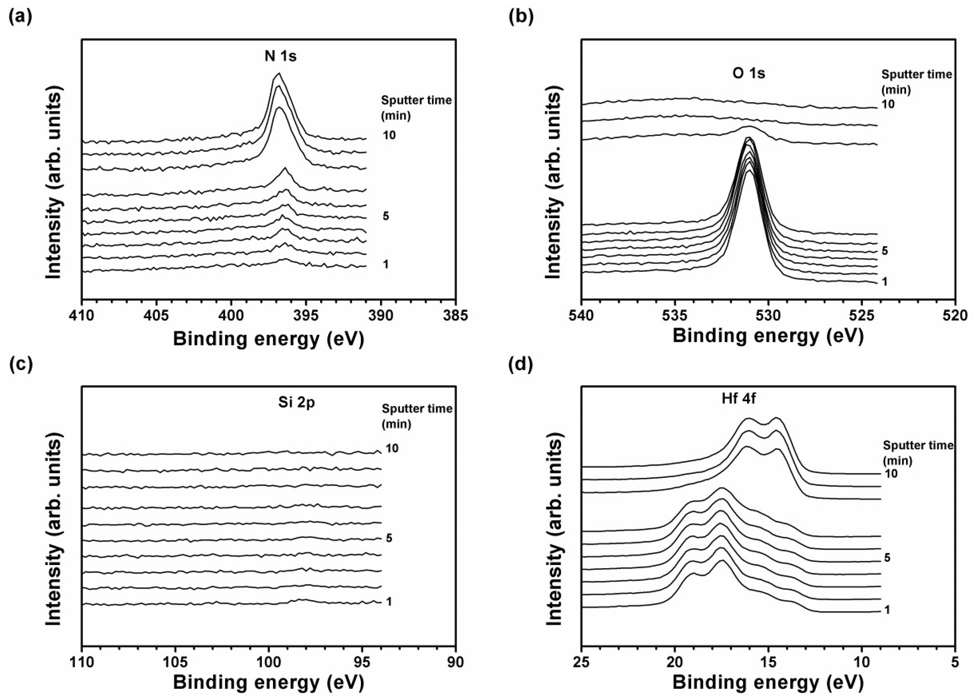
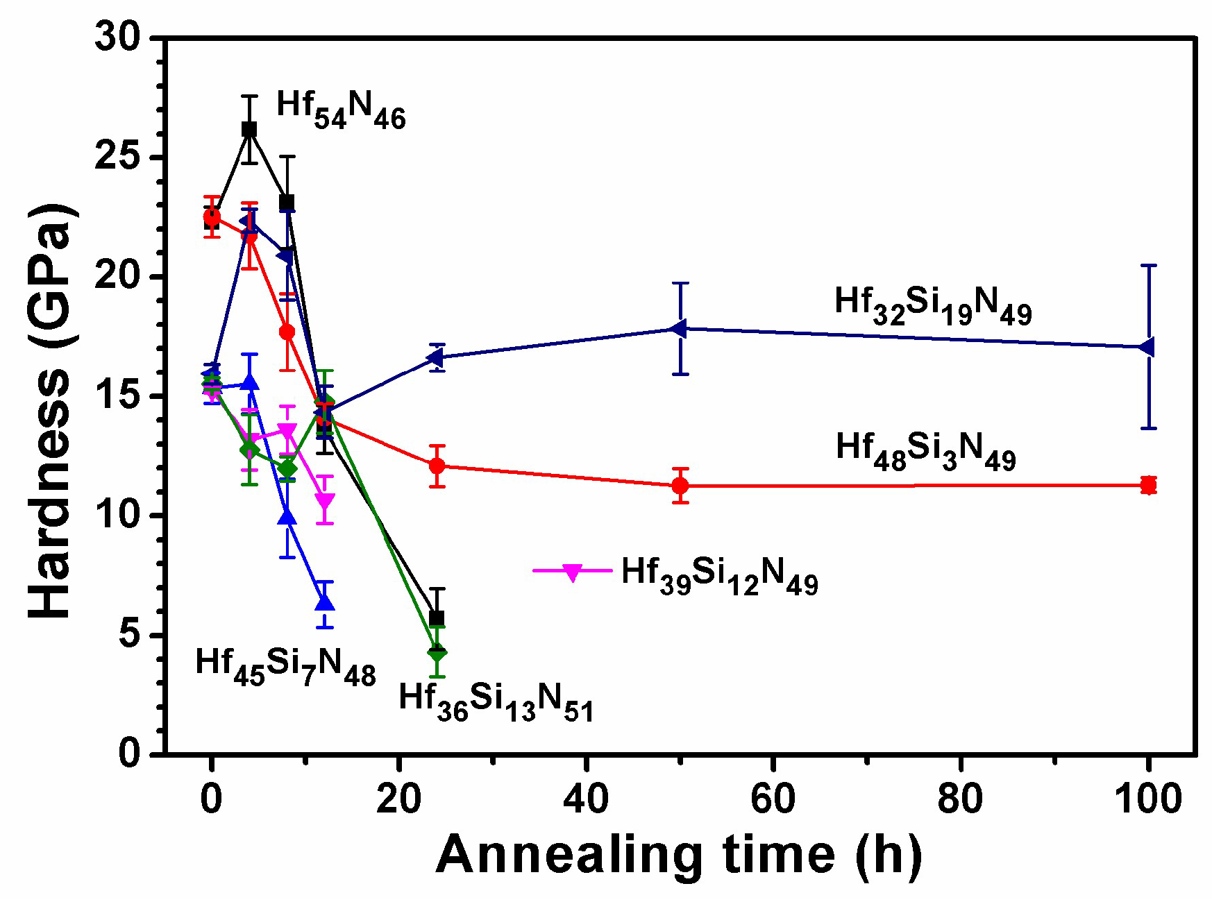
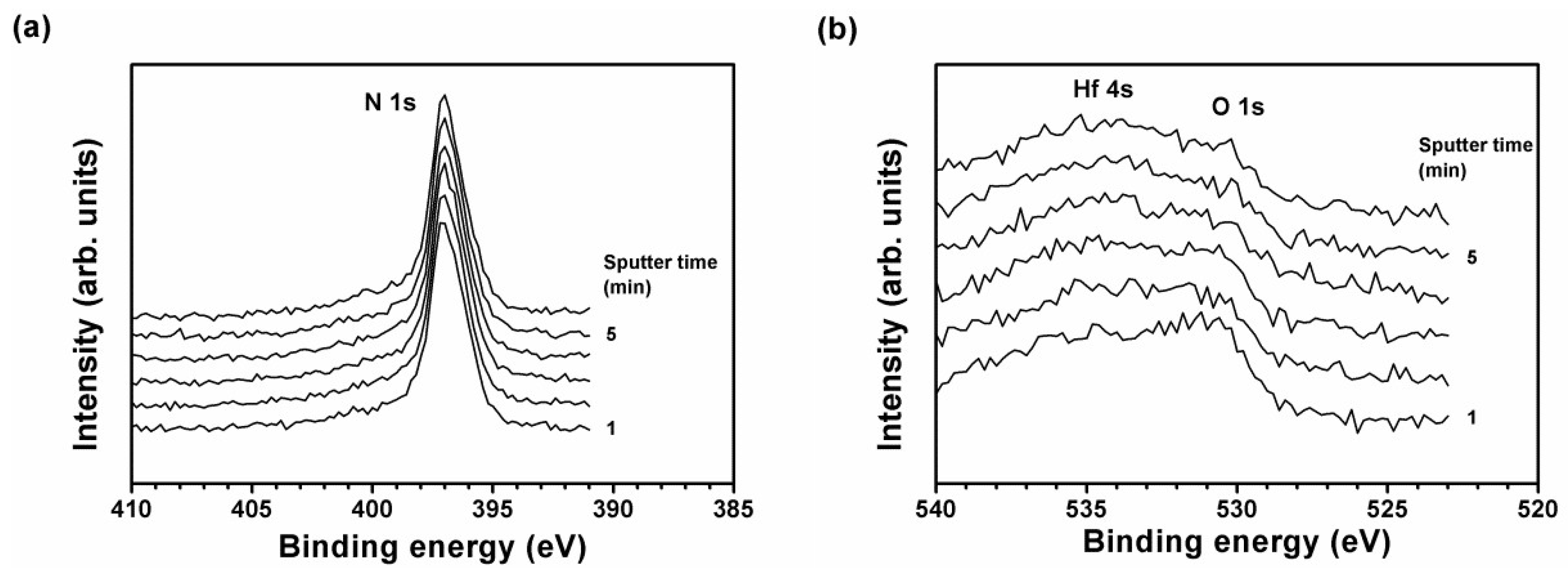
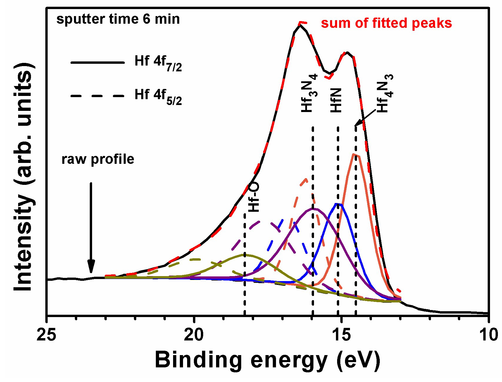
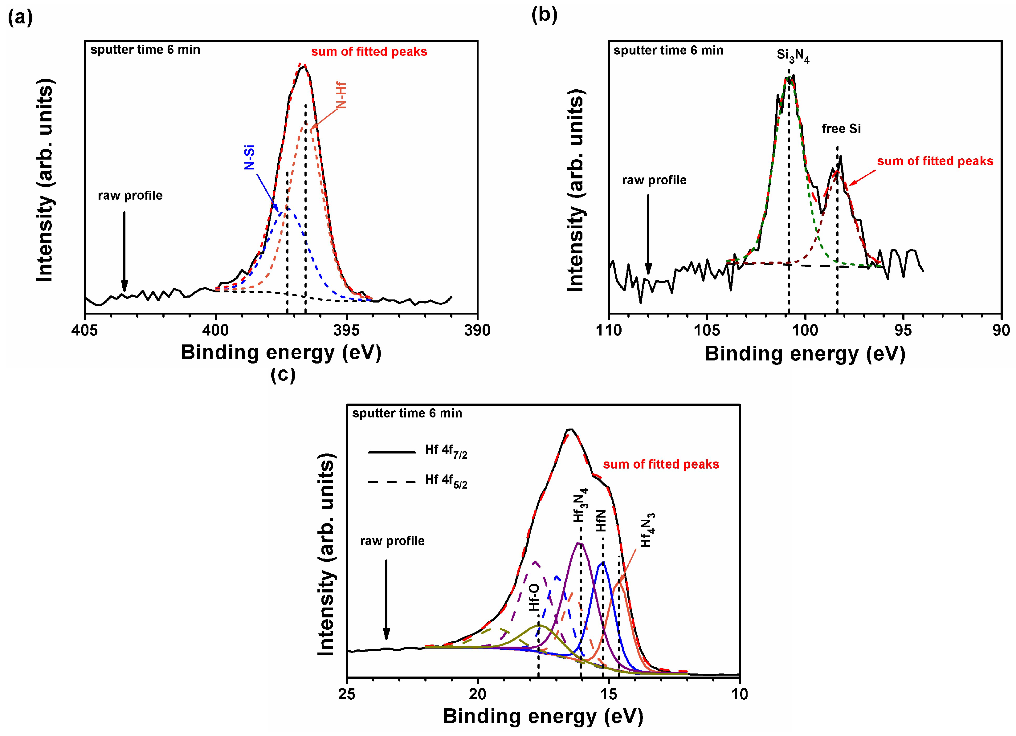
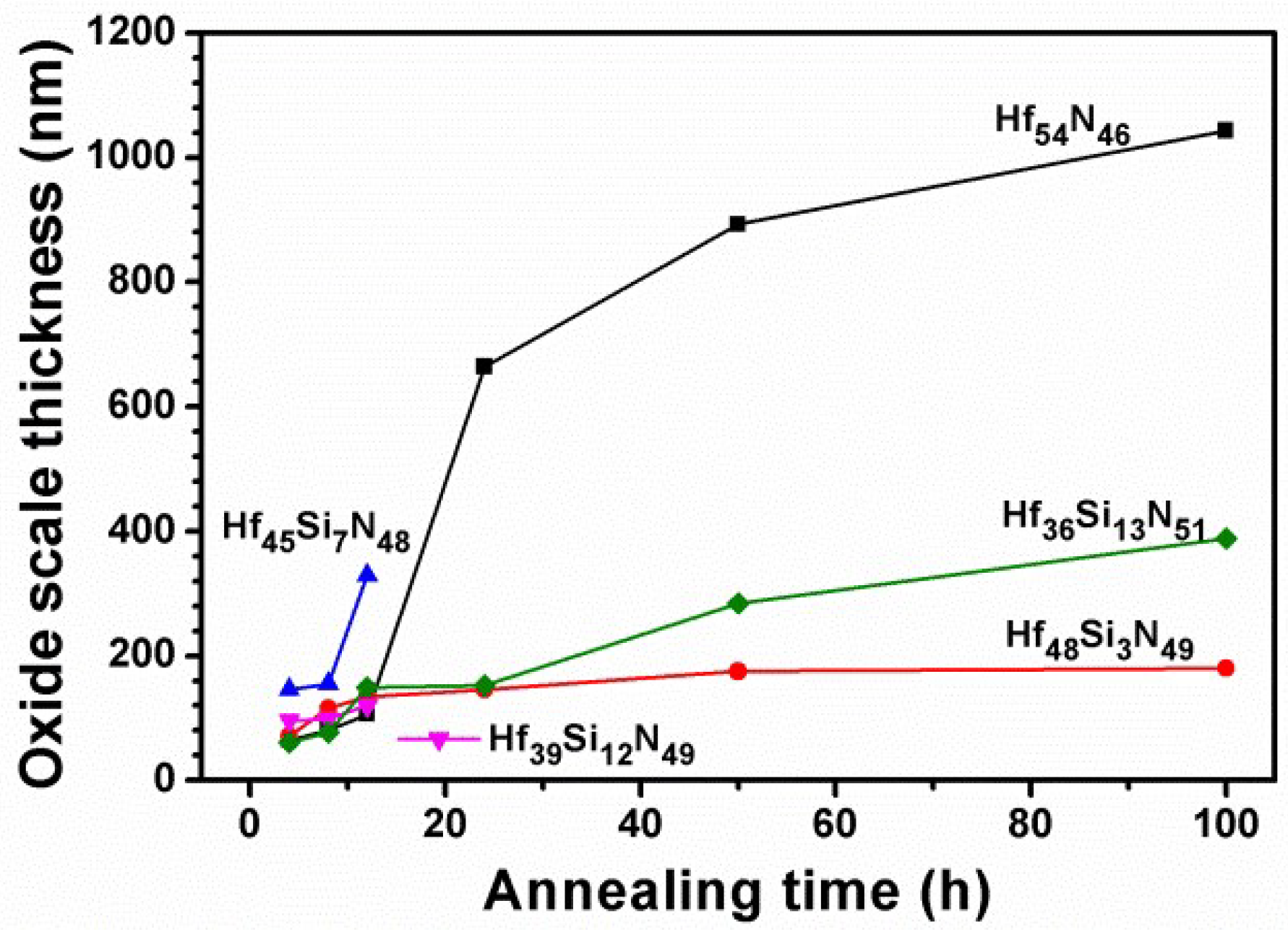
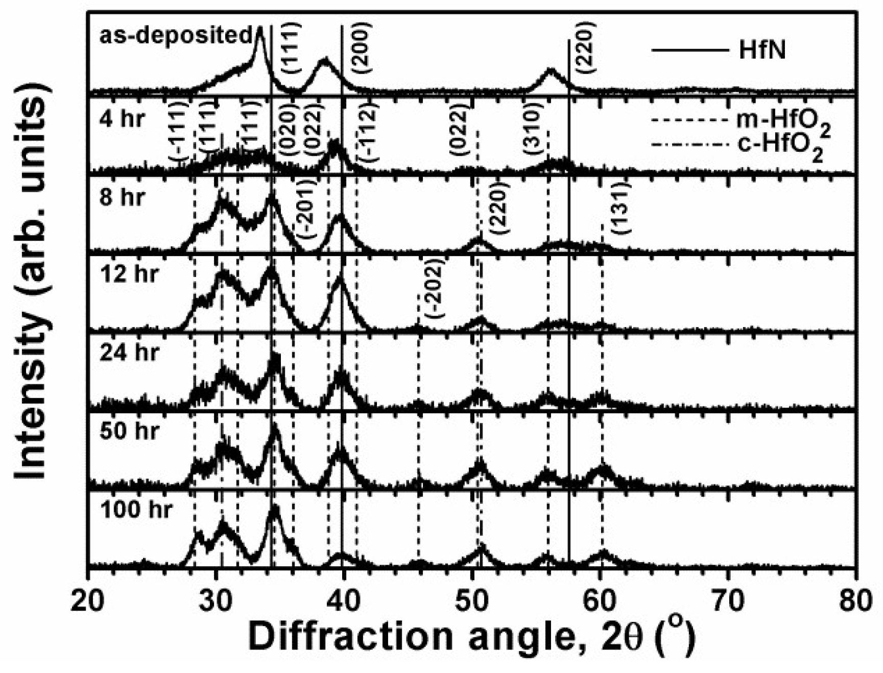
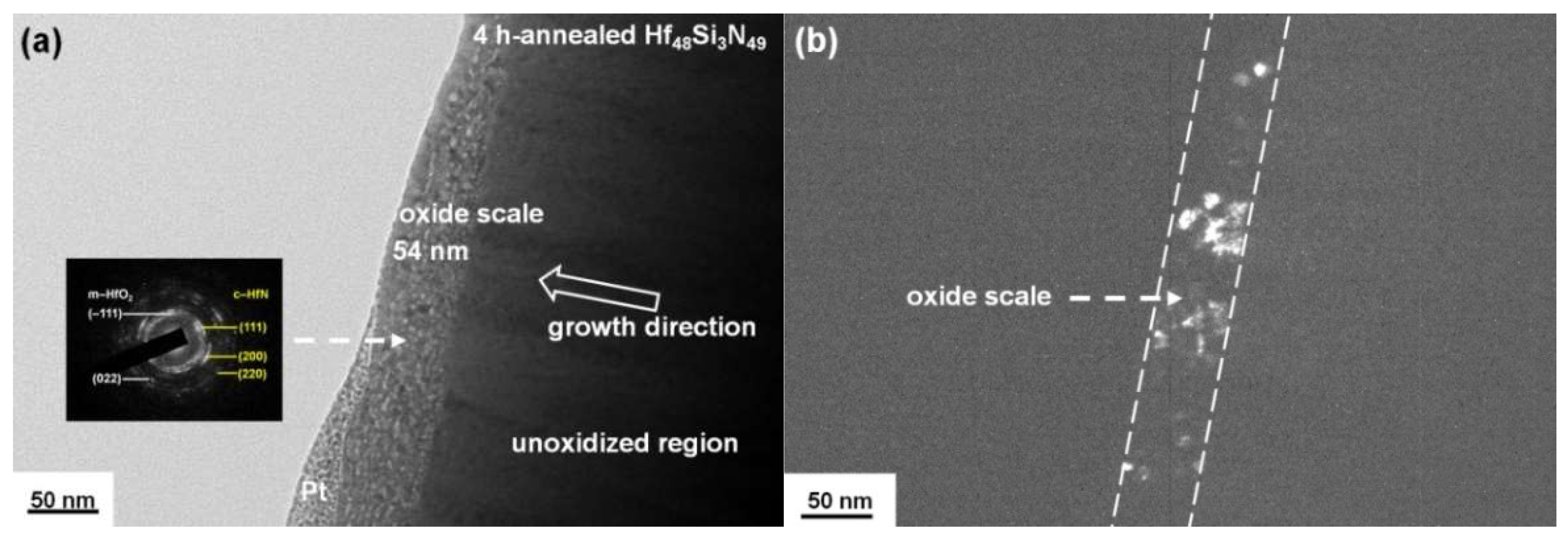
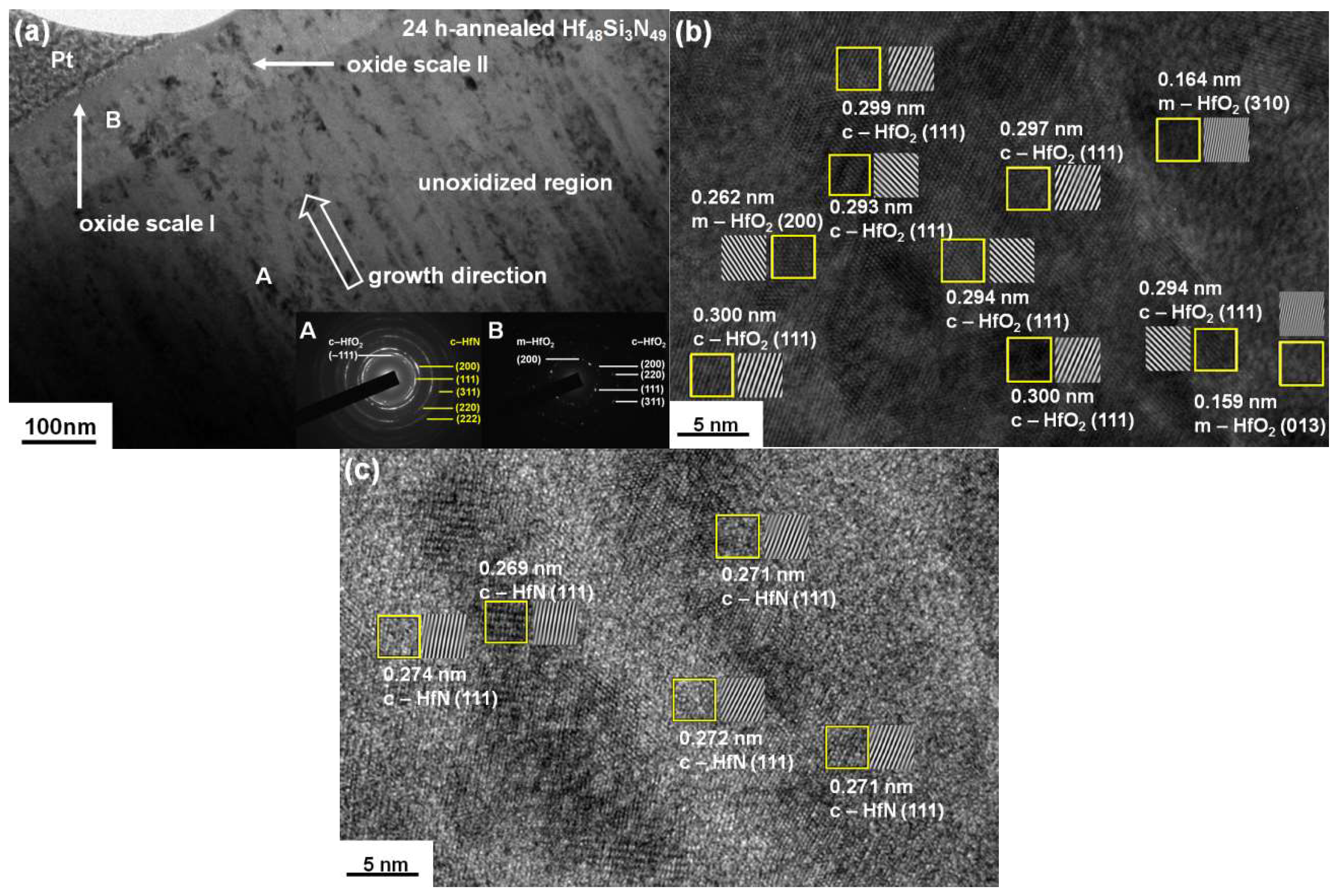
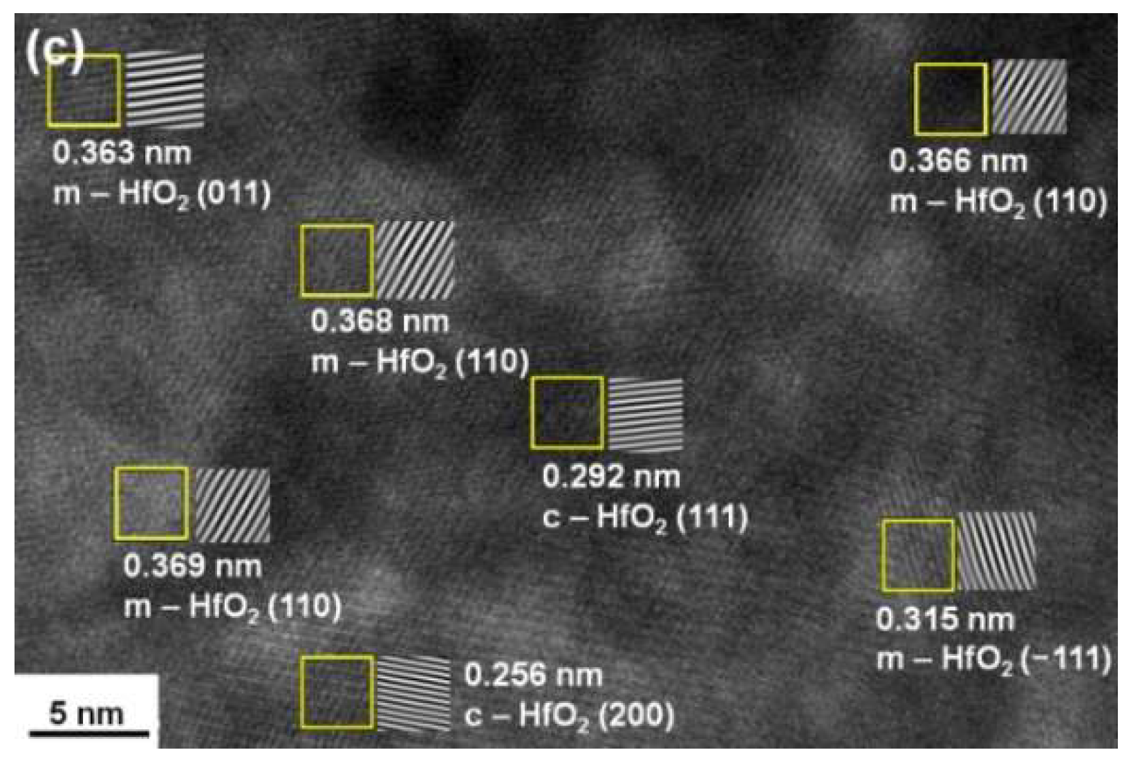
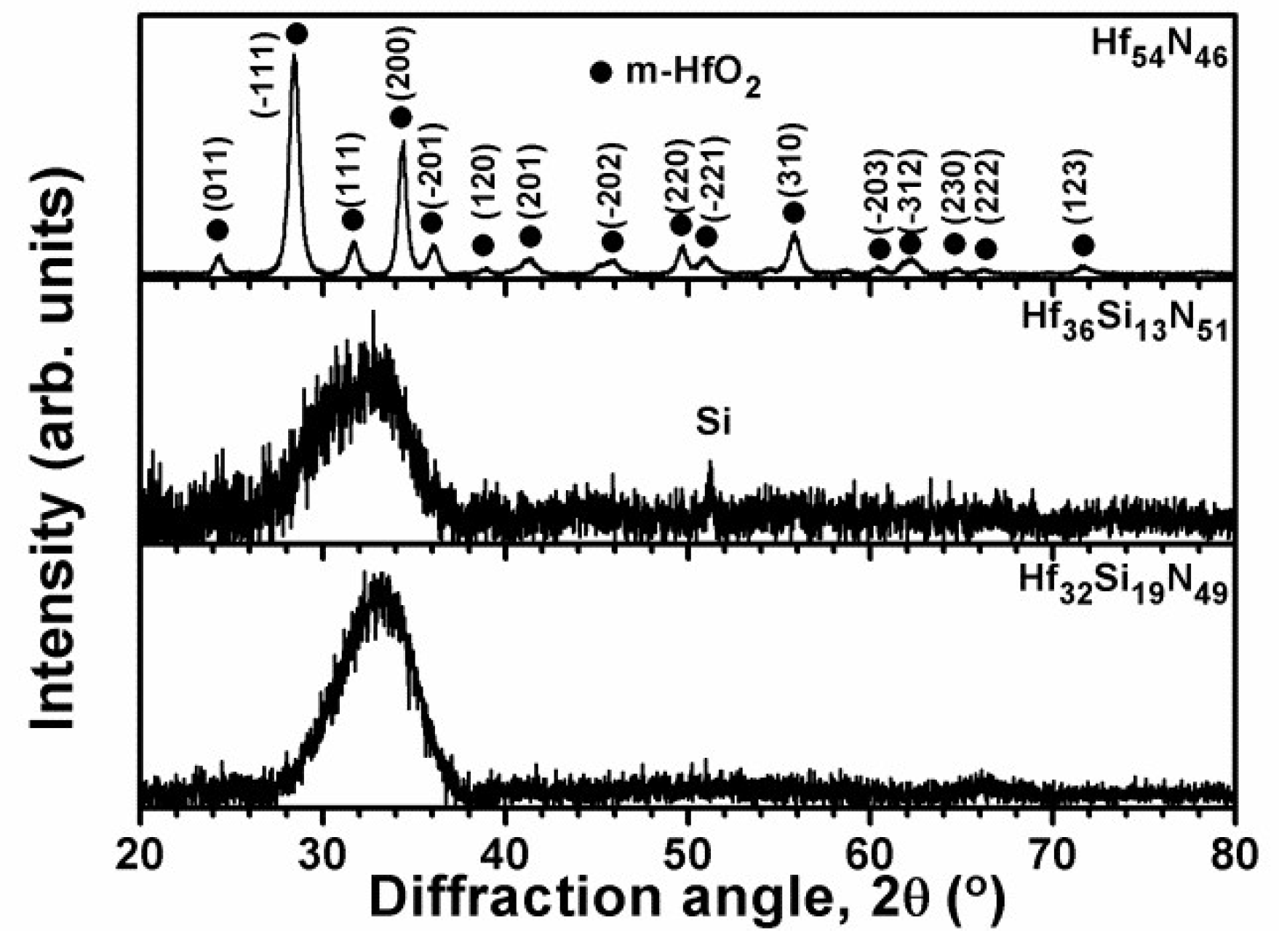
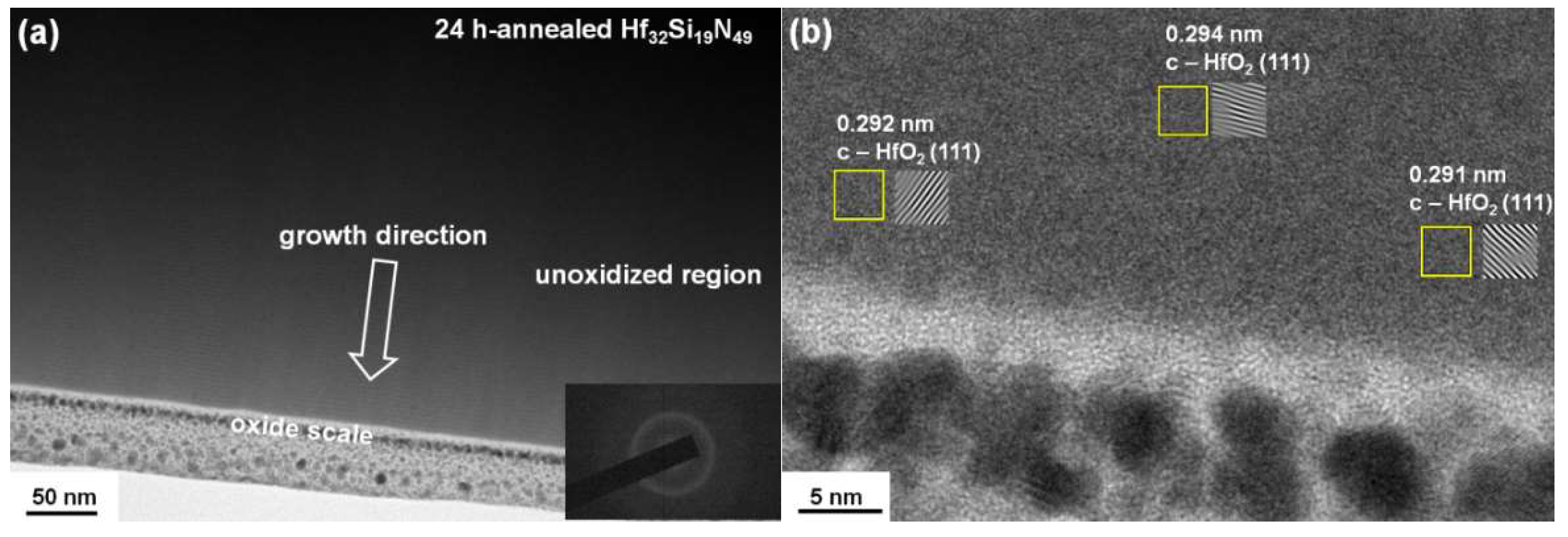
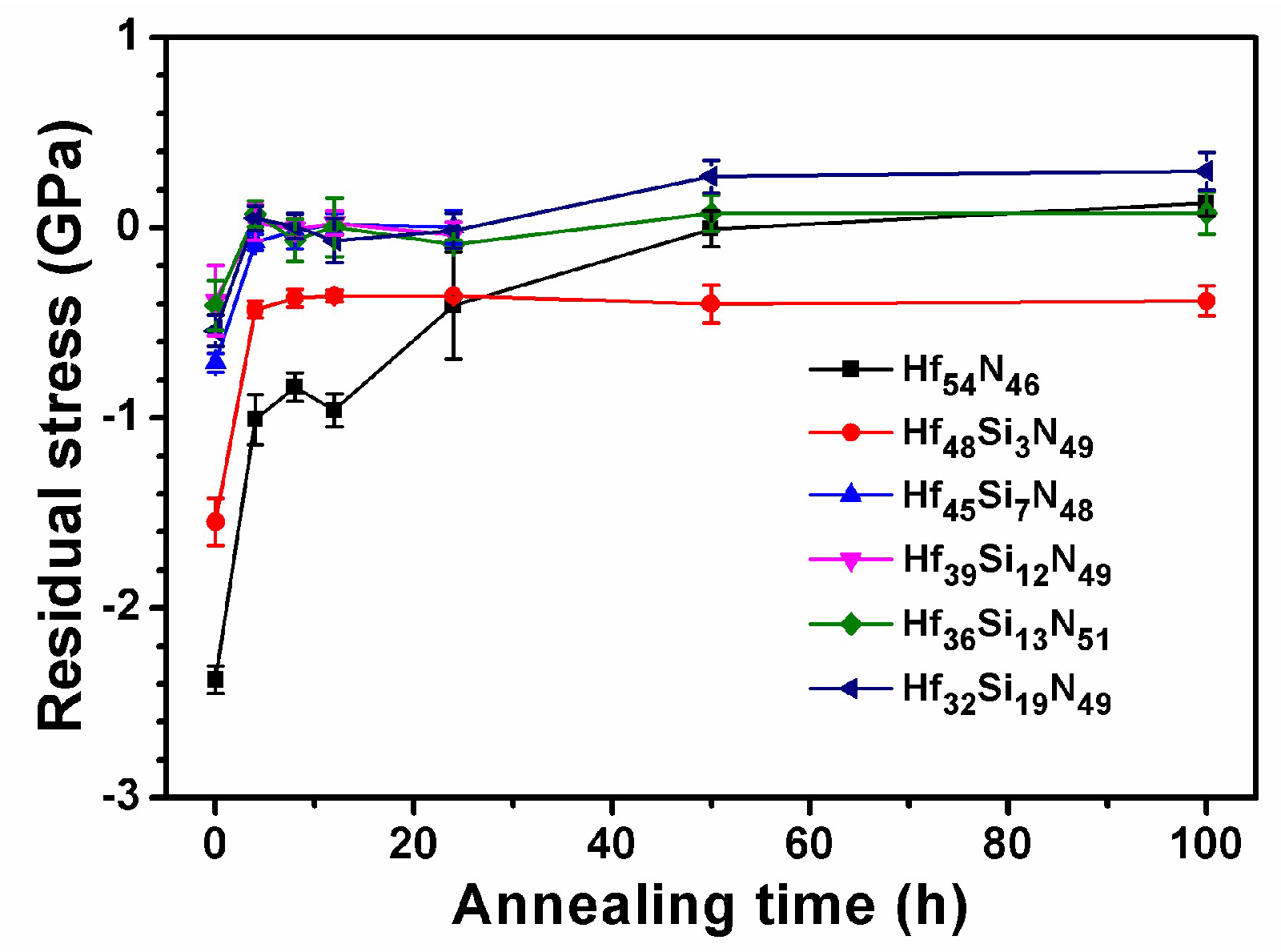
3.2. Annealed Hf–Si–N Coatings
4. Conclusions
Author Contributions
Funding
Acknowledgments
Conflicts of Interest
References
- Shin, C.-S.; Gall, D.; Hellgren, N.; Patscheider, J.; Petrov, I.; Greene, J.E. Vacancy hardening in single-crystal TiNx(001) layers. J. Appl. Phys. 2003, 93, 6025–6028. [Google Scholar] [CrossRef]
- Chou, W.J.; Yu, G.P.; Huang, J.H. Bias effect of ion-plated zirconium nitride film on Si(100). Thin Solid Films 2002, 405, 162–169. [Google Scholar] [CrossRef]
- Seo, H.-S.; Lee, T.-Y.; Wen, J.G.; Petrov, I.; Greene, J.E.; Gall, D. Growth and physical properties of epitaxial HfN layers on MgO(001). J. Appl. Phys. 2004, 96, 878–884. [Google Scholar] [CrossRef]
- Escobar, C.; Villarreal, M.; Caicedo, J.C.; Esteve, J.; Prieto, P. Mechanical and tribological behavior of VN and HfN films deposited via reactive magnetron sputtering. Surf. Rev. Lett. 2013, 20, 1350040. [Google Scholar] [CrossRef]
- Massiani, Y.; Medjahed, A.; Crousier, J.P.; Gravier, P.; Rebatel, I. Corrosion of sputtered titanium nitride films deposited on iron and stainless steel. Surf. Coat. Technol. 1991, 45, 115–120. [Google Scholar] [CrossRef]
- Chou, W.J.; Yu, G.P.; Huang, J.H. Corrosion resistance of ZrN films on AISI 304 stainless steel substrate. Surf. Coat. Technol. 2003, 167, 59–67. [Google Scholar] [CrossRef]
- Escobar, C.; Villarreal, M.; Caicedo, J.C.; Aperador, W.; Prieto, P. Novel performance in physical and corrosion resistance HfN/VN coating system. Surf. Coat. Technol. 2013, 221, 182–190. [Google Scholar] [CrossRef]
- Budke, E.; Krempel-Hesse, J.; Maidhof, H.; Schüssler, H. Decorative hard coatings with improved corrosion resistance. Surf. Coat. Technol. 1999, 112, 108–113. [Google Scholar] [CrossRef]
- Wittmer, M.; Noser, J.; Melchior, H. Oxidation kinetics of TiN thin films. J. Appl. Phys. 1981, 52, 6659–6664. [Google Scholar] [CrossRef]
- Münz, W.D. Titanium aluminum nitride films: A new alternative to TiN coatings. J. Vac. Sci. Technol. A 1986, 4, 2717–2725. [Google Scholar] [CrossRef]
- Vepřek, S.; Haussmann, M.; Reiprich, S.; Shizhi, L.; Dian, J. Novel thermodynamically stable and oxidation resistant superhard coating materials. Surf. Coat. Technol. 1996, 86–87, 394–401. [Google Scholar] [CrossRef]
- Steyer, P.; Pilloud, D.; Pierson, J.F.; Millet, J.-P.; Charnay, M.; Stauder, B.; Jacquot, P. Oxidation resistance improvement of arc-evaporated TiN hard coatings by silicon addition. Surf. Coat. Technol. 2006, 201, 4158–4162. [Google Scholar] [CrossRef]
- Pilloud, D.; Pierson, J.F.; Marco de Lucas, M.C.; Alnot, M. Stabilisation of tetragonal zirconia in oxidized Zr–Si–N nanocomposite coatings. Appl. Surf. Sci. 2004, 229, 132–139. [Google Scholar] [CrossRef]
- Zeman, P.; Musil, J. Difference in high-temperature oxidation resistance of amorphous Zr–Si–N and W–Si–N films with a high Si content. Appl. Surf. Sci. 2006, 252, 8319–8325. [Google Scholar] [CrossRef]
- Callegari, A.C.; Frank, M.M.; Jammy, R.; Lacey, D.L.; McFeely, F.R.; Zafar, S. Method of Forming HfSiN Metal for n-FET Applications. U.S. Patent 7521346, 21 April 2009. [Google Scholar]
- Miyamoto, K.; Furumai, K.; Urban, B.E.; Kondo, H.; Zaima, S. Nitrogen-content dependence of crystalline structures and resistivity of Hf–Si–N gate electrodes for metal–oxide–semiconductor field-effect transistors. Jpn. J. Appl. Phys. 2009, 48, 045505. [Google Scholar] [CrossRef]
- Jin, G.; Cui, X.; Hao, J.; Liu, E.; Wei, S.; Shao, T. Structure and corrosion resistance in physiological solution of Hf–Si–N films deposited by IBAD. Surf. Coat. Technol. 2013, 228, S449–S451. [Google Scholar] [CrossRef]
- Cui, X.; Hao, J.; Wang, Y.; Dong, M.; Jin, G. The effect of Si content on the performance of magnetron sputtering Hf–Si–N films. Phys. Procedia 2013, 50, 427–432. [Google Scholar] [CrossRef]
- Chen, Y.I.; Chang, S.C.; Chang, L.C. Oxidation resistance and mechanical properties of Zr–Si–N coatings with cyclic gradient concentration. Surf. Coat. Technol. 2017, 320, 168–173. [Google Scholar] [CrossRef]
- Musil, J. Hard nanocomposite coatings: Thermal stability, oxidation resistance and toughness. Surf. Coat. Technol. 2012, 207, 50–65. [Google Scholar] [CrossRef]
- Chen, Y.I.; Lin, K.Y.; Wang, H.H.; Cheng, Y.R. Characterization of Ta–Si–N coatings prepared using direct current magnetron co-sputtering. Appl. Surf. Sci. 2014, 305, 805–816. [Google Scholar] [CrossRef]
- Oliver, W.C.; Pharr, G.M. An improved technique for determining hardness and elastic modulus using load and displacement sensing indentation experiments. J. Mater. Res. 1992, 7, 1564–1583. [Google Scholar] [CrossRef]
- Janssen, G.C.A.M.; Abdalla, M.M.; van Keulen, F.; Pujada, B.R.; van Venrooy, B. Celebrating the 100th anniversary of the Stoney equation for film stress: Developments from polycrystalline steel strips to single crystal silicon wafers. Thin Solid Films 2009, 517, 1858–1867. [Google Scholar] [CrossRef]
- Brantley, W.A. Calculated elastic constants for stress problems associated with semiconductor devices. J. Appl. Phys. 1973, 44, 534–535. [Google Scholar] [CrossRef]
- Massalski, T.B. Hf–N (Hafnium–Nitrogen). In Binary Alloy Phase Diagrams, 2nd ed.; Massalski, T.B., Okamoto, H., Subramanian, P.R., Kacprzak, L., Eds.; ASM International: Materials Park, OH, USA, 1990; p. 2090. [Google Scholar]
- Johansson, B.O.; Helmersson, U.; Hibbs, M.K.; Sundgren, J.E. Reactively magnetron sputtered HfN films. I. Composition and structure. J. Appl. Phys. 1985, 58, 3104–3111. [Google Scholar] [CrossRef]
- Zerr, A.; Miehe, G.; Riedel, R. Synthesis of cubic zirconium and hafnium nitride having Th3P4 structure. Nat. Mater. 2003, 2, 185–189. [Google Scholar] [CrossRef] [PubMed]
- Kroll, P. Hafnium nitride with thorium phosphide structure: Physical properties and an assessment of the Hf–N, Zr–N, and Ti–N phase diagrams at high pressures and temperatures. Phys. Rev. Lett. 2003, 90, 125501. [Google Scholar] [CrossRef] [PubMed]
- Escobar, C.; Villarreal, M.; Caicedo, J.C.; Aperador, W.; Prieto, P. Mechanical properties of steel surfaces coated with HfN/VN superlattices. J. Mater. Eng. Perform. 2014, 23, 3963–3974. [Google Scholar] [CrossRef]
- García-González, L.; Zamora-Peredo, L.; Flores-Ramírez, N.; Garnica-Romo, M.G.; Hernández-Torres, J. Influence of nitrogen flow rates on the structure, hardness, and electrical resistivity of HfN coatings by DC sputtering. J. Mater. Eng. Perform. 2015, 24, 1558–1564. [Google Scholar] [CrossRef]
- Dong, Y.; Zhao, W.; Yue, J.; Li, G. Crystallization of Si3N4 layers and its influences on the microstructure and mechanical properties of ZrN/Si3N4 nanomultilayers. Appl. Phys. Lett. 2006, 89, 121916. [Google Scholar] [CrossRef]
- Abadias, G.; Uglov, V.V.; Saladukhin, I.A.; Zlotski, S.V.; Tolmachova, G.; Dub, S.N.; Janse van Vuuren, A. Growth, structural and mechanical properties of magnetron-sputtered ZrN/SiNx nanolaminated coatings. Surf. Coat. Technol. 2016, 308, 158–167. [Google Scholar] [CrossRef]
- Cardarelli, F. Materials Handbook, 2nd ed.; Springer: London, UK, 2008. [Google Scholar]
- Chen, Y.H.; Guruz, M.; Chung, Y.W.; Keer, L.M. Thermal stability of hard TiNySiNx multilayer coatings with an equiaxed microstructure. Surf. Coat. Technol. 2002, 154, 162–166. [Google Scholar] [CrossRef]
- Arranz, A. Synthesis of hafnium nitride films by 0.5–5 keV nitrogen implantation of metallic Hf: An X-ray photoelectron spectroscopy and factor analysis study. Surf. Sci. 2004, 563, 1–12. [Google Scholar] [CrossRef]
- Wang, W.; Nabatame, T.; Shimogaki, Y. Interface structure of HfNx/SiO2 stack grown by MOCVD using TDEAHf precursor. Surf. Sci. 2005, 588, 108–116. [Google Scholar] [CrossRef]
- Choi, J.B.; Cho, K.; Lee, M.H.; Kim, K.H. Effects of Si content and free Si on oxidation behavior of Ti–Si–N coating layers. Thin Solid Films 2004, 447–448, 365–370. [Google Scholar] [CrossRef]
- Chen, Y.I.; Gao, Y.X.; Chang, L.C.; Ke, Y.E.; Liu, B.W. Mechanical properties, bonding characteristics, and oxidation behaviors of Nb–Si–N coatings. Surf. Coat. Technol. 2018, 350, 831–840. [Google Scholar] [CrossRef]
- Chang, L.-C.; Zheng, Y.-Z.; Chen, Y.-I.; Chang, S.-C.; Liu, B.-W. Bonding characteristics and chemical inertness of Zr–Si–N coatings with a high Si content in glass molding. Coatings 2018, 8, 181. [Google Scholar] [CrossRef]
- Xu, M.; Wang, S.; Yin, G.; Li, J.; Zheng, Y.; Chen, L.; Jia, Y. Optical properties of cubic Ti3N4, Zr3N4, and Hf3N4. Appl. Phys. Lett. 2006, 89, 151908. [Google Scholar] [CrossRef]
- Barin, I. Thermochemical Data of Pure Substances, 3rd ed.; Wiley-VCH Verlag GmbH & Co. KGaA: New York, NY, USA, 1995. [Google Scholar]
- Okutomi, M.; Kasamatsu, M.; Tsukamoto, K.; Shiratori, S.; Uchiyama, F. Sintering of new oxide ceramics using a high power cw CO2 laser. Appl. Phys. Lett. 1984, 44, 1132–1134. [Google Scholar] [CrossRef]
- Tapily, K.; Jakes, J.E.; Stone, D.S.; Shrestha, P.; Gu, D.; Baumgart, H.; Elmustafa, A.A. Nanoindentation investigation of HfO2 and Al2O3 films grown by atomic layer deposition. J. Electrochem. Soc. 2008, 155, H545–H551. [Google Scholar] [CrossRef]
- Al-Khatatbeh, Y.; Lee, K.K.M.; Kiefer, B. Phase diagram up to 105 GPa and mechanical strength of HfO2. Phys. Rev. B 2010, 82, 144106. [Google Scholar] [CrossRef]


| Position | Sample | Chemical Composition (at.%) | T (nm) | H (GPa) | E (GPa) | Stress (GPa) | |||
|---|---|---|---|---|---|---|---|---|---|
| Hf | Si | N | O | ||||||
| 1 | Hf45Si6N49 | 44.5 ± 0.9 | 5.5 ± 0.1 | 49.0 ± 1.6 | 1.0 ± 0.1 | 1009 | 19.5 ± 0.4 | 256 ± 7 | −1.1 ± 0.2 |
| 2 | Hf49Si1N50 | 48.3 ± 1.8 | 1.2 ± 0.1 | 49.6 ± 2.1 | 0.9 ± 0.4 | 1559 | 21.7 ± 1.1 | 284 ± 6 | −1.8 ± 0.2 |
| 3 | Hf53Si1N46 | 52.1 ± 0.8 | 1.3 ± 0.1 | 45.5 ± 0.8 | 1.1 ± 0.3 | 1122 | 21.3 ± 1.4 | 283 ± 9 | −2.0 ± 0.0 |
| 4 | Hf50Si3N47 | 50.0 ± 1.4 | 2.8 ± 0.1 | 45.9 ± 1.2 | 1.3 ± 0.3 | 667 | 21.8 ± 1.3 | 264 ± 8 | −1.6 ± 0.8 |
| 5 | Hf44Si7N49 | 43.4 ± 0.3 | 6.6 ± 0.1 | 48.1 ± 0.7 | 1.9 ± 0.5 | 628 | 19.3 ± 2.2 | 246 ± 16 | 0.0 ± 0.6 |
| 6 | Hf38Si12N50 | 38.1 ± 0.8 | 11.9 ± 0.2 | 49.4 ± 0.5 | 0.6 ± 0.2 | 649 | 15.4 ± 1.1 | 227 ± 10 | −0.1 ± 0.2 |
| Sample | Power (W) | Time (min) | Chemical Composition (at.%) | Thickness (nm) | Hardness (GPa) | Young’s Modulus (GPa) | Stress (GPa) | ||||
|---|---|---|---|---|---|---|---|---|---|---|---|
| Hf | Si | Hf | Si | N | O | ||||||
| Hf54N46 | 250 | 0 | 90 | 52.2 ± 4.0 | 0.2 ± 0.1 | 44.4 ± 4.5 | 3.2 ± 0.4 | 957 | 22.3 ± 0.6 | 248 ± 3 | −2.4 ± 0.1 |
| Hf48Si3N49 | 250 | 25 | 85 | 47.2 ± 0.7 | 3.1 ± 0.1 | 47.8 ± 0.3 | 1.9 ± 0.6 | 866 | 22.5 ± 0.8 | 244 ± 3 | −1.5 ± 0.1 |
| Hf45Si7N48 | 250 | 50 | 80 | 44.7 ± 0.5 | 7.0 ± 0.2 | 47.1 ± 0.1 | 1.2 ± 0.2 | 1018 | 15.3 ± 0.6 | 206 ± 3 | −0.7 ± 0.0 |
| Hf39Si12N49 | 250 | 75 | 75 | 39.0 ± 0.8 | 11.4 ± 0.4 | 48.5 ± 1.4 | 1.1 ± 0.3 | 961 | 15.3 ± 0.1 | 203 ± 2 | −0.4 ± 0.2 |
| Hf36Si13N51 | 250 | 100 | 70 | 35.4 ± 1.0 | 13.4 ± 0.1 | 50.3 ± 1.2 | 0.9 ± 0.2 | 985 | 15.5 ± 0.2 | 208 ± 2 | −0.4 ± 0.1 |
| Hf32Si19N49 | 250 | 150 | 60 | 31.8 ± 0.4 | 18.5 ± 0.5 | 48.7 ± 1.0 | 1.0 ± 0.2 | 990 | 15.9 ± 0.4 | 209 ± 5 | −0.5 ± 0.1 |
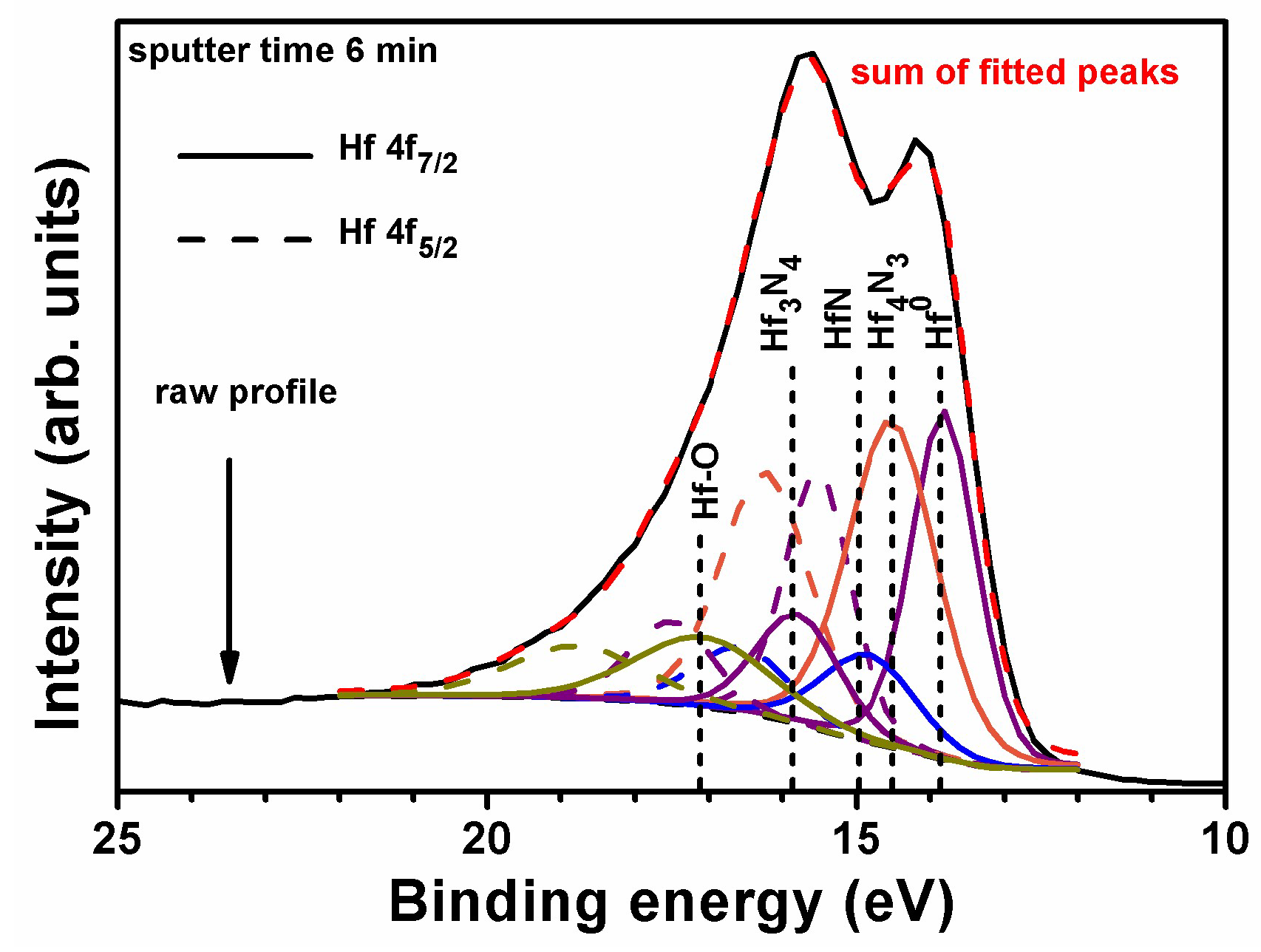
| Sample | Depth Range (nm) | Hf 4f7/2 (eV) | Intensity Ratio of Hf0:Hf4N3:HfN:Hf3N4:Hf–O | ||||
|---|---|---|---|---|---|---|---|
| Hf0 | Hf4N3 | HfN | Hf3N4 | Hf–O | |||
| Hf48Si3N49 | |||||||
| as-deposited | 9.5–57.0 | – | 14.46 ± 0.06 | 15.13 ± 0.03 | 16.01 ± 0.07 | 18.11 ± 0.09 | 0:31:24:34:11 |
| annealed, 24 h | 205–256, unoxidized | 13.84 ± 0.02 | 14.48 ± 0.01 | 15.02 ± 0.02 | 16.01 ± 0.00 | 17.50 ± 0.07 | 18:29:34:12:7 |
| 26–179, oxidized | 13.85 ± 0.02 | 14.48 ± 0.03 | 14.98 ± 0.01 | 16.07 ± 0.04 | 17.51 ± 0.02 | 11:2:5:30:52 | |
| Hf45Si7N48 | |||||||
| as-deposited | 9.5–57.0 | 13.82 ± 0.03 | 14.53 ± 0.01 | 14.82 ± 0.03 | 15.82 ± 0.03 | 17.06 ± 0.08 | 28:36:11:12:13 |
| annealed, 8 h | 161–230, unoxidized | 13.86 ± 0.01 | 14.50 ± 0.02 | 15.00 ± 0.28 | 15.72 ± 0.09 | 16.90 ± 0.03 | 23:39:10:16:12 |
| 23–115, oxidized | 13.50 ± 0.02 | 14.84 ± 0.08 | 15.09 ± 0.07 | 16.21 ± 0.04 | 16.97 ± 0.02 | 5:9:15:10:61 | |
| Hf32Si19N49 | |||||||
| as-deposited | 28.5–57.0 | – | 14.60 ± 0.02 | 15.25 ± 0.01 | 16.07 ± 0.03 | 17.53 ± 0.06 | 0:23:26:40:11 |
| annealed, 24 h | 16.8–33.6, unoxidized | 13.92 ± 0.02 | 14.53 ± 0.03 | 15.18 ± 0.02 | 15.70 ± 0.03 | 16.98 ± 0.05 | 18:29:30:16:7 |
| 8.4, oxidized | – | – | – | 16.00 | 16.78 | 0:0:0:20:80 | |
© 2018 by the authors. Licensee MDPI, Basel, Switzerland. This article is an open access article distributed under the terms and conditions of the Creative Commons Attribution (CC BY) license (http://creativecommons.org/licenses/by/4.0/).
Share and Cite
Chang, L.-C.; Liu, B.-W.; Chen, Y.-I. Mechanical Properties and Oxidation Behavior of Multilayered Hf–Si–N Coatings. Coatings 2018, 8, 354. https://doi.org/10.3390/coatings8100354
Chang L-C, Liu B-W, Chen Y-I. Mechanical Properties and Oxidation Behavior of Multilayered Hf–Si–N Coatings. Coatings. 2018; 8(10):354. https://doi.org/10.3390/coatings8100354
Chicago/Turabian StyleChang, Li-Chun, Bo-Wei Liu, and Yung-I Chen. 2018. "Mechanical Properties and Oxidation Behavior of Multilayered Hf–Si–N Coatings" Coatings 8, no. 10: 354. https://doi.org/10.3390/coatings8100354
APA StyleChang, L.-C., Liu, B.-W., & Chen, Y.-I. (2018). Mechanical Properties and Oxidation Behavior of Multilayered Hf–Si–N Coatings. Coatings, 8(10), 354. https://doi.org/10.3390/coatings8100354