Review

Thermal Growth of Graphene: A Review

1
College of Mechanical and Transportation Engineering, China University of Petroleum, Beijing 102249, China
2
Beijing Key Laboratory of Fluid Filtration and Separation, China University of Petroleum, Beijing 102249, China
*
Author to whom correspondence should be addressed.
Coatings 2018, 8(1), 40; https://doi.org/10.3390/coatings8010040
Submission received: 29 November 2017 / Revised: 25 December 2017 / Accepted: 30 December 2017 / Published: 19 January 2018

Abstract

:
A common belief proposed by Peierls and Landau that two-dimensional material cannot exist freely in a three-dimensional world has been proved false when graphene was first synthesized in 2004. Graphene, which is the base structure of other carbon materials, has drawn much attention of scholars and researchers due to its extraordinary electrical, mechanical and thermal properties. Moreover, methods for its synthesis have developed greatly in recent years. This review focuses on the mechanism of the thermal growth method and the different synthesis methods, where epitaxial growth, chemical vapor deposition, plasma-enhanced chemical vapor deposition and combustion are discussed in detail based on this mechanism. Meanwhile, to improve the quality and control the number of graphene layers, the latest research progress in optimizing growth parameters and developmental technologies has been summarized. The strategies for synthesizing high-quality and large-scale graphene are proposed and an outlook on the future synthesis direction is also provided.

1. Introduction

The wide knowledge that a strictly two-dimensional crystal cannot exist was disproved when graphene was first isolated by Geim and Novoselov at the University of Manchester in 2004 [1,2,3,4]. Thus, the carbon family consists of each dimensional material: fullerene in zero dimensions [5]; carbon nanotube in one dimension [6]; graphene in two dimensions (2D); and graphite in three dimensions (3D). Graphene, a one-atom thick layer of sp2 hybridized carbon atoms arranged into hexagonal crystal, has been a topic of interest in nano-science due to its excellent properties and the prospect of industrial applications [7,8,9,10]. Owning to its unique structure, the charge carrier mobility of graphene exceeds 2.0 × 105 cm2·V−1·s−1 at room temperature which is 100 times higher than that of silicon [11]. Moreover, graphene is one of the strongest materials in the world and its Young’s modulus is more than 1 TPa [12]. Graphene also shows a good thermal conductivity of 5000 W·mK−1 and optical performance with an opacity of 2.3% per layer [13,14]. However, obtaining graphene with high quality and large scale is still a difficult problem to solve.
Since the “scotch tape method” [4] which helps to study the properties of graphene, various kinds of strategies have been developed to synthesize this 2D carbon material. These methods could be divided into “top-down” stripping methods and “bottom-up” synthesis methods. The stripping method consists of peeling the stacked graphene sheet from graphite through external force, such as normal stress and sheer stress. When the external force is bigger than the Van der Waals’ force between the molecular layers, graphene can be peeled (see Figure 1) [15]. Conversely, the synthesis method relies on the recombination of carbon atoms. The stripping method mainly comprises of mechanical cleavage and the oxidation-reduction method. Although graphene achieved by mechanical cleavage method has better quality and is an easier manufacturing technique, the product only just meets the experimental requirement. The oxidation-reduction method can produce graphene with high yield, however the graphene always has many structure defects. The synthesis method, such as chemical vapor deposition (CVD) and epitaxial growth, can output high-quality and large-scale graphene. Moreover, graphene achieved in this way meets the needs of the electronic and optoelectronic industries [16,17].
Chemical vapor deposition and epitaxial growth are not economic. However, with the improvement of production process, synthesizing high-quality and large-scale graphene at low cost is possible. The thermal growth method, as one of the synthesis approaches, has been widely discussed before. This review provides the research progress of graphene production, studying not only the thermal growth technology itself, but also the thermal growth mechanism in detail. Furthermore, the conclusion of the thermal growth method and the development prospects for producing high-quality and large-scale graphene at low cost are introduced.

2. Thermal Method for Growing of Graphene

The thermal method for growing graphene has the potential to produce high-quality and large-scale graphene compared to the stripping method. The thermal method is always high yield and meets requirements of various industries. However, it is expensive, and more complicated equipment is often needed. The difficult transfer process and high temperature also constrain the development of the thermal method. Hence, if we want to get high-quality and large-scale graphene with high benefits, this growth process should be well understood. The mechanism of the thermal method is shown in Figure 2. Carbon atoms always link with other atoms in different chemical bonds, such as sp3 bonds. In order to achieve graphene, individual carbon atoms should be released initially through exerting extra energy, and then they nucleate with others in the structure of benzene ring through sp2 bonds. After that, the nucleation grows into graphene. In brief, the mechanism of the thermal growth method is the split of molecules and recombination of atoms. It should be stated that this mechanism is adapted to the thermal method for growing of graphene illustrated later, and the only difference is the way of destroying the molecular bond. based on this growth process, three main methods to synthesize graphene are proposed and summarized in Table 1.

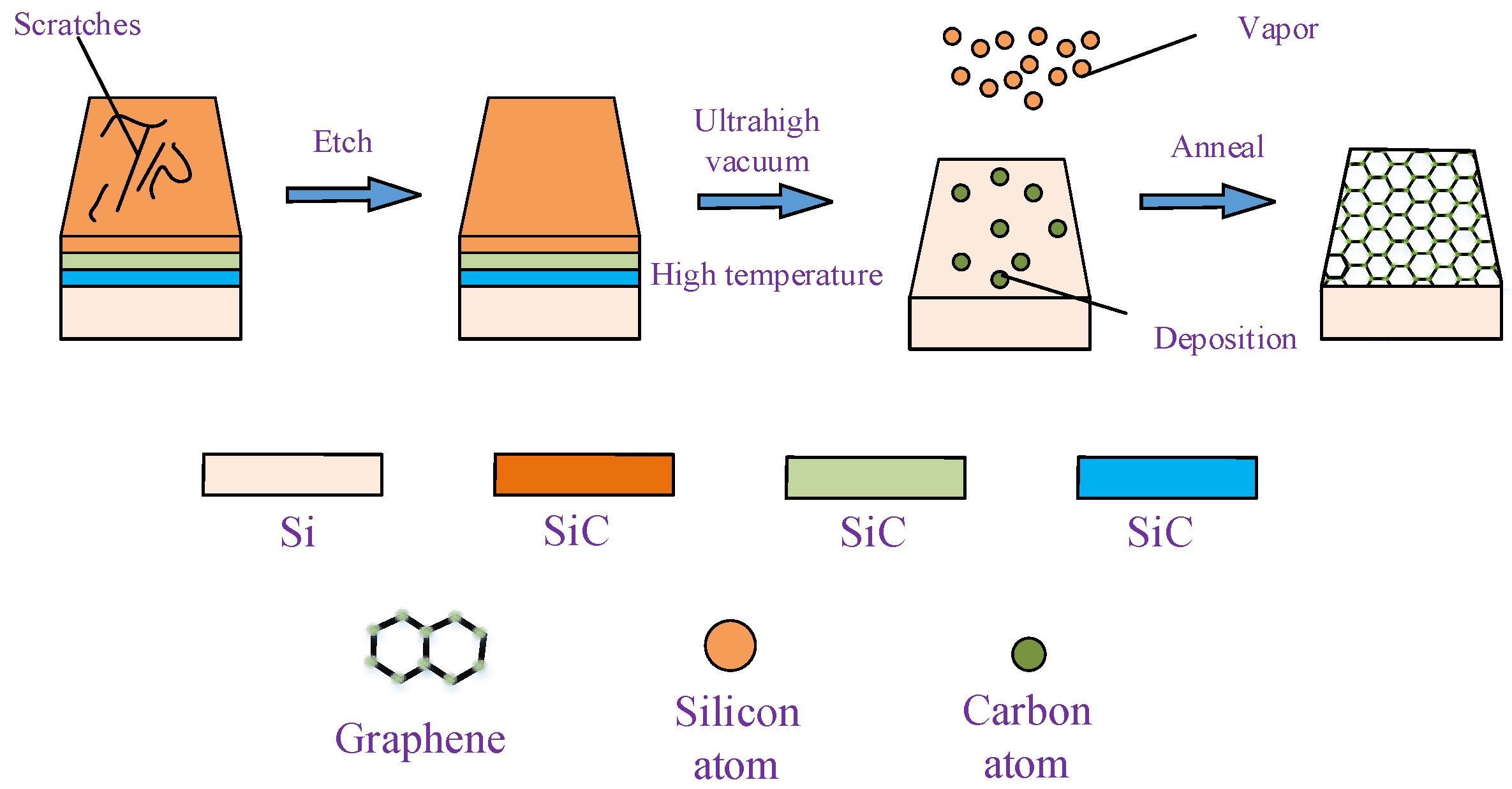
2.1. Epitaxial Growth of Graphene

It was reported in 1962 [18] that when silicon carbide (SiC) is heated to a certain temperature, the silicon carbide shows graphitization and the product always contains amorphous carbon and multilayer graphite. With the development of the epitaxial technique, graphene can be achieved while putting the etching SiC substrate into a high temperature and ultra-high vacuum vessel for a relatively long time. Figure 3 shows the theory of epitaxial growth of graphene. It can be observed that carbide decomposes in the experimental process, and then the carbon atom recombines while non-carbon atoms evaporate. This method is almost based on the SiC substrate, thus the products have a good compatibility with integrated circuits. 6H–SiC and 4H–SiC are often selected to act as the original carbon sources, because both of them have the same Si-C bilayer structure [19,20]. Table 2 is a summary of the epitaxial growth method and the main properties of the synthesized graphene.
Beger and his team [21,26] found that the ultrathin graphene can be synthesized on the surface of 6H–SiC in ultra-high vacuum with about 1 × 10⁻¹⁰ Torr and high temperature that changed from 1250 °C to 1450 °C. The low-energy electron diffraction (LEED) pattern was used to characterize the different growth states of graphene in situ, as shown in Figure 4. It can be seen that with the increase in temperature, the SiC first changes from 1 × 1 pattern to √3 × √3 transition structure, and then a 6√3 × 6√3 unit cell is achieved. Finally, the graphene with charge carrier mobility 1100 cm2·V−1·s−1 at 4 K is achieved.
In order to control the quality of produced graphene, plenty of researchers are dedicated to various kinds of studies on epitaxial growth, such as the investigations of experimental parameters and detection means [23,27,28]. The quality of produced graphene in the ultra-high vacuum is hard to master and has more defects. Meanwhile, excessively high or low temperature also leads to the reduction of graphene quality. When the temperature is excessively high, the number of graphene layers increases. The reflective high energy electron diffraction (RHEED) and the atomic force microscope (AFM) were chosen to study the influence of annealing time, and the results showed that the number of graphene layers is related to the annealing time [24]. The growth pressure was well-controlled by introducing argon (Ar) as a buffer gas into the experimental environment, and the growth mechanism was also discussed by Seyller et al. [25]. They found the charge carrier mobility of the obtained product can reach 2000 cm2·V−1·s−1 at 27 K and explained that the Ar could not only decrease the growth rate and guarantee the growth temperature, but also decrease the vapor rate of silicon atoms.
The graphene could be also synthesized by another carbide, such as titanium carbide (TiC) [29] and tantalum carbide (TaC) [30]. However, these carbides are little studied due to the needs of particular crystal structures and far higher experimental temperature. With the development of other 2D material, hexagonal boron nitride (h-BN) [31] is also regarded as a substrate to epitaxial growth, which is a new idea for further research. The expensive materials and complicated transfer process limit the mass production of graphene. Thus, more attention should be paid to the new carbide than the existing materials, or the manufacturing technique should be changed to maximize profits.

2.2. Chemical Vapor Deposition Mechanism

Chemical vapor deposition (CVD) has the potential to synthesize high-quality graphene that can satisfy the needs of industry. Table 3 shows the typical graphene properties for various kinds of chemical vapor deposition.
Various kinds of materials can be used as substrate to synthesize graphene. Traditional materials, such as copper (Cu) foils and nickel (Ni) are widely employed. Most recently, researchers have paid much attention to other 2D materials, including h-BN [42,43,44] and molybdenum disulfide (MoS2) [45,46]. Cu and Ni can be seen as the representative of low carbon soluble and high carbon soluble materials, respectively. The mechanism to grow graphene on Cu is illustrated in Figure 5. Figure 5a,b show that the surface is etched by hydrogen (H2) at high temperature until there are no obvious scratches. After that, the carbon source and buffer gas are introduced into the reactive system (Figure 5c,d). When the carbon source contacts the Cu at the high temperature, it dissociates into atoms and carbon atoms deposit on the Cu surface. However, because of the low carbon solubility in Cu with 0.008 wt % in 1084 °C [47], the carbon atoms will not further permeate into the Cu. These deposited carbon atoms combine with others to form “graphene islands”; the islands enlarge and further unite to graphene, shown in Figure 5d1,d2.
The high-quality carbon nanotube was grown on the Ni surface using CVD [48]. It was not until 2009 that graphene synthesized on Ni by CVD through improving the experimental parameters and conditions was reported [32,33]. The mechanism is similar to that of growth on Cu, and the difference is shown in Figure 6. Graphene growth on Cu is mainly dependent on self-limiting; however, for Ni it is mainly caused by separating out of the carbon atoms due to the relatively high carbon solubility in Ni with 0.6 wt. % at 1326 °C [47]. It is clear that a carbon source decomposes at high temperature when it contacts the Ni surface. After that, the splitting carbon atoms permeate into Ni to form a solid solution with Ni. Finally, the supersaturated carbon atoms separate out and synthesize graphene on the Ni surface after annealing.

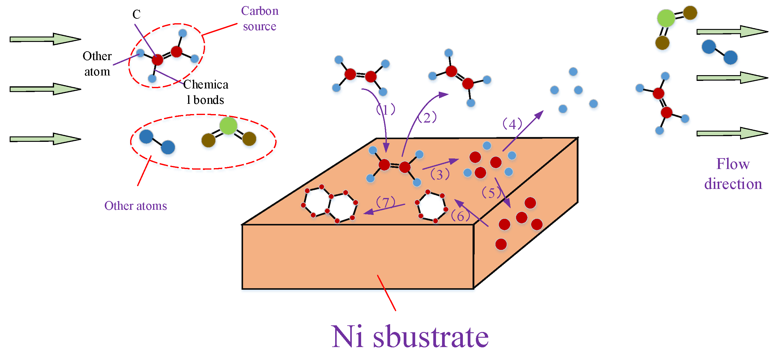
2.2.1. Conventional Chemical Vapor Deposition Growth on Ni

Researchers at the Massachusetts Institute of Technology have systematically studied the growth of graphene on the polycrystalline Ni substrate. Two temperatures, 900 °C and 1000 °C, were studied in different concentrations of methane (CH4) and H2. In addition, the Ni surface was analyzed by transmission electron microscopy (TEM) [32]. As shown in Figure 7, it is clear that the deposited products are graphene and the number of films mainly range from 1 to 8. In subsequent experiments, the coverage of about 87% of monolayer and bilayer graphene were achieved in the ambient pressure by controlling the CH4 concentration and cooling speed of polycrystalline Ni substrate [49]. Ar was also introduced into the CVD method as a buffer gas and a cooling gas [33]. The 300 nm thick nickel layer on the Si wafer was put in the atmosphere of mixed gases (Ar, H2 and CH4) and high temperature of 1000 °C, then the substrate was quickly cooled down to about 25 °C. The number of obtained graphene layers was less than 10. They found that the quality of produced graphene is positively related to the cooling rate. Optical image and Raman spectrum were used to identify the film after being transferred to SiC, as shown in Figure 8. The typical feature for graphene in Raman spectrum is characterized with a G peak (~1580 cm−1), D peak (~1345 cm−1) and 2D peak (~2700 cm−1). In addition, the number of graphene films can be deduced by the ratio of the intensities of 2D peak and G peak [32].
Other parameters have also been discussed in recent years. The difference of grain of Ni was reported by Zhou et al. [50]. They found that because of the atomically smooth surface of single crystalline Ni, the area of monolayer or bilayer graphene deposited on single crystalline Ni (91.4%) is much bigger than that for polycrystalline Ni (72.8%) [50]. Choi et al. [51] systematically studied the mechanism of wrinkle formation and provided optimized parameters to synthesize graphene on single-crystalline Ni through changing the proportion of precursor gases, experimental temperature and deposited time. In order to decrease the cost, various kinds of carbon sources, such as soya-bean oil [34], have been presented.

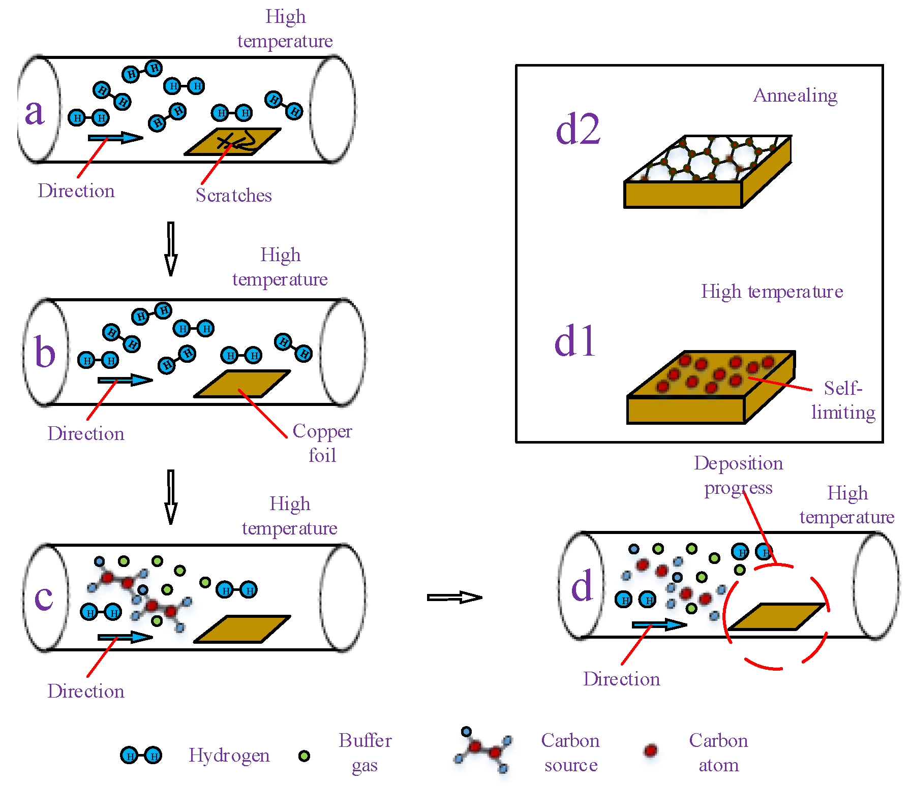
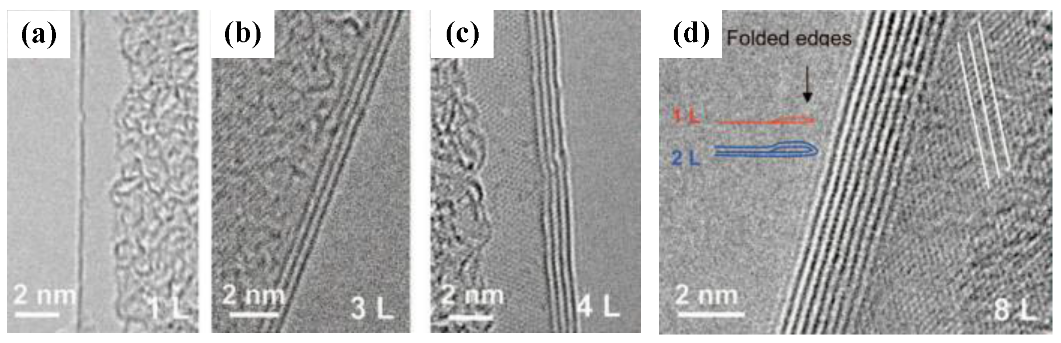
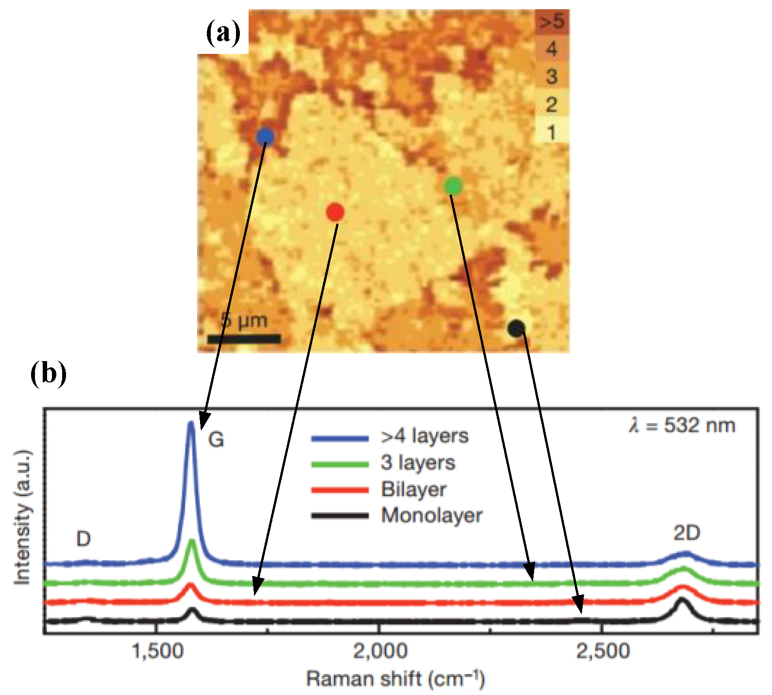
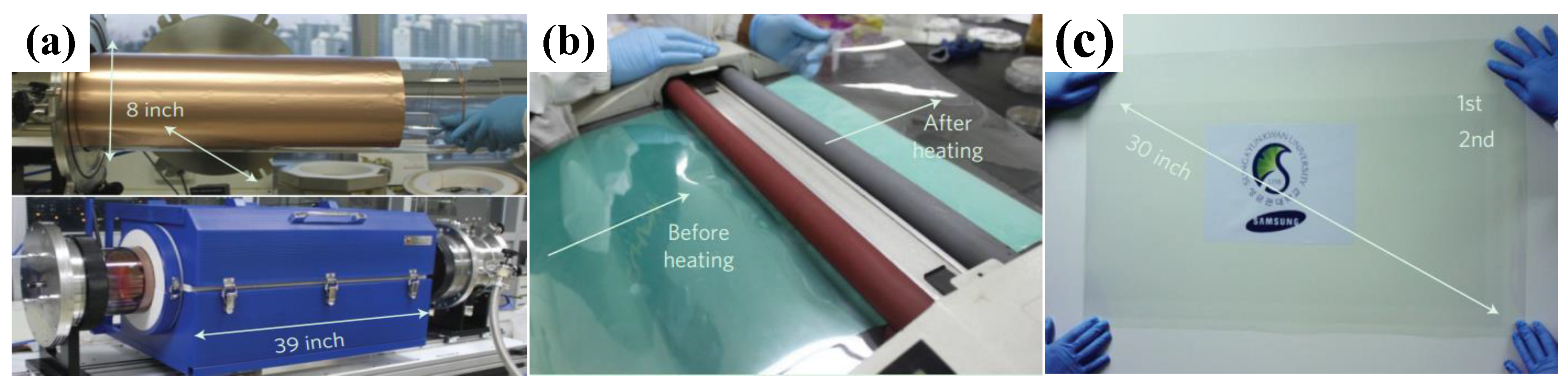
2.2.2. Conventional Chemical Vapor Deposition Growth on Cu

It is possible to produce high-quality graphene with fewer layers using Cu foil as substrate. Ruoff et al. [35] have synthesized monolayer graphene on the 25 μm thick Cu foil in high temperature conditions (1000 °C) and mixture gases (CH4 and H2). The number of graphene layers is lower than 3, and the area of monolayer graphene is more than 95%.
Since then, various research has discussed the effect of experimental parameters to deposit uniform graphene films on the Cu foils, including experimental pressure, time and carbon sources. At a pressure of 340 Pa, graphene is grown on the surface of Cu foil in different times, i.e., 20 min, 80 min, 120 min and 180 min [52]. The optical images in Figure 9 show that with the increase in experimental time, the substrate surface becomes much smoother, thus the growth of bilayer graphene is suppressed and large-scale monolayer graphene is achieved. [46]. Vlassiouk and Smirnov [53] paid much attention on growth temperature and pointed out that the experimental temperature, which is similar to the melting point of Cu foil, contributes to the synthesis of high-quality graphene in the atmospheric pressure. They [53] explained that the sublimation of Cu atoms are restrained and more energy is used for desorption of carbon clusters in that temperature. The influences of growth temperature, CH4 flow rate and annealing temperature were intensively studied to synthesize high-quality graphene at ambient pressure. The results showed that higher annealing temperature and lower growth temperature contribute to the synthesis of monolayer graphene [54]. In order to obtain graphene at a large scale, roll-to-roll production technology was introduced into the CVD system. In addition, graphene in one 30-inch layer was produced on the ultra-large copper substrate, which can be seen in Figure 10 [36]. Polystyrene was chosen to produce carbon atoms, and monolayer graphene with a coverage of 97.5% on the substrate was achieved in a short time (about 3 min) [37].
Meanwhile, researchers focused on the measurement means for exploring the growth progress to produce high-quality graphene [55,56,57,58]. For example, the isotope-labelling method and nano angle resolved photoelectron spectroscope (Nano-ARPES) were employed by Ruoff et al. [55] and Asensio et al. [57], respectively. Different substrates, including platinum (Pt) [59], iridium (Ir) [60] and germanium (Ge) [61,62] have also been mentioned. It was first reported that the graphene deposited on the Co/MgO substrate has better application prospects for molecular electronics and polymer composites [63]. To reduce energy consumption and deposit graphene directly on the electronic device, using low temperature to synthesize graphene has become a research hot spot. Various kinds of CVD methods, including hydrogen-free chemical vapor deposition (HFCVD) [64], carbon-enclosed chemical vapor deposition (CECVD) [65], plasma enhanced chemical vapor deposition (PECVD) [66], ultra-high vacuum chemical vapor deposition (UHVCVD) [67] and oxygen-free chemical vapor deposition (OFCVD) [68] method, are presented. Cho and Hong et al. [64] tried to decrease the experimental temperature, however the temperature only reduced from 1000 °C to 970 °C. Jang et al. [68] developed an oxygen-free chemical method which removed the oxygen and successfully used low activation energy benzene as carbon source to synthesize graphene on Cu foils at atmospheric pressure at 300 °C.

2.2.3. Plasma-Enhanced Chemical Vapor Deposition

Graphene can be achieved by conventional chemical vapor deposition, and different CVD methods are explored that have been previously mentioned. Based on the development of plasma technology and requirements of low energy [69], the plasma-enhanced chemical vapor deposition method has been studied [70,71].
In the microwave-assisted deposition progress, high-energy electrons can provide enough activation energy. Once the plasma gases collide with carbon sources, bands of reactive gas are broken and the chemical activity of precursor gases increases. Thus, the experimental temperature decreases. Following this, some atoms recombine with other atoms before coming into contact with the substrate, and some carbon atoms may deposit on the surface of the substrate or permeate into the substrate. After annealing, graphene is synthesized on the substrate surface.
Graphene has been successfully synthesized by microwave-assisted deposition technology at low experimental temperature. For example, a few layers of graphene can be synthesized in the phenomenon of CH4 and H2 when the temperature is 700 °C [38]. The synthesized graphene is vertically grown on the substrates, and the number of obtained graphene layers are mainly within the range of 4 to 6 [38]. Moreover, Boyd et al. [39] used Cu foil as a substrate to grow graphene in a relative low temperature (below 420 °C) and the deposition time was just a few minutes. Just as with conventional chemical vapor deposition, different materials that are used as carbon sources are discussed in the studies. Tatarova et al. [72] chose ethyl alcohol as a carbon source to deposit graphene on the surface of a cavity wall and found that the contents of monolayer graphene decrease when the wall’s temperature increases from 60 to 100 °C. In addition, when the temperature is 60 °C, the ordered crystal edges are observed. However, with the temperature increasing to 80 °C, the contents of monolayer graphene are clearly reducing. Furthermore, researchers have also paid much attention to various kinds of growth substrates. For example, Song et al. [73] attempted to grow a few graphene layers on metal and nonmetal substrates at low temperature.
The size of graphene limits its further application, and large-scale graphene is desperately needed in many industries. Yamada et al. [74] combined roll-to-roll technology and microwave-assisted chemical vapor deposition technology to build a new graphene preparation system. The mixed gases (CH4, H2 and Ar) flowed into this system, and graphene film with dimensions 294 mm × 480 mm was achieved at 400 °C. Dato at the University of California, Berkeley proved [40,75,76] that graphene can be synthesized without substrate through presenting a novel microwave-assisted equipment, as shown in Figure 11. Ethanol droplets flowed through the Ar plasma and graphene was collected in the upper nylon filter. The deposition velocity reached about 2 mg/min. They also found that this method is not fit for CH4 and isopropanol, and lower velocity contributes to the synthesis graphite instead of graphene.
The arc discharge method is another plasma technology that attracts researchers’ attentions. Two graphite electrodes are regarded as the carbon source and arc plasma is generated between the two graphite electrodes in the presence of Ar, helium (He) or H2. Finally, graphene is deposited on the cathodic electrode, reactor wall or special substrates. Nowadays, graphene is successfully synthesized by arc plasma technology, but the control progress should be improved. Rao et al. [41] used direct current arc to vapor anode graphite rod in the phenomenon of H2, and the number of produced graphene layers was less than 4. They also found that the present of H2 suppresses the product, changing from graphene to carbon nanotubes. In order to conveniently distinguish the carbon nanotubes from graphene, magnetic fields were introduced by Ostrikov et al. [77,78]. Figure 12 shows the schematic diagram of the arc plasma method in the magnetic field. It can be observed that the carbon nanotubes and graphene are deposited on different area of a magnet. The effects of the experimental parameters are also discussed. The effect of pressure changing from 400 Torr to 1000 Torr was reported in 2010 and the results showed that with the increase of experimental pressure, graphene with higher quality would be achieved [79]. In addition, the effect of buffer gas, which acts as coolant, has already been studied [80]. As mentioned before, the control mechanism should be further investigated to meet the needs of industrialization.

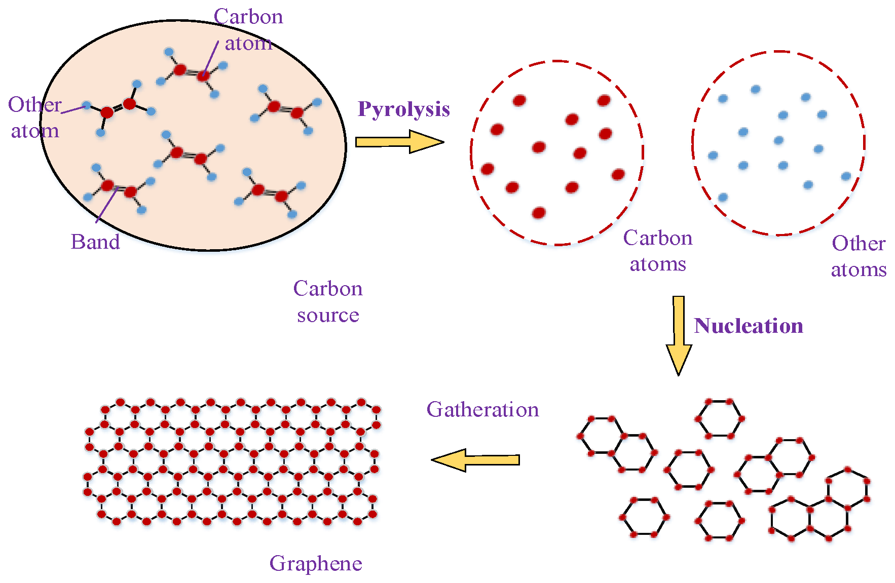
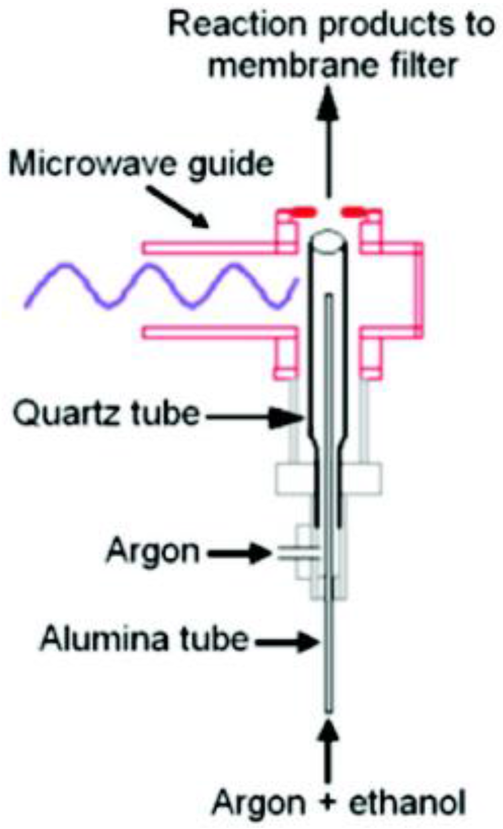
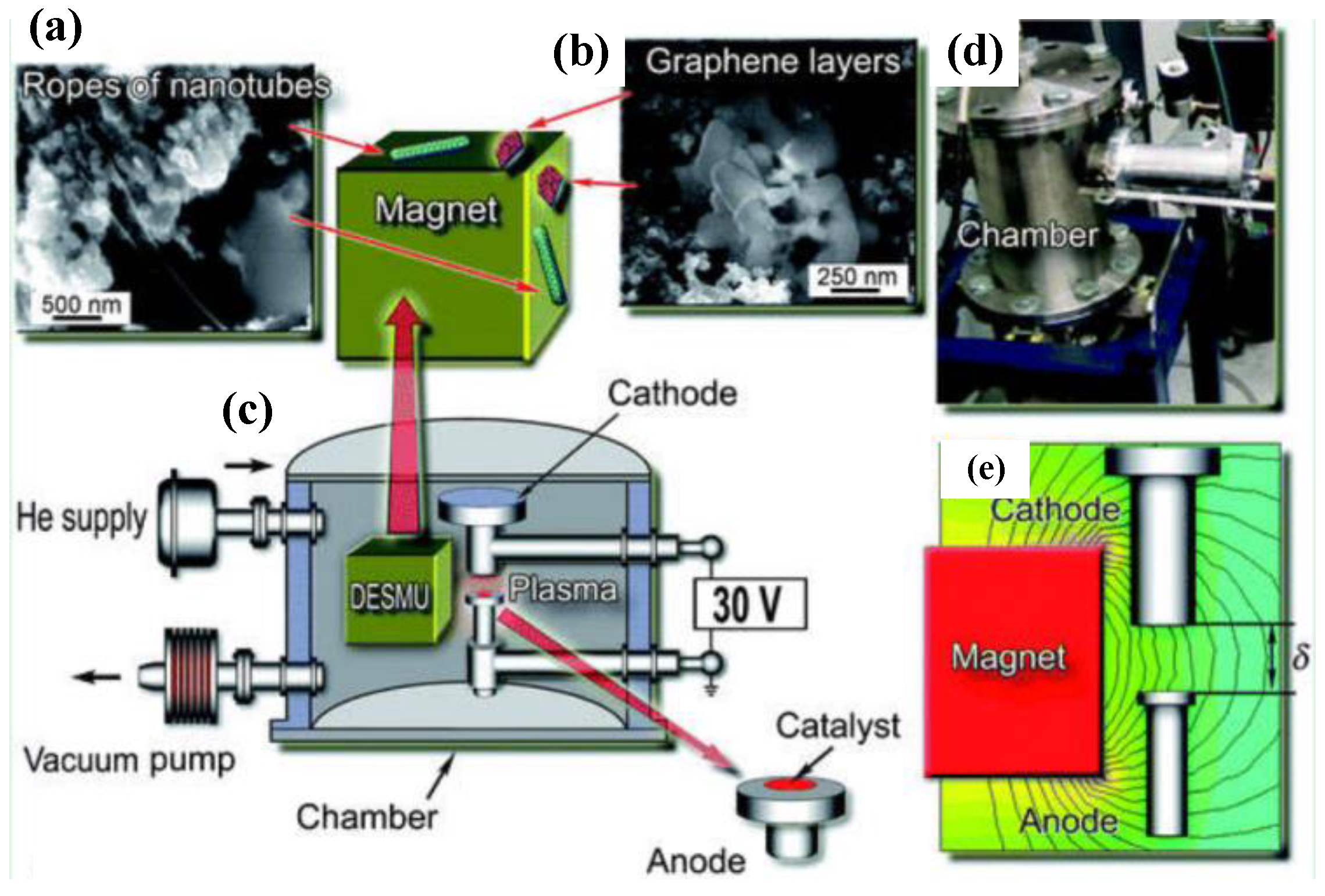
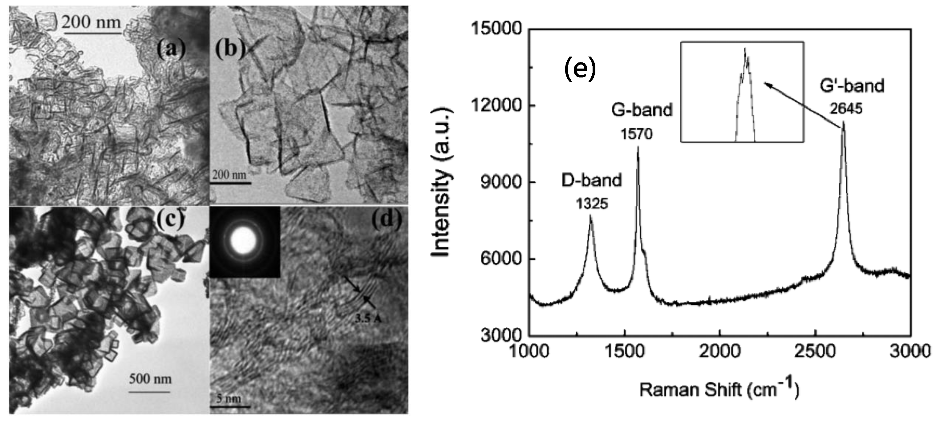
2.3. Combustion Method

The combustion method is regarded as one of the greatest potential technologies for producing carbon materials at a large scale. A homemade set-up was built to synthesize graphene, the mixture gases of oxygen and ethylene were injected into a hydrostatic column with a press-seal of a maximum capacity 16.6 L, and then the spark plug was ignited for combustion. After that, graphene was achieved. Moreover, the different mixture ratios of oxygen and ethylene were investigated, and the ideal ratio was 0.6. When the combustion temperature is below 4000 K, the synthesized product is charcoal instead of graphene [81,82]. A much simpler experimental facility was invented in Tsinghua University, and this set-up consisted of alcohol burner and butane lamp. The alcohol burner was used to provide a protective flame atmosphere, meanwhile the carbon atoms and the needed temperature were produced by butane lamp. The graphene finally deposited on the surface of Ni substrate in a short time [83]. The experimental facility was improved by Tse et al., and the much lower oxygen content graphene was synthesized [84].
Another combustion method has been studied by Xiao et al. [85], who put magnesium (Mg) into a carbon dioxide (CO2) atmosphere. After combusting, the black product was analyzed by TEM and Raman spectrum and the material was proved to be graphene with fewer than 10 layers, as shown in Figure 13. The mechanism is discussed and the reactive progress is shown as Equation (1). Graphene can also be achieved by combustion of calcium (Ca) in the presence of CO2 and the mechanism is shown in Equation (2) [86].
2Mg + CO2 = 2MgO + C
2Ca + CO2 = 2CaO + C
How to choose these three methods is also a question, thus a comparison of experimental temperature, energy cost, throughput and electrical properties of different synthesis methods is given in Table 4. This table is beneficial for further consideration of the cost and the return on investment in different methods.

3. Conclusions

The progress in synthesis of high-quality and large-scale graphene is worthy of praise, especially in the field of fundamental research. However, the challenge still exists in the real world. The structural controllability and membrane homogeneity are big puzzles that researchers are faced with. In this paper, the mechanism of the thermal growth method has been discussed in detail and three different thermal growth methods have been presented. These methods are all based on splitting decomposition of molecules and recrystallization of atoms. Epitaxial growth of graphene, which synthesize graphene in relative high quality, is widely used in electronic products due to the possibility of graphene being directly grown on SiC. Chemical vapor deposition possesses the unique advantage of producing large-scale graphene, and becomes a research priority. The combustion method has the lowest requirement for experimental facility and an open experimental environment, which catches investigators’ attentions. However, the quality of graphene made by this method is very poor.
Nowadays, new 2D materials, such as h-BN and MoS2, have been used to act as a substrate to synthesize graphene, and these products have much better performance. That is to say, proper optimizing experimental parameters, such as deposition time and temperature, can improve the quality of graphene. The introduction of plasma and roll-to-roll technology has proved that new technology may promote the development of graphene synthesis. Researchers should pay attention not only to the existing methods, but also to the latest technologies. Novel combinations of existing technologies are needed. In order to reduce cost and improve the quality of transferred graphene, it is better to synthesize graphene on target substrates, or a new and undamaged transfer technology should be presented. More efforts should also be made on the reduction of energy consumption and the simplification of equipment.

Acknowledgments

This research is supported by the Beijing Natural Science Foundation (No. 3162024), Tribology Science Foundation of State Key laboratory of Tribology (No. SKLTKF14A08), and Science Foundation of China University of Petroleum, Beijing (No. 2462017BJB06, C201602).

Conflicts of Interest

The authors declare no conflict of interest.

References

  1. Peierls, R.E. Bemerkungen über umwandlungstemperaturen. Helv. Phys. Acta 1934, 7, 81–83. (In German) [Google Scholar]
  2. Peierls, R.E. Quelques proprietes typiques des corpses solides. Ann. I. H. Poincare 1935, 5, 177–222. (In German) [Google Scholar]
  3. Landau, L.D. Zur Theorie der phasenumwandlungen II. Phys. Z. Sowjetunion 1937, 11, 26–35. (In German) [Google Scholar]
  4. Novoselov, K.S.; Geim, A.K.; Morozov, S.V.; Jiang, D.; Zhang, Y.; Dubonos, S.V.; Grigorieva, I.V.; Firsov, A.A. Electric field effect in atomically thin carbon films. Science 2004, 306, 666–669. [Google Scholar] [CrossRef] [PubMed]
  5. Kroto, H.W.; Heath, J.R.; O’Brien, S.C.; Curl, R.F.; Smalley, R.E. C60: Buckminsterfullerene. Nature 1985, 318, 162–163. [Google Scholar] [CrossRef]
  6. Iijima, S. Helical microtubules of graphitic carbon. Nature 1991, 354, 56–58. [Google Scholar] [CrossRef]
  7. Zhang, Y.; Tan, Y.W.; Stormer, H.L.; Kim, P. Experimental observation of the quantum hall effect and berry’s phase in graphene. Nature 2005, 438, 201–204. [Google Scholar] [CrossRef] [PubMed]
  8. Sweetman, M.J.; May, S.; Mebberson, N.; Pendleton, P.; Vasilev, K.; Plush, S.E.; Hayball, J.D. Activated carbon, carbon nanotubes and graphene: Materials and composites for advanced water purification. C 2017, 3, 18. [Google Scholar] [CrossRef]
  9. Liu, B.; Xie, J.; Ma, H.; Zhang, X.; Pan, Y.; Lv, J.; Ge, H.; Ren, N.; Su, H.; Xie, X.; et al. From graphite to graphene oxide and graphene oxide quantum dots. Small 2017, 13. [Google Scholar] [CrossRef] [PubMed]
  10. Buzaglo, M.; Bar, I.P.; Varenik, M.; Shunak, L.; Pevzner, S.; Regev, O. Graphite-to-Graphene: Total conversion. Adv. Mater. 2017, 29. [Google Scholar] [CrossRef] [PubMed]
  11. Mayorov, A.S.; Gorbachev, R.V.; Morozov, S.V.; Britnell, L.; Jalil, R.; Ponomarenko, L.A.; Blake, P.; Novoselov, K.S.; Watanabe, K.; Taniguchi, T.; et al. Micrometer-scale ballistic transport in encapsulated graphene at room temperature. Nano Lett. 2011, 11, 2396–2399. [Google Scholar] [CrossRef] [PubMed]
  12. Lee, C.; Wei, X.; Kysar, J.W.; Hone, J. Measurement of the elastic properties and intrinsic strength of monolayer graphene. Science 2008, 321, 385–388. [Google Scholar] [CrossRef] [PubMed]
  13. Balandin, A.A.; Ghosh, S.; Bao, W.; Calizo, I.; Teweldebrhan, D.; Miao, F.; Lau, C.N. Superior thermal conductivity of single-layer graphene. Nano Lett. 2008, 8, 902–907. [Google Scholar] [CrossRef] [PubMed]
  14. Nair, R.R.; Blake, P.; Grigorenko, A.N.; Novoselov, K.S.; Booth, T.J.; Stauber, T.; Peres, N.M.R.; Geim, A.K. Fine structure constant defines visual tranparency of graphene. Science 2008, 320, 1308. [Google Scholar] [CrossRef] [PubMed]
  15. Yi, M.; Shen, Z. A review on mechanical exfoliation for the scalable production of graphene. J. Mater. Chem. A 2015, 3, 11700–11715. [Google Scholar] [CrossRef]
  16. Ponomarenko, L.A.; Schedin, F.; Katsnelson, M.I.; Yang, R.; Hill, E.W.; Novoselov, K.S.; Geim, A.K. Chaotic Dirac billiard in graphene quantum dots. Science 2008, 320, 356–358. [Google Scholar] [CrossRef] [PubMed]
  17. Lin, Y.M.; Dimitrakopoulos, C.; Jenkins, K.A.; Farmer, D.B.; Chiu, H.Y.; Grill, A.; Avouris, P. 100-GHz transistors from wafer-scale epitaxial graphene. Science 2010, 327, 662. [Google Scholar] [CrossRef] [PubMed]
  18. Badami, D.V. Graphitization of α-silicon carbide. Nature 1962, 193, 569–570. [Google Scholar] [CrossRef]
  19. Hass, J.; Millán-Otoya, J.E.; First, P.N.; Conrad, E.H. Interface structure of epitaxial graphene grown on 4H-SiC (0001). Phys. Rev. B 2008, 78, 205424. [Google Scholar] [CrossRef]
  20. Jernigan, G.G.; VanMil, B.L.; Tedesco, J.L.; Tischler, J.G.; Glaser, E.R.; Davidson, A., III; Campbell, P.M.; Gaskill, D.K. Comparison of epitaxial graphene on Si-face and C-face 4H SiC formed by ultrahigh vacuum and RF furnace production. Nano Lett. 2009, 9, 2605–2609. [Google Scholar] [CrossRef] [PubMed]
  21. Berger, C.; Song, Z.; Li, T.; Li, X.; Ogbazghi, A.Y.; Feng, R.; Dai, Z.; Marchenkov, A.N.; Conrad, E.H.; First, P.N.; et al. Ultrathin epitaxial graphite: 2D electron gas properties and a route toward graphene-based nanoelectronics. J. Phys. Chem. B 2004, 108, 19912–19916. [Google Scholar] [CrossRef]
  22. Berger, C.; Song, Z.; Li, X.; Wu, X.; Brown, N.; Naud, C.; Mayou, D.; Li, T.; Hass, J.; Marchenkov, A.N.; et al. Electronic confinement and coherence in patterned epitaxial graphene. Science 2006, 312, 1191–1196. [Google Scholar] [CrossRef] [PubMed]
  23. Kang, C.Y.; Fan, L.L.; Chen, S.; Liu, Z.L.; Xu, P.S.; Zou, C.W. Few-layer graphene growth on 6H-SiC (0001) surface at low temperature via Ni-silicidation reactions. Appl. Phys. Lett. 2012, 100, 251604. [Google Scholar] [CrossRef]
  24. Tang, J.; Liu, Z.L.; Kang, C.Y.; Yan, W.S.; Xu, P.S.; Pan, H.B.; Wei, S.Q.; Gao, Y.Q.; Xu, X.G. Annealing time dependence of morphology and structure of epitaxial graphene on 6H-SiC(0001) surface. Acta Phys-Chim. Sin. 2010, 26, 253–258. (In Chinese) [Google Scholar]
  25. Emtsev, K.V.; Bostwick, A.; Horn, K.; Jobst, J.; Kellogg, G.L.; Ley, L.; McChesney, J.L.; Ohta, T.; Reshanov, S.A.; Röhrl, J.; et al. Towards wafer-size graphene layers by atmospheric pressure graphitization of silicon carbide. Nat. Mater. 2009, 8, 203–207. [Google Scholar] [CrossRef] [PubMed]
  26. Heer, W.A.D.; Berger, C.; Wu, X.; First, P.N.; Conrad, E.H.; Li, X.; Li, T.; Sprinkle, M.; Hass, J.; Sadowski, M.L.; et al. Epitaxial graphene. Solid State Commun. 2007, 143, 92–100. [Google Scholar] [CrossRef]
  27. Hass, J.; De Heer, W.A.; Conrad, E.H. The growth and morphology of epitaxial multilayer graphene. J. Phys. Condens. Matter 2008, 20, 323202. [Google Scholar] [CrossRef]
  28. Hicks, J.; Shepperd, K.; Wang, F.; Conrad, E.H. The structure of graphene grown on the SiC surface. J. Phys. D Appl. Phys. 2012, 45, 154002. [Google Scholar] [CrossRef]
  29. Terai, M.; Hasegawa, N.; Okusawa, M.; Otani, S.; Oshima, C. Electronic states of monolayer micrographite on TiC (111)-faceted and TiC (410) surfaces. Appl. Surf. Sci. 1998, 130, 876–882. [Google Scholar] [CrossRef]
  30. Itchkawitz, B.S.; Lyman, P.F.; Ownby, G.W.; Zehner, D.M. Monolayer graphite on TaC (111): Electronic band structure. Surf. Sci. 1994, 318, 395–402. [Google Scholar] [CrossRef]
  31. Yang, W.; Chen, G.; Shi, Z.; Liu, C.C.; Zhang, L.; Xie, G.; Cheng, M.; Wang, D.; Yang, R.; Shi, D.; et al. Epitaxial growth of single-domain graphene on hexagonal boron nitride. Nat. Mater. 2013, 12, 792–797. [Google Scholar] [CrossRef] [PubMed]
  32. Reina, A.; Jia, X.; Ho, J.; Nezich, D.; Son, H.; Bulovic, V.; Dresselhaus, M.S.; Kong, J. Large area, few-layer graphene films on arbitrary substrates by chemical vapor deposition. Nano Lett. 2009, 9, 30–35. [Google Scholar] [CrossRef] [PubMed]
  33. Kim, K.S.; Zhao, Y.; Jang, H.; Lee, S.Y.; Kim, J.M.; Kim, K.S.; Ahn, J.H.; Kim, P.; Choi, J.Y.; Hong, B.H. Large-scale pattern growth of graphene films for stretchable transparent electrodes. Nature 2009, 457, 706–710. [Google Scholar] [CrossRef] [PubMed]
  34. Seo, D.H.; Pineda, S.; Fang, J.; Gozukara, Y.; Yick, S.; Bendavid, A.; Lam, S.K.H.; Murdock, A.T.; Murphy, A.B.; Han, Z.J.; et al. Single-step ambient-air synthesis of graphene from renewable precursors as electrochemical genosensor. Nat. Commun. 2017, 8, 14217. [Google Scholar] [CrossRef] [PubMed]
  35. Li, X.; Cai, W.; An, J.; Kim, S.; Nah, J.; Yang, D.; Piner, R.; Velamakanni, A.; Jung, I.; Tutuc, E.; et al. Large-area synthesis of high-quality and uniform graphene films on copper foils. Science 2009, 324, 1312–1314. [Google Scholar] [CrossRef] [PubMed]
  36. Bae, S.; Kim, H.; Lee, Y.; Xu, X.; Park, J.S.; Zheng, Y.; Balakrishnan, J.; Lei, T.; Kim, H.R.; Song, Y., II; et al. Roll-to-roll production of 30-inch graphene films for transparent electrodes. Nat. Nanotechnol. 2010, 5, 574–578. [Google Scholar] [CrossRef] [PubMed]
  37. Xu, J.; Fu, C.; Sun, H.; Meng, L.; Xia, Y.; Zhang, C.; Yi, X.; Yang, W.; Guo, P.; Wang, C.; et al. Large-area, high-quality monolayer graphene from polystyrene at atmospheric pressure. Nanotechnology 2017, 28, 155605. [Google Scholar] [CrossRef] [PubMed]
  38. Malesevic, A.; Vitchev, R.; Schouteden, K.; Volodin, A.; Zhang, L.; Van Tendeloo, G.; Vanhulsel, A.; Van Haesendonck, C. Synthesis of few-layer graphene via microwave plasma-enhanced chemical vapor deposition. Nanotechnology 2008, 19, 305604. [Google Scholar] [CrossRef] [PubMed]
  39. Boyd, D.A.; Lin, W.H.; Hsu, C.C.; Teague, M.L.; Chen, C.C.; Lo, Y.Y.; Chan, W.Y.; Su, W.B.; Cheng, T.C.; Chang, C.S.; et al. Single-step deposition of high-mobility graphene at reduced temperatures. Nat. Commun. 2015, 6, 6620. [Google Scholar] [CrossRef] [PubMed]
  40. Dato, A.; Radmilovic, V.; Lee, Z.; Phillips, J.; Frenklach, M. Substrate-free gas-phase synthesis of graphene sheets. Nano Lett. 2008, 8, 2012–2016. [Google Scholar] [CrossRef] [PubMed]
  41. Subrahmanyam, K.S.; Panchakarla, L.S.; Govindaraj, A.; Rao, C.N.R. Simple method of preparing graphene flakes by an arc-discharge method. J. Phys. Chem. C 2009, 113, 4257–4259. [Google Scholar] [CrossRef]
  42. Son, M.; Lim, H.; Hong, M.; Choi, H.C. Direct growth of graphene pad on exfoliated hexagonal boron nitride surface. Nanoscale 2011, 3, 3089–3093. [Google Scholar] [CrossRef] [PubMed]
  43. Tang, S.; Ding, G.; Xie, X.; Chen, J.; Wang, C.; Ding, X.; Huang, F.; Lu, W.; Jiang, M. Nucleation and growth of single crystal graphene on hexagonal boron nitride. Carbon 2012, 50, 329–331. [Google Scholar] [CrossRef]
  44. Liu, Z.; Song, L.; Zhao, S.; Huang, J.; Ma, L.; Zhang, J.; Lou, J.; Ajayan, P.M. Direct growth of graphene/hexagonal boron nitride stacked layers. Nano Lett. 2011, 11, 2032–2037. [Google Scholar] [CrossRef] [PubMed]
  45. Kwieciñski, W.; Sotthewes, K.; Poelsema, B.; Zandvliet, H.J.; Bampoulis, P. Chemical vapor deposition growth of bilayer graphene in between molybdenum disulfide sheets. J. Colloid Interface Sci. 2017, 505, 776–782. [Google Scholar] [CrossRef] [PubMed]
  46. Fu, W.; Du, F.H.; Su, J.; Li, X.H.; Wei, X.; Ye, T.N.; Wang, K.X.; Chen, J.S. In situ catalytic growth of large-area multilayered graphene/MoS2 heterostructures. Sci. Rep. 2014, 4, 4673. [Google Scholar] [CrossRef] [PubMed]
  47. Oshima, C.; Nagashima, A. Ultra-thin epitaxial films of graphite and hexagonal boron nitride on solid surfaces. J. Phys. Condens. Matter 1997, 9, 1. [Google Scholar] [CrossRef]
  48. Kong, J.; Cassell, A.M.; Dai, H. Chemical vapor deposition of methane for single-walled carbon nanotubes. Chem. Phys. Lett. 1998, 292, 567–574. [Google Scholar] [CrossRef]
  49. Reina, A.; Thiele, S.; Jia, X.; Bhaviripudi, S.; Dresselhaus, M.S.; Schaefer, J.A.; Kong, J. Growth of large-area single-and bi-layer graphene by controlled carbon precipitation on polycrystalline Ni surfaces. Nano Res. 2009, 2, 509–516. [Google Scholar] [CrossRef] [Green Version]
  50. Zhang, Y.; Gomez, L.; Ishikawa, F.N.; Madaria, A.; Ryu, K.; Wang, C.; Badmaev, A.; Zhou, C. Comparison of graphene growth on single-crystalline and polycrystalline Ni by chemical vapor deposition. J. Phys. Chem. Lett. 2010, 1, 3101–3107. [Google Scholar] [CrossRef]
  51. Chae, S.J.; Güneş, F.; Kim, K.K.; Kim, E.S.; Han, G.H.; Kim, S.M.; Shin, H.J.; Yoon, S.M.; Choi, J.Y.; Park, M.H.; et al. Synthesis of large-area graphene layers on poly-nickel substrate by chemical vapor deposition: Wrinkle formation. Adv. Mater. 2009, 21, 2328–2333. [Google Scholar] [CrossRef]
  52. Liu, J.; Li, P.; Chen, Y.; Wang, Z.; He, J.; Tian, H.; Qi, F.; Zheng, B.; Zhou, J.; Lin, W.; et al. Large-area synthesis of high-quality and uniform monolayer graphene without unexpected bilayer regions. J. Alloys Compd. 2014, 615, 415–418. [Google Scholar] [CrossRef]
  53. Vlassiouk, I.; Smirnov, S.; Regmi, M.; Surwade, S.P.; Srivastava, N.; Feenstra, R.; Eres, G.; Parish, C.; Lavrik, N.; Datskos, P.; et al. Graphene nucleation density on copper: Fundamental role of background pressure. J. Phys. Chem. C 2013, 117, 18919–18926. [Google Scholar] [CrossRef]
  54. Liu, L.; Zhou, H.; Cheng, R.; Chen, Y.; Lin, Y.C.; Qu, Y.; Bai, J.; Ivanov, I.A.; Liu, G.; Huang, Y.; et al. A systematic study of atmospheric pressure chemical vapor deposition growth of large-area monolayer graphene. J. Mater. Chem. 2012, 22, 1498–1503. [Google Scholar] [CrossRef] [PubMed]
  55. Li, X.; Cai, W.; Colombo, L.; Ruoff, R.S. Evolution of graphene growth on Ni and Cu by carbon isotope labeling. Nano Lett. 2009, 9, 4268–4272. [Google Scholar] [CrossRef] [PubMed]
  56. Whiteway, E.; Yang, W.; Yu, V.; Hilke, M. Time evolution of the growth of single graphene crystals and high resolution isotope labeling. Carbon 2017, 111, 173–181. [Google Scholar] [CrossRef]
  57. Chen, C.; Avila, J.; Asensio, M.C. Chemical and electronic structure imaging of graphene on Cu: A NanoARPES study. J. Phys. Condens. Matter 2017, 29, 183001. [Google Scholar] [CrossRef] [PubMed]
  58. Yang, F.; Liu, Y.; Wu, W.; Chen, W.; Gao, L.; Sun, J. A facile method to observe graphene growth on copper foil. Nanotechnology 2012, 23, 475705. [Google Scholar] [CrossRef] [PubMed]
  59. Vinogradov, N.A.; Schulte, K.; Ng, M.L.; Mikkelsen, A.; Lundgren, E.; Martensson, N.; Preobrajenski, A.B. Impact of atomic oxygen on the structure of graphene formed on Ir (111) and Pt (111). J. Phys. Chem. C 2011, 115, 9568–9577. [Google Scholar] [CrossRef]
  60. Coraux, J.; Engler, M.; Busse, C.; Wall, D.; Buckanie, N.; Zu Heringdorf, F.J.M.; Van Gastel, R.; Poelsema, B.; Michely, T. Growth of graphene on Ir (111). New J. Phys. 2009, 11, 023006. [Google Scholar] [CrossRef]
  61. Lukosius, M.; Dabrowski, J.; Kitzmann, J.; Fursenko, O.; Akhtar, F.; Lisker, M.; Lippert, G.; Schulze, S.; Yamamoto, Y.; Schubert, M.A.; et al. Metal-free CVD graphene synthesis on 200 mm Ge/Si (001) substrates. ACS Appl. Mater. Interfaces 2016, 8, 33786–33793. [Google Scholar] [CrossRef] [PubMed]
  62. Scaparro, A.M.; Miseikis, V.; Coletti, C.; Notargiacomo, A.; Pea, M.; De Seta, M.; Di Gaspare, L. Investigating the CVD Synthesis of Graphene on Ge (100): Toward layer-by-layer growth. ACS Appl. Mater. Interfaces 2016, 8, 33083–33090. [Google Scholar] [CrossRef] [PubMed]
  63. Wang, X.; You, H.; Liu, F.; Li, M.; Wan, L.; Li, S.; Li, Q.; Xu, Y.; Tian, R.; Yu, Z.; et al. Large-scale synthesis of few-layered graphene using CVD. Chem. Vapor Depos. 2009, 15, 53–56. [Google Scholar] [CrossRef]
  64. Ryu, J.; Kim, Y.; Won, D.; Kim, N.; Park, J.S.; Lee, E.K.; Cho, D.; Cho, S.P.; Kim, S.J.; Ryu, G.H.; et al. Fast synthesis of high-performance graphene films by hydrogen-free rapid thermal chemical vapor deposition. ACS Nano 2014, 8, 950–956. [Google Scholar] [CrossRef] [PubMed]
  65. Chen, Y.Z.; Medina, H.; Tsai, H.W.; Wang, Y.C.; Yen, Y.T.; Manikandan, A.; Chueh, Y.L. Low temperature growth of graphene on glass by carbon-enclosed chemical vapor deposition process and its application as transparent electrode. Chem. Mater. 2015, 27, 1646–1655. [Google Scholar] [CrossRef]
  66. Chan, S.H.; Chen, S.H.; Lin, W.T.; Li, M.C.; Lin, Y.C.; Kuo, C.C. Low-temperature synthesis of graphene on Cu using plasma-assisted thermal chemical vapor deposition. Nanoscale Res. Lett. 2013, 8, 285. [Google Scholar] [CrossRef] [PubMed]
  67. Mueller, N.S.; Morfa, A.J.; Abou-Ras, D.; Oddone, V.; Ciuk, T.; Giersig, M. Growing graphene on polycrystalline copper foils by ultra-high vacuum chemical vapor deposition. Carbon 2014, 78, 347–355. [Google Scholar] [CrossRef]
  68. Jang, J.; Son, M.; Chung, S.; Kim, K.; Cho, C.; Lee, B.H.; Ham, M.H. Low-temperature-grown continuous graphene films from benzene by chemical vapor deposition at ambient pressure. Sci. Rep. 2015, 5, 17955. [Google Scholar] [CrossRef] [PubMed]
  69. John, P.I. Plasma Sciences and the Creation of Wealth; Tata McGraw-Hill Education: New York, NY, USA, 2005. [Google Scholar]
  70. Qi, J.; Zhang, L.; Cao, J.; Zheng, W.; Wang, X.; Feng, J. Synthesis of graphene on a Ni film by radio-frequency plasma-enhanced chemical vapor deposition. Chin. Sci. Bull. 2012, 57, 3040–3044. [Google Scholar] [CrossRef]
  71. Karmakar, S.; Kulkarni, N.V.; Nawale, A.B.; Lalla, N.P.; Mishra, R.; Sathe, V.G.; Bhoraskar, S.V.; Das, A.K. A novel approach towards selective bulk synthesis of few-layer graphenes in an electric arc. J. Phys. D Appl. Phys. 2009, 42, 115201. [Google Scholar] [CrossRef]
  72. Tatarova, E.; Dias, A.; Henriques, J.; do Rego, A.B.; Ferraria, A.M.; Abrashev, M.V.; Luhrs, C.C.; Phillips, J.; Dias, F.M.; Ferreira, C.M. Microwave plasmas applied for the synthesis of free standing graphene sheets. J. Phys. D Appl. Phys. 2014, 47, 38550. [Google Scholar] [CrossRef]
  73. Park, H.J.; Ahn, B.W.; Kim, T.Y.; Lee, J.W.; Jung, Y.H.; Choi, Y.S.; Song, Y., II; Suh, S.J. Direct synthesis of multi-layer graphene film on various substrates by microwave plasma at low temperature. Thin Solid Films 2015, 587, 8–13. [Google Scholar] [CrossRef]
  74. Yamada, T.; Ishihara, M.; Kim, J.; Hasegawa, M.; Iijima, S. A roll-to-roll microwave plasma chemical vapor deposition process for the production of 294 mm width graphene films at low temperature. Carbon 2012, 50, 2615–2619. [Google Scholar] [CrossRef]
  75. Phillips, J. Plasma Generation of Supported Metal Catalysts. U.S. Patent 5,989,648, 23 November 1999. [Google Scholar]
  76. Dato, A.M. Substrate-Free Gas-Phase Synthesis of Graphene; University of California: Berkeley, CA, USA, 2009. [Google Scholar]
  77. Volotskova, O.; Levchenko, I.; Shashurin, A.; Raitses, Y.; Ostrikov, K.; Keidar, M. Single-step synthesis and magnetic separation of graphene and carbon nanotubes in arc discharge plasmas. Nanoscale 2010, 2, 2281–2285. [Google Scholar] [CrossRef] [PubMed]
  78. Levchenko, I.; Volotskova, O.; Shashurin, A.; Raitses, Y.; Ostrikov, K.; Keidar, M. The large-scale production of graphene flakes using magnetically-enhanced arc discharge between carbon electrodes. Carbon 2010, 48, 4570–4574. [Google Scholar] [CrossRef]
  79. Wang, Z.; Li, N.; Shi, Z.; Gu, Z. Low-cost and large-scale synthesis of graphene nanosheets by arc discharge in air. Nanotechnology 2010, 21, 175602. [Google Scholar] [CrossRef] [PubMed]
  80. Shen, B.; Ding, J.; Yan, X.; Feng, W.; Li, J.; Xue, Q. Influence of different buffer gases on synthesis of few-layered graphene by arc discharge method. Appl. Surf. Sci. 2012, 258, 4523–4531. [Google Scholar] [CrossRef]
  81. Sorensen, C.; Nepal, A.; Singh, G.P. Process for High-Yield Production of Graphene via Detonation of Carbon-Containing Material. U.S. Patent 9,440,857, 13 September 2016. [Google Scholar]
  82. Nepal, A.; Singh, G.P.; Flanders, B.N.; Sorensen, C.M. One-step synthesis of graphene via catalyst-free gas-phase hydrocarbon detonation. Nanotechnology 2013, 24, 245602. [Google Scholar] [CrossRef] [PubMed]
  83. Li, Z.; Zhu, H.; Xie, D.; Wang, K.; Cao, A.; Wei, J.; Li, X.; Fan, L.; Wu, D. Flame synthesis of few-layered graphene/graphite films. Chem. Commun. 2011, 47, 3520–3522. [Google Scholar] [CrossRef] [PubMed]
  84. Memon, N.K.; Stephen, D.T.; Al-Sharab, J.F.; Yamaguchi, H.; Goncalves, A.M.B.; Kear, B.H.; Jaluria, Y.; Andrei, E.Y.; Chhowalla, M. Flame synthesis of graphene films in open environments. Carbon 2011, 49, 5064–5070. [Google Scholar] [CrossRef]
  85. Chakrabarti, A.; Lu, J.; Skrabutenas, J.C.; Xu, T.; Xiao, Z.; Maguire, J.A.; Hosmane, N.S. Conversion of carbon dioxide to few-layer graphene. J. Mater. Chem. 2011, 21, 9491–9493. [Google Scholar] [CrossRef]
  86. Zhang, J.; Tian, T.; Chen, Y.; Niu, Y.; Tang, J.; Qin, L.C. Synthesis of graphene from dry ice in flames and its application in supercapacitors. Chem. Phys. Lett. 2014, 591, 78–81. [Google Scholar] [CrossRef]
Figure 1. Mechanism of stripping method.
Coatings 08 00040 g001
Figure 2. Mechanism of thermal method for growing of graphene.
Coatings 08 00040 g002
Figure 3. Mechanism of epitaxial growth of graphene.
Coatings 08 00040 g003
Figure 4. LEED patterns in different temperatures and times (Reproduced from [21] with permission; Copyright 2004 American Chemical Society). (a) 1050 °C, 10 min; (b) 1100 °C, 3 min; (c) 1250 °C, 20 min; (d) 1400 °C, 8 min.
Coatings 08 00040 g004
Figure 5. Mechanism of CVD growth graphene on Cu: (a) before etching; (b) after etching by hydrogen; (c) introducing buffer gas and carbon source; (d) synthesis process; (d1) before annealing; (d2) after annealing.
Coatings 08 00040 g005
Figure 6. Mechanism of CVD growth graphene on Ni.
Coatings 08 00040 g006
Figure 7. TEM images of graphene films grown on the Ni substrate: (a) 1 layer, (b) 3 layers, (c) 4 layers, (d) 8 layers. (Reproduced from [32] with permission; Copyright 2009 American Chemical Society.)
Coatings 08 00040 g007
Figure 8. Optical image (a) and Raman spectrum (b) of graphene films growth on the 300 nm-thick-nickel layer on the Si wafer. (Reproduced from [33] with permission; Copyright 2009 Nature.)
Coatings 08 00040 g008
Figure 9. Mechanism of graphene deposition on the Cu in different times and its corresponding optical images. (a) Mechanism illustration; (b) Optical image after growing 20 min; (c) Optical image after growing 80 min; (d) Optical image after growing 120 min; (e) Optical image after growing 180 min. (Reproduced from [52] with permission; Copyright 2014 Elsevier.)
Coatings 08 00040 g009
Figure 10. Synthesized progress when introducing roll-to-roll technology into CVD. (a) CVD; (b) Roll-to-toll technology; (c) Graphene with 30-inch. (Reproduced from [36] with permission; Copyright 2010 Nature.)
Coatings 08 00040 g010
Figure 11. Schematic of a novel microwave-assisted equipment. (Reproduced from [40] with permission; Copyright 2008 American Chemical Society.)
Coatings 08 00040 g011
Figure 12. Schematic diagram of arc plasma method in the magnetic field. (a) Carbon nanotubes; (b) Graphene; (c) Experimental structure; (d) Real equipment; (e) Local image. (Reproduced from [77] with permission; Copyright 2010 The Royal Society of Chemistry.)
Coatings 08 00040 g012
Figure 13. Characterized images of graphene via combusting Mg in the CO2 atmosphere. (ad) TEM images under different scales; (e) Raman spectrum. (Reproduced from [85] with permission; Copyright 2011 The Royal Society of Chemistry.)
Coatings 08 00040 g013
Table 1. A summary of three different methods to synthesize graphene.
MethodAdvantageDisadvantage
Epitaxial growthHigh quality; highly compatible with electronicsHigh costs of SiC wafers; Low yield; Hard to transfer
Chemical vapor depositionConventional chemical vapor depositionLarge graphene films; Possible to transfer onto multitudes of materials; High quality and large-scale productionRequired substrates are often expensive; Complicated synthetic and transfer process; Introducing new defects in the transfer process
Plasma-enhanced chemical vapor depositionRelative low temperature; Short reaction time
Combustion methodSimple facility; Quick synthetic process;Hard to control the combustible process; Non-uniform distribution; Low quality
Table 2. A summary of epitaxial growth method and the properties of the synthesized graphene.
SubstratePrecursor GasPressure (Torr)Temperature (°C)Charge Carrier Mobility (cm2·V−1·s−1)Square Resistance (kΩ/sq)Ref.
6H–SiC1 × 10−1014501100 (4 K)1.5 (4 K)[21]
4H–SiCultra-high vacuum2.5 × 104 (2490 K)1.41 (30 K)[22]
Ni/6H–SiC4.5 × 10−10950[23]
6H–SiC4.5 × 10−101300[24]
6H–SiCArgon75015502000 (27 K)[25]
Table 3. Typical graphene properties for various kinds of chemical vapor deposition.
MethodSubstratePrecursor GasTemperature (°C)Number of LayerSize (cm2)Ref.
Conventional chemical vapor depositionNiCH4; H2900; 10001–122[32]
CH4; H2; Ar10001–104[33]
Soybean8004[34]
CuCH4; H210001–31[35]
CH4; H21000130 (inch)[36]
Polystyrene; H2; Ar100011[37]
Plasma-enhanced chemical vapor depositionMicro-wave-assistedVariousCH4; H27004–6[38]
CuCH4; H2<42011.04[39]
NonC2H5OH; Ar[40]
Arc-dischargeH2; graphite; Ar2–4[41]
Table 4. A comparison of each growth technique in comprehensive condition.
MethodTemperatureEnergy CostThroughputElectrical Property
Epitaxial growthMediumHighLowHigh
CVDCCVDMediumHighLowHigh
PECVDLowMediumLowHigh
Arc dischargeHighLowHighLow
Combustion methodHighLowLow

