
Article

Research on the Dynamic Thermal/Stress Changes Introduced by Nanosecond Pulsed Hollow Cathode Electron Beam on Surface and the Influence of Thermal/Stress on Micro–Nano Characteristics


1
School of Materials Engineering, Xuzhou College of Industrial Technology, Xuzhou 221140, China
2
Jiangsu XCMG Construction Machinery Research Institute Co., Ltd., Xuzhou 221004, China
*
Authors to whom correspondence should be addressed.
Coatings 2026, 16(3), 352; https://doi.org/10.3390/coatings16030352
Submission received: 24 February 2026 / Revised: 4 March 2026 / Accepted: 9 March 2026 / Published: 11 March 2026
(This article belongs to the Section Surface Characterization, Deposition and Modification)

Abstract

Based on temperature–stress coupling simulation, a thermal source model for nanosecond pulsed hollow cathode electron beam surface modification is proposed. Dynamic thermal-stress changes from beam–surface interaction and their influence on micro–nano characteristics were systematically investigated. By analyzing maximum temperature/stress dynamics, cross-sectional remelted layer variations, and heating/cooling rates, the temperature and stress distribution in the micron-scale surface layer was comprehensively revealed, validating the model’s rationality. Combined with low, medium, and high pulse count experiments, the effects of thermal and stress factors on surface morphology and grain refinement were studied, elucidating underlying mechanisms through numerical correspondence. Results show irradiation effects confined to a 1.5–2 mm localized region, with extreme temperature changes (~103 K) and stress variations (103–104 MPa) within tens of nanoseconds. Heating rates reached 1011 K/s, cooling rates 109–1010 K/s, exceeding microsecond pulsed beams by one to two orders. Simulated remelting zone diameter and thickness agreed well with experiments, confirming model validity. Grain refinement is primarily driven by rapid temperature distribution, generating instant solidification nucleation sites, with a secondary contribution from high-stress-induced plastic deformation forming sub-grains.

1. Introduction

The generation of nanosecond pulse hollow cathode electron beams is carried out in the low-pressure region to the left of the Paschen curve [1,2]. The electron beam discharge device consists of one or more pairs of planar electrodes, and a hollow cavity and a cathode equipotential are installed behind the cathode, together forming a hollow cathode structure, and a central hole is opened along the central axis of the cathode, with the hole diameter generally ranging from 0.1 to 6 mm [3]. This special hollow cavity structure forms the hollow cathode effect, that is, the cathode cavity’s binding of high-energy electrons within the cavity, causing them to continuously collide with neutral gas and ionize the neutral gas within the cavity, generating secondary electrons and ions, resulting in an exponential increase in the cavity’s electrons, serving as the source of ultrafast current growth and high-power density electron beams [4,5]. Under conditions of a pulse time of tens to hundreds of nanoseconds and a rise time of several nanoseconds, the hollow cathode cavity can generate a breakdown voltage of several tens to several hundred kilovolts and a discharge current of several hundred to several thousand amperes [6,7]. The spatial transient distribution characteristics of these electron beams make hollow cathode electron beams suitable for various applications, especially for the modification of material surface micro–nano layers. Studies have shown that hollow cathode electron beam treatment can rapidly heat and cool materials, generating fine grains or even amorphous structures [8,9,10]. For example, Boeuf et al. [11] studied the ionization growth process in fast pulse capillary discharge.
During the surface modification of workpieces by the nanosecond pulsed hollow cathode electron beam, significant spatiotemporally varying thermal and stress fields are introduced into the micro–nanoscale modified layer. These thermal and stress fields serve as the physical basis for subsequent mechanical property changes in the modified layer [12,13]. The hollow cathode electron beam is characterized by an ultrafast current rise rate (~1012 A/s) [14,15], high energy density (~109 W/cm2) [16,17], and short pulse duration (102–103 ns) [18,19]. These features lead to a highly dynamic temperature field with sharp spatial and temporal gradients on the irradiated workpiece surface. Moreover, a significant temperature difference exists between the modified layer and the substrate, without a smooth transitional region. Such an inhomogeneous and transient temperature field induces a corresponding stress field in the modified zone. The distribution and evolution of these thermal and stress fields decisively influence the degree of grain refinement and plastic deformation in the modified region. The rapid current rise and high-power density of the nanosecond pulsed hollow cathode electron beam enable heating and cooling processes to occur at rates ranging from 109 to 1011 K/s within a micrometer-scale layer. Regarding the thermal and stress variations introduced by electron beams in surface modification layers, previous literature has primarily focused on studies of single pulses from direct-current electron beams and high-current pulsed electron beams [20,21]. High-current pulsed electron beams typically exhibit longer pulse durations, around 1 µs, with heating and cooling rates on the order of 108 K/s [22,23]. In contrast, there is a lack of research on the thermal and stress variations induced by intense pulsed electron beams with nanosecond-scale durations in modified layers. Moreover, discussions on the influence of electron beam parameters, particularly the number of pulses, remain insufficient.
The modification of metal materials by intense beam pulses of high-current electron beams has been extensively studied. Gao et al. [24] investigated the effects of intense beam pulse electron beam treatment on the microstructure and wear-resistance and corrosion-resistance of AZ91HP magnesium alloy; Hao et al. [25,26] systematically analyzed the microstructure evolution and corrosion resistance of 316L stainless steel after intense beam pulse electron beam treatment; Zhang et al. [27] explored the surface alloying treatment of nickel-titanium memory alloys and 316L stainless steel; Hao et al. [28,29] studied the surface treatment effects of DZ4 directional solidification nickel-based superalloy and SKD11 mold steel. In addition, the literature [30,31] also reported the modification studies of materials such as NiCoCrAlY coatings and cold-rolled pure copper by intense beam pulse electron beams. These studies show that intense beam pulse electron beam treatment can form a remelting layer on the material surface, achieve grain refinement, and significantly improve the mechanical properties, such as microhardness, wear resistance, and corrosion resistance of the material. Domestic and international research on the surface texture and morphology of metallic materials after electron beam irradiation has largely centered on the formation and characteristics of “crater” morphologies. Studies have explored the underlying formation mechanisms and influencing factors. For instance, reference [32] reported that, after HCPEB irradiation, typical craters were homogeneously distributed on the entire surface of 3Cr13 stainless steel, resulting from local sublayer melting and eruption through the solid outer surface. Comparatively, almost no craters were created of pure zirconium, which was associated with the shallow melting site and incompletely treated surface. At present, research on electron beam surface modification remains predominantly concentrated on microsecond pulsed electron beams, specifically the large-beam-spot, high-current pulsed type. In contrast, studies on nanosecond pulsed electron beams for material surface modification are relatively scarce. Significant research gaps remain regarding the role of dynamic thermal and stress effects induced by nanosecond pulsed electron beams in the evolution of surface micromorphology and grain refinement during workpiece processing.
This paper focuses on the study of dynamic temperature/stress changes induced by nanosecond pulsed hollow cathode electron beam interaction with material surfaces and the influence of thermal stress on surface micro–nano characteristics. By integrating the simulation results from a temperature–stress coupling model of the nanosecond pulsed hollow cathode electron beam, a systematic analysis is conducted on the dynamic temperature/stress distribution in the micron-scale surface layer of the workpiece after irradiation. This analysis encompasses aspects such as the dynamic variations in maximum temperature/stress within the surface micron layer, temperature/stress changes in the cross-sectional remelted layer, and variations in surface heating/cooling rates. Furthermore, the rationality of the aforementioned temperature–stress coupling simulation model for the hollow cathode electron beam is validated. Subsequently, irradiation experiments with different pulse counts are combined to investigate the role of thermal and stress effects in the evolution of surface micromorphology and grain refinement of the irradiated workpiece.
Within this context, the structure of this paper is organized as follows: Section 2 presents the establishment and parameter configuration of the temperature–stress coupling simulation model. Section 2.1 outlines the model assumptions. Section 2.2 introduces the governing equations of the solution domain. Section 2.3 details the treatment of material thermophysical parameters. Section 2.4 specifies the initial and boundary conditions. Section 2.5 describes the mesh generation process. Section 2.6 explains the heat source model input and simulation parameters. Section 3 presents the results and discussion. Section 3.1 discusses the dynamic temperature/stress distribution results in the micron-scale surface layer of the irradiated workpiece, analyzing aspects such as the dynamic variations in maximum surface temperature/stress, temperature changes in the cross-sectional remelted layer, variations in surface heating/cooling rates, and a comparison between simulation and experimental results. Section 3.2 examines the influence of thermal and stress effects on the evolution of surface micromorphology and grain refinement of the workpiece, specifically analyzing their roles in the changes in surface micromorphology and grain refinement. Finally, the paper concludes with a summary of findings.

2. Establishment and Parameter Configuration of the Temperature–Stress Coupling Simulation Model

2.1. Model Assumptions

Due to the characteristics of the nanosecond pulsed hollow cathode electron beam—such as its high current rise rate, high energy density, and short pulse duration—as well as its interaction behavior with material surfaces, the thermal process induced by the hollow cathode electron beam on the material surface is an unsteady heat transfer problem involving phase transitions. The thermal interaction process is characterized by the following key aspects:
  • Localized Heating: When the electron beam irradiates the material surface vertically, the electron penetration depth typically ranges on the order of several micrometers. Energy deposition is confined to a limited interaction zone, leaving the bulk material unaffected. Only an extremely thin surface layer and its adjacent regions (due to thermal conduction within the material) exhibit significant temperature variations.
  • Transient Interaction: Under the high-energy-density electron beam thermal flux, the heating and temperature rise of the material surface occur extremely rapidly, reaching melting within an extremely short time. With pulse durations of only a few hundred nanoseconds, once the pulse ends, the surrounding cooler substrate acts as a heat sink, rapidly dissipating heat from the interaction zone and causing the surface to cool and solidify quickly. The entire process concludes within an extremely brief period.
  • Dynamic Variations: The spatial distribution of the electron beam energy source, combined with the complex variation in electron energy deposition with depth, results in non-uniform heating of the interaction zone in all directions. Furthermore, temporal variations in the accelerating voltage and the number of emitted electrons introduce time-dependent non-uniformity in material heating. Simultaneously, the thermophysical properties of the material vary with temperature.
Given the above thermal interaction characteristics, the temperature–stress problem during electron beam surface modification is highly complex. Therefore, it is essential to establish a model that accurately describes the temperature–stress evolution process under reasonable simplifications. Based on the characteristics of hollow cathode electron beam processing and considering actual processing conditions, this study establishes a non-linear, unsteady temperature–stress coupling computational model to describe the surface modification process by nanosecond pulsed hollow cathode electron beams. The model accounts for the temperature dependence of material thermophysical properties and the spatiotemporal variations in the electron beam heat source. The prerequisites for establishing the computational model are as follows:
  • The power of the electron beam heat source is a function of time [33,34].
  • The cross-sectional shape of the electron beam is circular, with a specific power distribution across the section [35].
  • The electron beam pulse duration is on the nanosecond scale, representing a transient heating and cooling process [34].
  • The initial temperature of the workpiece is uniform and stable, with isotropic material properties and temperature-dependent thermophysical parameters [35,36].
  • The electron beam irradiates perpendicularly to the workpiece surface [34].
  • The entire modification process occurs in a vacuum environment, neglecting convective heat transfer between the workpiece and the surroundings [34,35].
  • Melting phenomena during processing are considered, including the latent heat effects of melting and solidification [34,37].
  • During modification, the depth of the surface molten layer is on the micrometer scale, and the duration of the molten state is very short; thus, molten pool flow is not considered [34,38].
  • The surface evaporation phenomenon has been simplified. The latent heat of evaporation has been taken into account. By adjusting the specific heat capacity, the latent heat can be equivalently calculated [33,37].
Regarding the simplified treatment of surface evaporation phenomenon, although the surface temperature may locally and transiently exceed the boiling point of the material, the duration of the thermal cycle is extremely short (several hundred nanoseconds). The main mechanism for heat dissipation during the pulse is thermal conduction to the substrate material rather than vaporization. The latent heat of vaporization is typically an order of magnitude higher than that of melting. Based on the temperature field we calculated and the short pulse duration, the calculated thickness of the material reaching the boiling point is extremely thin. The energy required to vaporize this tiny volume is negligible compared to the total input energy; thus, its impact on overall heat conduction and the final remelted layer thickness is minimal. Previous studies on similar nanosecond laser or electron beam processing also indicate that, although evaporation is crucial for material removal (ablation), its thermal effect can be reasonably simplified for process windows focused on surface melting and modification.
As stated in our assumption (8), the melt layer thickness is on the order of micrometers, and the existence time of the melt pool is extremely short (tens to hundreds of nanoseconds). Under such conditions, the dominant force for fluid flow might be the capillary force caused by the surface tension gradient (Marangoni convection), and if evaporation is intense, it may also include the evaporation recoil pressure. However, for such a thin and short-lived melt pool, the characteristic time of fluid motion (e.g., the time it takes for a fluid micro-element to traverse the melt pool) is typically longer than the existence time of the melt pool. Additionally, liquid metals at temperatures slightly above the melting point have a relatively high viscosity, which also suppresses fluid flow. By comparing the thermal diffusion length during the pulse with the potential fluid flow length scale, we can estimate that the contribution of convective heat transfer within the melt pool is negligible compared to conductive heat transfer. Therefore, neglecting melt flow is unlikely to significantly alter the predicted temperature field or the final geometry of the resolidified layer. However, we fully agree with the reviewer’s point that melt flow is crucial for determining the final surface morphology and redistribution of microstructure, which is precisely the limitation of the current model.

2.2. Governing Equations of the Solution Domain

The surface modification process induced by nanosecond pulsed hollow cathode electron beams is a transient solid heat transfer process. When a high-energy electron beam irradiates the workpiece surface, the surface layer absorbs a substantial amount of energy, leading to rapid and non-uniform temperature variations. This results in differential thermal expansion, thereby generating non-steady thermal stresses within the surface layer. Based on the assumptions of the model described above, the governing equations for the non-linear, transient temperature–stress coupling simulation of the electron beam surface modification process are formulated in a Cartesian coordinate system as follows:
Solid heat transfer equation [39]:
ρ T c T T t = q x , y , z , t + x k T T x + y k T T y + z k T T z
Corresponding thermal stress equations [40]:
2 σ x t 2 = E ρ 1 + μ 1 2 μ 1 μ 2 σ x x 2 + μ 2 σ y y 2 + 2 σ z z 2 α E 1 2 μ 2 T t 2
2 σ y t 2 = E ρ 1 + μ 1 2 μ 1 μ 2 σ y y 2 + μ 2 σ x x 2 + 2 σ z z 2 α E 1 2 μ 2 T t 2
2 σ z t 2 = E ρ 1 + μ 1 2 μ 1 μ 2 σ z z 2 + μ 2 σ y y 2 + 2 σ x x 2 α E 1 2 μ 2 T t 2
where
  • T—Temperature within the solution domain;
  • q—Heat generated per unit volume of the modified material;
  • ρ—Density of the modified material;
  • c—Specific heat capacity of the modified material;
  • k—Thermal conductivity of the modified material;
  • x, y, z—Coordinate values in the Cartesian coordinate system;
  • σ x , σ y ,   σ z —Stress components within the solution domain;
  • E—Elastic modulus of the modified material;
  • μ—Poisson’s ratio of the modified material;
  • α—Linear thermal expansion coefficient of the modified material.
During the electron beam surface treatment process, the latent heat associated with material phase changes is considered, and the effects of melting and boiling latent heat are incorporated into the calculations. For modeling and analysis of the phase transition problem, the latent heat is equivalently accounted for by adjusting the specific heat capacity [37].
c T = C p T + y 1 T H 1 T + y 2 T H 2 T
y 1 T = 1 T m T < T < T m + T 0 T T m T , T T m + T
y 2 T = 1 T e T < T < T e + T 0 T T e T , T T e + T
where
  • c p T —Temperature-dependent specific heat capacity;
  • H 1 —Latent heat of fusion;
  • H 2 —Latent heat of vaporization;
  • T m —Melting point;
  • T e —Boiling point;
  • T —Temperature span, as the phase transition occurs over a temperature range rather than at a fixed value.

2.3. Treatment of Material Thermophysical Parameters

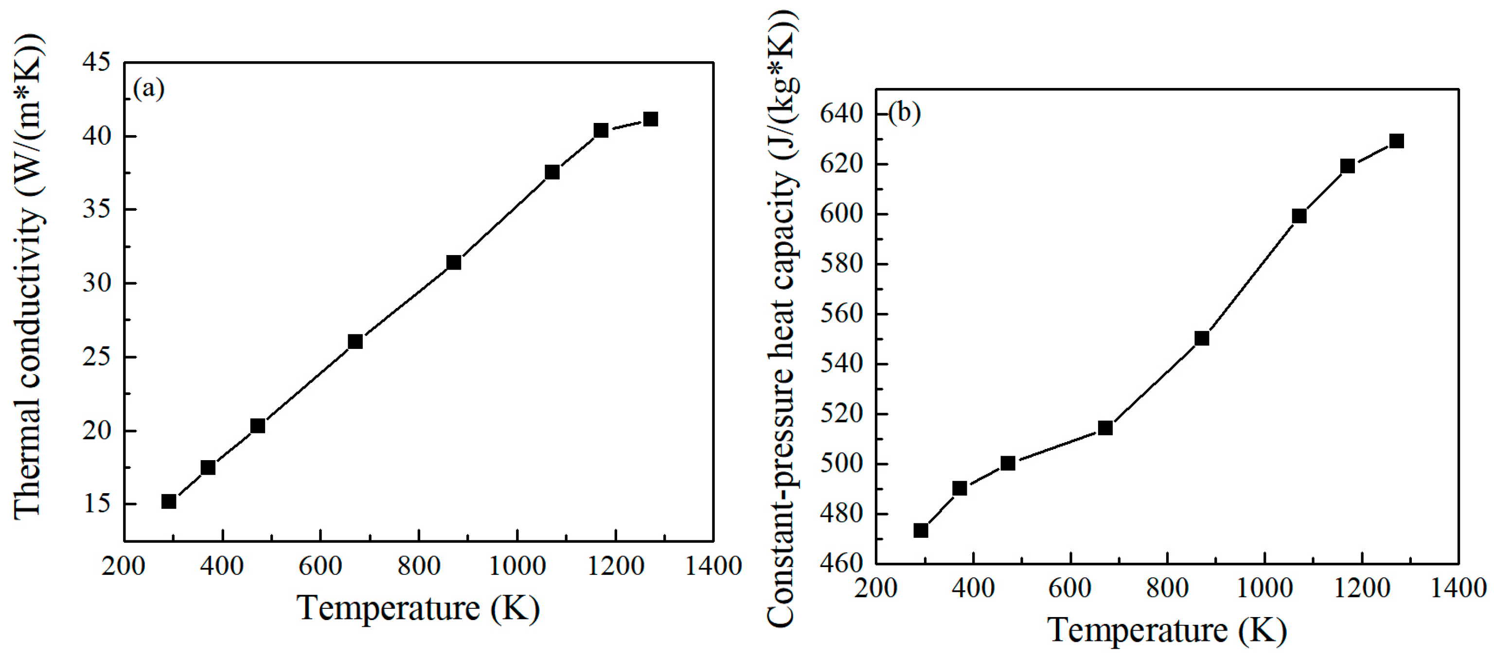
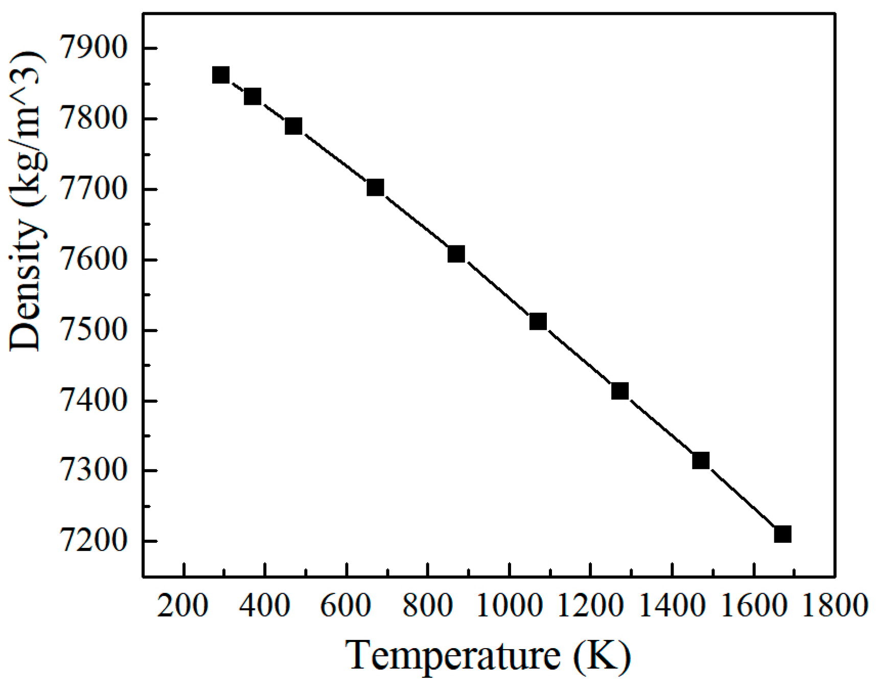
The surface processing of workpieces by hollow cathode electron beams involves continuous temperature variations, leading to corresponding changes in the thermophysical properties of the workpiece material, which are expressed as functions of temperature. The material used in the simulation experiment is 304 stainless steel, and the temperature-dependent functions of its thermophysical parameters, derived from empirical formulas [41], are given below.
Thermal conductivity (Figure 1a):
6.74 + 2.86 × 10 2 T     293 T 1200
Specific heat capacity at constant pressure (Figure 1b):
270 1.21 T + 2.15 × 10 2 T 2 7.51 × 10 5 T 3 + 8.14 × 10 8 T 4     293 T 310
109 + 2.57 T 6.53 × 10 3 T 2 + 7.79 × 10 6 T 3 4.17 × 10 9 T 4 + 8.09 × 10 13 T 5     310 T 1311
Density (Figure 2):
7945 1.98 × 10 1 T 3.71 × 10 4 T 2 + 2.21 × 10 7 T 3 5.13 × 10 11 T 4     293 T 1700
where temperature T is in units of kelvin (K), where 293 K corresponds to the initial temperature of 20 °C. For temperatures outside the ranges specified in the above functions, while the material remains in the solid state, the thermophysical parameters are calculated using their values at the upper temperature limit of the corresponding function.

2.4. Initial and Boundary Conditions

At the onset of irradiation, the workpiece surface has not yet been heated, and its temperature equals the ambient temperature. Thus, the initial condition is given by the following:
T t = T 0 t = 0
where T0 is the initial temperature of the processing zone, typically equal to the ambient temperature.
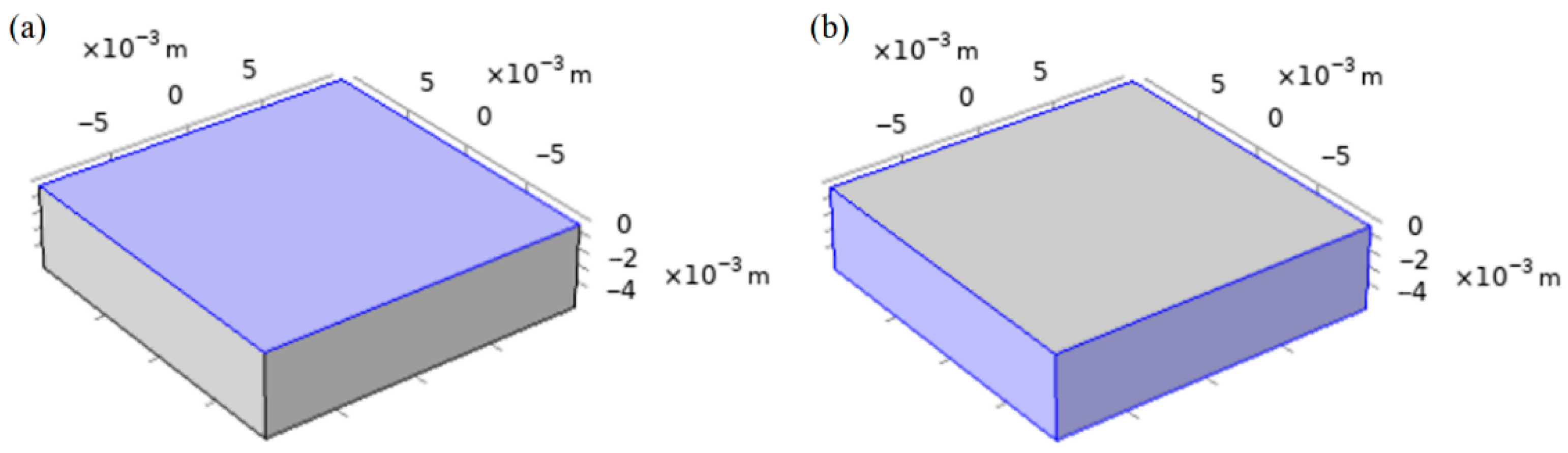
The workpiece dimensions (20 mm × 20 mm × 5 mm) are significantly larger than the diameter of the hollow cathode electron beam (3 mm). Moreover, the pulse duration of the hollow cathode electron beam is extremely short, resulting in minimal heat transfer. Therefore, except for the irradiated surface, the temperature at the workpiece boundaries can be considered equal to the surrounding temperature with negligible heat transfer. The geometric schematic of the two boundary conditions is illustrated in Figure 3.
  • Diffuse reflection condition: The electron beam-irradiated surface of the workpiece material is the heat transfer surface, containing a high-temperature distribution region with a significant temperature gradient relative to the surroundings. Thermal radiation from the surface to the environment must be considered [42]:
n λ T = ε σ 0 T 4 T 0 4
where T0 is the initial temperature, taken as 293 K, and T is the real-time temperature of the specimen surface. ε is the emissivity of the workpiece surface. σ0 is the Stefan–Boltzmann constant, typically taken as 5.67 × 10⁻⁸W−2K−4, and λ is the thermal conductivity.
2.
Thermal insulation condition: All other surfaces of the workpiece material are treated as thermally insulated, meaning their temperature remains equal to the ambient temperature with essentially no heat transfer or thermal radiation.

2.5. Mesh Generation

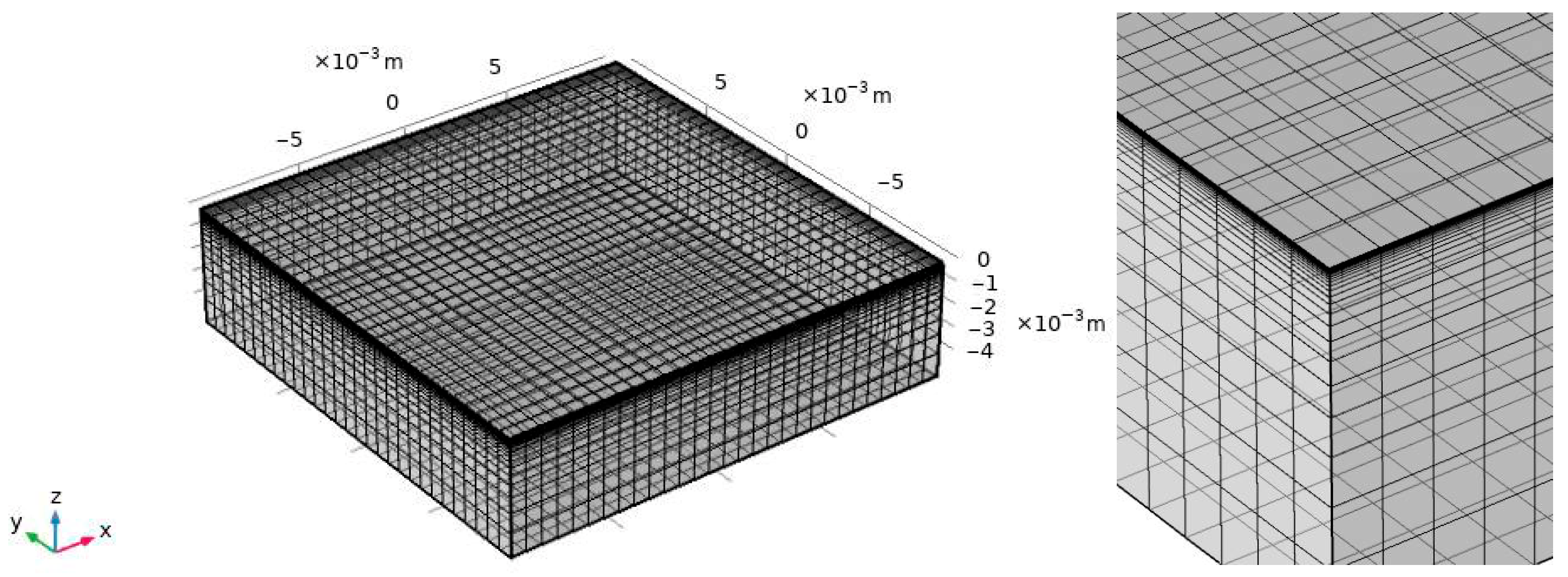
Considering the characteristics of hollow cathode electron beam surface heat treatment of workpiece materials, the remelted layer thickness is typically only on the order of tens of micrometers, while the heat-affected zone also extends within a range of several tens of micrometers. Therefore, the region of primary interest is confined to a very thin surface layer of the workpiece. To substantially reduce computational cost while enhancing calculation accuracy during the solution process, the mesh generation strategy involves refined treatment of the surface layer. Specifically, the mesh density is highest near the workpiece surface and gradually coarsens toward the substrate interior. The detailed distribution is illustrated in Figure 4 below: A predefined distribution type is applied along the depth direction, with an element aspect ratio of 0.001 and a total of 30 cells. In the length and width directions, the mesh is uniformly distributed.

2.6. Heat Source Model Input and Simulation Parameters

The heat source model for surface modification using a nanosecond pulsed hollow cathode electron beam is spatiotemporally variable. Moreover, the absorption of electron beam energy by the workpiece material surface is non-stationary and exhibits non-linear variation with depth. This section will analyze the heat source model input for hollow cathode electron beam surface modification in terms of spatial distribution, temporal characteristics, and energy absorption.
  • Spatial Variation
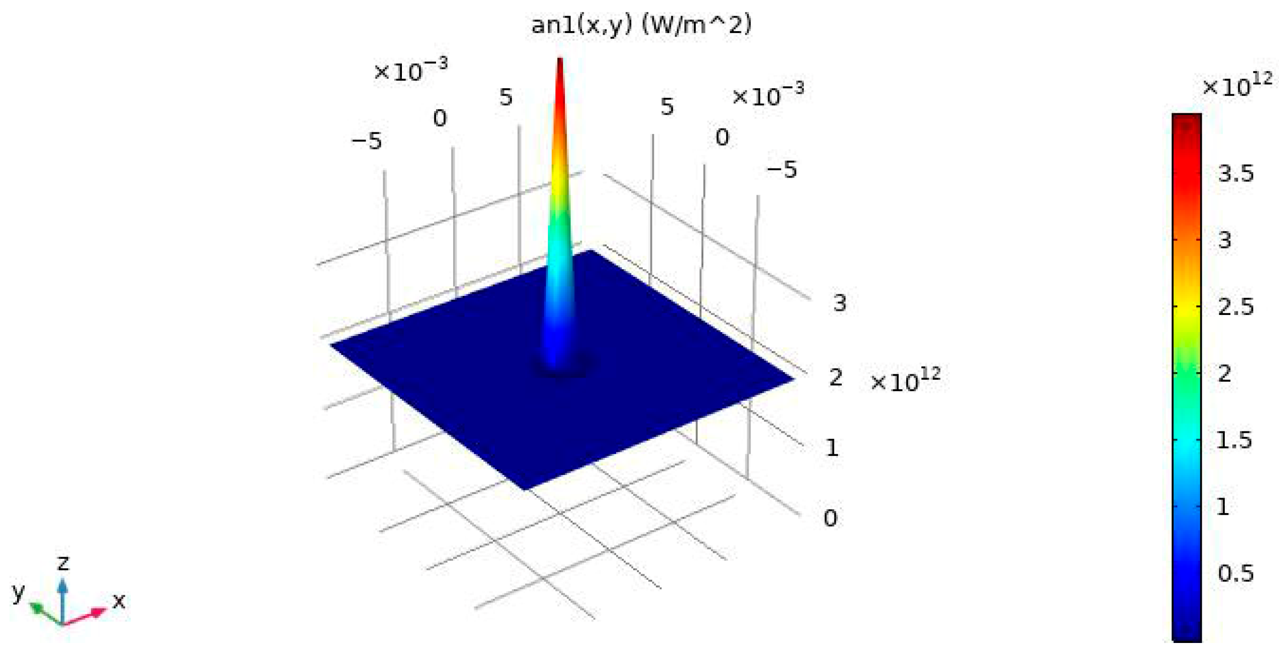
The thermal flux density of the hollow cathode electron beam is the highest at the center of the beam spot, decreases as the distance from the center increases, and reaches a minimum at the edge of the beam spot. The energy density distribution is symmetric about the beam axis, as was proposed in previous studies that the electron beam current generated by the hollow cathode discharge gradually changes from a random distribution in the central region to a Gaussian distribution [43]. This has also been confirmed by the actual processing morphology. Therefore, the spatial distribution of the electron beam thermal flux can be described by a Gaussian function that varies with the radius. The specific spatial distribution of the heat flux density is expressed as follows: based on the Gaussian function [44], the heat flux density is defined as follows:
q x , y = q m G x , y
where G x , y is a two-dimensional Gaussian distribution function, and q m is the maximum power at the center of the beam spot. Setting the irradiation center of the electron beam on the workpiece surface as the origin of the coordinate system, the Gaussian distribution function G x , y can be expressed as follows:
G x , y = 1 2 π σ 2 e x p x 2 + y 2 2 σ 2
where σ is the standard deviation of the Gaussian distribution function. With r0 = 3σ, according to empirical knowledge, the energy within the interval [−3σ, 3σ] accounts for 99.7% of the entire distribution. r0 represents the electron beam radius. Substituting σ in the formula with r0, the following expression is obtained:
G x , y = 4.5 π r 0 2 e x p 4.5 × x 2 + y 2 r 0 2
When temporal distribution is not considered, q m denotes the maximum power at the beam spot center, which can be expressed as follows:
q m = η U B I B
where η is the efficiency of converting electron beam energy into material thermal energy, UB is the applied voltage (i.e., the peak voltage of the electron beam), and IB is the peak current of the electron beam.
Based on the above derivation, the electron beam heat flux density on the workpiece surface can be expressed as follows:
q x , y = 4.5 η U B I B π r 0 2 e x p 4.5 × x 2 + y 2 r 0 2
The electron beam irradiates perpendicularly onto the upper surface of the workpiece, where its energy is absorbed. The kinetic energy of the electrons undergoes a series of transformations and is converted into thermal energy within the material. The Gaussian distribution of the electron beam heat flux density is illustrated in Figure 5.
2.
Temporal Variation
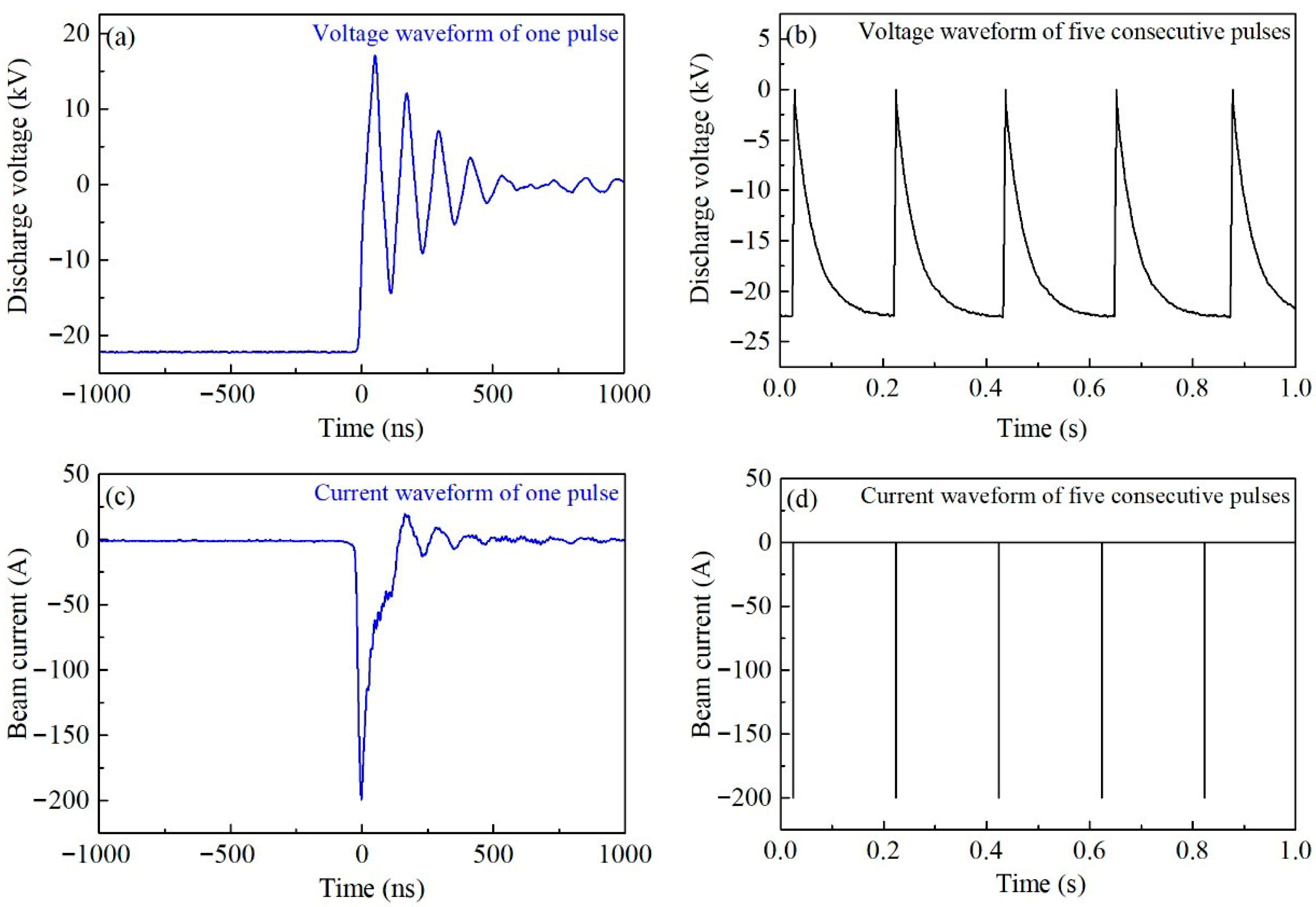
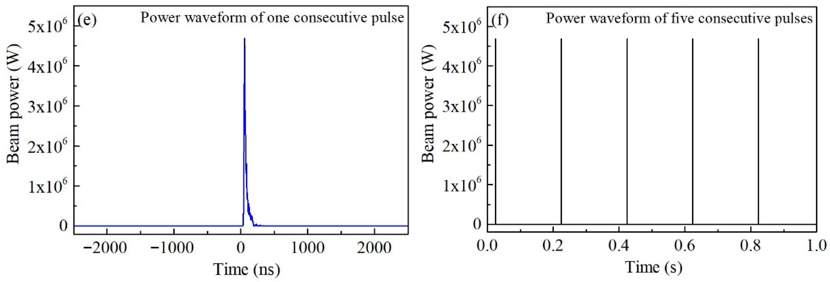
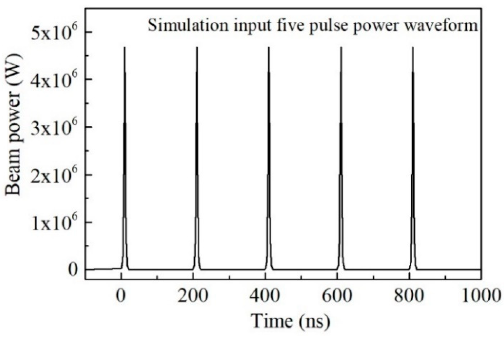
The hollow cathode electron beam is a pulsed electron beam, so the heat source input distribution function is not constant in the time domain but rather a periodic function that varies continuously with time. The experimentally measured electron beam pulse voltage, current, and power variations over time are shown in the figure below, where the power waveform is derived from the product of the corresponding instantaneous voltage and current values. Figure 6 illustrates the specific distributions for five consecutive pulses and a single pulse, respectively. As can be observed from the figure, the duration of the main pulse in a single electron beam pulse is approximately 100 ns, with a peak power of about 4.6 × 10⁶ W. The electron beam energy is highly compressed in time, yielding an instantaneous power density as high as ∼1011 W/m2 and a power rise rate of ∼1014 W/s. Throughout the time domain distribution, pulses occupy a relatively small proportion of the cycle but exhibit high peak values, which readily induce non-equilibrium states on the processed surface.
However, when incorporating temporal distribution into the heat source model input for thermal-stress simulation, computational constraints prevent direct input according to the actual time domain distribution; an equivalent shortening is required. Although a time step of 1 ns is suitable for simulating a nanosecond pulsed electron beam as a heat source, the actual electron beam operates at a pulse frequency of 5 Hz (period of 0.2 s). Within one period, this would require up to 2 × 10⁸ computational steps. With pulse counts potentially reaching 5000 in simulations, even 1000 steps could demand approximately 5 days of computation time, exceeding practical computational limits. Therefore, while preserving the waveform characteristics, the pulse duration and inter-pulse interval are equivalently shortened in the simulation. The pulse duration is set to 20 ns and the inter-pulse interval to 180 ns, with the pulse count also reduced proportionally. This yields the simulated input pulse power waveform shown in Figure 7, which retains the feature of a short pulse duty cycle while maintaining the original peak power value.
Incorporating the temporal distribution function, the electron beam heat flux density on the workpiece surface can be expressed as follows:
q x , y , t = 4.5 η U B I B π r 0 2 e x p 4.5 × x 2 + y 2 r 0 2 · i n t t
where i n t t is the normalized temporal distribution function. Since the peak power is already included, the i n t t function is input in the form of an interpolation function.
Under the current research objectives, the time-domain simplified treatment in this study remains reasonable. Target matching: The main objective of this study is to reveal the mechanisms (such as the grain refinement mechanism) and verify the rationality of the model structure (the spatial distribution of the heat source model and the energy deposition pattern), rather than precisely predicting absolute temperature/stress values. For mechanism research, the correctness of the trend is more important than numerical accuracy. Retention of key features: This simulation retains the core features that determine the thermal physical effects—small pulse duty cycle, peak power, and steep rising edge. These features determine extremely high heating/cooling rates (in the order of 1011 K/second), which is the physical basis for grain refinement. Effectiveness of relative comparison: This study focuses on the changing trends under different pulse frequencies, rather than the absolute values of individual conditions. When the time-domain compression ratio remains consistent, the conclusions of relative comparison are valid.
3.
Energy Absorption at the Workpiece Surface
Based on the analysis of the interaction process between the nanosecond pulsed hollow cathode electron beam and the workpiece material described above, it is concluded that the thickness of the layer absorbing electrons on the workpiece surface is on the order of micrometers. Next, the maximum penetration depth of electrons into the workpiece under specific parameters is calculated. The maximum vertical depth to which electrons penetrate the workpiece material, i.e., the electron range, follows a certain empirical rule. According to empirical formulas, the electron range is related to the accelerating voltage of the electron beam and the material density. The statistical relationship for electron range is given as follows [45]:
S 2.1 × 10 12 U B 2 ρ                 10   k V U B 100   k V
S 6.67 × 10 11 U B 5 / 3 ρ                 100   k V U B 1   M V
S 5.1 × 10 7 U B 0.26 ρ                     U B 1   M V
where S is the electron range in meters, UB is the accelerating voltage in volts, and ρ is the material density in g/cm3. For the workpiece material 304 stainless steel, as the electron beam voltage increases from 10 kV to 30 kV, the electron range increases from 0.27 μm to 2.43 μm.
Within the electron range, the deposited energy varies non-linearly with depth [45]. The functional relationship is expressed as follows:
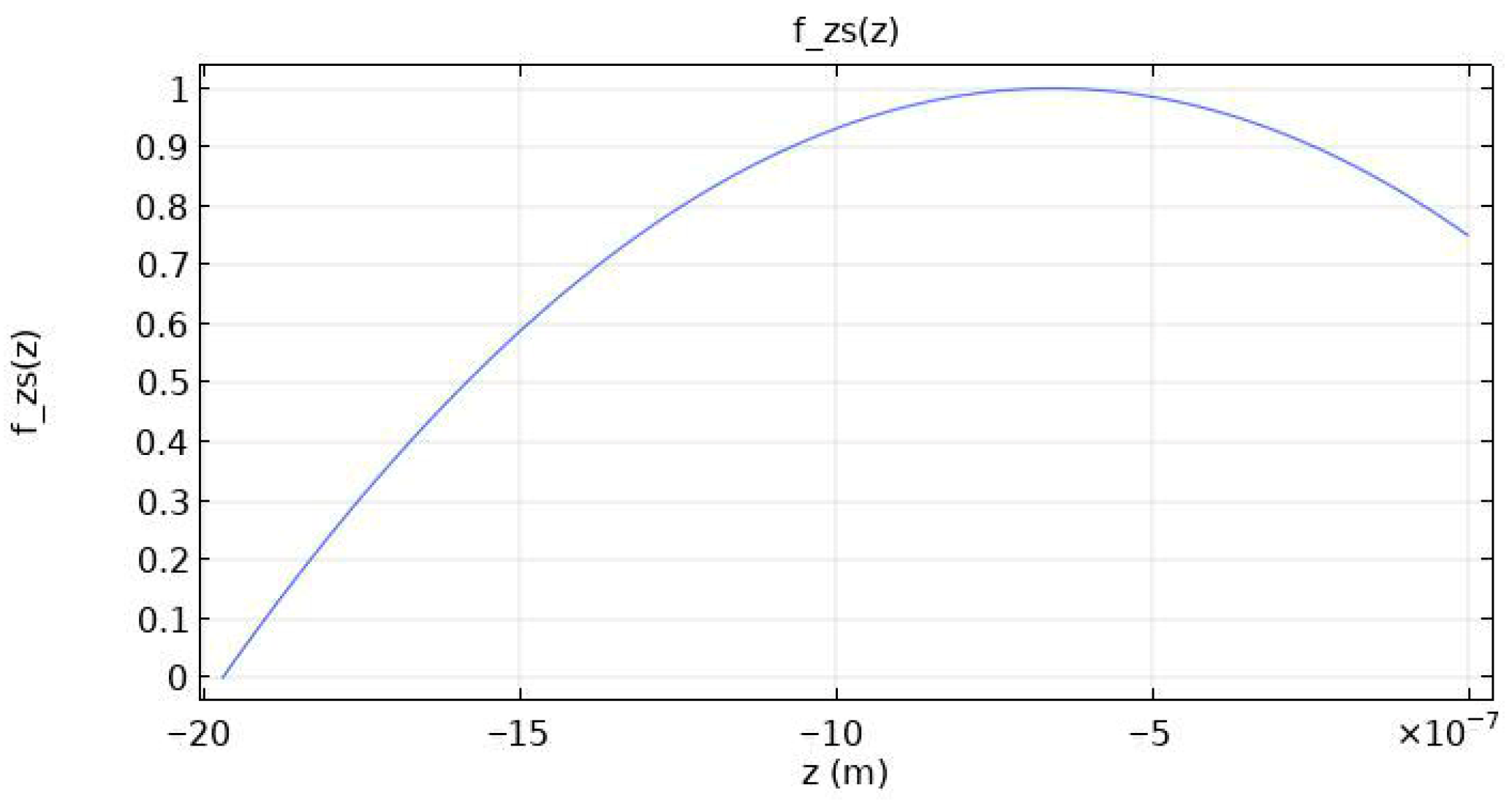
f _ z s z = 1 9 4 z s 1 3 2 s z 0
where f _ z s z represents the energy deposition coefficient at the corresponding depth, s is the range calculated from Equation (15) under the given electron beam parameters, and z is the coordinate along the depth direction. In the model, the coordinate origin is set at the irradiation center on the workpiece surface, so the range of electron deposition lies between −s and 0. The variation in the energy deposition coefficient with depth within the electron range is illustrated in Figure 8.
In summary, incorporating the spatial distribution, temporal variation, and energy absorption of the workpiece material, the heat source model function can be expressed as follows:
q ( x , y , z , t ) = 4.5 η U B I B π r 0 2 e x p 4.5 × x 2 + y 2 r 0 2 · i n t t · f z s z / s
where the unit of heat flux density q x , y , z , t is W/m3. After including the energy deposition function along the depth direction, the heat flux density transforms from a surface heat source distributed in the x and y directions to a volumetric heat source distributed in the x, y, and z directions. The heat source model for the nanosecond pulsed hollow cathode electron beam is thus a four-dimensional distribution function that varies simultaneously in three-dimensional space and time.
For the simulation of thermal and stress fields introduced by the hollow cathode electron beam during surface modification of two workpiece materials, the electron beam process parameters used are listed in Table 1. The number of electron beam pulses and the discharge voltage are treated as independent variables to analyze the variations in dynamic temperature and stress fields. The discharge voltage and beam current are kept consistent with the experimental values, while the pulse duration, interval time, and pulse count are selected according to the parameters of the simulation heat source model described above.

3. Results and Discussion

3.1. Dynamic Temperature/Stress Distribution in the Micron-Scale Surface Layer of the Irradiated Workpiece

3.1.1. Dynamic Variation in Maximum Temperature/Stress in the Micron-Scale Surface Layer of the Irradiated Workpiece

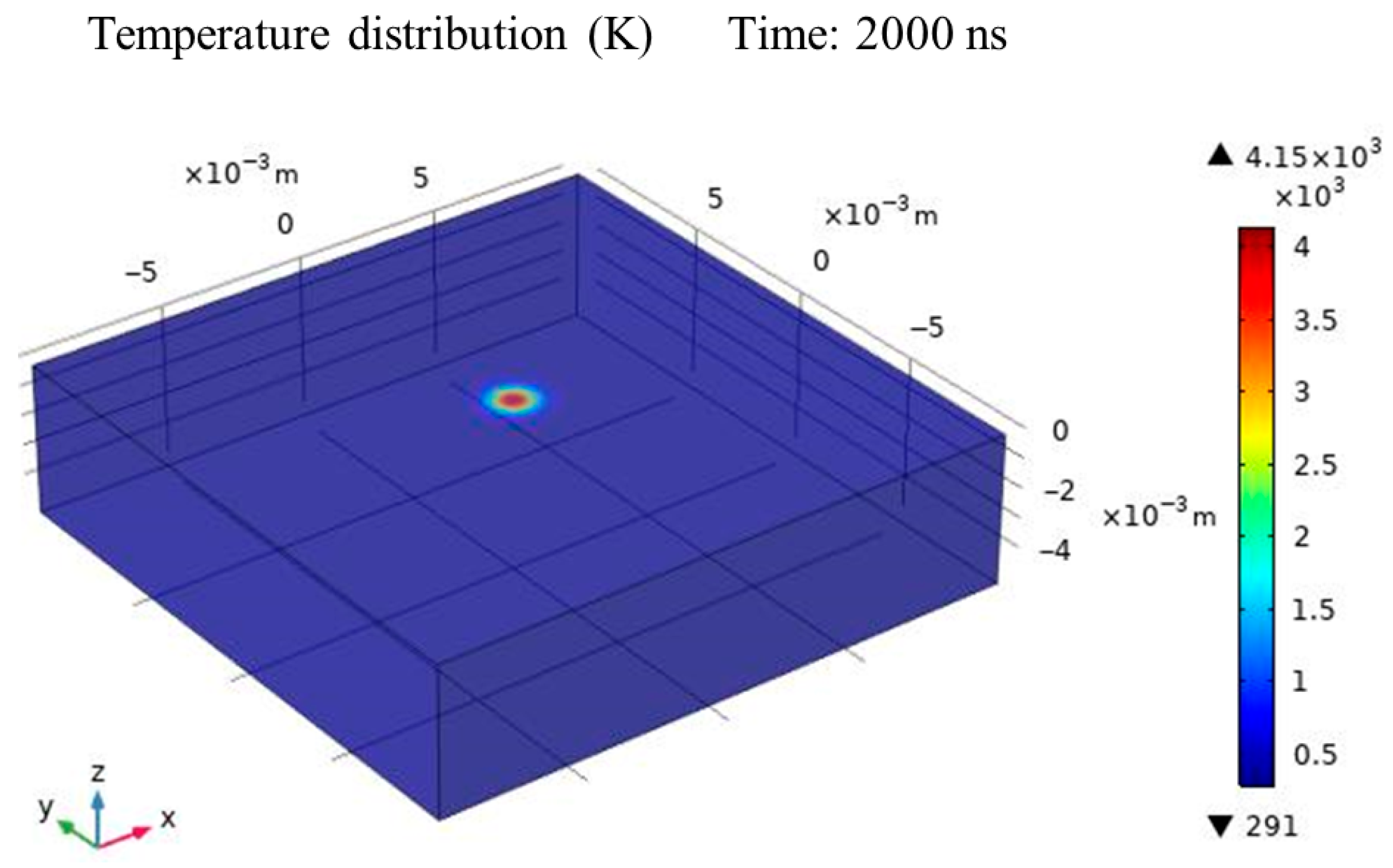
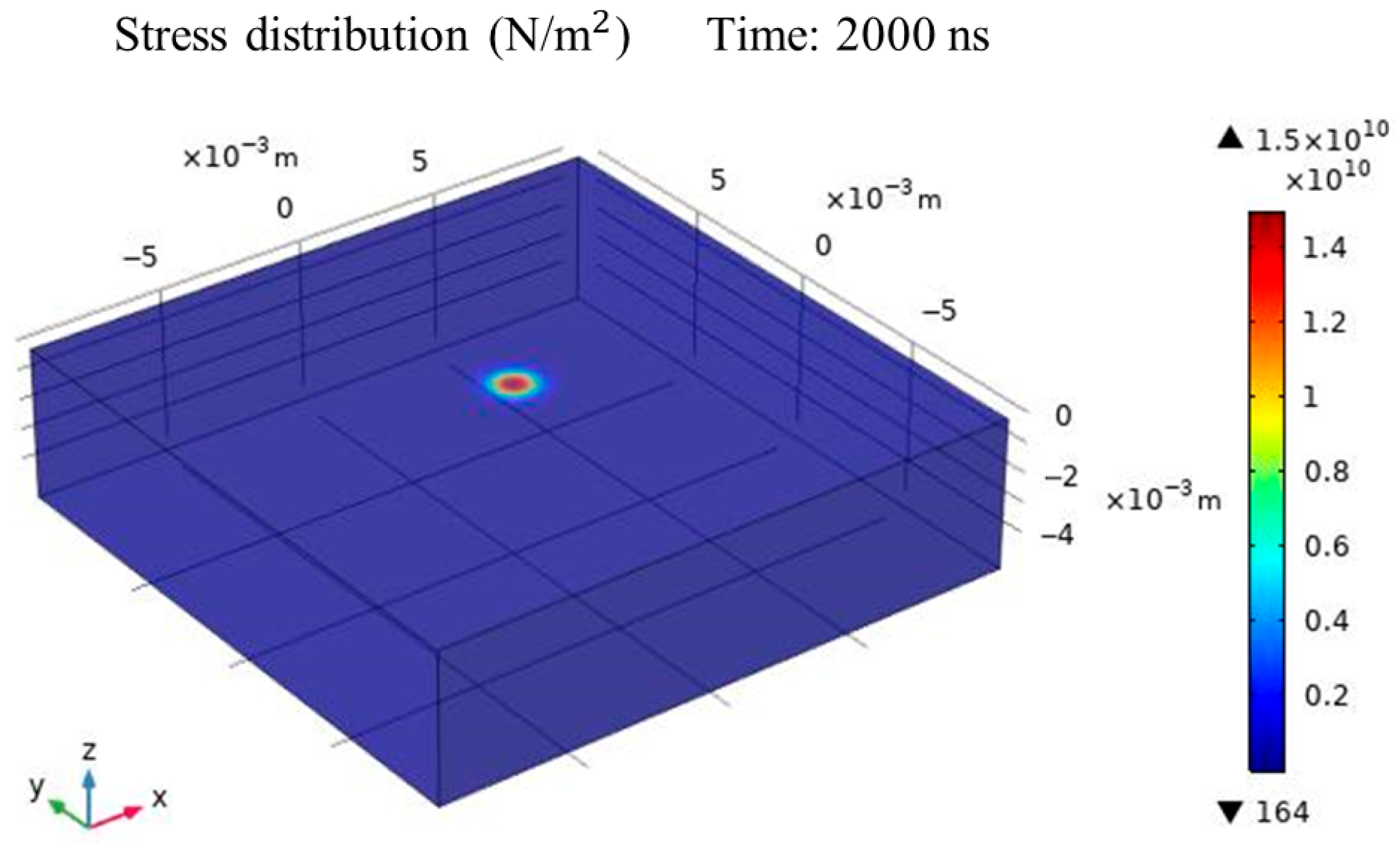
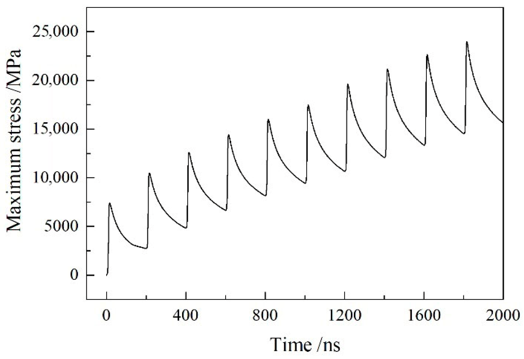
To assess the impact of nanosecond pulsed hollow cathode electron beam irradiation on the entire workpiece, Figure 9 shows the three-dimensional temperature distribution cloud map on a 304 stainless steel workpiece when the 10 electron beam pulses are completed (2000 ns) at a voltage of 22 kV. It should be noted that Figure 9 and Figure 10 represent the final state at the end of the treatment, while the dynamic evolution process of temperature/stress over time will be analyzed in detail in Figure 11, Figure 12, Figure 13 and Figure 14.
The isotherms exhibit a concentric ring distribution pattern in Figure 9. The high-temperature region reaching the melting point of 304 stainless steel (1670 °C) is confined to a very small area (approximately 1.5 mm in diameter), while the remaining regions of the substrate are essentially unaffected. This behavior is attributed to the characteristics of the nanosecond pulsed hollow cathode electron beam: although the beam spot diameter is 3 mm, the electron beam energy follows a Gaussian distribution in the radial direction, resulting in a remelted zone of about 1.5 mm. Moreover, the short pulse duration limits heat conduction from the surface, so the surrounding regions experience minimal thermal influence.
Similarly, Figure 9 shows the three-dimensional stress distribution over the entire 304 stainless steel workpiece at the end of 10 pulses (2000 ns) under 22 kV. High-stress regions are concentrated within a diameter of about 2 mm and coincide with the high-temperature remelted zone in the temperature contour map. The stress values in other regions of the workpiece substrate remain low and are largely unaffected. The nanosecond pulsed electron beam with high energy density deposits energy into a very small surface region within an extremely short time. During the pulse sequence, the temperature in the irradiated zone rises rapidly and then drops quickly after irradiation ceases. Over the course of 10 pulses, repeated thermal expansion and contraction of the irradiated zone generate a highly dynamic stress distribution, with stress magnitudes reaching the gigapascal (GPa) range, as illustrated in Figure 10. The ability of nanosecond pulsed hollow cathode electron beam irradiation to produce high temperatures and stresses within a localized micro-region makes it suitable for processing or modifying micro-scale components or precisely defined micro-areas on larger parts, without inducing significant effects in surrounding regions.
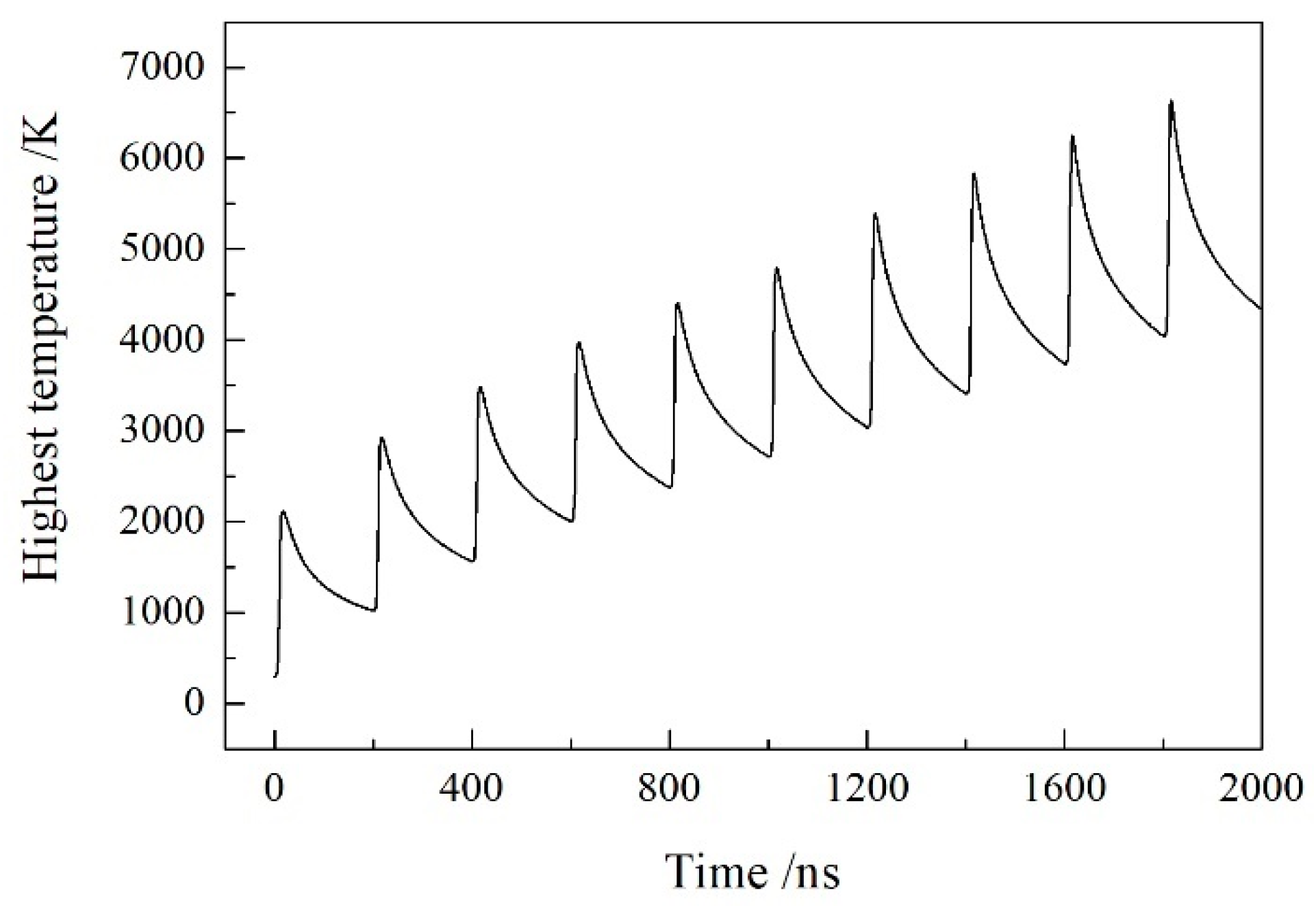
The following analysis addresses the influence of pulse number on temperature variation in the workpiece during electron beam irradiation. Figure 11 illustrates the evolution of the maximum temperature in the interaction zone of a 304 stainless steel workpiece over the course of 10 electron beam pulses. As shown in the figure, under constant pulse parameters, the temperature increase induced by a single pulse in the interaction zone rises with increasing pulse number. Moreover, the temperature increment after each pulse consistently exceeds the subsequent temperature decrease, indicating the presence of a heat accumulation effect in the interaction zone due to nanosecond pulsed hollow cathode electron beam irradiation. With the short pulse interval, an increase in pulse number leads to progressive heat accumulation in the surface interaction zone of the workpiece. This phenomenon of heat accumulation with increasing pulse count is also mentioned in the literature regarding the effect of high current pulsed electron beam treatment on the surface microstructure and corrosion resistance of Mg-4Sm alloy, where the electron beam operated at a pulse frequency of 0.1 Hz [46]. The nanosecond pulsed hollow cathode electron beam exhibits a high energy density, reaching up to 109 W/cm2, which results in extremely rapid heating of the workpiece surface. Within tens of nanoseconds, surface heating ceases and cooling begins. As evident from the figure, the cooling rate is significantly lower than the heating rate. Due to the short pulse interval, the temperature in the interaction zone does not return to its initial value before the next pulse arrives, leaving residual heat. This heat accumulation intensifies as the pulse number increases. Based on the temperature–time curve in the interaction zone, it can also be concluded that both the heating rate and cooling rate increase with the number of pulses.
Similarly, Figure 12 illustrates the variation in the maximum stress in the interaction zone of the 304 stainless steel workpiece over 10 electron beam pulses. Under identical pulse parameters for each pulse, the stress in the irradiated region rises rapidly within the initial tens of nanoseconds of each pulse as the temperature increases and subsequently decreases during the pulse interval as the temperature drops. As the pulsed electron beam continues to irradiate, the stress in the interaction zone undergoes repeated cyclic variations. With an increasing number of pulses, the stress variation range induced by each single pulse also expands. Both the stress increment during irradiation and the stress decrement during the subsequent interval increase, as detailed in Figure 12. Specifically, the stress increment per pulse rises from 7400 MPa for the first pulse to 9500 MPa for the tenth pulse, while the stress reduction during the interval increases from 4700 MPa to 8700 MPa over the same pulse sequence. The influence of pulse number on the stress reduction in the interaction zone is particularly pronounced. This trend in maximum stress variation closely follows the trend of maximum temperature variation in the interaction zone with increasing pulse number, effectively reproducing the temperature evolution pattern. Within tens of nanoseconds, the nanosecond pulsed hollow cathode electron beam delivers high energy density to the workpiece surface, causing the temperature to rise rapidly to approximately 2000 °C. A substantial temperature gradient forms between the irradiated region and the surrounding material. The greater the temperature difference, the higher the thermal stress generated in the interaction zone. Consequently, stress increases with rising temperature. Once irradiation ceases, the temperature drops promptly, the temperature gradient diminishes, and the stress in the irradiated region correspondingly decreases. As the pulsed electron beam continues to irradiate the surface, the stress in the interaction zone cyclically varies in synchronization with the temperature fluctuations.
The interaction of the nanosecond pulsed hollow cathode electron beam with the workpiece surface is highly localized, confined to a small region of approximately 1.5–2 mm, with minimal influence on the surrounding substrate. Within this interaction zone, extreme thermal and stress variations occur: temperature changes on the order of ~103 K and stress variations in the range of 103–104 MPa take place within tens of nanoseconds. Moreover, a pronounced heat accumulation effect is observed, which intensifies with increasing pulse count. Consequently, the rates of temperature and stress change also rise progressively with the number of pulses. This cumulative effect leads to a qualitative transformation in the surface modification outcome of the workpiece as the pulse number increases.
In the specific scenario where nanosecond pulsed hollow cathode electron beams interact with material, this assumption is reasonable and valid. The main reasons for this are as follows:
  • The highly concentrated energy distribution and Gaussian distribution characteristics: The core effects of surface modification (such as remelting, phase transformation, grain refinement, and high-stress plastic deformation) mainly occur in the region with the highest energy density. The temperature/stress changes in other regions of the substrate are very small and have little impact on the modification effect. Therefore, the extreme value characteristics of the central region directly determine the deepest and most intense changes in the modified layer and are the “decisive” indicators for evaluating the modification effect.
  • The strong correlation between temperature and stress: The maximum temperature gradient, highest temperature, and maximum thermal stress are spatially coincident. Therefore, tracking the extreme values of temperature and stress at the center point is essentially tracking the strongest signal of the thermodynamic behavior of the entire interaction zone. The variation pattern of this signal (such as heat accumulation, heating, and cooling rates) dominates the final modification result of the entire region.
  • Consistency in the trend of response changes: As long as the extreme points reflect the overall trend of change, using them as “representative indicators” to study the influence of parameters such as the number of pulses is effective.

3.1.2. Temperature/Stress Variation in the Cross-Sectional Remelted Layer of the Irradiated Workpiece

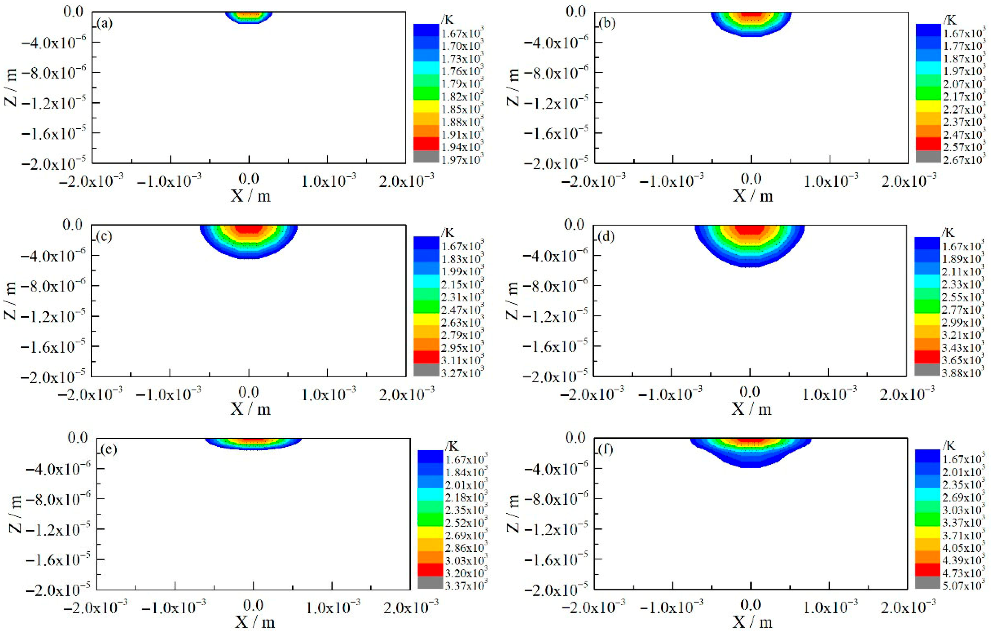
The following section focuses on the temperature variation in the cross-section of the irradiated workpiece, investigating the influence of pulse count on the remelted layer induced by the nanosecond pulsed electron beam. Figure 13 presents two-dimensional temperature contour plots of the longitudinal cross-section of a 304 stainless steel workpiece after irradiation with different pulse numbers, specifically showing regions where the temperature exceeds the melting point (i.e., the remelted zone). The temperature distribution in the longitudinal section exhibits a pattern in which the highest temperature is concentrated near the surface and gradually diffuses outward. For the same temperature difference, the spacing between isotherms becomes denser with increasing depth, indicating that the temperature gradient increases with depth. The maximum electron energy deposition occurs at approximately one-third of the electron range [45]. For an electron beam at 22 kV, the peak energy deposition is located around 0.46 μm below the surface. Therefore, the temperature distribution is characterized by a near-surface high-temperature region that diffuses outward. As shown in Figure 13a–d, as the pulse number increases, both the diameter and depth of the remelted zone expand, particularly in the depth direction, increasing from 1.6 μm at 3 pulses to 5.6 μm at 9 pulses. Furthermore, by comparing Figure 13e,f at the end of the pulse processing and before the start of the next pulse (including the time interval between two pulses) with Figure 13a,c just after the end of the pulse irradiation heating (excluding the interval time), it can be concluded that, immediately after the nanosecond pulsed electron beam stops irradiating and before it enters the pulse interval process, the diameter of the surface recrystallization layer is larger and the temperature is higher, but the thickness of the recrystallization layer is relatively smaller. This indicates that, during the tens of nanoseconds of electron beam irradiation heating, the surface hardly has time to transfer heat to the material substrate, and the heat transfer to the substrate mainly occurs after the irradiation ends and during the cooling process. Meanwhile, the absolute temperature values also rise, demonstrating the influence of heat accumulation, which intensifies with higher pulse counts. The thickness of the remelted layer varies from several hundred nanometers to several micrometers.
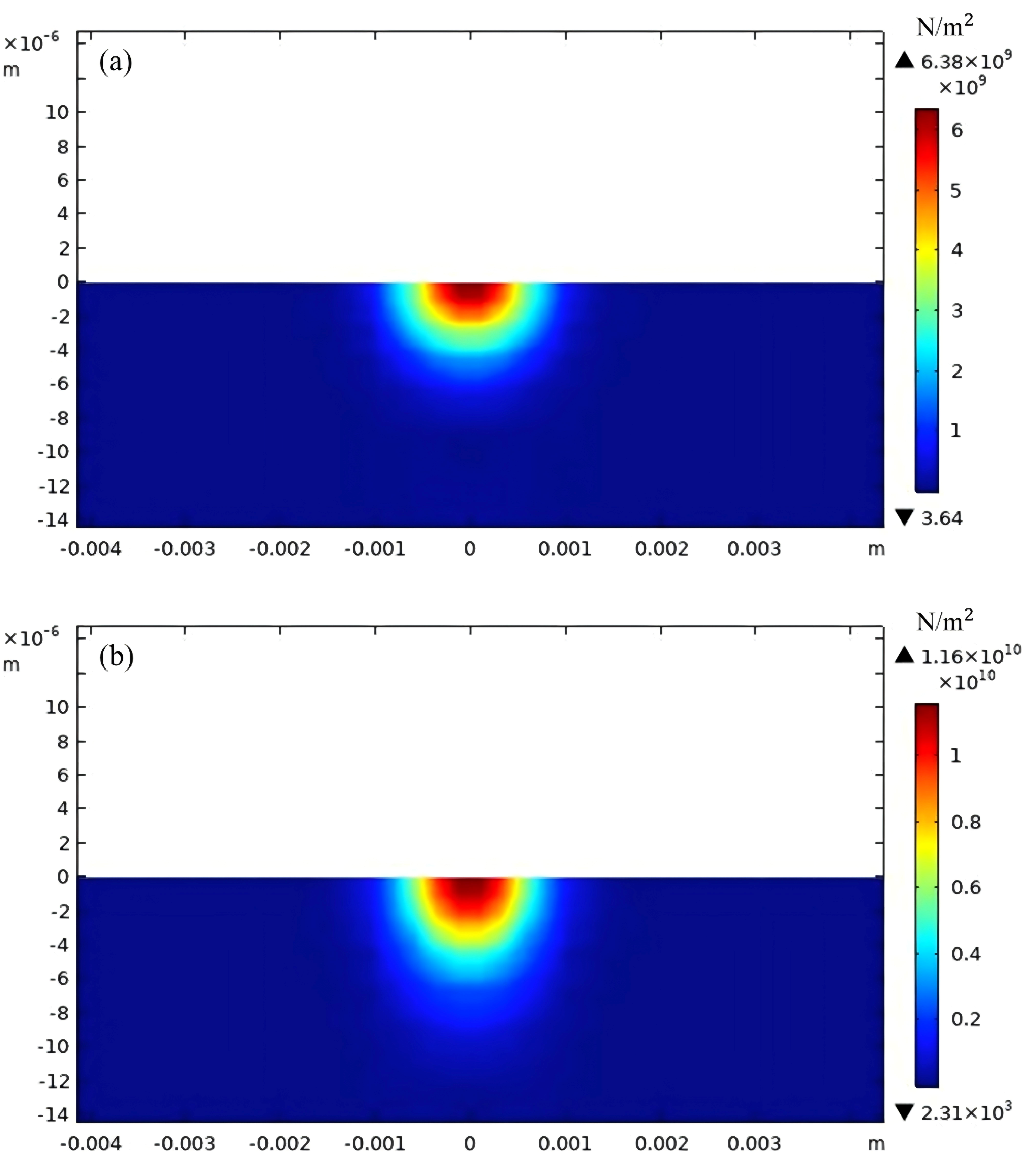
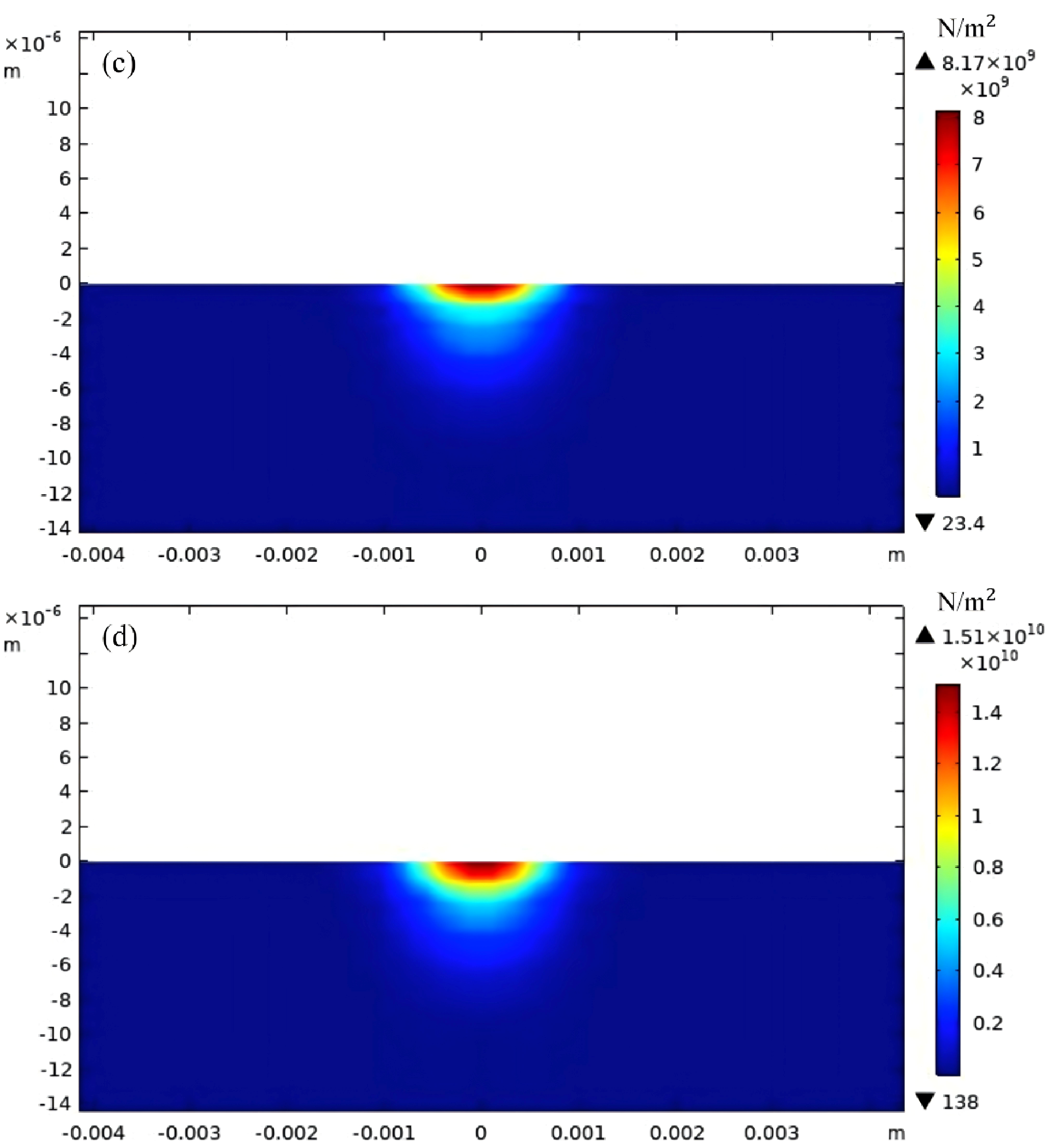
In parallel, to obtain a detailed distribution of stress within the irradiated surface region, especially along the depth direction, the two-dimensional stress contour plots of the workpiece after irradiation with different pulse numbers were analyzed, as shown in Figure 14. As the number of electron beam pulses increases, the region of concentrated stress gradually expands, particularly in the depth direction, extending from 6 μm at 3 pulses to 9 μm at 7 pulses. Comparing Figure 14a,b with Figure 14c,d, a similar situation was also observed in the high-stress areas of the cross-section. Just before the nanosecond pulse electron beam stops irradiating and enters the pulse interval, the diameter of the surface high-stress layer is larger, and the stress value is higher, but the thickness of the high-stress layer is relatively smaller. Moreover, the stress magnitude approximately doubles, indicating the presence of a stress accumulation effect. The stress distribution in the longitudinal section displays a pattern in which the highest stress is concentrated near the surface and diffuses outward in a roughly circular, contour-like manner, similar to the temperature distribution. Areas with higher temperatures exhibit more concentrated stress, while stress values progressively decrease with increasing depth. The high-stress region extends over a diameter of about 2 mm, while the stress in other areas of the workpiece remains very low and is essentially unaffected.

3.1.3. Variation in Heating/Cooling Rates of the Irradiated Workpiece Surface

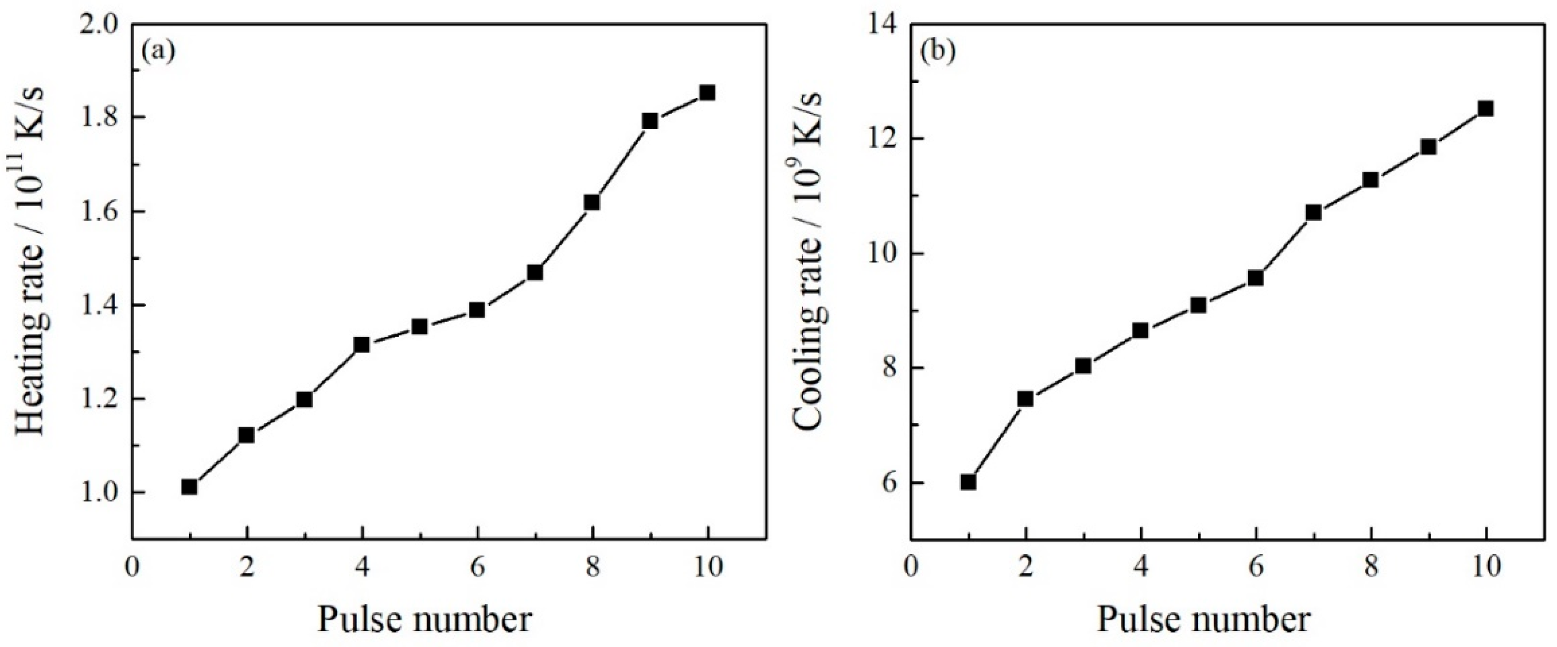
This section examines the heating and cooling rates induced by the nanosecond pulsed hollow cathode electron beam during surface irradiation, as these rates directly influence the evolution of micro–nano structures and properties of the irradiated surface and thus require focused investigation. Figure 15 presents the numerical relationship between heating/cooling rates and the number of pulses. As shown, both heating and cooling rates increase with the number of pulses. As previously established in the study of dynamic temperature/stress variations in the micron-scale surface layer, the irradiation of the nanosecond pulsed hollow cathode electron beam generates a heat accumulation effect in the interaction zone, and this accumulation intensifies with increasing pulse count. Under identical pulse parameters, the temperature change within the same time interval increases with the number of pulses, leading to the trend illustrated in Figure 15. Specifically, the heating rate rises from 1.01 × 10¹¹ K/s at 1 pulse to 1.85 × 10¹¹ K/s at 10 pulses, an increase of 83.2%. Meanwhile, the cooling rate increases from 6 × 10⁹ K/s to 12.5 × 10⁹ K/s, more than doubling. Pulse count significantly enhances both heating and cooling rates, with heat accumulation at higher pulse numbers having a more pronounced effect on the elevation of cooling rates. It can be inferred that, during nanosecond pulsed electron beam surface irradiation, the improvement in surface micro–nano structures and properties does not rely solely on the accumulation of pulses; more importantly, irradiation with a higher number of pulses induces qualitative changes in micro–nano structures and properties.
The heating rates of the nanosecond pulsed hollow cathode electron beam consistently remain on the order of 1011 K/s, while cooling rates range from 109 to 1010 K/s. In contrast, microsecond pulsed electron beams, depending on pulse duration, exhibit heating rates ranging from 108 to 109 K/s and cooling rates from 106 to 108 K/s [22,23]. Hence, the heating and cooling rates of the nanosecond pulsed hollow cathode electron beam exceed those of microsecond pulsed electron beams by one to two orders of magnitude. Consequently, the degree of grain refinement and plastic deformation induced by the two beam types is expected to differ significantly.

3.1.4. Comparison Between Simulation and Experimental Results

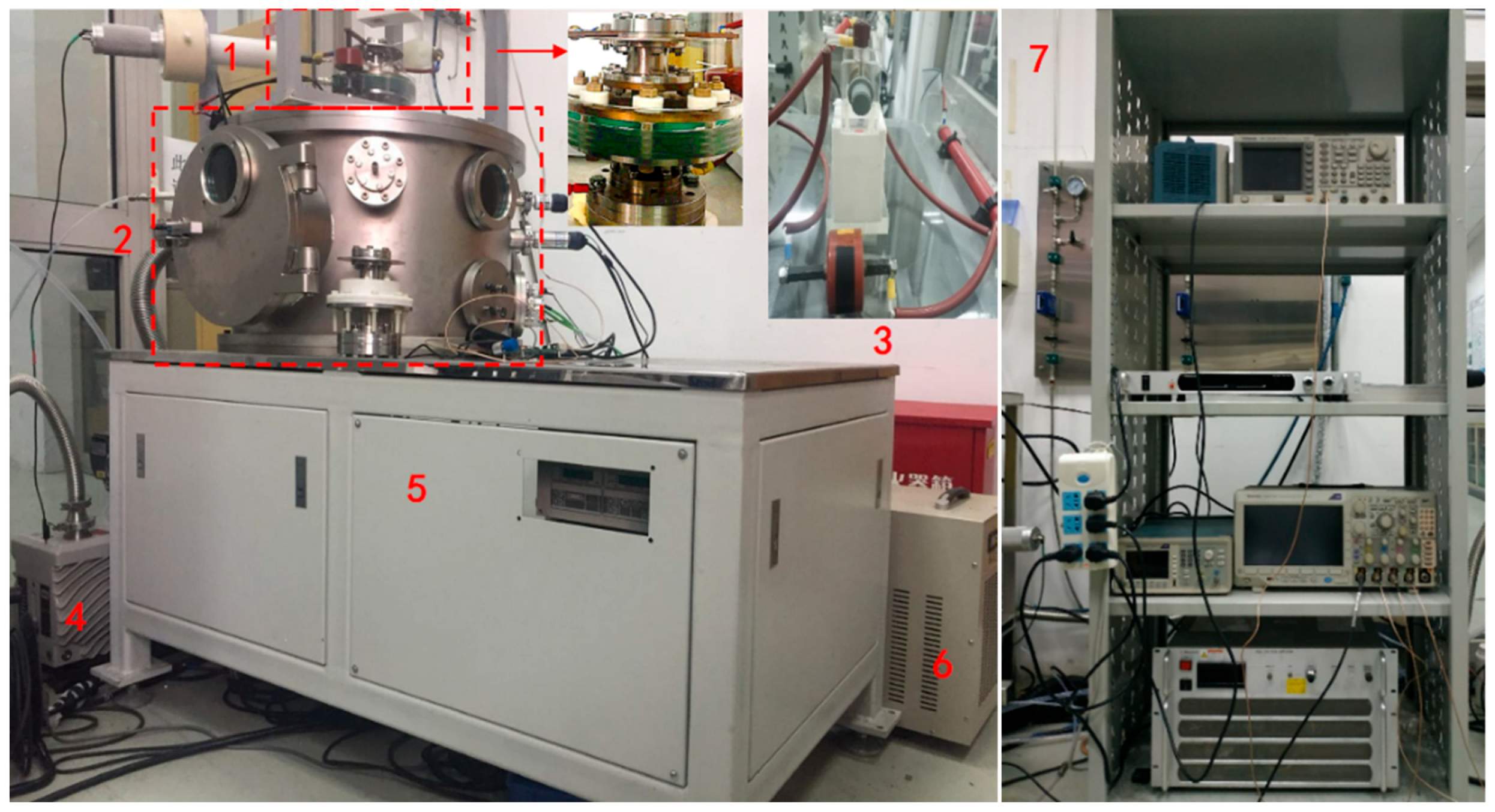
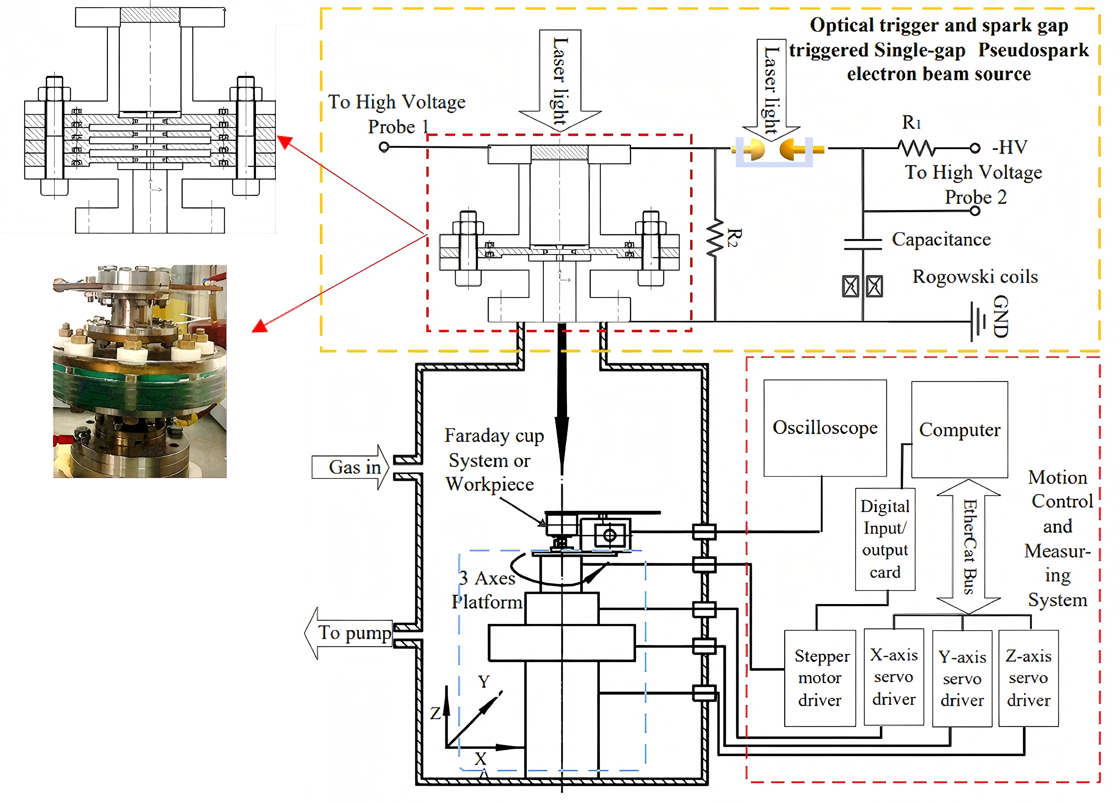
To validate the accuracy of the simulation model, a physical setup for the nanosecond pulsed hollow cathode electron beam processing of workpieces was constructed, as shown in Figure 16 and Figure 17. The system comprises a hollow cathode electron beam discharge device, a high-voltage pulse network, a vacuum chamber, a two-stage vacuum pumping system, and a worktable.
Hollow cathode discharge chamber: The hollow cathode electron beam discharge device is the core component of the system. It consists of a hollow cathode, an anode, and three intermediate electrodes, forming a multi-gap hollow cathode discharge. Insulating polytetrafluoroethylene (PTFE) spacers are placed between the cathode, intermediate electrodes, and anode. The cathode, intermediate electrodes, and anode are all made of conductive brass. A coaxial circular aperture with a diameter of 3 mm is machined through the center of the hollow cathode, intermediate electrodes, and anode to serve as a channel for electrons and positive ions. The hollow cathode cavity has a depth of 40 mm and a diameter of 40 mm. Two parallel capacitors are connected between the hollow cathode and the anode as energy-storage elements. A Rogowski coil is connected in series with the capacitors to measure the discharge current, while the discharge voltage is monitored using a high-voltage probe attached to the cathode.
High-voltage pulse network: The hollow cathode is connected to a high-voltage power supply through a 20 MΩ current-limiting resistor, which protects the power supply during the transient gas breakdown and discharge in the cavity. The resistor value is chosen according to the rated current of the high-voltage power supply.
Vacuum chamber: The vacuum chamber serves as the space for electron beam current measurement and surface modification experiments. It is equipped with a movable worktable and is connected to the anode of the hollow cathode discharge chamber. The two-stage vacuum pumping system consists of a mechanical pump and a molecular pump. Several ports are provided on the chamber for connecting mechanical and electrical devices, vacuum-level measurement instruments, and for optical observation. The experimental voltage and current parameters are consistent with those used in the simulations described earlier.
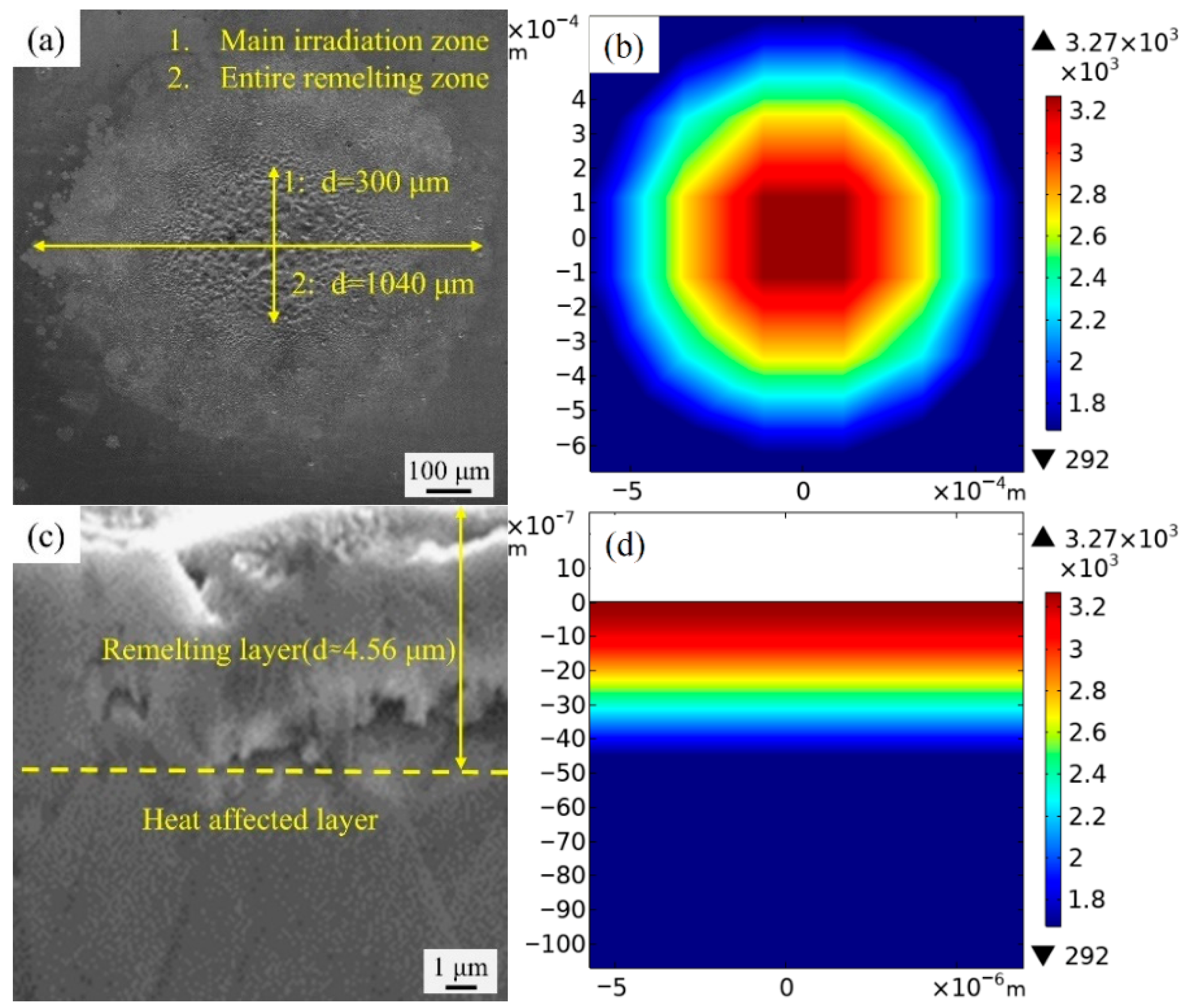
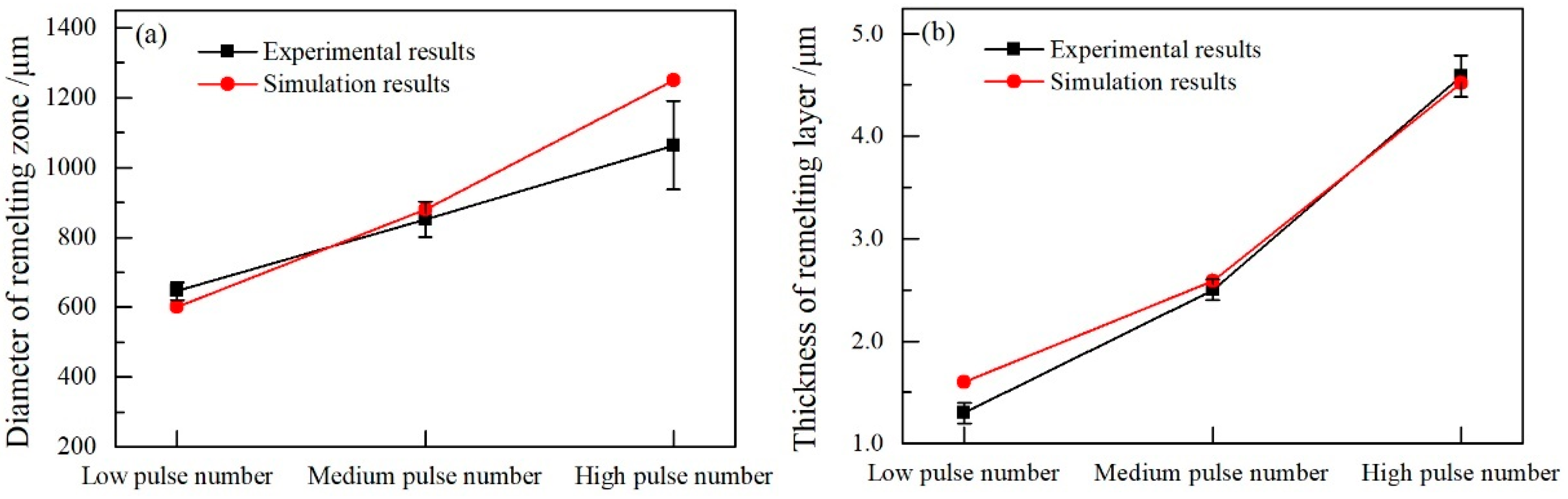
Figure 18 presents a comparison of the remelted zone diameter and remelted layer thickness obtained from experiments and simulations under a relatively high pulse count. As explained in Section 2.6 concerning the heat source model input, computational constraints required an equivalent shortening of the temporal profile in the simulation while preserving the waveform shape and duty cycle characteristics; consequently, the pulse count was correspondingly reduced. From the comparison in Figure 18a,b, it can be observed that the shape and size of the remelted zone agree well between experiment and simulation. Furthermore, the simulation predicts that the temperature increases from the irradiation edge toward the beam center, which aligns with the experimental trend where the degree of remelting increases from the periphery to the center. Figure 18c,d provide a quantitative comparison of the remelted layer thickness, both indicating a thickness of approximately 4.5 μm. Based on the agreement in the remelted zone shape, size, and layer thickness, the rationality of the simulation model is confirmed. A comparison of the simulated and experimental remelted zone diameters and remelted layer thicknesses under different electron beam pulse counts is shown in Figure 19. Under low, medium, and high pulse counts, the simulated values for both remelted zone diameter and layer thickness show good consistency with the experimental data. Therefore, the established heat source model for the nanosecond pulsed hollow cathode electron beam used in surface modification is validated as reasonable.
The quantitative error analysis is as follows:
  • Quantitative error analysis of the remelted zone diameter
Based on the experimental and simulation data of different pulse numbers in Figure 17, we calculated the absolute error and relative percentage error of the remelted zone diameter as shown in Table 2:
2.
Quantitative error analysis of the remelted layer thickness
Similarly, we conducted an error analysis on the remelted layer thickness (Table 3):
3.
Statistical error analysis
To further evaluate the overall prediction accuracy of the model, we calculated the following statistical indicators: average relative error of the remelted zone diameter: 4.5%; maximum relative error of the remelted zone diameter: 5.0%; average relative error of the remelted layer thickness: 4.6% (excluding the 0% error point)/3.5% when considering the 0% point; maximum relative error of the remelted layer thickness: 7.1%.
4.
Error source analysis
All the above errors are within the acceptable engineering range (<10%), which proves that the established heat source model has good predictive ability. Possible sources of error include the following:
Approximate treatment of material thermal physical parameters: The thermal physical parameters of 304 stainless steel used in the simulation (Equations (4)–(6)) are obtained based on empirical formulas, which may have slight differences from the actual batch characteristics of the material. Especially in the temperature range close to the melting point, the thermal conductivity and specific heat capacity of the material change dramatically, and the accuracy of the empirical formula may decrease.
Simplification of latent heat treatment: Although the model considers the latent heat of melting (Equation (3)), the method of equivalent treatment of latent heat to specific heat capacity is an engineering approximation, which may have a slight impact on the precise position of the phase change interface.
Equivalent shortening of the heat source time domain distribution: As described in Section 2.6, due to the limitations of the calculation conditions, we shortened the pulse duration while maintaining the waveform characteristics. Although this time-domain compression retains the characteristic of a small pulse ratio, it may have a slight impact on the details of heat diffusion, especially on parameters sensitive to heat conduction time, such as the remelted layer thickness.
Idealization of energy deposition distribution: In the model, it is assumed that the electron energy deposition follows an ideal Gaussian distribution (Equation (11)) and a specific depth distribution law (Equation (16)). However, in the actual discharge process, due to the complexity of the hollow cathode effect, the energy distribution may have slight asymmetry.
Based on the above quantitative error analysis, the prediction errors of all key indicators (remelted zone diameter and remelted layer thickness) are controlled within 7.1%, with an average error of less than 5%. This level of accuracy is acceptable and has good engineering practicality for a heat source model involving ultrafast thermomechanical coupling, phase change, and other complex multi-physics processes in nanosecond pulsed electron beam surface modification. Therefore, the quantitative error analysis further confirms the rationality and reliability of the thermal source model of nanosecond pulsed hollow cathode electron beam surface modification established in this paper.

3.2. Influence of Thermal and Stress Effects on Surface Micromorphology and Grain Refinement of the Irradiated Workpiece

3.2.1. Role of Thermal and Stress Effects in the Evolution of Workpiece Surface Micromorphology

This subsection focuses on analyzing the influence of the thermal and stress fields introduced by electron beam irradiation on the surface topographic profile of the 304 stainless steel workpiece. As indicated in previous sections, the surface micromorphology of the 304 stainless steel workpiece varies significantly under different electron beam pulse counts. However, a quantitative evaluation of these variations has been lacking, and the numerical relationship between the corresponding thermal/stress conditions under specific beam parameters and the resulting topographic profiles remains unclear. This subsection addresses these aspects in detail.
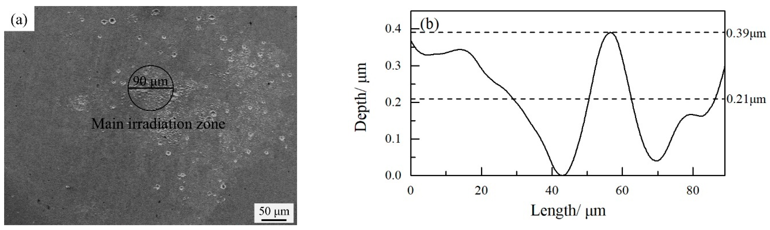
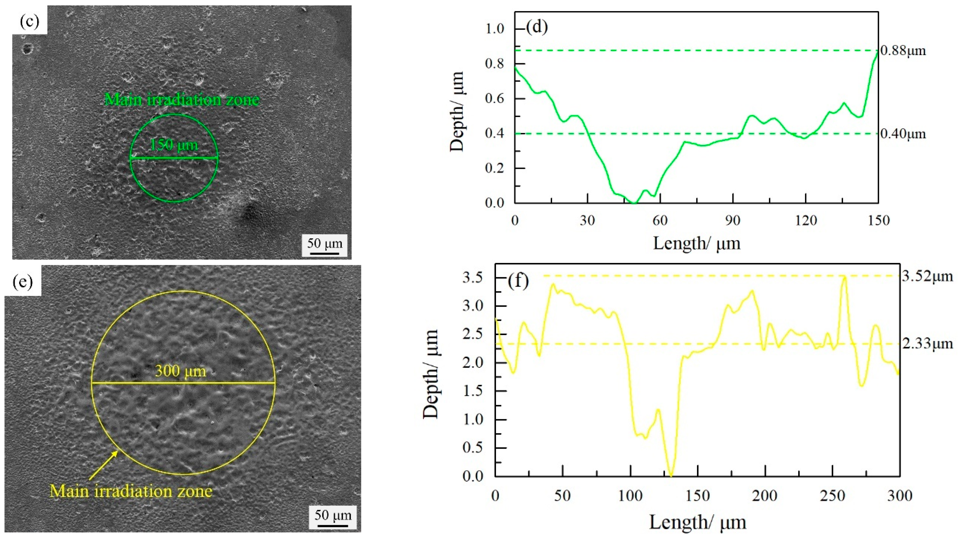
First, a quantitative assessment of the surface micromorphology of the 304 stainless steel workpiece is performed. Using confocal microscopy, the height variation profiles of the main irradiated zones under different pulse counts are obtained, as shown in Figure 20. Both the diameter of the main irradiated zone and the height variation in the topographic profile increase with the number of electron beam pulses. The diameter of the main irradiated zone increases from approximately 90 μm under low pulse counts to about 300 μm under high pulse counts, while the average height difference rises from 0.21 μm to 2.33 μm. As the pulse count increases, heat accumulation becomes more pronounced, leading to expansion of the heat-affected region both radially and in depth. Consequently, both the diameter and depth of the main irradiated zone gradually increase, and the depth of cratering or material ejection also becomes more significant. The rise time of the hollow cathode nanosecond pulsed electron beam is around 10 ns, with a pulse duration of approximately 100 ns. During this period, temperatures reach several thousand kelvins and stresses reach several gigapascals. Thus, the rates of temperature and stress change in the main irradiated zone are extremely high, placing the surface in a highly non-equilibrium state. Under the influence of such intense thermal and stress gradients, the surface undergoes rapid flow and plastic deformation, resulting in pronounced topographic height differences. Moreover, these height differences increase with the magnitude of the induced stress.
To investigate the numerical relationship between the temperature/stress introduced by electron beam irradiation and the resulting changes in surface morphology, the product of the average height difference in the topographic profile and the diameter of the main irradiated zone on the 304 stainless steel surface under different pulse counts is used as a quantitative metric for evaluating surface morphology. We chose “the product of the irradiation zone diameter and the height difference” as the quantitative indicator for microscopic morphology, based on the particularity of the research object. The surface morphology of nanosecond pulsed hollow cathode electron beam processing has the characteristics of high localization and non-uniform distribution, which is fundamentally different from the surface of traditional mechanical processing or overall heat treatment. This “local island-like” morphological feature makes traditional surface roughness parameters (Ra, Rz, etc.) face the following problems: sampling length is difficult to determine: the roughness parameters require the sampling length to include multiple characteristic periods, but in this study, the size of the morphology feature area (~300 μm) is comparable to the size of the feature itself, making it difficult to meet the statistical requirements; background interference: if the sampling area contains unprocessed base material, the roughness value will be “diluted” and cannot accurately reflect the actual degree of morphology change in the processing area. The product of the irradiation zone diameter and the average height difference is a comprehensive indicator of morphology change. Approximately characterizes the “overall volume effect” of morphology change, comprehensively considering the changes in both the lateral and longitudinal dimensions, and is used to evaluate the overall degree of morphology evolution brought about by an increase in pulse frequency.
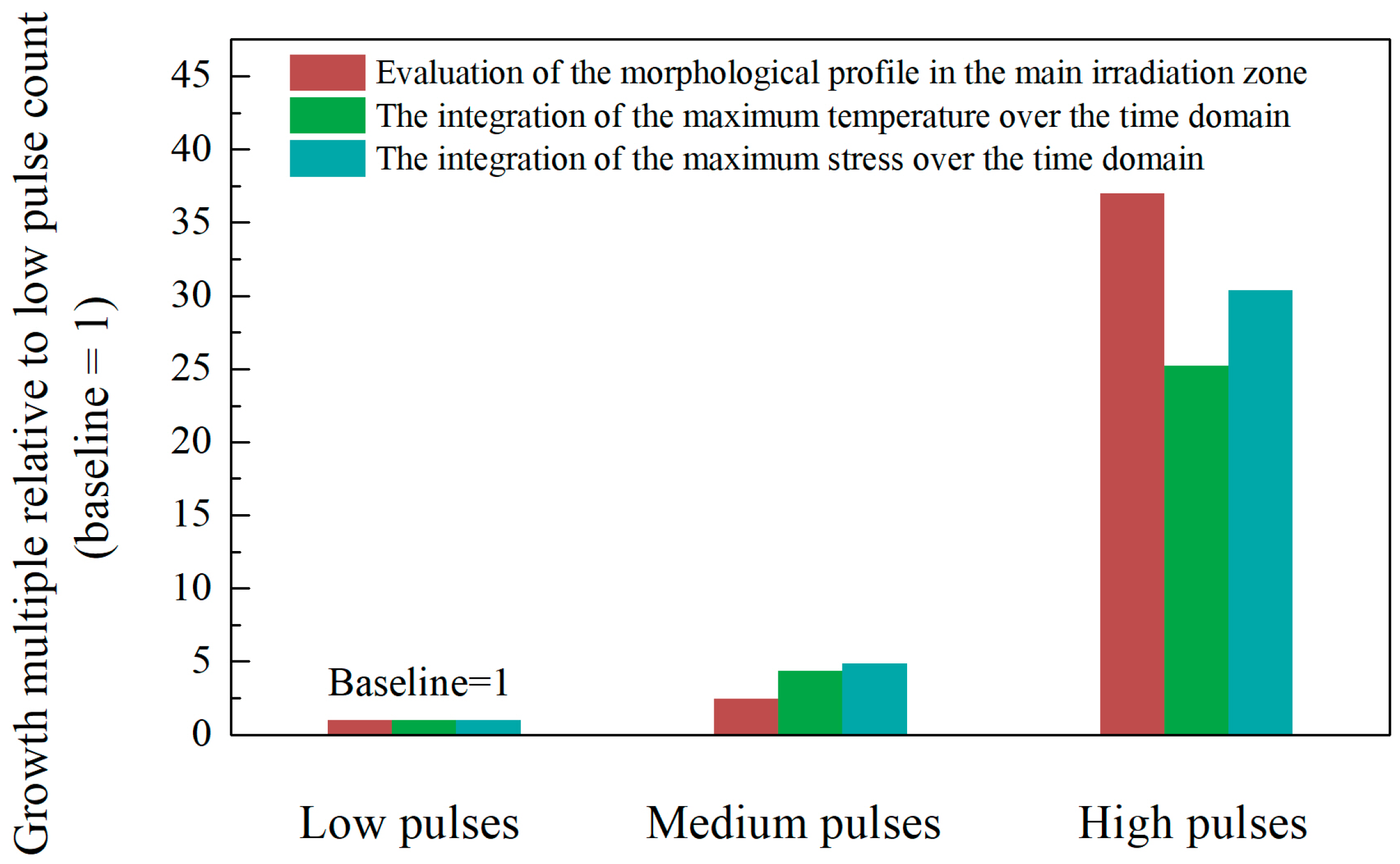
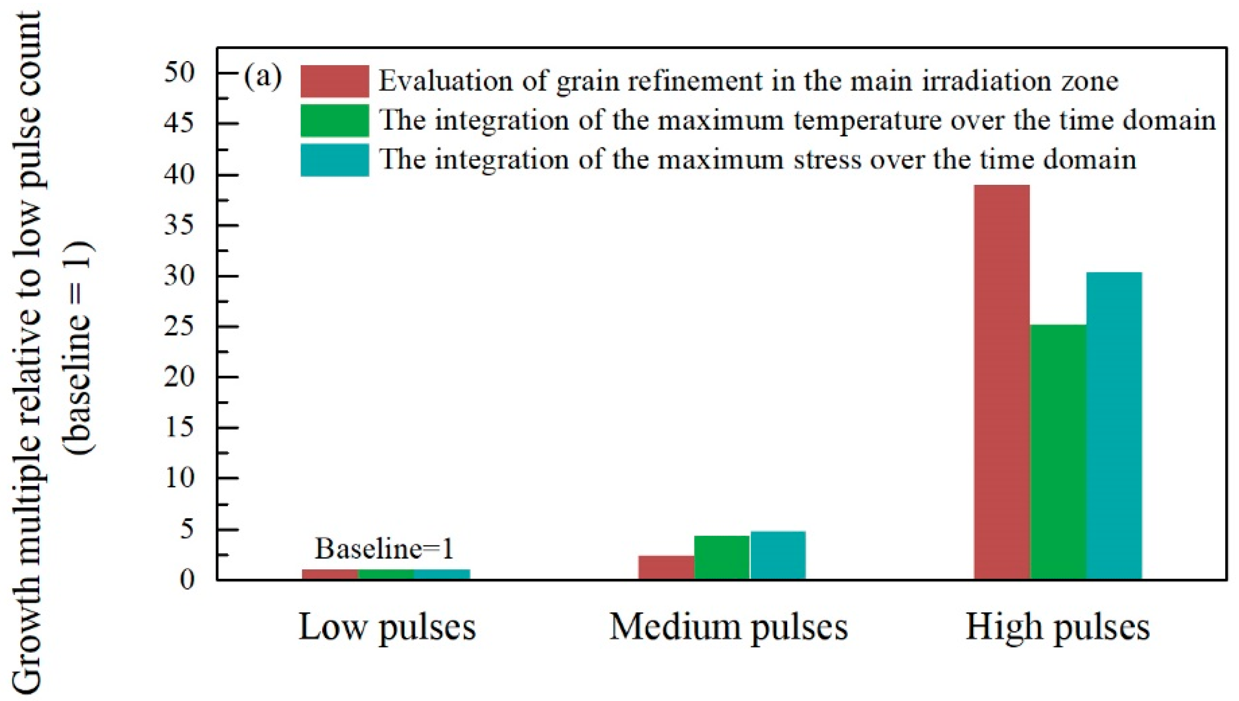
Meanwhile, the time integrals of the maximum temperature and maximum stress are adopted as numerical representations of the thermal and stress conditions in the main irradiated zone. Since the maximum temperature and stress occur near the irradiation center, they can reasonably represent the overall conditions in the primary interaction zone to a certain extent. Growth multiples of surface morphological profile, maximum temperature, and maximum stress under different pulse counts relative to a low pulse count (baseline = 1) are presented in Figure 21. Using the values of morphology, temperature, and stress obtained under low pulse counts as a baseline, the relative increases under medium and high pulse counts are expressed as multiples of the baseline. As shown in the figure, the growth multiples for morphology, temperature, and stress under high pulse counts are significantly larger than those under medium pulse counts. Specifically, the growth of the morphology is 36 times, which is greater than the growth of temperature by 24 times and the growth of stress by 29 times. This indicates that both temperature and stress contribute to the topographic evolution, and the compressive effect induced by stress plays a more dominant role than the filling effect resulting from increased pulse counts on crater morphology.
In summary, through the quantitative evaluation of the micromorphological profile of the 304 stainless steel workpiece surface under different electron beam pulse counts, and the investigation of its numerical relationship with the corresponding temperature and stress under each pulse condition, it is concluded that on the workpiece surface irradiated by the hollow cathode nanosecond pulsed electron beam, thermal and stress effects lead to a distinct outcome: as the pulse count increases, the irradiated surface does not become smoother; instead, it develops more pronounced micro-topographic features with larger height differences, consisting of protruding and recessed structures. Moreover, with increasing pulse counts, the lateral dimensions of these micro-features expand, while individual protrusions and depressions exhibit relatively flat local surfaces. The hollow cathode nanosecond pulsed electron beam has a rise time of approximately 10 ns and a pulse duration of about 100 ns. During this interval, temperatures reach several thousand kelvins and stresses reach several gigapascals, resulting in extremely high rates of temperature and stress change in the primary irradiation zone. This places the surface in a highly non-equilibrium state, where intense thermal gradients and stress induce rapid flow and plastic deformation, generating significant topographic height differences. The extent of this compressive deformation increases with the number of pulses and outweighs any filling effect that additional pulses might have on crater morphology. This behavior differs from the trend observed with microsecond high-current pulsed electron beams, where increased pulse counts primarily enhance the filling of surface craters more than the compressive effect of stress, thereby improving surface smoothness and flatness.

3.2.2. Influence of Thermal and Stress on Grain Refinement of the Workpiece Surface

This section primarily analyzes the influence of the thermal/stress fields introduced by nanosecond pulsed hollow cathode electron beam irradiation on grain refinement in the surface layer of a 304 stainless steel workpiece. Within the surface temperature exceeding the melting point, both the rapid temperature variation and high stress levels facilitate grain refinement. The fast-heating process characteristic of hollow cathode electron beam surface treatment, especially with a pulse rise time of ~10 ns, generates significant superheating on the workpiece surface, leading to the formation of a large number of nucleation sites. Furthermore, the short pulse duration (~100 ns) and the subsequent rapid cooling rate limit the time available for grain growth, thereby refining the original coarse grains. The high stress generated on the workpiece surface induces plastic deformation, producing slip bands, dislocations, and sub-grains, which also contribute to the refinement of coarse grains. In this section, the grain size distribution on the surface of 304 stainless steel irradiated with different electron beam pulses is statistically analyzed, and the quantitative relationship between the temperature/stress introduced by the electron beam and surface grain refinement is investigated.
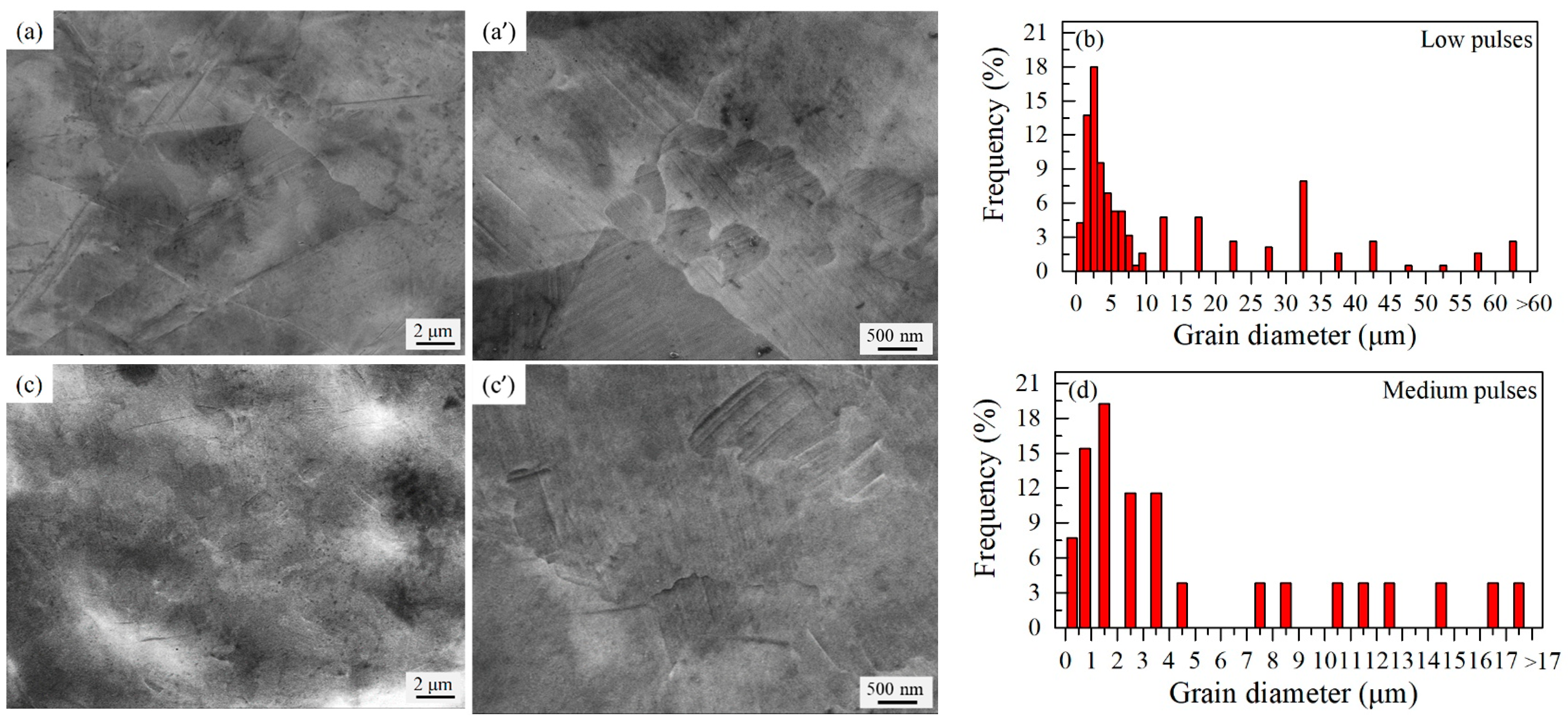
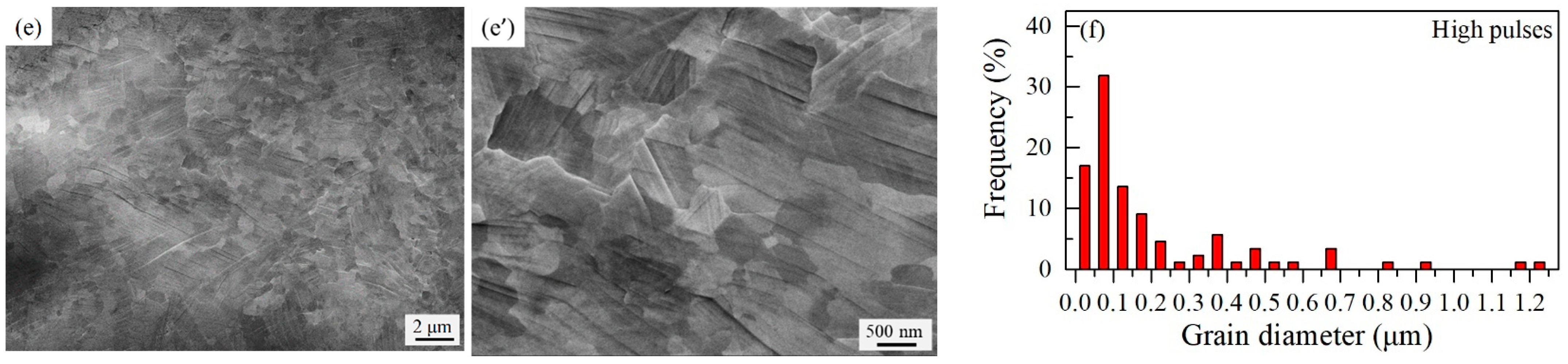
Figure 22 presents the grain diameter distribution in the main irradiation zone of the 304 stainless steel workpiece surface after different electron beam pulse irradiation. The proportions of sub-micron grains (<1 μm) and coarse grains (>10 μm) in the main irradiation zone after low, medium, and high pulse counts are compared to examine the degree of grain refinement with increasing pulse number. After low pulse count irradiation, the proportion of sub-micron grains (<1 μm) is 4.2%; after medium pulse counts, it increases to 23.1%; and after high pulse counts, it reaches 97.7%, representing an increase of 93.5 percentage points relative to the low pulse count condition. Regarding coarse grains (>10 μm), the proportion is 31.7% after low pulse counts, 23.1% after medium pulse counts, and nearly negligible after high pulse counts. It is evident that, under high pulse count electron beam irradiation, the degree of grain refinement is substantially greater than under low and medium pulse count conditions.
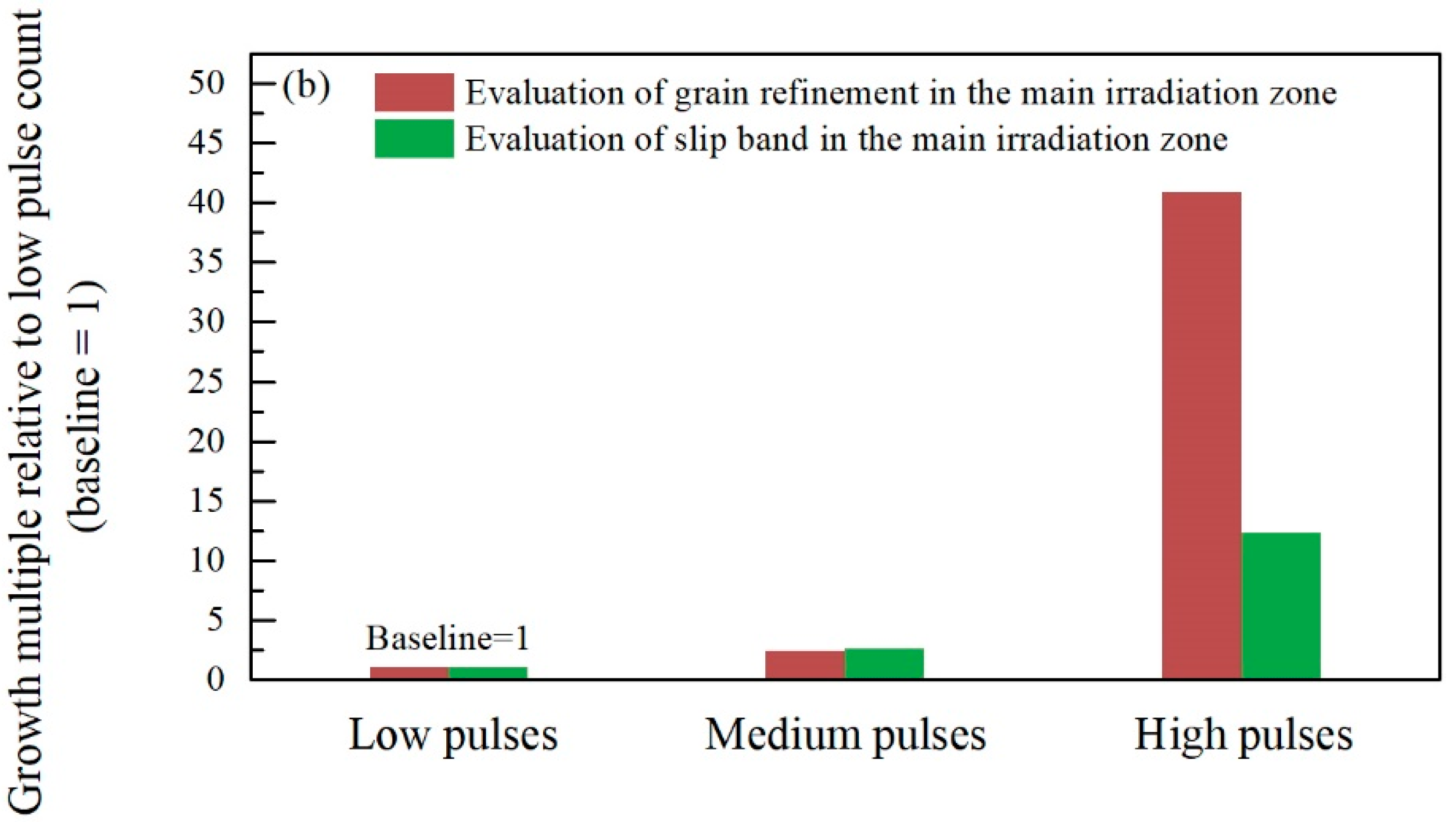
Based on the grain size distributions in the main irradiated zone after different pulse irradiation, the average grain diameter is calculated. Using the reciprocal of the grain diameter after low pulse count irradiation as the benchmark, the relative changes under medium and high pulse counts are expressed as multiples. The time integrals of the maximum temperature and maximum stress are again used as numerical measures of the thermal and stress conditions in the main irradiated zone. Growth multiples of grain refinement (reciprocal of average grain diameter), maximum temperature, and maximum stress under different pulse counts relative to low pulse count (baseline = 1) are shown in Figure 23a. For comparison with the degree of grain refinement, the variation in slip bands in the main irradiated zone under different pulses is quantitatively evaluated by calculating the total length of slip bands in all orientations, as shown in Figure 23b. From Figure 23a, it can be observed that, under high pulse counts, the increase in grain refinement, temperature, and stress far exceeds that under medium pulse counts. Specifically, the grain refinement index increases by a factor of 40, which is greater than the temperature increase (24×) and the stress increase (29×). From Figure 23b, it is seen that the increase in grain refinement under high pulse counts significantly surpasses the 11.3-fold increase in slip band length. These results indicate that both the rapid temperature variation and the high stress introduced by hollow cathode electron beam irradiation contribute to grain refinement, but the effect of rapid temperature variation is far more dominant than that of high stress in promoting plastic deformation. Since stress-induced grain refinement must first proceed through plastic deformation to form sub-grains, it can be concluded that, during hollow cathode electron beam surface irradiation, grain refinement is primarily driven by the rapid temperature distribution, which generates a large number of instantaneously solidified nucleation sites, while the formation of sub-grains through high stress-induced plastic deformation plays a secondary role.
The extremely high heating/cooling rates of the nanosecond pulsed electron beam (heating at 1011 K/s, cooling at 1010~109 K/s) are indeed much higher than those of traditional rapid solidification processes (102~106 K/s). This jump in magnitude brings about a fundamental change in the mechanism of grain refinement.
  • Explosive growth of nucleation rate driven by extreme supercooling
According to the classical nucleation theory (CNT), the nucleation rate of melt solidification is highly non-linearly related to the supercooling degree [47]. In traditional solidification processes (such as ingot casting and conventional quenching, with a cooling rate of 102~106 K/s), the supercooling degree is usually in the range of tens to hundreds of K, and the nucleation rate is limited, with grain sizes ranging from micrometers to millimeters. In nanosecond pulsed electron beams (extremely supercooling rate of 1010~109 K/s), the surface melt layer drops from approximately 2000 °C to the base temperature within tens of nanoseconds, generating a huge thermal supercooling degree (up to the order of 103 K). With each increase in a factor of ten in supercooling degree, the nucleation rate can increase exponentially by several orders of magnitude.
Under sub-rapid solidification conditions (102~103 K/s), the increase in supercooling degree can activate a large number of heterogeneous cores, reducing the grain size from millimeters to 73 μm [48]. While the cooling rate of the nanosecond pulsed electron beam is 7 to 8 orders of magnitude higher, its nucleation rate enhancement effect is more intense, enabling the formation of astronomically large crystal nuclei at the micrometer level, which is the fundamental reason for grain refinement to the sub-micrometer level (<1 μm accounting for 97.7%).
2.
Limited atomic migration and growth inhibition effect
The extreme cooling rate not only promotes nucleation but is also more important in inhibiting crystal growth. The crystal growth rate is controlled by atomic diffusion. The effect of the nanosecond pulsed electron beam is as follows:
Extreme compression of time scale: The melt layer exists for only tens of nanoseconds, and the atomic diffusion distance is limited to the nanoscale. At a cooling rate of 109~1010 K/s, crystal growth is limited by the atomic collision frequency, and solid-state phase transformation is completely suppressed [49].
Reversal of competitive mechanism: In traditional solidification, nucleation and growth occur simultaneously, and the grain is prone to grow. In the nanosecond pulsed condition, the nucleation process dominates, and the crystal nucleus is just formed before being “frozen”, without enough time to grow.
In the supercooled melt, the change in grain size is entirely determined by the nucleation rate at the beginning of solidification [47]. This is consistent with our observations—the proportion of sub-micrometer grains reaches 97.7% under high pulse frequency, indicating that almost all the formed grains are “frozen” at the initial size.
3.
Thermal stress-induced grain fragmentation effect
In addition to the melt solidification path, the extremely high heating rate of the nanosecond pulsed electron beam (1011 K/s) also contributes to grain refinement through the thermal stress mechanism:
Generation and propagation of thermal stress waves: Within tens of nanoseconds, the temperature changes by approximately 103 K, generating transient thermal stress of up to GPa level (Figure 12). When this stress wave propagates on the surface layer, it can cause dislocations, slip bands, and sub-grain boundaries to form within the grain.
Dynamic recovery and recrystallization: During the pulse interval, the combined effect of high temperature (not yet completely cooled) and stress can induce dynamic recovery and recrystallization, fragmenting coarse grains into fine sub-grains. In the “un-melted mode”, the strong current pulsed electron beam can achieve surface grain refinement and texture transformation through repeated deformation and recovery recrystallization.
It is worth noting that our quantitative analysis shows (Figure 23) that the growth of grain refinement (40 times) is much greater than the growth of slip bands (11.3 times), indicating that the contribution of the thermal-induced nucleation mechanism to grain refinement is much greater than that of the stress-induced fragmentation mechanism, and the primary and secondary relationships are clear.

4. Conclusions

Based on a temperature–stress coupling simulation approach, a heat source model was proposed for surface modification using a nanosecond pulsed hollow cathode electron beam. This study investigated the dynamic thermal-stress changes induced by electron beam interaction with material surfaces and the influence of thermal stress on surface micro–nano characteristics. Systematic analyses were conducted on the dynamic temperature/stress distribution results in the micron-scale surface layer of the workpiece after nanosecond pulsed hollow cathode electron beam irradiation, encompassing aspects such as the dynamic variations in maximum temperature/stress in the surface micron layer, temperature/stress changes in the cross-sectional remelted layer, and variations in surface heating/cooling rates. Furthermore, the rationality of the aforementioned heat source model for surface modification using nanosecond pulsed hollow cathode electron beams was validated. Subsequently, in conjunction with hollow cathode electron beam irradiation experiments under low, medium, and high pulse counts, the effects of thermal and stress conditions on the evolution of surface micromorphology and grain refinement in the irradiated workpiece were investigated. Through quantitative correlation analyses, the underlying mechanisms of morphological evolution and grain refinement were further elucidated. The conclusions drawn are as follows:
  • The irradiation effects of the nanosecond pulsed hollow cathode electron beam on the workpiece surface are highly localized, confined to a small region of approximately 1.5–2 mm, while other areas of the substrate remain essentially unaffected. Within this interaction zone, extreme thermal and stress variations occur: temperature changes on the order of ~103 K and stress variations ranging from 103 to 104 MPa within tens of nanoseconds. Moreover, a heat accumulation effect is observed, which intensifies with increasing pulse count. The heating rates of the nanosecond pulsed hollow cathode electron beam consistently reach the order of 1011 K/s, while cooling rates range from 109 to 1010 K/s, exceeding those of microsecond pulsed electron beams by one to two orders of magnitude.
  • Nanosecond pulsed electron beam irradiation experiments demonstrate that under low, medium, and high pulse counts, the simulated remelted zone diameters and remelted layer thicknesses are in good agreement with experimental results. This confirms the validity of the established heat source model for surface modification using nanosecond pulsed hollow cathode electron beams.
  • The rise time of the hollow cathode nanosecond pulsed electron beam is approximately 10 ns, with a pulse duration of about 100 ns. During this process, temperatures reach several thousand kelvin, and stress levels reach several gigapascals. Consequently, the rates of temperature and stress change in the primary irradiation zone are extremely high, placing the surface in a highly non-equilibrium state. Under the influence of such temperature and stress conditions, the workpiece surface undergoes flow and compressive deformation, generating significant topographic height differences. This compressive effect intensifies with increasing pulse count and outweighs the filling effect of additional pulses on crater morphology. Finally, based on the numerical correlation between thermal/stress conditions and the degree of grain refinement under different pulse counts, it is further concluded that, during nanosecond hollow cathode electron beam surface irradiation, grain refinement is predominantly governed by the rapid temperature distribution, which generates a large number of instantaneously solidified nucleation sites, while the formation of sub-grains through high-stress-induced plastic deformation plays a secondary role.

Author Contributions

Conceptualization, Y.H. and Z.H.; methodology, Y.H.; software, Y.H.; validation, Y.H., X.C. and Z.H.; formal analysis, X.C. and Z.H.; investigation, Y.H.; resources, Y.H. and X.C.; data curation, X.C.; writing—original draft preparation, Y.H.; writing—review and editing, Z.H.; visualization, Z.H.; supervision, X.C.; project administration, Z.H.; funding acquisition, Y.H. and Z.H. All authors have read and agreed to the published version of the manuscript.

Funding

This research was funded by the College-level Key Project of Xuzhou College of Industrial Technology, grant number XGY2024ZXWT05.

Institutional Review Board Statement

Not applicable.

Informed Consent Statement

Not applicable.

Data Availability Statement

The data that support the findings of this study are available from the corresponding author upon reasonable request.

Conflicts of Interest

Author Xiaotong Cao was employed by the company Jiangsu XCMG Construction Machinery Research Institute Co., Ltd. The remaining authors declare that the research was conducted in the absence of any commercial or financial relationships that could be construed as a potential conflict of interest.

References

  1. Cao, X.; Hu, J.; Huo, W.; Xi, X.; Zhao, W. Surface microstructure and property modifications in AISI 304 stainless steel induced by pseudospark pulsed electron beam treatments. Vacuum 2021, 184, 109914. [Google Scholar] [CrossRef]
  2. Favre, M.; Choi, P.; Chuaqui, H.; Mitchell, I.; Wyndham, E.; Leñero, A.M. Experimental investigation of ionization growth in the pre-breakdown phase of fast pulsed capillary discharges. Plasma Sources Sci. Technol. 2003, 12, 78–84. [Google Scholar] [CrossRef]
  3. Frank, K.; Stark, R.; Christiansen, J.; Felsner, P.; Gortler, A.; Hoffmann, D.; Prucker, U.; Schwandner, A.; Stetter, M.; Tkotz, R.; et al. Spatial and time characteristics of high current, high voltage pseudospark discharges. IEEE Trans. Plasma Sci. 1997, 25, 740–747. [Google Scholar] [CrossRef]
  4. Wang, H.; Long, F.; Liang, Z.; Cai, S.; Lv, R.; Hao, S. Surface Evolution and Performance of 45CrNiMoV Steel Modified by Electron Beam Irradiation. Coatings 2025, 15, 1335. [Google Scholar] [CrossRef]
  5. Frank, K.; Christiansen, J. The fundamentals of the pseudospark and its applications. IEEE Trans. Plasma Sci. 1989, 17, 748–753. [Google Scholar] [CrossRef]
  6. Christiansen, J.; Lieser, N.; Rath, W.; Steudtner, W.; Rózsa, K.; Jánossy, M.; Apai, P.; Mezei, P. Pulsed laser oscillation at 488.0 nm and 514.5 nm in an Ar-He Pseudospark discharge. Opt. Commun. 1985, 56, 39–40. [Google Scholar] [CrossRef]
  7. Valkov, S.; Kotlarski, G.; Parshorov, S.; Ormanova, M.; Padikova, F.; Stoyanov, B.; Parshorov, I. Electron Beam Surface Treatment and Its Impact on the Plasticity of Fe-Based High-Entropy Alloy. Coatings 2025, 15, 477. [Google Scholar] [CrossRef]
  8. Jiang, C.; Kuthi, A.; Gundersen, M.A. Toward ultracompact pseudospark switches. Appl. Phys. Lett. 2005, 86, 24105. [Google Scholar] [CrossRef]
  9. Kozyrev, A.V.; Korolev, Y.D.; Rabotkin, V.G.; Shemyakin, I.A. Processes in the prebreakdown stage of a low-pressure discharge and the mechanism of discharge initiation in pseudospark switches. J. Appl. Phys. 1993, 74, 5366–5371. [Google Scholar] [CrossRef]
  10. Rosier, O.; Apetz, R.; Bergmann, K.; Jonkers, J.; Wester, R.; Neff, W.; Pankert, J. Frequency scaling in a hollow-cathode-triggered pinch plasma as radiation source in the extreme ultraviolet. IEEE Trans. Plasma Sci. 2004, 32, 240–246. [Google Scholar] [CrossRef]
  11. Boeuf, J.P.; Pitchford, L.C. Pseudospark discharges via computer simulation. IEEE Trans. Plasma Sci. 1991, 19, 286–296. [Google Scholar] [CrossRef]
  12. Boggasch, E.; Rhee, M.J. High-brightness pseudospark-produced electron beam. Appl. Phys. Lett. 1990, 56, 1746–1748. [Google Scholar] [CrossRef]
  13. Dewald, E.; Frank, K.; Hoffmann, D.; Stark, R.; Ganciu, M.; Mandache, B.; Nistor, M.; Pointu, A.-M.; Popescu, I.-I. Pulsed intense electron beams generated in transient hollow cathode discharges: Fundamentals and applications. IEEE Trans. Plasma Sci. 1997, 25, 272–278. [Google Scholar] [CrossRef]
  14. Cetiner, S.O.; Stoltz, P.; Messmer, P.; Cambier, J.-L. Dependence of electron peak current on hollow cathode dimensions and seed electron energy in a pseudospark discharge. J. Appl. Phys. 2008, 103, 23304. [Google Scholar] [CrossRef]
  15. Tkotz, R.; Gortler, A.; Christiansen, J.; Dollinger, S.; Frank, K.; Heine, F.; Herleb, U.; Insam, S.; Kowalewicz, R.; Mehr, T.; et al. Pseudospark switches-technological aspects and application. IEEE Trans. Plasma Sci. 1995, 23, 309–317. [Google Scholar] [CrossRef]
  16. Dewald, E.; Frank, K.; Hoffmann, D.H.H.; Tauschwitz, A. Comparative studies on intense electron beams generated in transient hollow-cathode discharges. IEEE Trans. Plasma Sci. 2002, 30, 1820–1826. [Google Scholar] [CrossRef]
  17. Krasik, Y.E.; Gleizer, S.; Chirko, K.; Gleizer, J.Z.; Felsteiner, J.; Bernshtam, V.; Matacotta, F.C. Characterization of a channel spark discharge and the generated electron beam. J. Appl. Phys. 2006, 99, 63303. [Google Scholar] [CrossRef]
  18. Kumar, N.; Narayan Pal, U.; Kumar Pal, D.; Prajesh, R.; Prakash, R. Experimental investigation of a 1 kA/cm2 sheet beam plasma cathode electron gun. Rev. Sci. Instrum. 2015, 86, 13503. [Google Scholar] [CrossRef] [PubMed]
  19. Jain, K.K.; Boggasch, E.; Reiser, M.; Rhee, M.J. Experimental investigation of a pseudospark-produced high-brightness electron beam. Phys. Fluids B Plasma Phys. 1990, 2, 2487–2491. [Google Scholar] [CrossRef]
  20. Petrov, P.; Dechev, D.; Ivanov, N.; Hikov, T.; Valkov, S.; Nikolova, M.; Yankov, E.; Parshorov, S.; Bezdushnyi, R.; Andreeva, A. Study of the influence of electron beam treatment of Ti5Al4V substrate on the mechanical properties and surface topography of multilayer TiN/TiO2 coatings. Vacuum 2018, 154, 264–271. [Google Scholar] [CrossRef]
  21. Qin, Y.; Zou, J.; Dong, C.; Wang, X.; Wu, A.; Liu, Y.; Hao, S.; Guan, Q. Temperature–stress fields and related phenomena induced by a high current pulsed electron beam. Nucl. Instrum. Methods Phys. Res. Sect. B Beam Interact. Mater. At. 2004, 225, 544–554. [Google Scholar] [CrossRef]
  22. Zhang, L.; Peng, C.-T.; Yao, X.; Guan, Q.; Lu, R. Surface alloying of Cr on Ti6Al4V alloy induced by high-current pulse electron beam. Surf. Coat. Technol. 2019, 370, 288–297. [Google Scholar] [CrossRef]
  23. Duan, C.; Wu, T.; Zou, J.; Zhang, K. Surface modifications of a Mg-10Li-5Zn-0.5Er magnesium alloy by high-current pulsed electron beam. J. Mater. Res. Technol. 2026, 41, 3228–3241. [Google Scholar] [CrossRef]
  24. Gao, B.; Hao, S.; Zou, J.; Wu, W.; Tu, G.; Dong, C. Effect of high current pulsed electron beam treatment on surface microstructure and wear and corrosion resistance of an AZ91HP magnesium alloy. Surf. Coat. Technol. 2007, 201, 6297–6303. [Google Scholar] [CrossRef]
  25. Hao, S.; Wu, P.; Zou, J.; Grosdidier, T.; Dong, C. Microstructure evolution occurring in the modified surface of 316L stainless steel under high current pulsed electron beam treatment. Appl. Surf. Sci. 2007, 253, 5349–5354. [Google Scholar] [CrossRef]
  26. Hao, S.Z.; Wu, P.S.; Grosdidier, T.; Dong, C. Surface Microstructure and Corrosion Resistance of 316L Stainless Steel after High Current Pulsed Electron Beam Treatment. Mater. Sci. Forum 2007, 561–565, 2381–2384. [Google Scholar] [CrossRef]
  27. Zhang, K.; Zou, J.; Grosdidier, T.; Gey, N.; Yang, D.; Hao, S.; Dong, C. Surface modification of Ni (50.6at.%) Ti by high current pulsed electron beam treatment. J. Alloys Compd. 2007, 434–435, 682–685. [Google Scholar] [CrossRef]
  28. Hao, S.; Zhang, X.; Mei, X.; Grosdidier, T.; Dong, C. Surface treatment of DZ4 directionally solidified nickel-based superalloy by high current pulsed electron beam. Mater. Lett. 2008, 62, 414–417. [Google Scholar] [CrossRef]
  29. Kang, E.G.; Choi, H.; Min, B.-K.; Lee, S.J. Austenite phase transformation of SKD11 by surface heat treatment with a focused electron beam. Surf. Coat. Technol. 2017, 321, 247–256. [Google Scholar] [CrossRef]
  30. Wang, H.; Li, L.; Qiu, S.; Zhai, W.; Li, Q.; Hao, S. Evolution of Microstructure at the Surface of 40CrNiMo7 Steel Treated by High-Current Pulsed Electron Beam. Coatings 2020, 10, 311. [Google Scholar] [CrossRef]
  31. Zhang, C.; Cai, J.; Lv, P.; Zhang, Y.; Xia, H.; Guan, Q. Surface microstructure and properties of Cu-C powder metallurgical alloy induced by high-current pulsed electron beam. J. Alloys Compd. 2017, 697, 96–103. [Google Scholar] [CrossRef]
  32. Cai, J.; Guan, Q.; Lv, P.; Zhang, C.; Yin, Y. Crater Formation on the Surface of Pure Metal and Alloy Irradiated by High Current Pulsed Electron Beam. High Temp. Mater. Process. 2018, 37, 777–784. [Google Scholar] [CrossRef]
  33. Kravets, V.A.; Dementeva, E.V.; Bakaleinikov, L.A.; Zamoryanskaya, M. Electron beam surface heating: A model incorporating effective atomic number with experimental validation. Mater. Chem. Phys. 2026, 349, 131764. [Google Scholar] [CrossRef]
  34. Qin, Q.; Wang, R.; Wei, D.; Li, X.; Lu, J. An analytical model and experimental validation of annular heat source during scanning electron beam treatment. Int. J. Therm. Sci. 2024, 196, 108742. [Google Scholar] [CrossRef]
  35. Joshi, S.; Hildebrand, J.; Aloraier, A.S.; Rabczuk, T. Characterization of material properties and heat source parameters in welding simulation of two overlapping beads on a substrate plate. Comput. Mater. Sci. 2013, 69, 559–565. [Google Scholar] [CrossRef]
  36. Vine, J.; Einstein, P.A. Heating effect of an electron beam impinging on a solid surface, allowing for penetration. Proc. Inst. Electr. Eng. 1964, 111, 921–930. [Google Scholar] [CrossRef]
  37. Henry, H.; Stavros, A.A. Mathematical modelling of solidification and melting: A review. Model. Simul. Mater. Sci. Eng. 1996, 4, 371. [Google Scholar] [CrossRef]
  38. Hu, J.; Fu, Y.; Li, D.; Zhu, Y.; Zhang, R.; Zhao, W. Hybrid particle-thermodynamic model and experimental validation of multi-track periodical heating during electron beam treatment. Nucl. Instrum. Methods Phys. Res. Sect. B Beam Interact. Mater. At. 2019, 439, 34–42. [Google Scholar] [CrossRef]
  39. Pakowski, Z. Fundamentals of Heat and Mass Transfer, Frank P Incropera, David P DeWitt, Theodore L Bergman, Adrienne S Lavine, J. Wiley & Sons, Hoboken NJ (2007), 997 pp. Chem. Eng. Res. Des. 2007, 85, 1683–1684. [Google Scholar] [CrossRef]
  40. Gilbey, D.M. Theory of Thermal Stresses. J. Less Common Met. 1959, 1, 139–144. [Google Scholar] [CrossRef]
  41. Bogaard, R.H.; Desai, P.D.; Li, H.H.; Ho, C.Y. Thermophysical properties of stainless steels. Thermochim. Acta 1993, 218, 373–393. [Google Scholar] [CrossRef]
  42. Bowling, T.S. Thermal Radiation Heat Transfer: Siegel, R. and Howell, J.R., 3rd edition, 1992. Hemisphere (Taylor and Francis), £50.00 sb, ISBN 0-89116-271-2. J. Atmos. Terr. Phys. 1994, 56, 539–540. [Google Scholar] [CrossRef]
  43. Huo, W.; He, W.; Han, L.; Zhu, K.; Wang, F. Study of nanosecond pulsed hollow-cathode electron beam generation and transportation based on PIC-MCC simulation. Mater. Today Commun. 2024, 38, 108108. [Google Scholar] [CrossRef]
  44. Ghosh, A.; Chattopadhyaya, S. Analytical solution for transient temperature distribution of semi -infinite body subjected to 3-D moving heat source of submerged Arc Welding process. In Proceedings of the 2010 International Conference on Mechanical and Electrical Technology, Singapore, 10–12 September 2010; Institute of Electrical and Electronics Engineers (IEEE): New York, NY, USA, 2010; pp. 733–737. [Google Scholar] [CrossRef]
  45. Fujita, H.; Taguchi, E. Penetration of Electrons in Materials. Jpn. J. Appl. Phys. 1982, 21, L414. [Google Scholar] [CrossRef]
  46. Liu, Y.R.; Zhang, K.M.; Zou, J.X.; Liu, D.K.; Zhang, T.C. Effect of the high current pulsed electron beam treatment on the surface microstructure and corrosion resistance of a Mg-4Sm alloy. J. Alloys Compd. 2018, 741, 65–75. [Google Scholar] [CrossRef]
  47. Wang, P.; Liu, F.; Lu, Y.P.; Yang, C.L.; Yang, G.C.; Zhou, Y.H. Grain refinement and coarsening in hypercooled solidification of eutectic alloy. J. Cryst. Growth 2008, 310, 4309–4313. [Google Scholar] [CrossRef]
  48. Nowak, M.; Bolzoni, L.; Hari Babu, N. Grain refinement of Al–Si alloys by Nb–B inoculation. Part I: Concept development and effect on binary alloys. Mater. Des. (1980–2015) 2015, 66, 366–375. [Google Scholar] [CrossRef]
  49. Vitta, S. Rapid solidification of polymorphic transition metals induced by nanosecond laser pulses. Appl. Phys. Lett. 1991, 59, 411–413. [Google Scholar] [CrossRef]
Figure 1. Interpolation of thermal conductivity (a) and constant-pressure heat capacity (b).
Coatings 16 00352 g001
Figure 2. Interpolation of density.
Coatings 16 00352 g002
Figure 3. Geometric diagrams of the two boundary conditions: (a) diffuse reflection; (b) thermal insulation.
Coatings 16 00352 g003
Figure 4. The mesh generation in the solving domain.
Coatings 16 00352 g004
Figure 5. Gaussian heat flux distribution of electron beam.
Coatings 16 00352 g005
Figure 6. Voltage, current, and power of electron beam pulse vary with time under experimental measurement. (a) voltage waveform of one pulse; (b) voltage waveform of fivecanse.ativellulsesl; (c) current waveform of one pulse; (d) current waveform of five consecutive pulses; (e) power waveform of one consecutive pulse; (f) power waveform of five consecutive pulses.
Coatings 16 00352 g006aCoatings 16 00352 g006b
Figure 7. Electron beam pulse power varies with time of simulation input.
Coatings 16 00352 g007
Figure 8. The variation in the energy deposition coefficient within the range of incident electrons with depth.
Coatings 16 00352 g008
Figure 9. The 3D temperature distribution contour on the 304 stainless steel workpiece at t = 2000 ns (end of 10th pulse), showing the localized heating effect of nanosecond pulsed hollow cathode electron beam.
Coatings 16 00352 g009
Figure 10. The 3D stress distribution contour on the 304 stainless steel workpiece at t = 2000 ns (end of 10th pulse), showing the correspondence between high temperature zone and high stress zone.
Coatings 16 00352 g010
Figure 11. The variation in the maximum temperature in the 304 stainless steel working area with time.
Coatings 16 00352 g011
Figure 12. The variation in the maximum stress in the 304 stainless steel working area with time.
Coatings 16 00352 g012
Figure 13. The 2D temperature distribution contour under different pulses at different time steps on the 304 stainless steel workpiece (above the melting point), (ad) at the end of the pulse processing and before the start of the next pulse (including the time interval between two pulses), (e,f) just after the end of the pulse irradiation heating (excluding the interval time): (a) three pulses at 600 ns; (b) five pulses at 1000 ns; (c) seven pulses at 1400 ns; (d) nine pulses at 1800 ns; (e) three pulses at 420 ns; (f) seven pulses at 1220 ns.
Coatings 16 00352 g013
Figure 14. The 2D stress distribution contour under different pulses at different time steps on the 304 stainless steel workpiece, (a,b) at the end of the pulse processing and before the start of the next pulse (including the time interval between two pulses), (c,d) just after the end of the pulse irradiation heating (excluding the interval time): (a) three pulses; (b) seven pulses; (c) three pulses at 420 ns; (d) seven pulses at 1220 ns.
Coatings 16 00352 g014aCoatings 16 00352 g014b
Figure 15. The variation in the rates of heating (a) and cooling (b) in the 304 stainless steel working area with the pulse number.
Coatings 16 00352 g015
Figure 16. Physical diagram of the experimental device for measuring the waveform of hollow cathode electron beam current: 1—discharge chamber, 2—vacuum chamber, 3—high voltage pulse network, 4—the system of vacuum pump, 5—the support of vacuum chamber, 6—water cooling device, 7—power supply and measurement control system.
Coatings 16 00352 g016
Figure 17. Experimental setup for measuring the hollow cathode electron beam current waveform.
Coatings 16 00352 g017
Figure 18. Comparisons between simulation results and experimental results of the thickness and diameter of the remelting layer under high pulse number: (a,c) are the experimental results; (b,d) are the simulation results.
Coatings 16 00352 g018
Figure 19. Comparisons between simulation results and experimental results of the diameter (a) and thickness (b) of the remelting zone.
Coatings 16 00352 g019
Figure 20. Height difference in the micromorphology at the main irradiation zone of 304 stainless steel surface under different electron beam pulse numbers: (a,b) low pulses; (c,d) medium pulses; (e,f) high pulses.
Coatings 16 00352 g020aCoatings 16 00352 g020b
Figure 21. Growth multiples of surface morphological profile, maximum temperature, and maximum stress under different pulse counts relative to low pulse count (baseline = 1). The morphological profile is quantified by the product of irradiation zone diameter and average height difference (D × Δh). Temperature and stress are evaluated by time integration of maximum values over the irradiation zone.
Coatings 16 00352 g021
Figure 22. Distribution of grain diameter on 304 stainless steel workpiece surface after different electron beam pulses irradiation: (a,a’,b) low pulses; (c,c’,d) medium pulses; (e,e’,f) high pulses.
Coatings 16 00352 g022aCoatings 16 00352 g022b
Figure 23. (a) Growth multiples of grain refinement (reciprocal of average grain diameter), maximum temperature, and maximum stress under different pulse counts relative to low pulse count (baseline = 1). (b) Comparison of growth multiples between grain refinement and plastic deformation (total length of slip bands) under different pulse counts relative to low pulse count.
Coatings 16 00352 g023aCoatings 16 00352 g023b
Table 1. Electron beam simulation parameters with pulse number as variable.
NameValue
Discharge voltage22 kV
Beam current200 A
Pulse duration20 ns
Pulse interval time180 ns
Pulse number1–10
Beam spot diameter3 mm
Table 2. The absolute error and relative percentage error of the remelted zone diameter.
Pulse NumberExperimental Diameter/μmSimulated Diameter/μmAbsolute Error/μmRelative Error/%
Low pulse9094+44.4%
Medium pulse180171−95.0%
High pulse300288−124.0%
Table 3. The absolute error and relative percentage error of the remelted layer thickness.
Pulse NumberExperimental Thickness/μmSimulated Thickness/μmAbsolute Error/μmRelative Error/%
Low pulse1.51.6+0.16.7%
Medium pulse2.83.0+0.27.1%
High pulse4.54.500%
Disclaimer/Publisher’s Note: The statements, opinions and data contained in all publications are solely those of the individual author(s) and contributor(s) and not of MDPI and/or the editor(s). MDPI and/or the editor(s) disclaim responsibility for any injury to people or property resulting from any ideas, methods, instructions or products referred to in the content.