
Article

Density Functional Theory Study of Electronic Structure and Optical Properties of W-Doped γ-Bi2MoO6

1
Shaanxi Key Laboratory of Intelligent Processing for Big Energy Data, School of Physics and Electronic Information, Yan’an University, Yan’an 716000, China
2
School of Physical Science and Technology, Inner Mongolia University, Hohhot 010021, China
*
Authors to whom correspondence should be addressed.
Coatings 2026, 16(3), 338; https://doi.org/10.3390/coatings16030338

Submission received: 13 February 2026 / Revised: 6 March 2026 / Accepted: 6 March 2026 / Published: 9 March 2026

Abstract

We employed density functional theory (DFT) to investigate the effect of tungsten (W) doping on the crystal structure, electronic properties, and optical response of Bi2MoO6−xWxO6. The results show that W doping retains the Aurivillius orthorhombic lattice structure while inducing localized distortions. All doping systems retain semiconductor characteristics with a band gap ranging from 2.11 to 2.26 eV. The valence band is mainly composed of O-2p orbitals, while the conduction band consists of Mo-4d and W-5d states. As W doping increases, the influence of W-5d states near the conduction band edge intensifies, modulating the electronic structure. Optical calculations show that W doping shifts the absorption edge and allows for precise adjustment of the absorption threshold in the visible light range. These findings provide insight into how W doping affects the electronic and optical properties of γ-Bi2MoO6 and offer a theoretical basis for improving Bi2MoO6-based photocatalytic materials.

1. Introduction

As industrialization progresses, it brings serious issues, such as the rapid depletion of fossil fuels and the worsening of pollution. Currently, the world faces two major crises—energy shortages and environmental degradation—that strain our ability to sustain development [1,2]. As we demand more energy, CO2 emissions are skyrocketing, which only makes climate change and the greenhouse effect worse [3]. At the same time, we are dumping industrial and household wastewater into the environment in huge amounts, and that is causing organic pollutants to pile up in our water systems, putting ecosystems at serious risk [4]. Considering these challenges, finding green, efficient, and affordable photocatalytic materials capable of converting solar energy into clean fuel has become a key solution for addressing both energy and environmental crises [5,6]. Photocatalysis, which harnesses sunlight, produces no secondary pollution, and relies on simple processes, is increasingly attracting attention [7]. Visible-light-based photocatalysts, with their high light absorption efficiency over a broad wavelength range and low excitation energy requirements, are seen as pivotal to future photocatalysis technologies, garnering extensive scholarly attention [8].
γ-Bi2MoO6, a typical Aurivillius-type oxide, has a layered structure composed of alternating (Bi2O2)2+ layers and (MoO4)2− layers, which plays a crucial role in enhancing photocatalytic performance [9]. This structure improves photocatalytic efficiency through two main mechanisms. First, it facilitates the separation of photoelectrons and holes and reduces recombination [10]. Second, it promotes the formation of more active sites on the surface, which enhances the adsorption and activation of reactant molecules, thus improving catalytic activity [11]. The band gap of γ-Bi2MoO6, ranging from 2.5 to 2.8 eV, allows for efficient visible light absorption and provides strong redox ability suitable to degrade organic pollutants and to decompose water [12,13]. Despite some limitations, the material shows potential for further improving light absorption and carrier dynamics. However, its narrow band gap limits the light absorption range, and lower intrinsic electron mobility may hinder photocatalytic efficiency. Doping with rare-earth or transition metals increases active sites and introduces intermediate energy levels, thus broadening the light absorption range and enhancing photocarrier migration [14,15,16]. γ-Bi2MoO6 also demonstrates good chemical stability, maintaining its activity and structural integrity even after prolonged use, making it a strong candidate for real-world applications such as pollutant degradation, nitrogen fixation, and water splitting for hydrogen production [17,18]. This stability is essential for continuous processes and long-term tasks.
Tungsten (W) doping enhances γ-Bi2MoO6 by lowering its band gap by 0.4 eV, from 2.7 eV to 2.3 eV [19]. This shift results from W replacing some Mo atoms in the lattice, which causes lattice distortions that modify the material’s electronic structure and optical properties. The reduction in the band gap improves visible light absorption, which leads to higher photocatalytic efficiency. Experiments show that tungsten doping increases ammonia production by more than five times and improves the degradation of organic pollutants [20,21,22]. Cao et al. reported that W doping in MoO3 significantly improved the photo-induced charge transfer, enhancing surface-enhanced Raman spectroscopy (SERS) performance for environmental monitoring [23]. Future research should focus on optimizing the balance between stability and activity by investigating how tungsten concentration affects the material’s properties and the kinetics of interface charge transfer. Similarly, Sha et al. used DFT calculations to study W doping in diamond and found that carbon vacancies significantly reduced the formation energy of tungsten doping, promoting its incorporation into the diamond structure [24]. Both density functional theory (DFT) calculations and experimental results confirm that tungsten-doped γ-Bi2MoO6 is a versatile photocatalytic platform for applications such as pollutant degradation, nitrogen fixation, and water decomposition. In addition, in research by Cao et al., W doping in ZnS effectively enhanced photocatalytic CO2 reduction performance by improving carrier extraction and transfer efficiency through the creation of Zn and S vacancies [25]. Understanding the relationship between doping concentration and performance will guide the development of targeted design strategies.

2. Theoretical Model and Computational Methods

2.1. Theoretical Model

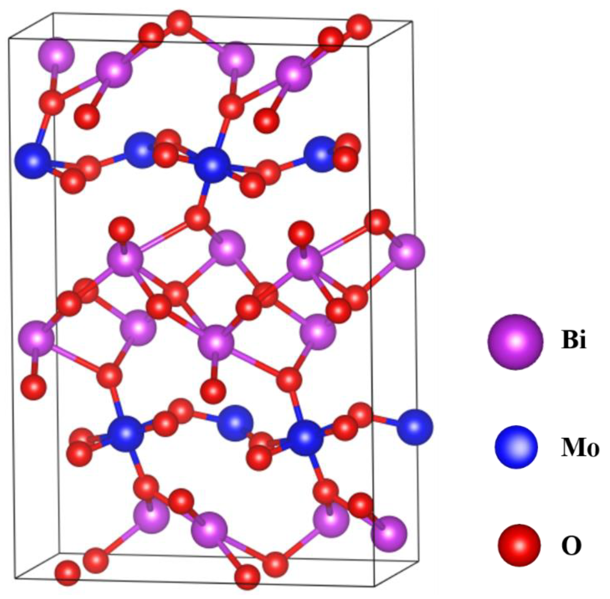
γ-Bi2MoO6 forms an orthorhombic crystal structure (space group Pca21), with unit cell dimensions of a = 5.527 Å, b = 5.528 Å, c = 16.298 Å, and all angles (α, β, γ) set to 90°. The volume of the unit cell amounts to 497.97 Å3. Inside the cell, the atomic layout includes two distinct Bi3+ sites, one Mo6+ site, and six different O2− ions. There are six positions for Bi3+ and seven for Mo6+, with four distinct O2− positions [9]. Our model construction is based on the number of Bi atoms, and γ-Bi2MoO6 adopts 2 × 1 × 1 supercrystalline cells as the calculation model. The structural model is shown in Figure 1.

2.2. Computational Method

All simulations were performed using the DS-PAW code [26,27] with a plane-wave basis set framework. Electron–ion interactions and exchange–correlation effects were described using the projector-augmented wave (PAW) method and the Perdew–Burke–Ernzerhof (PBE) functional under the generalized gradient approximation (GGA), respectively [28]. A plane-wave kinetic energy cutoff of 350 eV was employed. To ensure the accuracy of the results, convergence tests were performed for both the cutoff energy and k-point mesh (Figures S1 and S2). The total energy converged at a cutoff energy of 350 eV, with no significant changes observed when the cutoff was further increased. The k-point mesh was tested for convergence, and a 4 × 2 × 6 Monkhorst–Pack grid was found to be sufficient, with total energy differences between consecutive meshes becoming negligible. Geometry optimizations were considered converged when energy changes between steps fell below 1.0 × 10⁻⁵ eV/atom, atomic forces were smaller than 0.01 eV/Å, and the maximum stress was under 0.02 GPa. The Brillouin zone was sampled using a 4 × 2 × 6 Monkhorst–Pack k-point mesh. Band structures were plotted along the high-symmetry path G (0,0,0) → Z (0,0,0.5) → T (−0.5,0,0.5) → Y (−0.5,0,0) → S (−0.5,0.5,0) → X (0,0.5,0) → U (0,0.5,0.5) → R (−0.5,0.5,0.5). The valence electron configurations were Bi (6s26p35d10), O (2s22p4), Mo (4s25s14p64d5), and W (5s26s25p65d4). For optical calculations, a broadening parameter of 0.02 eV was used to simulate the effects of intrinsic broadening in the material. No intraband Drude contributions were included in the calculations.

3. Results and Discussion

3.1. Geometric Structure

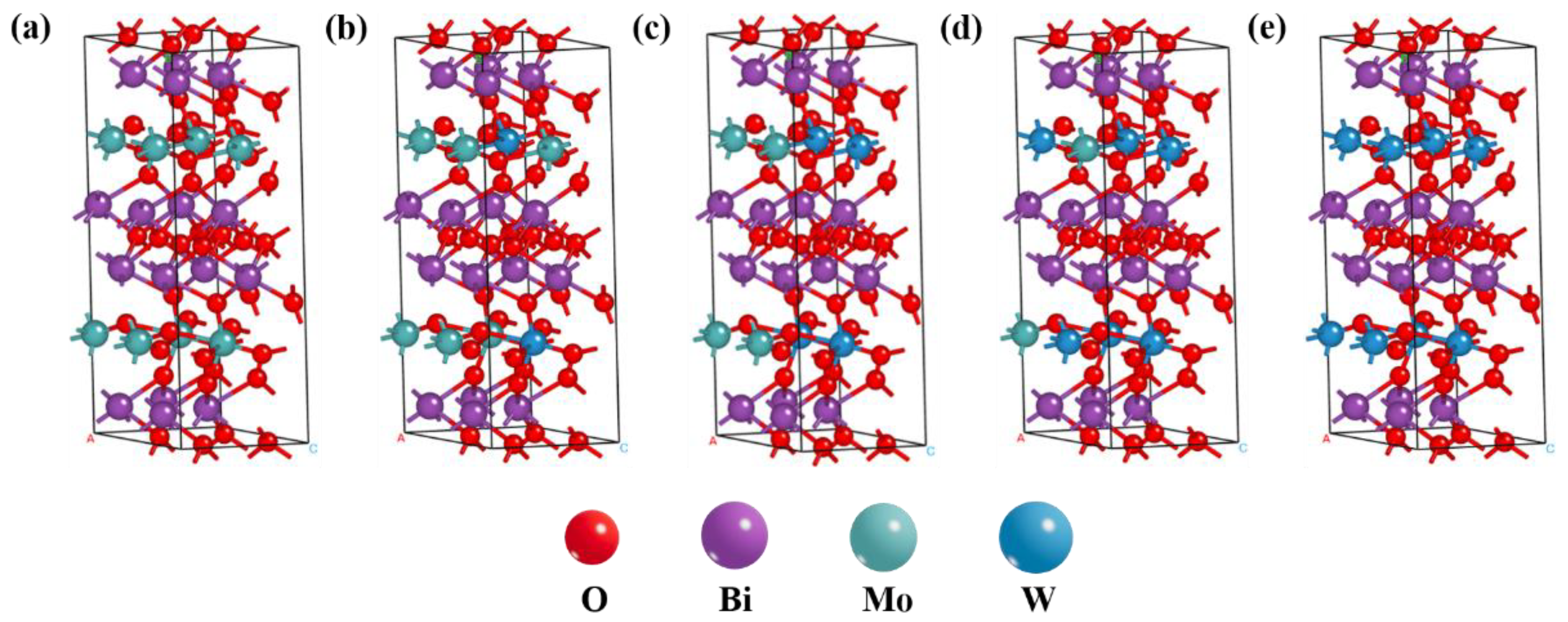
We used DFT calculations to optimize the geometric structures of γ-Bi2MoO6 and Bi2Mo1−xWxO6 with tungsten doping concentrations of x = 0.25, 0.50, and 0.75. Figure 2 shows the doping model in a 2 × 1 × 1 supercell, where tungsten atoms replace molybdenum. The labels 0W, 2W, 4W, 6W, and 8W correspond to the number of tungsten atoms substituted for molybdenum, representing doping levels of x = 0, 0.25, 0.50, 0.75, and 1. As shown in Table 1, the optimized lattice parameters a, b, and c match well with experimental data, with an average error of about 2%. To study the properties of electrons and interfaces, we built a 2 × 1 × 1 supercell model with a long axis (b) of about 16 Å. Compared to the experimental value, the length is slightly higher, which is consistent with the results in reference [29] regarding the behavior of the PBE functional and potential temperature effects. W doping causes an anisotropic lattice response, mainly along the b-axis direction (Table 1). This leads to selective expansion of the b-axis (16.583 → 16.76 Å), while the other directions remain unchanged (Figure 2), making it the primary lattice relaxation channel. Regarding bond lengths (Table S1), the M-O bond length (Mo-O) gradually increases with increasing W concentration, with the Mo-O bond length increasing from 1.78247 Å at 0W to 1.81282 Å at 8W, indicating the influence of W doping on the Mo-O bond. Similarly, the W-O bond length increases from 1.79530 Å at 2W to 1.81282 Å at 8W, reflecting the larger atomic radius of W compared to Mo. Lattice relaxation occurs primarily in this direction. Doping does not cause uniform expansion but induces local distortion by altering the Mo/W–O bond and interlayer stacking method, leaving the orthogonal main framework mostly intact [30]. Regarding the oxygen stoichiometry, it is important to note that tungsten (W) replaces molybdenum (Mo) without altering the overall oxygen content. Since both W and Mo have the same oxidation state (+6), the number of oxygen atoms remains unchanged during doping. Therefore, the oxygen stoichiometry in the material is preserved, ensuring charge balance while allowing for the substitution of Mo with W in the crystal structure.

3.2. Electronic Structure Information

3.2.1. Band Structure

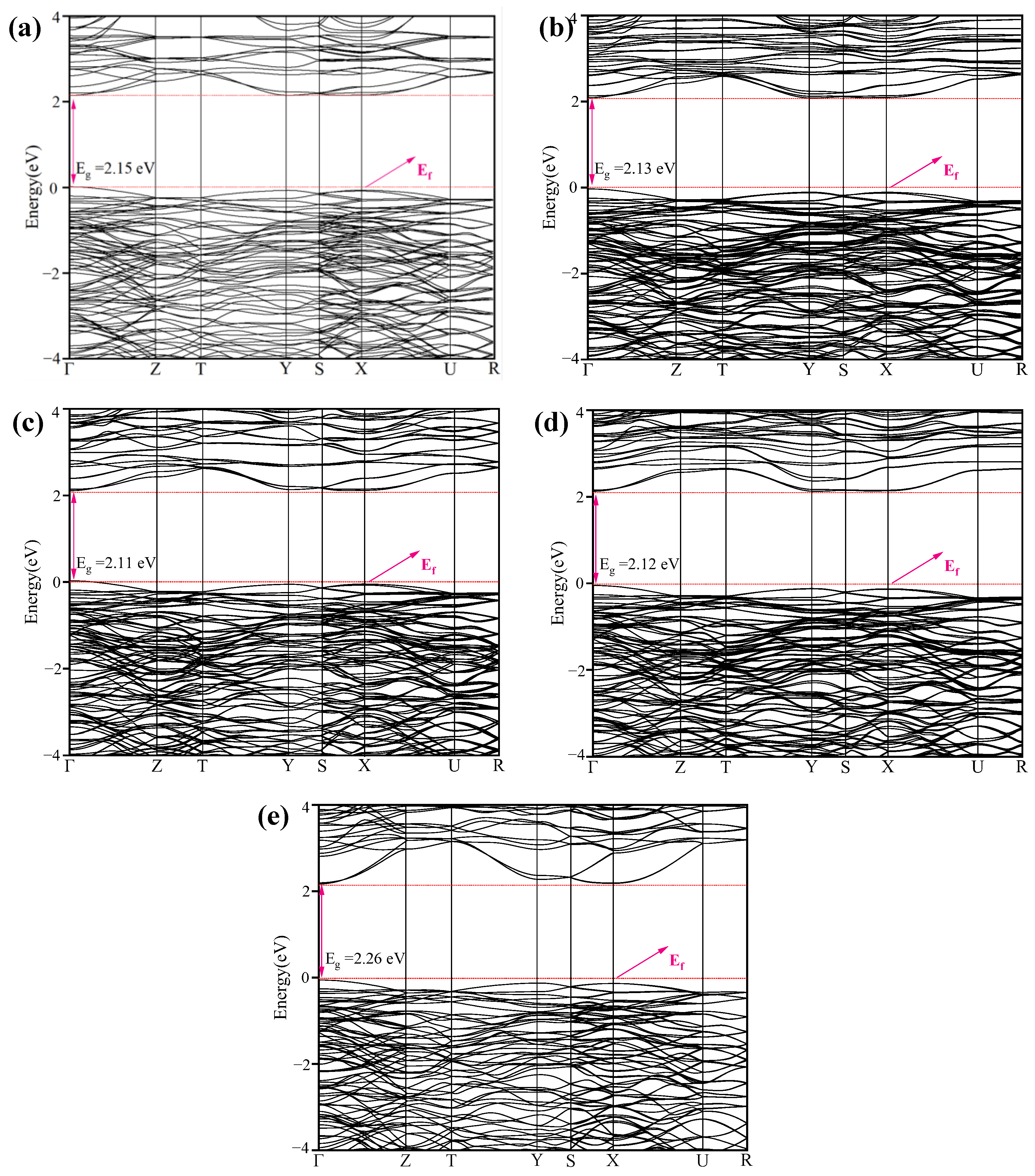
In the doping series, the Fermi energy levels of all five structures are located within the band gap, with the band gap remaining almost constant between 2.11 and 2.26 eV (Figure 3 and Figure S3), confirming their non-metallic properties. This suggests that W doping primarily regulates the position of the energy band edges while maintaining the overall electronic structure. Table 2 shows a clear trend in the band gaps of the five structures: the experimental values [31] are the largest, the known DFT results [32] are the smallest, and our calculations fall between these values. A consistent trend is evident: the band gap values for BMO (2.15 eV) and BWO (2.25 eV) calculated in this study lie between the higher experimental values (≈2.72 eV, 2.94 eV) and the lower previous DFT calculation results (1.90 eV, 1.98 eV). The observed differences arise from the known underestimation of the band gap by the GGA-PBE method and experimental factors. Nevertheless, the consistent trend across all samples allows us to clearly associate it with the concentration of W, distinguishing the intrinsic doping effect from external doping effects.

3.2.2. Density of Electronic States

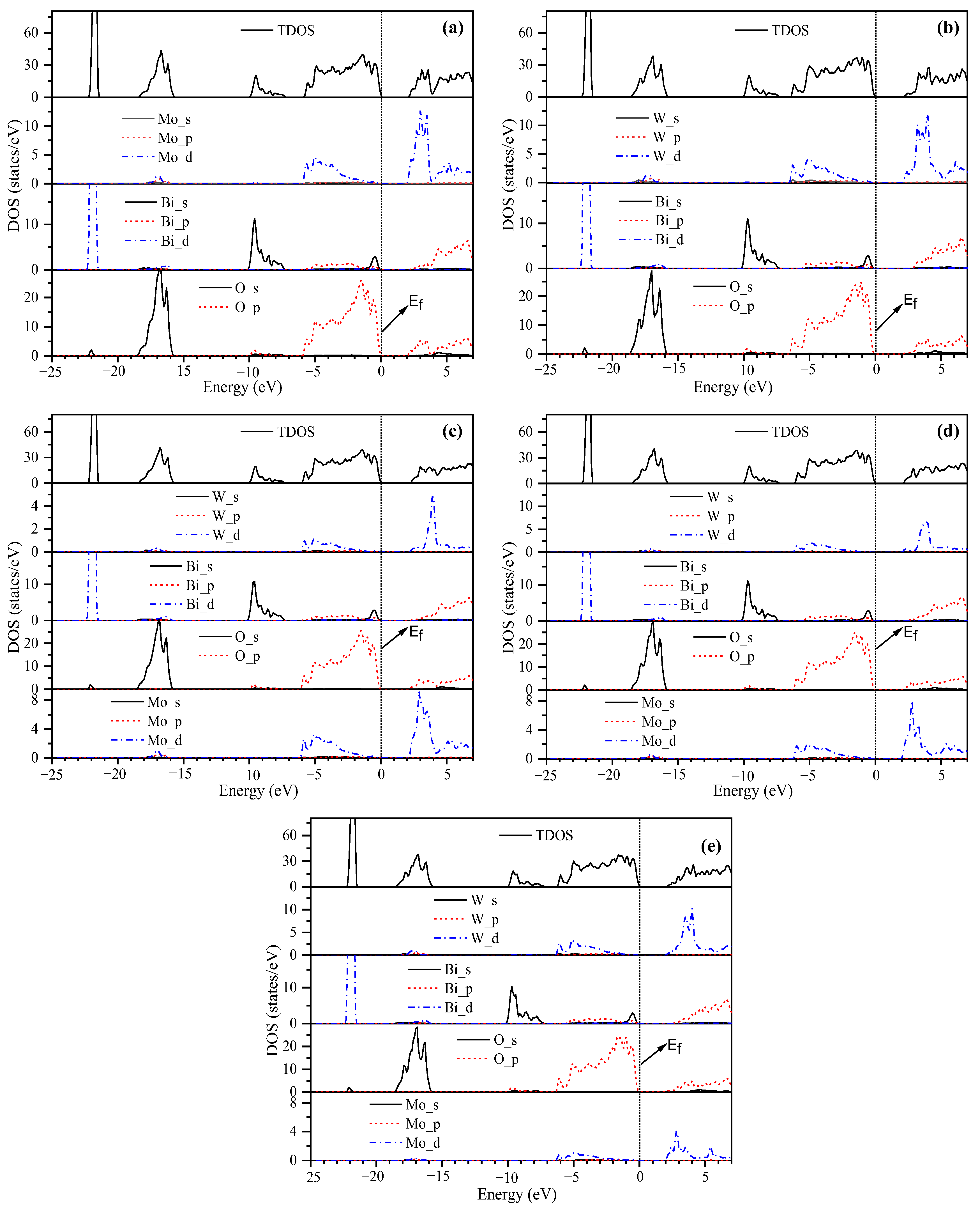
The electronic structure of this series of compounds (Figure 4) shows that the valence band maximum (VBM) is primarily composed of O 2p orbitals, while the conduction band minimum (CBM) is mainly composed of transition metal d orbitals. In γ-Bi2MoO6 (BMO), the conduction band consists primarily of Mo 4d orbitals, as shown by the projected density of states (DOS), with the Mo 4d orbitals contributing significantly to the CBM. However, doping with tungsten (W) results in the dominant transformation of the CBM to W 5d orbitals, with this transformation directly proportional to the concentration of W. At a doping concentration of x = 0.25, the contribution of Mo 4d orbitals to the CBM is approximately 75%, while W 5d orbitals contribute about 25%. As the doping concentration increases to x = 0.75, the contribution of W 5d orbitals to the CBM increases to 75%, significantly altering the conduction band structure. At this higher doping concentration, both Mo 4d and W 5d orbitals appear and rearrange near the band edges. The changes in the band gap are driven by the evolution of hybridization between these orbitals, and the band gap range of this series of materials remains narrow (2.11–2.26 eV), as shown in the calculation results [33]. The non-monotonic band gap response to W doping—initial narrowing followed by widening—results from energy shifts in Mo/W–d states near the CBM [34]. W doping preserves the O 2p-dominated VBM; so, the overall band structure remains relatively unchanged. In contrast, the conduction band states shift more significantly, which best explains the trends in photoexcited carrier behavior and catalytic performance [35].

3.2.3. Electron Localization Function

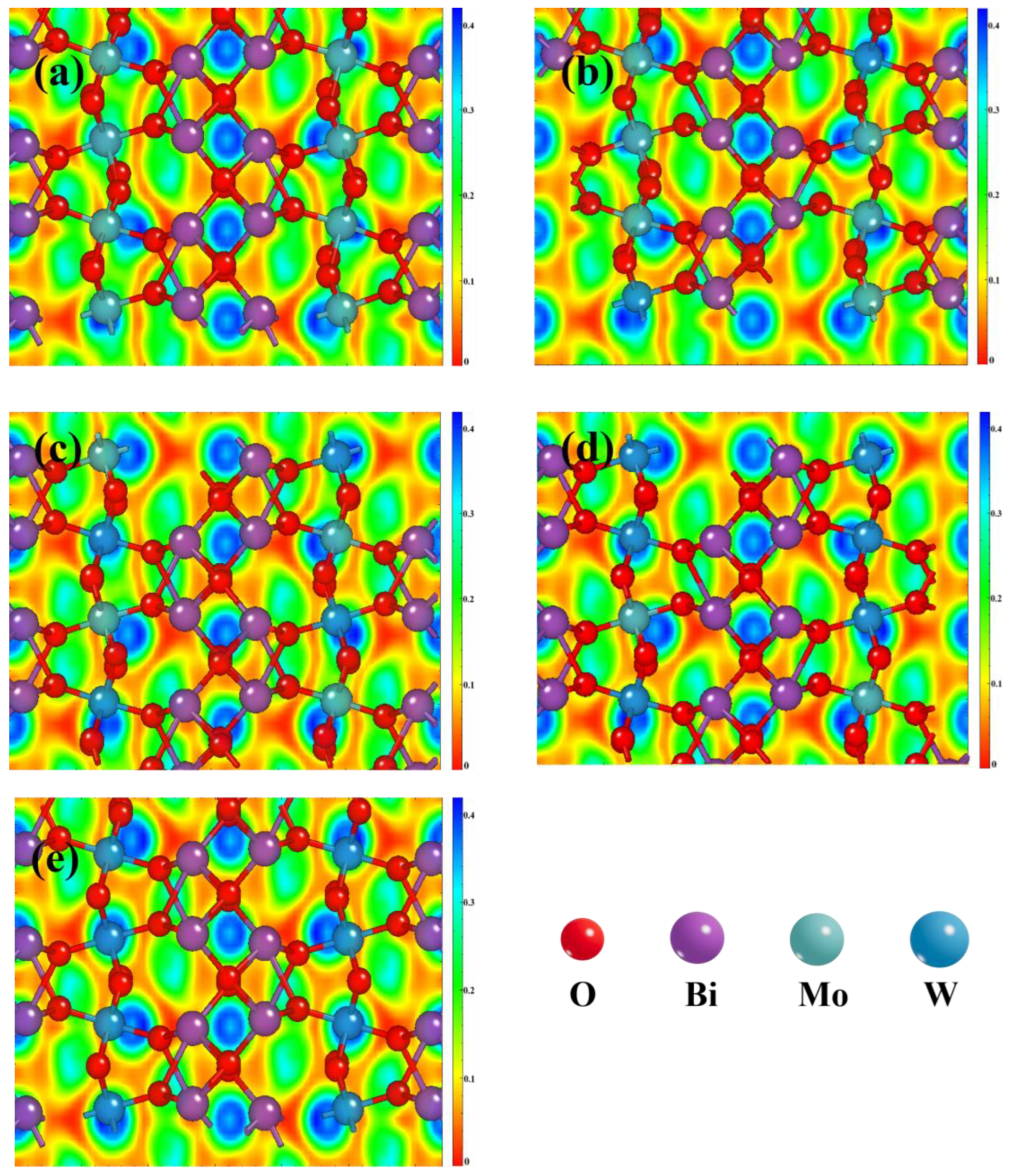
The electron localization function (ELF) spectrum can accurately locate high electron density regions, so as to track the charge separation structure at the heterogeneous junction and the charge transfer path at the interface [36,37]. The ELF analysis of the γ-Bi2MoO6 series (Figure 5) visualizes the charge redistribution caused by doping. These graphs reveal the changes in the electron density in real space caused by W substitution. Red and blue mark the high localization and low localization regions, respectively. Stronger localization of electrons near oxygen atoms and the dominance of O 2p orbitals at the top of the valence band (VBM) indicate that local electrons mainly come from the energy state derived from O.
W doping will specifically change the ELF in the (Mo/W)–O bonding region; these local adjustments cause the whole series of ELF patterns to become more and more similar under high doping levels, without defect states or long-range transfer paths. As a result, the material does not show metallic behavior. W substitution mainly affects the (Mo/W)–O bonding, but the change is small. The high-ELF regions still stay near oxygen sites. Their shape and strength shift only slightly in the nearby area. The results show that W doping changes d–p mixing, slightly distorts the local lattice, and shifts the local charge density [38,39]. The real-space results agree with the electronic-structure analysis and show only a small band-gap change. The DOS shows the same trend: the CBM gradually moves from Mo 4d to W 5d as the doping level increases. W doping causes only modest shifts at the band edges and in local bonding; so, the material remains semiconducting. The change looks like a fine adjustment of the electronic structure, not a major rework.

3.3. Optical Structure Information

We use the complex dielectric function ε(ω) (Equation (1)) to evaluate the optical response, in which the virtual part ε2(ω) represents the inter-band transition, and the real part ε1(ω) is derived from ε2(ω) through the Kramers–Kronig relationship. According to ε(ω), we calculated the complex refractive index (Equation (2)) and obtained the absorption coefficient α(ω), reflectance R(ω) and the energy loss function L(ω) (Equations (3)–(9)).
ε ( ω ) = ε 1 ( ω ) + i ε 2 ( ω )
N ( ω ) = ε ( ω ) = n ( ω ) + i κ ( ω )
ε 1 ( ω ) = 1 + 2 π P 0 ε 2 ( ω ) ω ω 2 ω 2 d ω
ε 2 ( ω ) = e 2 ω 2 π m 2 v , c BZ d k Ψ c k | e ^ p | Ψ v k 2 δ E c ( k ) E v ( k ) ω
n ( ω ) = ε 1 2 ( ω ) + ε 2 2 ( ω ) + ε 1 ( ω ) 2 1 2
κ ( ω ) = ε 1 2 ( ω ) + ε 2 2 ( ω ) ε 1 ( ω ) 2 1 2
R ( ω ) = κ 2 ( ω ) + 1 n ( ω ) 2 κ 2 ( ω ) + 1 + n ( ω ) 2
α ( ω ) = 2 ω κ ( ω ) c = 4 π κ ( ω ) λ 0
L ( ω ) = Im 1 ε ( ω ) = ε 2 ( ω ) ε 1 2 ( ω ) + ε 2 2 ( ω )

3.3.1. Complex Dielectric Constant

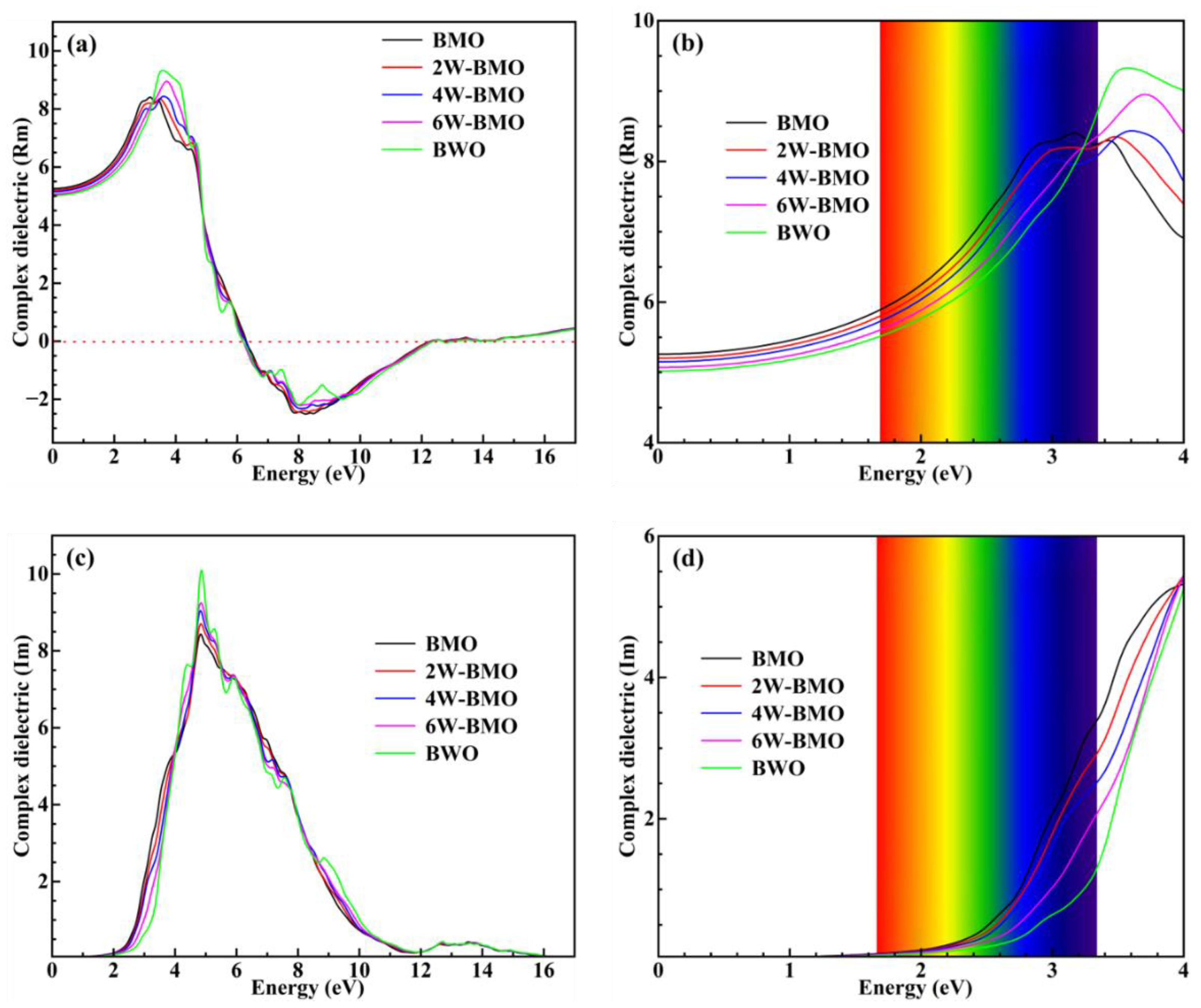
Looking at the complex dielectric function, we see that the optical response is quite consistent across the W-doped series. As shown in Figure 6a,b, the real part, ε1(ω), shows a similar static dielectric constant (around 5) at low energies, which points to noticeable dispersion near the absorption edge. As the energy increases (around 6 eV), ε1(ω) drops sharply and even goes negative—this is a clear sign of plasma dispersion linked to strong interband transitions. The dielectric response changes to metal behavior above 6 eV (ε1 < 0), indicating that the plasma excitation element is excited; and the rise of ε2(ω) near 2 eV is consistent with the calculated band gap (Figure 6c,d). This consistency is reflected in the small offset of the optical absorption edge after W doping. The main optical change is the offset of the absorption starting point, while the band gap remains almost unchanged. All samples showed strong 4–7 eV absorption peaks, and their positions were not shifted after W doping [40]. Projected state density (DOS) shows that the valence band top (VBM) is mainly composed of the O 2p state, and the guide band (CB) is mainly composed of the (Mo/W) d state; therefore, the strong absorption peak at 4–7 eV is attributed to the interband jump between the two [41,42,43]. W doping changes the dispersion at the starting point of absorption and the visible light range, which is mainly due to the increase in W d orbitals contribution and the change in d-p hybridization near the band. These adjustments fine-tune the spectral contour while maintaining the basic inter-band transition.

3.3.2. Reflectivity and Absorption Coefficient

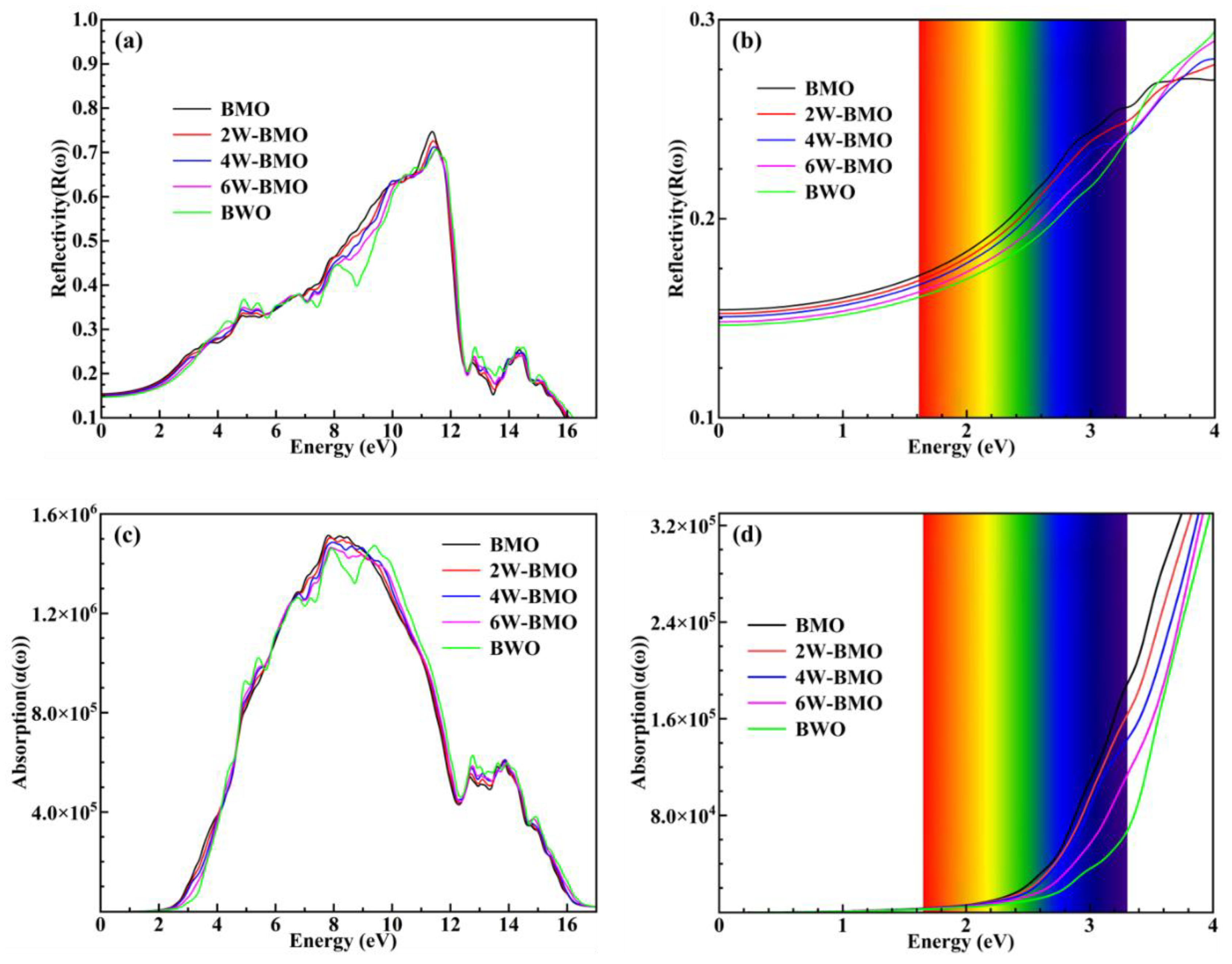
As shown in Figure 7a,b, the reflectance R(ω) of all the samples increases slowly with photon energy at first, then spikes in the middle range, and finally drops off in the high-energy region, showing some secondary fluctuations. In the visible range (~1.65–3.1 eV), reflectance stays low (0.12–0.30) and increases gradually. Here, pristine BMO shows the highest reflectance, whereas the W-doped samples remain lower. The reflectance of pure BWO is low in the infrared-visible light range, and there is only a significant increase at the ultraviolet absorption edge. In contrast, W doping has almost no effect on low-energy reflectivity. The starting point of absorption is located around 2 eV (Figure 7c,d), which matches the optical band gap. The doping causes a very small offset, which is consistent with the narrow absorption band range of 2.11–2.26 eV. Above the absorption edge, α(ω) rises sharply in the entire visible light range and reaches about 106 cm−1 above 5 eV. The spectrum shows a clear peak at 8–10 eV, which points to strong interband transitions. The band structure and DOS suggest that this absorption mainly comes from O 2p → (Mo/W) d transitions [44,45,46]. In the visible range, W doping mainly affects the spectrum near the band edges by changing d–p hybridization and the strength of interband transitions. As a result, the absorption profile changes slightly.

4. Conclusions

Density functional theory was applied to investigate how W doping affects the structural stability, electronic states at the band edges, and optical properties of γ-Bi2MoO6. The results show that, within the doping levels tested, replacing Mo with W maintains the stability of the Aurivillius-type layered structure, though it introduces some local distortions that are not disruptive. The lattice exhibits some anisotropic changes, but the overall structure is preserved, which is consistent with the predictions of our supercell substitution model. Electronically, all doped systems maintain semiconductor characteristics. Their band gaps show only slight fluctuations in the range of 2.11 to 2.26 eV. This indicates that doping primarily affects band-edge electronic states, rather than altering the intrinsic band structure. Density of state calculations show the valence band maximum dominated by O-2p orbitals, and Mo-4d and W-5d dominating the conduction band minimum. As the W content rises, the conduction band minimum gradually changes toward W-5d domination, achieving continuous modulation of the electronic states at the conduction band edge. Electron localization function analysis shows that W doping induces no metallic character. For W doping, its gradual modulation effect lies in the polarization of local (Mo/W)–O bonds and the strength of d–p hybridization, providing a structural basis for the evolution of band edges. Optical calculations also show that different doping models exhibit similar primary response mechanisms, and the absorption onset closely matches the band gap. It is found that W doping does not change the semiconductor framework, and enables the fine tuning of the visible absorption edge position and intensity. W doping adjusts the local coordination environment and reshapes the band-edge electronic states, which affects the visible-light absorption and controls the electronic structure and optical response. These findings provide a solid foundation for the doping design and performance optimization of Bi2MoO6-based layered oxide photocatalysts, and help us understand and optimize their performance from the atomic level.

Supplementary Materials

The following supporting information can be downloaded at: https://www.mdpi.com/article/10.3390/coatings16030338/s1, Figure S1. Total energy convergence with respect to k-point mesh; Figure S2. Total energy convergence with respect to the cutoff energy; Figure S3. (a) Band structure of BMO; (b) Band structure of BMO with 2W doping; (c) Band structure of BMO with 4W doping; (d) Band structure of BMO with 6W doping; (e) Band structure of BWO. The energy range shown is from −10 eV to +10 eV; Table S1. Bond lengths (Å) of M-O and W-O as a function of W doping concentration.

Author Contributions

Conceptualization, F.Z.; formal analysis, X.C. and Y.P.; methodology, Y.C. and X.G.; visualization, S.L. and S.X. (Shiheng Xin); writing—original draft, N.D.; writing—review and editing, F.Z. and S.X. (Suqin Xue). All authors have read and agreed to the published version of the manuscript.

Funding

This research was funded by the postgraduate research opportunities program of HZWTECH (HZWTECH-PROP).

Institutional Review Board Statement

Not applicable.

Informed Consent Statement

Not applicable.

Data Availability Statement

Data are contained within this article.

Conflicts of Interest

The authors declare no conflicts of interest.

References

  1. Rasheed, T.; Bilal, M.; Nabeel, F.; Adeel, M.; Iqbal, H.M. Environmentally-Related Contaminants of High Concern: Potential Sources and Analytical Modalities for Detection, Quantification, and Treatment. Environ. Int. 2019, 122, 52–66. [Google Scholar] [CrossRef]
  2. Kumar, R.; Sudhaik, A.; Raizada, P.; Hosseini-Bandegharaei, A.; Thakur, V.K.; Saini, A.; Saini, V.; Singh, P. An Overview on Bismuth Molybdate Based Photocatalytic Systems: Controlled Morphology and Enhancement Strategies for Photocatalytic Water Purification. J. Environ. Chem. Eng. 2020, 8, 104291. [Google Scholar] [CrossRef]
  3. Nie, L.; Mei, D.; Xiong, H.; Peng, B.; Ren, Z.; Hernandez, X.I.P.; DeLaRiva, A.; Wang, M.; Engelhard, M.H.; Kovarik, L.; et al. Activation of Surface Lattice Oxygen in Single-Atom Pt/CeO2 for Low-Temperature CO Oxidation. Science 2017, 358, 1419–1423. [Google Scholar] [CrossRef] [PubMed]
  4. Bahnemann, D. Photocatalytic Water Treatment: Solar Energy Applications. Sol. Energy 2004, 77, 445–459. [Google Scholar] [CrossRef]
  5. Ning, J.; Zhang, B.; Siqin, L.; Liu, G.; Wu, Q.; Xue, S.; Shao, T.; Zhang, F.; Zhang, W.; Liu, X. Designing Advanced S-scheme CdS QDs/La-Bi2WO6 Photocatalysts for Efficient Degradation of RhB. Exploration 2023, 3, 20230050. [Google Scholar] [CrossRef] [PubMed]
  6. Li, Y.; Kong, X.; Bao, R.; Liu, L.; Ge, Z.; Liu, F.; Cui, H.; Yi, J. Robust Oxygen Vacancy Surfaces Induce Chemical Bonding Interfaces of Bi2Sn2O7/Bi2MoO6 S-Scheme Heterojunction with Asymmetric Adsorption Sites for Efficient Photocatalytic Nitrogen Fixation. Chem. Eng. J. 2026, 531, 173870. [Google Scholar] [CrossRef]
  7. Xiong, Z.; Zhang, H.; Zhang, W.; Lai, B.; Yao, G. Removal of Nitrophenols and Their Derivatives by Chemical Redox: A Review. Chem. Eng. J. 2019, 359, 13–31. [Google Scholar] [CrossRef]
  8. Zhang, B.; Fang, C.; Ning, J.; Dai, R.; Liu, Y.; Wu, Q.; Zhang, F.; Zhang, W.; Dou, S.; Liu, X. Unusual Aliovalent Cd Doped γ-Bi2MoO6 Nanomaterial for Efficient Photocatalytic Degradation of Sulfamethoxazole and Rhodamine B under Visible Light Irradiation. Carbon Neutralization 2023, 2, 646–660. [Google Scholar] [CrossRef]
  9. Lyu, M.; Wang, C.; Rong, Y.; Wei, J.; Yang, Y.; Liu, Y.; Wei, G.; Zhang, Q.; Wang, C.; Xiu, J. Advances in Modification of Bi2MoO6 and Its Photocatalysis: A Review. J. Alloys Compd. 2024, 982, 173759. [Google Scholar] [CrossRef]
  10. He, R.; Xu, D.; Cheng, B.; Yu, J.; Ho, W. Review on Nanoscale Bi-Based Photocatalysts. Nanoscale Horiz. 2018, 3, 464–504. [Google Scholar] [CrossRef]
  11. Ma, W.; Gao, J.-H.; Wang, W.-T.; Qi, S.; Chen, T.; Zhou, Y.-M.; Tan, H.-Z.; Diao, J.-F.; Jing, K.-Q.; Wu, L. Enhancing Photothermal Selective Oxidation Performance of Benzyl Alcohol on Hierarchical Bi2MoO6 Spheres with In-Situ Oxygen Vacancy Modulation via Photothermal Induced Defect Engineering. Appl. Catal. A Gen. 2025, 708, 120575. [Google Scholar] [CrossRef]
  12. Xue, J.; Xiao, W.; Shi, L.; Liu, Y.; Wang, P.; Bi, Q. Efficient Degradation of Ciprofloxacin by a Flower-Spherical Bi2MoO6/BiOCl Z-Type Heterojunction Photocatalyst Enriched with Oxygen Vacancies. J. Environ. Chem. Eng. 2023, 11, 111235. [Google Scholar] [CrossRef]
  13. Xu, Q.; Sun, F.; Liu, X.; Hu, Y.; Luo, C.; Wang, X.; Shao, H.; Yu, H.; Yu, W.; Dong, X. Upconverting Luminescence and Surface Plasmon Resonance Synergistically Boost Photocatalytic Activity of LaOCl: Yb3+, Er3+/Bi2MoO6/Ag Nanofiber S-Scheme Heterojunction Photocatalyst for Degradation of Organic Contaminants. J. Alloys Compd. 2025, 1020, 179363. [Google Scholar] [CrossRef]
  14. Yang, C.; Zhang, Y.; Yue, F.; Du, R.; Ma, T.; Bian, Y.; Li, R.; Guo, L.; Wang, D.; Fu, F. Co Doping Regulating Electronic Structure of Bi2MoO6 to Construct Dual Active Sites for Photocatalytic Nitrogen Fixation. Appl. Catal. B Environ. 2023, 338, 123057. [Google Scholar] [CrossRef]
  15. Han, B.; Zhang, J.; Li, P.; Li, J.; Bian, Y.; Shi, H. Synthesis and Luminescence Properties of Eu3+ Doped High Temperature Form of Bi2MoO6. J. Electron. Mater. 2015, 44, 1028–1033. [Google Scholar] [CrossRef]
  16. Yu, Z.; Zhang, C.; Lou, X.; Zuo, R.; Yang, Y.; Jia, G. Rare Earth Ions Doped Bi2MoO6 Luminescent Materials: Pechini Sol-Gel Synthesis, down-Conversion and up-Conversion Multicolor Emissions, and Potential Applications. Ceram. Int. 2023, 49, 25987–25997. [Google Scholar] [CrossRef]
  17. Li, X. Design of Carbon Nitride-Based Materials for Highly Efficient Visible-Light Driven Photocatalysis. PhD Thesis, RMIT University, Melbourne, Australia, 2023. [Google Scholar]
  18. Ma, T.; Yang, C.; Guo, L.; Soomro, R.A.; Wang, D.; Xu, B.; Fu, F. Refining Electronic Properties of Bi2MoO6 by In-Doping for Boosting Overall Nitrogen Fixation via Relay Catalysis. Appl. Catal. B Environ. 2023, 330, 122643. [Google Scholar] [CrossRef]
  19. Liu, D.; Yin, X.; Li, L.; Chen, C.; Lin, Q.-X.; Zhang, H.-X.; Liu, E.; Wang, J.-F. Bi2 MoO6/Bi2MoO6– x S-Scheme Homojunction for Efficient Photocatalytic N2 Reduction. Langmuir 2025, 41, 32838–32848. [Google Scholar] [CrossRef]
  20. Sharma, M.; Kumar, A.; Gill, D.; Jaiswal, S.; Patra, A.; Bhattacharya, S.; Krishnan, V. Boosting Photocatalytic Nitrogen Fixation via Nanoarchitectonics Using Oxygen Vacancy Regulation in W-Doped Bi2MoO6 Nanosheets. ACS Appl. Mater. Interfaces 2023, 15, 55765–55778. [Google Scholar] [CrossRef]
  21. Huang, X.; Du, R.; Ren, J.; Li, X.; Fu, M.; Fu, S.; Ma, T.; Guo, L.; Soomro, R.A.; Yang, C.; et al. Unveiling the Mechanism of Aerobic Photocatalytic Nitrogen Fixation over Dynamic Structural Renovation on Bi2MO6 (M = Mo, W). ACS Catal. 2024, 14, 13542–13549. [Google Scholar] [CrossRef]
  22. Zhai, R.; Yang, Y.; Lei, P.; Lu, J.; Chen, S.; Sun, X. The Development of Environmentally Friendly Pr/W Co-Doped Bi2MoO6 Green Pigment with High near-Infrared Reflectivity. Ceram. Int. 2024, 50, 49936–49946. [Google Scholar] [CrossRef]
  23. Cao, H.; Cao, Y.; He, J.; Xie, X.; Wang, Z.; Sun, S.; Zhong, R.; Sun, L.; Wang, Y.; Zhang, K. Modulating Band Structure of MoO3 via W-Doped for Enhanced Photo-Induced Charge Transfer and SERS Detection. Chem. Eng. J. 2025, 520, 166007. [Google Scholar] [CrossRef]
  24. Sha, H.; Wang, Q.; Huang, J.; Sun, X.; Wu, G.; Liu, Y.; Shen, W. Research of Tungsten-Doped Diamond: First-Principles Studies. J. Nucl. Mater. 2025, 617, 156158. [Google Scholar] [CrossRef]
  25. Zhao, L.; Zhou, Y.; Xu, X.; Bai, T.; Gao, J.; Ma, M.; Zhang, X.; Zhang, J.; Wang, L.; Zhang, Y. Local Electronic Structure Engineering and Carrier Dynamics Optimization in W-Doped ZnS for Efficient Photocatalytic CO2 Reduction. Chem. Eng. J. 2025, 525, 170371. [Google Scholar] [CrossRef]
  26. Blöchl, P.E. Projector Augmented-Wave Method. Phys. Rev. B 1994, 50, 17953–17979. [Google Scholar] [CrossRef] [PubMed]
  27. Hongzhiwei Technology. Device Studio, Version 2023A. Available online: https://cloud.hzwtech.com (accessed on 10 January 2026).
  28. Perdew, J.P.; Burke, K.; Ernzerhof, M. Generalized Gradient Approximation Made Simple. Phys. Rev. Lett. 1996, 77, 3865–3868. [Google Scholar] [CrossRef]
  29. Xie, Y.; Liu, D.; Wang, B.; Li, D.; Yan, Z.; Chen, Y.; Shen, J.; Zhang, Z.; Wang, X. Monolayer Bi2W1−xMoxO6 Solid Solutions for Structural Polarity to Boost Photocatalytic Reduction of Nitrobenzene under Visible Light. ACS Sustain. Chem. Eng. 2021, 9, 2465–2474. [Google Scholar] [CrossRef]
  30. Zhang, B.; Liu, G.; Shi, H.; Wu, Q.; Xue, S.; Shao, T.; Zhang, F.; Liu, X. Density Functional Theory Study of Electronic Structure and Optical Properties of Ln3+-Doped γ-Bi2MoO6 (Ln = Gd, Ho, Yb). Crystals 2023, 13, 1158. [Google Scholar] [CrossRef]
  31. Zhou, L.; Yu, M.; Yang, J.; Wang, Y.; Yu, C. Nanosheet-Based Bi2MoxW1−xO6 Solid Solutions with Adjustable Band Gaps and Enhanced Visible-Light-Driven Photocatalytic Activities. J. Phys. Chem. C 2010, 114, 18812–18818. [Google Scholar] [CrossRef]
  32. Murugan, C.; Soundarya Mary, A.; Murugan, P.; Pandikumar, A. Enhanced Photoelectrocatalytic Water Splitting in Bi2Mo1−xWxO6 Solid Solutions: Understanding the Atomic Level Mechanism from the Experimental and First-Principles Approach. ACS Appl. Energy Mater. 2023, 6, 8410–8421. [Google Scholar] [CrossRef]
  33. Ahmed, T.Y.; Aziz, S.B.; Dannoun, E.M.A. New Photocatalytic Materials Based on Alumina with Reduced Band Gap: A DFT Approach to Study the Band Structure and Optical Properties. Heliyon 2024, 10, e27029. [Google Scholar] [CrossRef]
  34. Zhou, X.; Liu, C.; Zhang, Z.; Chen, P.; Yang, Y.; Yang, S. Construction of Bismuth-Deposited Bi4O5Br2 Complex and Exploration of Its Photocatalytic Properties. J Mater. Sci. Mater. Electron. 2023, 34, 558. [Google Scholar] [CrossRef]
  35. Saroar, S.; Sultana, S.; Nishat, S.S.; Hossain, Q.S.; Khan, M.N.I.; Islam, D.; Akhtar, U.S.; Shahriar Bashar, M.; Jahan, S.; Hossain, K.S.; et al. First-Principles Calculations on Electronic, Optical, and Phonon Properties of γ-Bi2MoO6. ACS Omega 2024, 9, 36314–36325. [Google Scholar] [CrossRef]
  36. Zhao, B.; Xing, Y.; Xue, Y.; Chen, N.; Sun, C.; Li, M.; Shi, H.; Ma, B.; Wang, S.; Tang, Y. Efficient Degradation of Dye Wastewater with a Novel Tribocatalytic Process Initiated by CQDs-Bi2MoO6 Catalyst: Preparation, Degradation, Kinetics, DFT Calculations and Mechanism. Chem. Eng. J. 2025, 511, 161852. [Google Scholar] [CrossRef]
  37. Li, J.; Wang, Y.; Guo, Y.; Zhang, S.; Kuai, Y. Oxygen Vacancy Modulation of Bi2MoO6/C3N4 Heterojunction from Type-II to S-Scheme for Enhancing Photocatalytic H2 Evolution: A DFT Study. Colloids Surf. A Physicochem. Eng. Asp. 2025, 729, 138931. [Google Scholar] [CrossRef]
  38. Hao, C.; Dong, X.; Li, C.; Dong, C.; Yang, Z.; Yang, J. Structural Behaviors, Optical Properties and Electronic Structures of Rare Earth Samarium Doped Germanium Anion Nanocluster SmGen (n = 4–20): A Density Functional Theory Investigation. Mater. Sci. Eng. B 2025, 315, 118095. [Google Scholar] [CrossRef]
  39. Fayyadh, H.A. First-Principles Investigation of Concentration Effects on the Electronic and Vibrational Properties of a Boron Aluminum Phosphide Alloy with Wurtzoid Nanostructure. Ukr. J. Phys. 2022, 67, 750. [Google Scholar] [CrossRef]
  40. Sun, C.; Zhang, C.; Zhang, B. Adjusting the Structural, Electronic and Optical Properties of CdS by the Introduction of Be: A DFT Study. Mater. Today Commun. 2022, 31, 103394. [Google Scholar] [CrossRef]
  41. Mllaoiy, L.; Bikerchalen, S.; Bakiz, B.; Villain, S.; Taoufyq, A.; Guinneton, F.; Gavarri, J.-R.; Benlhachemi, A. Structure, Morphological, Electronic, and Optical Properties of Bi24O31Br10 Oxybromide Photocatalyst: A Combined Experimental Study and DFT Calculation. Mater. Sci. Eng. B 2026, 324, 119016. [Google Scholar] [CrossRef]
  42. Swapnalin, J.; Banerjee, P.; Sabbanahalli, C.; Rangappa, D.; Kondamareddy, K.K. Computational Techniques on Optical Properties of Metal-Oxide Semiconductors. In Optical Properties and Applications of Semiconductors; CRC Press: Boca Raton, FL, USA, 2022; pp. 155–166. [Google Scholar]
  43. Vu, T.V.; Luzhnyi, I.V.; Myronchuk, G.L.; Bekenev, V.L.; Bohdanyuk, M.S.; Lavrentyev, A.A.; Gabrelian, B.V.; Parasyuk, O.V.; Khyzhun, O.Y. DFT Calculations and Experimental Studies of the Electronic Structure and Optical Properties of Tl4PbI6. Opt. Mater. 2021, 114, 110982. [Google Scholar] [CrossRef]
  44. Qian, X.; Ma, Y.; Xia, X.; Xia, J.; Ye, J.; He, G.; Chen, H. Recent Progress on Bi4O5Br2-Based Photocatalysts for Environmental Remediation and Energy Conversion. Catal. Sci. Technol. 2024, 14, 1085–1104. [Google Scholar] [CrossRef]
  45. Wang, G.; Dou, K.; Cao, H.; Du, R.; Liu, J.; Tsidaeva, N.; Wang, W. Designing Z-Scheme CdS/WS2 Heterojunctions with Enhanced Photocatalytic Degradation of Organic Dyes and Photoreduction of Cr (VI): Experiments, DFT Calculations and Mechanism. Sep. Purif. Technol. 2022, 291, 120976. [Google Scholar] [CrossRef]
  46. Liang, Q.; Fan, J.; Deng, X.; Liu, J.; Zeng, J.; Zhang, H.; Li, J.; Liu, C.; Kang, Z.; Zhao, Z. Oxygen Vacancy-Driven Asymmetrical Charge Distribution on Bi-O-Sn Sites in Sn-Doped Bi2MoO6for Efficient Photocatalytic CO2-to-CH4 Conversion. Angew. Chem. 2026, 138, e21874. [Google Scholar] [CrossRef]
Figure 1. Structure model of W-doped BMO.
Coatings 16 00338 g001
Figure 2. Structural model of W-doped Bi2MoO6, (a) Pure BMO; (b) 0.25% W-doped BMO; (c) 0.50% W-doped BMO; (d) 0.75% W-doped BMO; (e) Pure BWO.
Coatings 16 00338 g002
Figure 3. (a) Band structure of BMO; (b) Band structure of BMO with 2W doping; (c) Band structure of BMO with 4W doping; (d) Band structure of BMO with 6W doping; (e) Band structure of BWO. The energy range shown is from −4 eV to +4 eV.
Coatings 16 00338 g003
Figure 4. (a) DOS and total DOS of BMO; (b) DOS and total DOS of BWO; (c) DOS and total DOS of BMO with 2W doping; (d) DOS and total DOS of BMO with 4W doping; (e) DOS and total DOS of BMO with 6W doping.
Coatings 16 00338 g004
Figure 5. (a) ELF of BMO; (b) ELF of W-doped BMO with 2W; (c) ELF of W-doped BMO with 4W; (d) ELF of W-doped BMO with 6W; (e) ELF of BWO.
Coatings 16 00338 g005
Figure 6. Complex dielectric function of each material: (a,b) real part and (c,d) imaginary part.
Coatings 16 00338 g006
Figure 7. Optical reflectivity and absorption spectra of W-doped BMO and BWO: (a) reflectivity spectra (0–16 eV); (b) Reflectivity spectra (0–4 eV); (c) absorption spectra (0–16 eV); (d) absorption spectra (0–4 eV).
Coatings 16 00338 g007
Table 1. Comparison of Lattice Parameters for Various Photocatalysts: Experimental (EXP) vs. DFT Results and Average Relative Error (%).
PhotocatalystsLattice Parameters [28]
(EXP)/(Å)
Lattice Parameters
(DFT)/(Å)
Average
Relative Error/(%)
abcabc
BMO5.51016.2765.5115.62016.5835.6382.06
0.25 W-BMO5.50616.3925.5095.63316.6235.6321.98
0.50 W-BMO5.49316.4185.5005.60216.6705.6261.94
0.75 W-BMO5.47916.4205.4795.59416.7175.6192.15
BWO5.46016.4255.4785.58516.765.6092.24
Table 2. Experimental result and DFT structure convergence result of band gap of BMO and W-BMO.
PhotocatalystsBand Gap [31] (EXP)
/(eV)
Band Gap (DFT) [32]/(eV)Band Gap (Our DFT)
/(eV)
BMO2.721.902.15
0.25 W-BMO2.681.862.13
0.50 W-BMO2.701.882.11
0.75 W-BMO2.691.892.14
BWO2.941.982.25
Disclaimer/Publisher’s Note: The statements, opinions and data contained in all publications are solely those of the individual author(s) and contributor(s) and not of MDPI and/or the editor(s). MDPI and/or the editor(s) disclaim responsibility for any injury to people or property resulting from any ideas, methods, instructions or products referred to in the content.