Article

Precision-Tuned Magnetron Sputtering for High-Performance Metallized Copper Films

1
Key Laboratory of Green Fabrication and Surface Technology of Advanced Metal Materials, Ministry of Education, Anhui University of Technology, Ma’anshan 243002, China
2
School of Materials Science and Engineering, Anhui University of Technology, Ma’anshan 243002, China
*
Authors to whom correspondence should be addressed.
Coatings 2025, 15(9), 1089; https://doi.org/10.3390/coatings15091089
Submission received: 29 July 2025 / Revised: 9 September 2025 / Accepted: 12 September 2025 / Published: 17 September 2025

Abstract

In the present study, copper (Cu) films were deposited on polyethylene terephthalate (PET) substrates using direct-current (DC) magnetron sputtering technology. A systematic investigation was conducted on the effects of process parameters, such as target power, gas flow rate, and substrate temperature, on the microstructure and properties of copper films. The results showed that an increase in the target power resulted in enhanced film grain size, accompanied by a reduction in resistivity and an improvement in adhesion strength. Furthermore, resistivity increased monotonically with elevated gas flow rates, whereas the adhesion strength was found to achieve its maximum at a flow rate of 350 mL/min. In addition, substrate temperature variations had negligible influence on the film grain size and resistivity; nevertheless, the adhesion progressively decreased with increasing substrate temperature. A set of optimal parameters (3 kW, 350 mL/min, −15 °C) was determined based on the comprehensive evaluation of deposition efficiency, conductivity and adhesion performance. The Cu film prepared under these conditions exhibited low resistivity (8.37 × 10⁻⁸ Ω·m) and improved adhesion strength (166 gf/mm). Therefore, it is concluded that high performance of metallized Cu films could be achieved by fine-tuning deposition parameters.

1. Introduction

Driven by the growing global demand for clean energy, sectors such as new energy vehicles, electronic equipment, and photovoltaic power generation are experiencing robust development. Against this backdrop, metallized Cu film, characterized by its unique Cu-polymer-Cu sandwich structure and significant technical advantages, has emerged as a key material in these applications. It is fabricated by depositing Cu layers onto both sides of a polymer substrate, retaining the excellent electrical conductivity of traditional Cu foil while achieving weight reduction and enhanced flexibility. When serving as the anode current collector in lithium-ion batteries, metallized Cu film not only enlarges energy density but also improves safety and cycling life [1]. In flexible circuit devices, it is employed as a flexible copper-clad laminate (FCCL), providing essential support for 5G equipment by enabling lower dielectric loss and miniaturization [2].
Currently, polyimide (PI), polyethylene terephthalate (PET), and polypropylene (PP) are commonly employed as polymer substrates for metallized Cu films. Among these, PI exhibits outstanding thermal stability and mechanical strength [3]; however, its relatively high cost hinders widespread adoption. While PP demonstrates promising potential due to advantages such as low density and excellent corrosion resistance, its practical application is restricted by the relatively low melting point, inferior tensile strength and poor toughness. In contrast, PET is considered the optimal substrate material owing to its moderate cost and favorable comprehensive performance.
At present, the predominant methods for preparing metallized Cu films encompass magnetron sputtering, vacuum evaporation, electroless plating and electroplating [4,5,6,7]. Significant research efforts have been made to enhance the performance of metallized Cu films. For instance, Huang et al. [8] significantly improved the adhesion of electroless plated Cu films on PET substrates by introducing a 6% SiO2-prime layer to enhance the substrate wettability. In addition, Hu et al. [9] prepared a silver layer on PI films by wet-chemical process prior to Cu electroplating. Ag agglomeration acted as a bridge between the Cu layer and PI, substantially increasing the interfacial bonding strength. However, these chemical-based approaches often involve complex procedures and multiple chemical reagents, raising concerns regarding environmental impact and safety. In another approach, Wang et al. [10] employed vacuum evaporation to deposit Cu films on PP substrates, achieving films with a high specific surface area that effectively reduced battery interfacial resistance. Nevertheless, a significant drawback is that the high evaporation temperature of Cu considerably exceeds the melting point of common polymer substrates, posing a risk of thermal damage to polymers during deposition. In contrast, magnetron sputtering has been widely applied for the fabrication of metallized Cu films due to its attractive advantages, including minimal substrate thermal damage, strong interfacial bonding, and suitability for industrial production [11].
Despite the significant advantages of magnetron sputtering for preparing metallized Cu films, optimizing interfacial adhesion and conductivity remains a significant industry challenge. Based on the Thornton model [12,13], it is known that the deposition parameters during the magnetron sputtering process, such as target power, working pressure and substrate temperature significantly influence the film microstructure and properties. However, for the fabrication of metallized Cu films, process design in industry still relies heavily on empirical knowledge, lacking systematic and in-depth research. Therefore, in this study, Cu films were deposited on PET substrates using direct-current (DC) magnetron sputtering. A systematic investigation was conducted to study the influence of critical process parameters, specifically sputtering power, working pressure, and substrate temperature, on the conductivity of the Cu films. In addition, a peel test was employed to quantitatively evaluate the effect of these process parameters on the adhesion strength of the Cu films. This study aims to provide both a theoretical foundation and experimental data for optimizing the deposition process of metallized Cu films.

2. Film Deposition and Characterization

2.1. Film Deposition

In this study, Cu films were deposited using a roll-to-roll DC magnetron sputtering system (RC × 300 × 350, Guangdong Zhenhua Technology Co., Ltd., Guangdong, China). Concerning the schematic diagram of the facility, please refer to the reference [14]. Polyethylene terephthalate (PET, Suzhou Dongxuan Plastics Products Co., Ltd., Suzhou, China) with the thickness of 50 μm was selected as the substrate. Additionally, to facilitate film thickness measurement, single-crystal Si (100) wafers (Kaihua Lijing Electronics Co., Ltd., Quzhou, China, approximately 650 μm thick) were also used as the substrate. A high-purity Cu sheet (Beijing Tianqi Advanced Materials Co., Ltd., Beijing, China, 99.99% purity) with the size of 550 mm × 120 mm was employed as the target. The PET substrates were cleaned ultrasonically in anhydrous ethanol (Sinopharm Chemical Reagent Co., Ltd., Shanghai, China), rinsed with deionized water made by a pure water system (CX-SH-20, Suzhou, China) and subsequently dried. The cleaned substrates were closely attached to the center of the cooling roll. The Target-to-Substrate distance was 75 mm. Prior to deposition, the chamber was evacuated to a base pressure of 2 × 10⁻³ Pa. Pure argon gas was then introduced into the chamber at a flow rate of 600 mL/min, and the Cu target was pre-sputtered at the power of 2 kW for five minutes to remove surface oxides and contaminants. Subsequently, the cooling roll was rotated to position the substrate directly facing the target, and Cu film deposition was initiated. The rotation speed of the cooling roll was 2 r·min−1, other specific experimental parameters are listed in Table 1. To enhance the readability of the table, the process parameters were categorized into five series. Sample IDs common to multiple series were highlighted in bold for distinction, such as sample 3#, 9# and 10#.

2.2. Film Characterization

The surface morphology of Cu films was characterized using field emission scanning electron microscopy (FE-SEM, Hitachi Regulus 8230, Tokyo, Japan), and the topography as well as surface roughness of Cu films were analyzed by atomic force microscopy (AFM, Bruker Icon, Billerica, MA, USA). Film thickness was determined using a surface profilometer (KLA-Tencor P7, Milpitas, CA, USA). The sheet resistance of Cu films was measured at room temperature using a four-point probe system (DMR-1C, Suzhou, China). The electrical conductivity was calculated using the following formula: ρ = R × d , where ρ denotes the conductivity, R represents the sheet resistance, and d is the film thickness. A peel test was conducted to quantitatively analyze the adhesion strength of the samples. The size of tested samples was approximately 15 mm × 150 mm. Prior to testing, the Cu-coated surface was thermally bonded to the ethylene-acrylic acid (EAA, Shenzhen FuJinFang Film Co., Ltd., Shenzhen, China) copolymer surface using an HS-H3 heat sealer (Saicheng Electronic Technology Co., Ltd., Jinan, China) under the following parameters: 300 kPa pressure, 20 s duration, and 85 °C temperature. Peeling strength was subsequently measured using a peel tester (BLD-200H, Saicheng Electronic Technology Co., Ltd., Jinan, China) with 100 mm displacement and 300 mm/min speed.

3. Results and Discussion

3.1. Effect of Sputtering Power

Figure 1 shows the thicknesses and deposition rates of Cu films prepared at various target powers (Samples 1#–5#). It can be seen that the thickness of Cu films increased linearly with the increase in target power, which was consistent with the results reported by Jin et al. [15]. This phenomenon was attributed to the enhanced plasma bombardment resulting from the increased target power. During the deposition process, an increased number of Cu atoms or clusters were sputtered from the target and deposited onto the substrate surface by the intensified plasma bombardment, thereby increasing the film thickness and deposition rate [16,17].
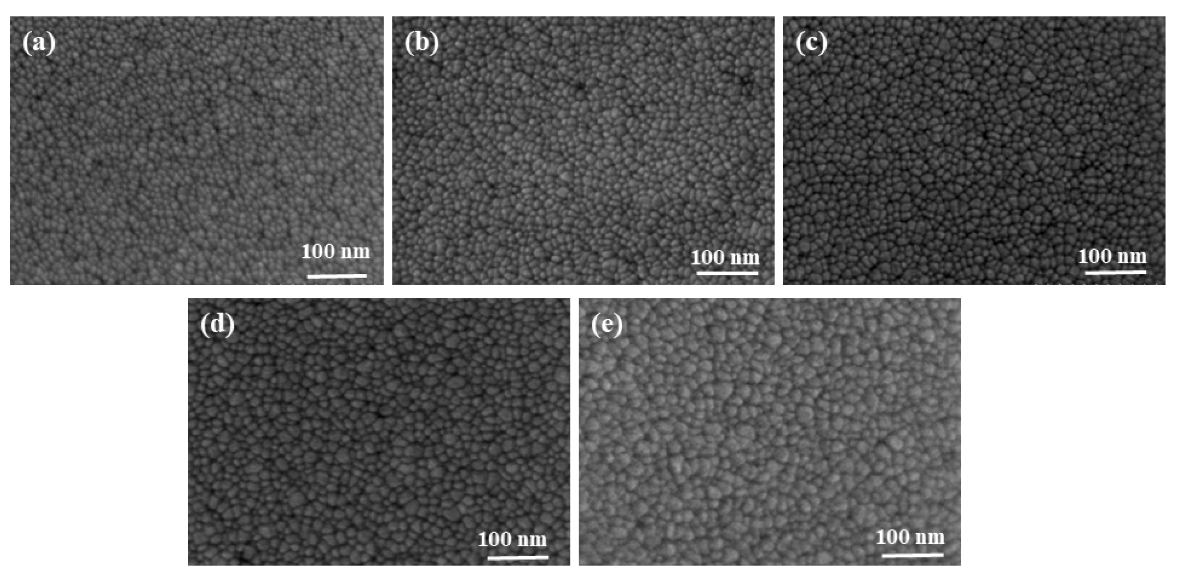
Figure 2 shows the SEM morphology of Cu films deposited at different target powers. To eliminate the effect of film thickness variations on the microstructure, Cu films with an identical thickness (approximately 80 nm) were fabricated by adjusting the deposition time (samples 3# and 6#–9#) As shown in Figure 2, Cu films exhibited a dense granular structure, and the grain size increased with the increase in sputtering power, which was also reported by Hu et al. [18]. Under lower sputtering power conditions, the energy of the deposited Cu clusters was limited, thus confining the diffusion of adatoms on the substrate surface. Consequently, cluster coalescence was restricted, leading to smaller grain sizes. In contrast, at relatively higher sputtering power, the energy of sputtered clusters was significantly enhanced, which enabled long-range diffusion of Cu adatoms, and cluster coalescence was promoted to reduce the Gibbs free energy, thereby yielding larger grains.
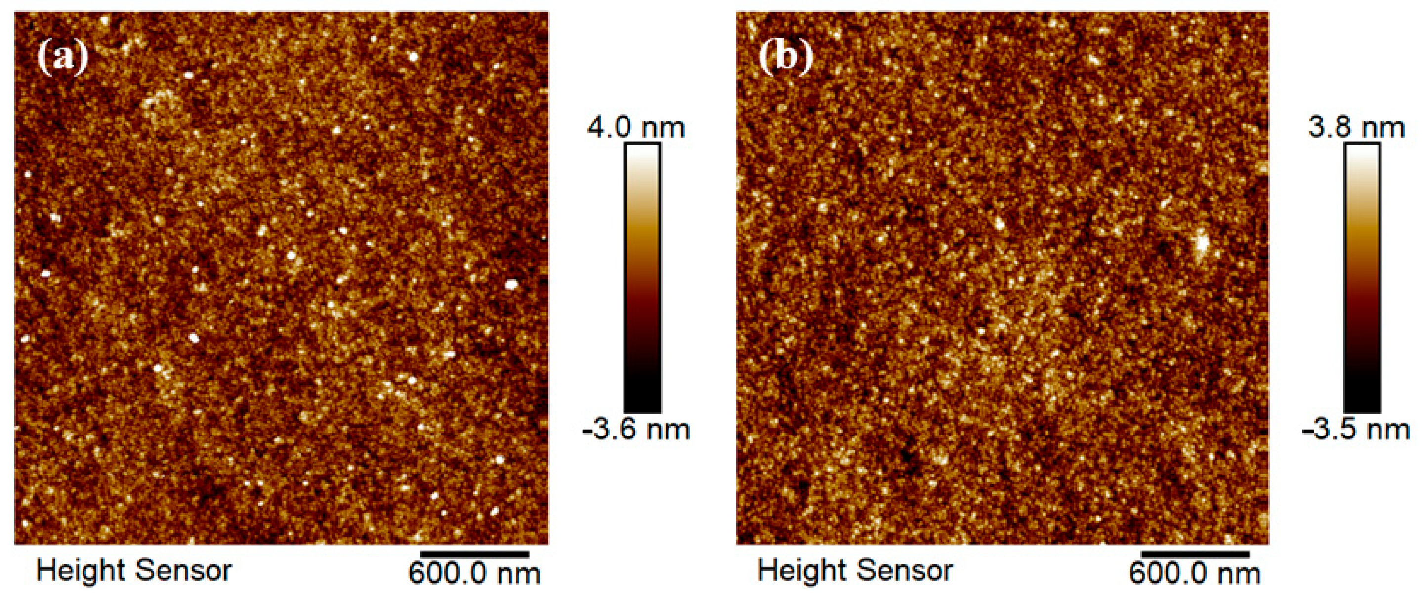
Figure 3 displays AFM topography of Cu films deposited at different sputtering powers, revealing that the particle size of Cu films increased with the target power (samples 6# and 9#). This trend corroborates the SEM observations in Figure 2. Le et al. [19] also demonstrated through AFM analysis that higher sputtering power promoted the Volmer-Weber growth mode, thus confirming its significant impact on film microstructure.
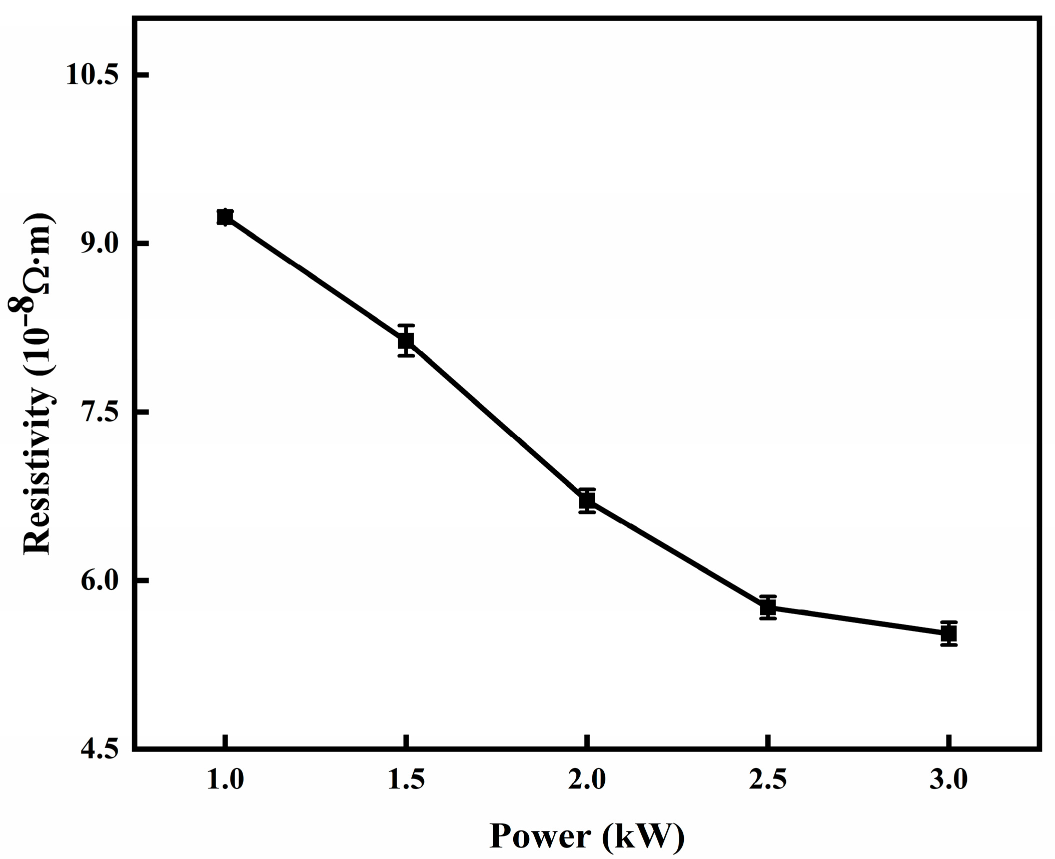
Figure 4 illustrates the resistivity of Cu films with a fixed thickness (~80 nm) deposited at various sputtering powers (samples 3# and 6#–9#). As the target power increased from 1 kW to 3 kW, the resistivity decreased monotonically, indicating enhanced electrical conductivity at higher target power.
With increasing sputtering power, the resistivity of Cu films exhibited a monotonic decrease. This phenomenon can be explained by the Fuchs-Sondheimer model [20,21]. According to this model, when the film thickness is larger than the average free path, the resistivity can be approximated as follows by Equation (1):
ρ t o t a l = ρ b o u n d a r y 1 + 3 λ 8 t ( 1 p )
where ρtotal denotes the total resistivity, ρboundary represents the additional resistivity from boundary scattering, t is the film thickness and p is the surface reflection coefficient (0 ≤ p ≤1). Lower p values means higher proportion of scattering, thereby elevating ρboundary. In addition, grain boundary scattering constitutes another critical mechanism [22]. Wang et al. [23] demonstrated in RF-sputtered Cu/Ta multilayers that when reducing sublayer thickness to 50–100 nm, the film resistivity was evaluated due to intensified grain boundary scattering. This occurs because grain boundary area A is inversely proportional to average grain diameter d, as follows by Equation (2):
A 1 d
The role of grain boundary scattering was described by the Mayadas-Shatzkes model [24], as follows by Equation (3):
ρ g r a i n = ρ i n t r i n s i c 1 + 3 2 β , β = λ d R 1 R
where ρgrain is the resistivity of polycrystalline film, ρintrinsic denotes the intrinsic resistivity of bulk Cu, R is the grain boundary reflection coefficient (0 ≤ R ≤ 1) and β parametrizes scattering intensity. As the sputtering power increases, the kinetic energy of Cu deposited particles rises significantly, which promotes the increase in grain size d, resulting in a decrease in β, thereby reducing the contribution of grain boundary scattering to resistivity.
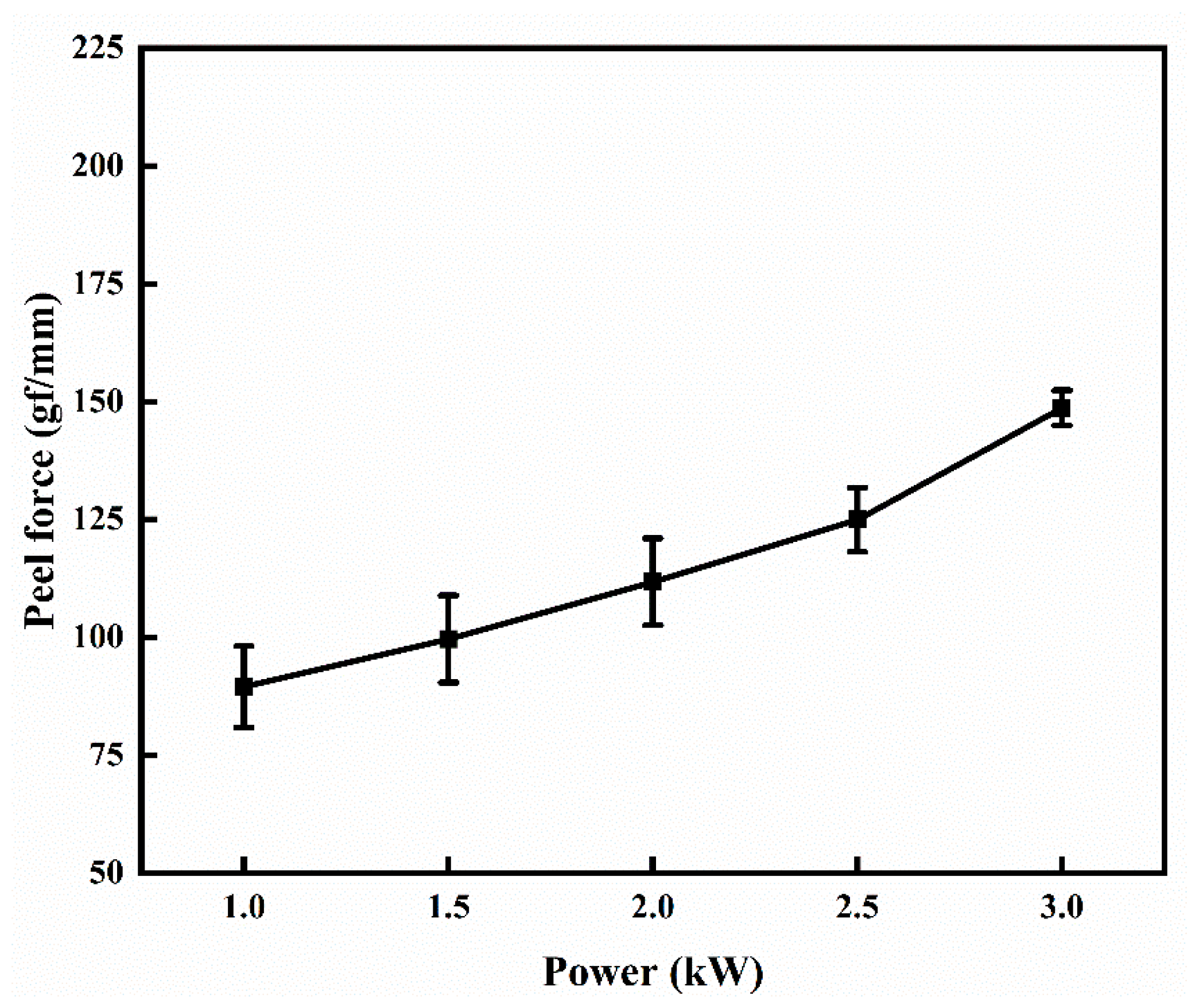
The peel test was employed to quantitatively evaluate the interfacial bonding strength between Cu films and PET substrates deposited at different sputtering powers. Figure 5 depicts the adhesion force as a function of sputtering power, revealing a monotonic increase in peel force from 1 kW to 3 kW (samples 3# and 6#–9#). This enhancement was attributed to two primary mechanisms: (1) the elevated particle energy at higher sputtering power facilitated deeper infiltration of Cu clusters into microscopic surface asperities of PET films, thereby increasing interfacial mechanical interlocking interaction; (2) the enhanced sputtering power promoted grain growth in Cu films (as confirmed by Figure 2 and Figure 3), which reduced grain boundary density and mitigated stress concentration at the interface [25], thereby strengthening chemical bonding at the Cu-PET interface.
At 3 kW sputtering power, the deposited Cu films exhibit optimal performance—characterized by dense microstructure, superior electrical conductivity, and maximum bonding strength.

3.2. Effect of Gas Flow Rate

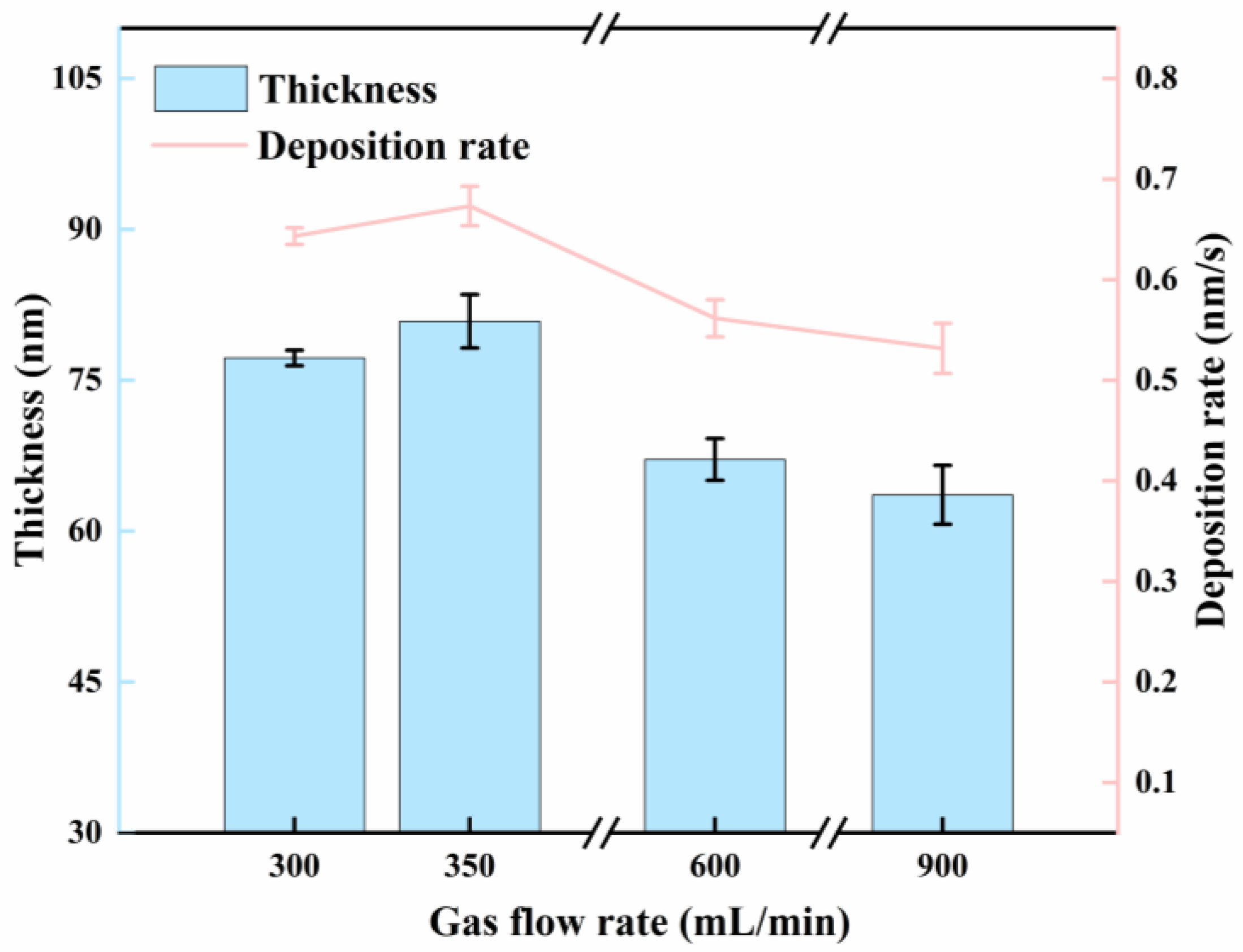
Figure 6 illustrates the variation in Cu film deposition rate as a function of gas flow rate (samples 9#–12#). The results indicated that the film thickness initially increased and subsequently decreased with increasing gas flow rate. The maximum deposition rate was observed at a gas flow rate of 350 mL/min (corresponding to a working gas pressure of 0.2 Pa), where the film thickness exceeded 80 nm. The mean free path of gas molecules is an important factor affecting the film deposition rate, which can be estimated by Equation (4) [26].
λ ¯ = k T 2 π D 2 p
where λ ¯ is the mean free path, k is the Boltzmann constant, T denotes the ambient temperature, D represents the collision cross-section radius, and p is the deposition gas pressure. At a gas flow rate of 300 mL/min, the mean free path of charged particles was relatively long. However, due to the low gas density within the chamber at this flow rate, the number of Ar+ ions generated was limited. Consequently, fewer high-energy charged particles bombarded the target surface, resulting in a low sputtering yield and a correspondingly low deposition rate. When the gas flow rate was increased to 350 mL/min, more energetic Ar+ ions bombarded the target surface, which resulted in a greater deposition efficiency. However, when the gas flow rate was further increased beyond this optimal point, the gas molecular density within the chamber was significantly elevated. This caused the collision probability between Ar particles, as well as between Cu particles and Ar particles, to be greatly increased. Consequently, the mean free path of charged particles was markedly shortened. As a result, both the kinetic energy of the sputtered Cu particles and their flux reaching the substrate surface were reduced, ultimately leading to a decrease in the deposition rate [27].
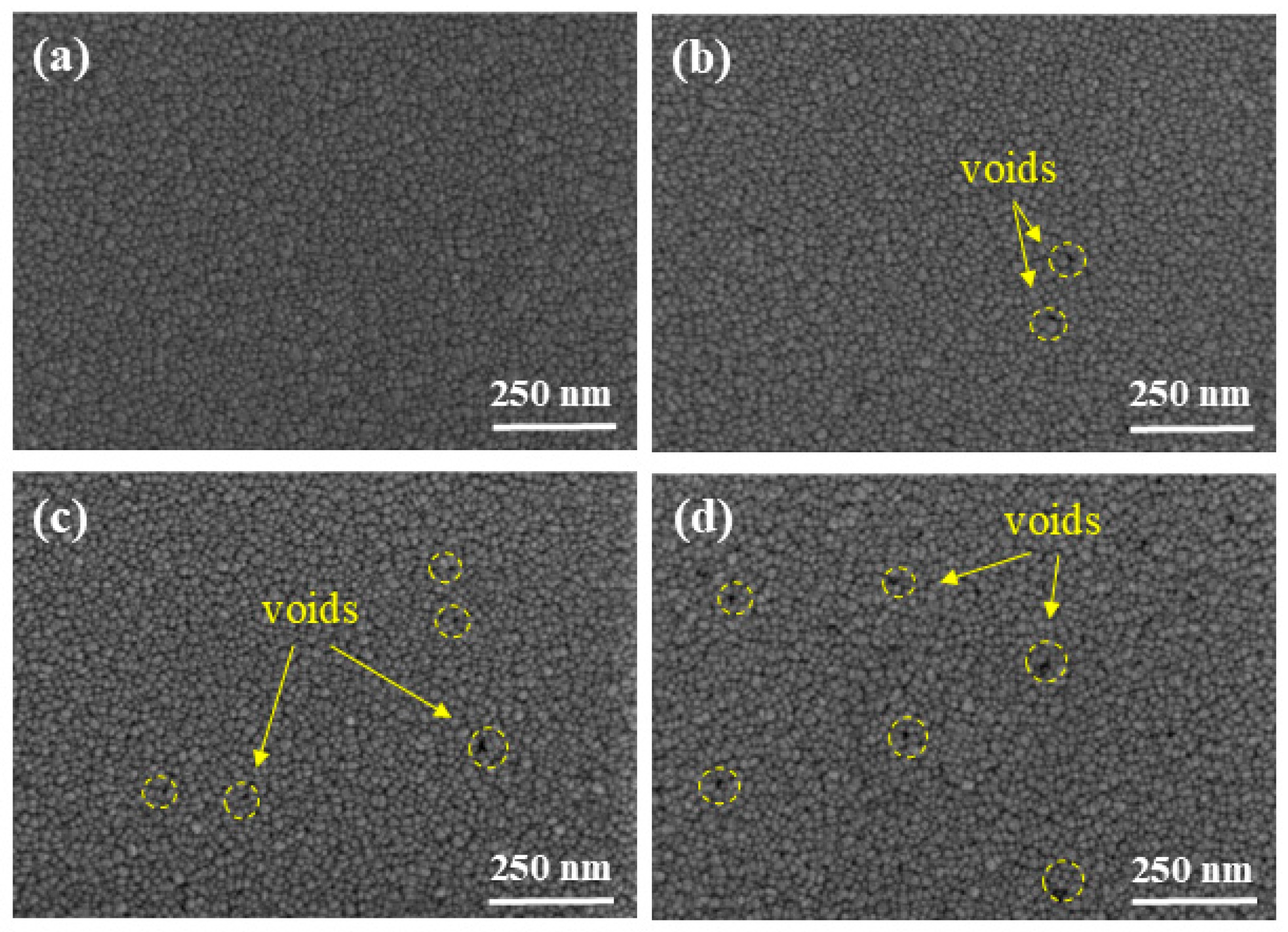
Figure 7 presents the surface SEM morphology of Cu films deposited at identical thicknesses under various gas flow rates (Samples 9#, 10#, 13# and 14#). To eliminate the influence of thickness variations on film morphology, the thickness of all Cu films was standardized by adjusting deposition time. At a lower gas flow rate of 300 mL/min, the Cu films exhibited a dense particulate structure. When the gas flow rate was increased to 600 mL/min and 900 mL/min, the films retained a particulate morphology, but the increased surface porosity was observed. This phenomenon is attributed to the following reasons: under lower working pressure conditions, the extended mean free path of gas molecules resulted in higher kinetic energy of deposited particles and enhanced surface migration, promoting denser microstructures. Conversely, at elevated flow rates (600–900 mL/min), the increased frequency of interparticle collisions shortened the mean free path and then reduced the energy of Cu particles arriving at the substrate, thereby limiting surface mobility and decreasing film density.
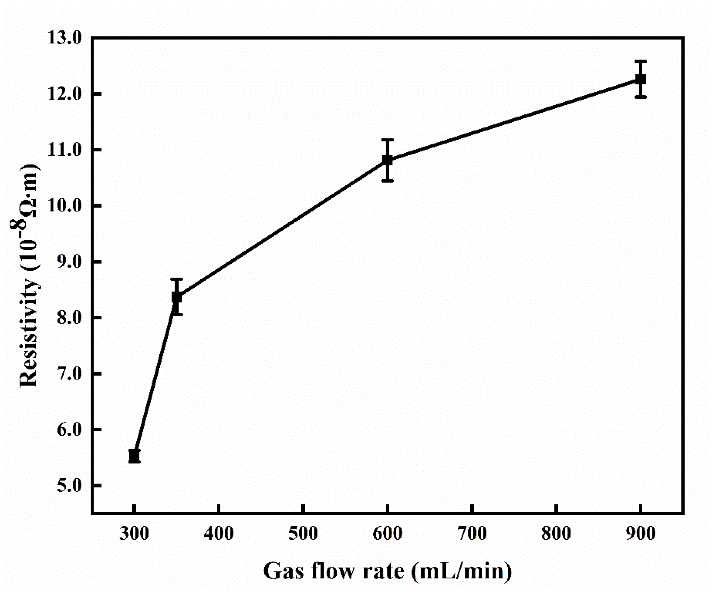
Figure 8 depicts the resistivity variations in Cu films deposited at different gas flow rates (Samples 9#–12#). The resistivity exhibited a progressive increase with elevated gas flow rates. At a gas flow rate of 300 mL/min (sample 9#), high energetic Cu atoms or clusters promoted dense microstructure (as shown in Figure 7a), yielding minimal resistivity. When the gas flow rate was increased to 350 mL/min (sample 10#), the enhanced interparticle collisions restricted surface mobility despite greater film thickness. This resulted in elevated defect density (as shown in Figure 7b), consequently increasing resistivity. Further increasing the gas flow rate to 600 mL/min and 900 mL/min (samples 13# and 14#) also increased the defect densities, as shown in Figure 7c,d, which intensified electron scattering, causing continued elevation of resistivity. By comparing between samples 11# and 13#, as well as 12# and 14#, which were deposited under identical process conditions, it is found that samples 11# and 12# exhibited lower thicknesses, which consequently led to a further increase in film resistivity. Therefore, high deposition pressure adversely affected the formation of dense, highly conductive Cu films.
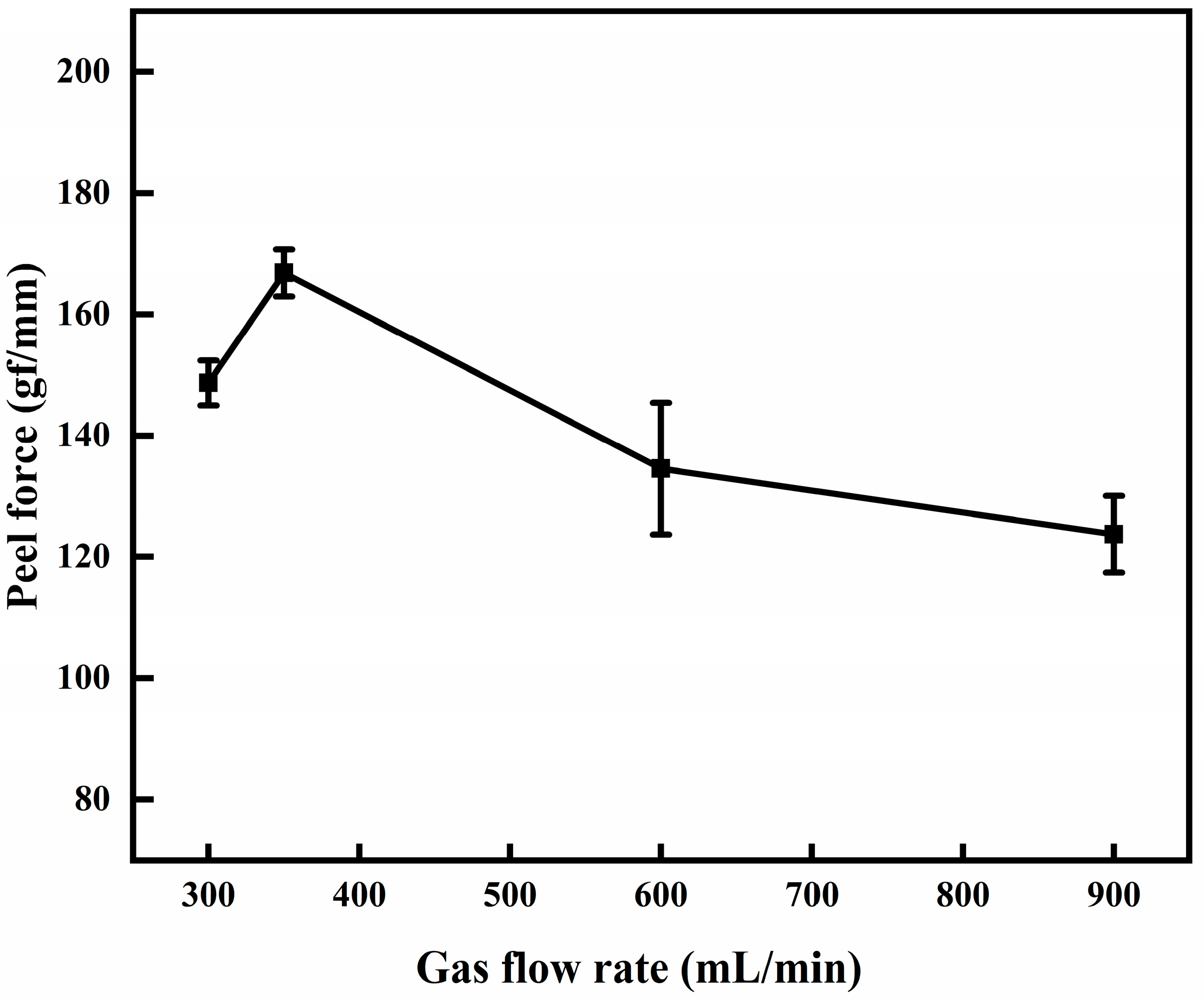
Figure 9 shows the adhesion results of Cu films prepared at different gas flow rates (Samples 9#, 10#, 13# and 14#). The adhesion strength initially increased with increasing gas flow rate, reaching a maximum at 350 mL/min before subsequently decreasing.
At the gas flow rate of 300 mL/min, high-energy Cu particles bombarded the PET substrate surface. Given the low melting point of PET (approximately 250 °C [28]), these energetic Cu particles induced the localized thermal damage to the substrate, consequently weakening interfacial bonding. When the flow rate was increased to 350 mL/min, deposited Cu species with moderated energy enabled effective embedding into PET’s microscopic asperities without inducing significant thermal degradation. This enabled synergistic interfacial reinforcement through a combination of mechanical interlocking interaction and van der Waals interactions [29], thereby maximizing adhesion strength. At further elevated flow rates (600–900 mL/min), the reduced mean free path of gas molecules decreased the energy of sputtered Cu species, resulting in suppressed surface diffusion. Consequently, Cu-PET interfacial interlocking was weakened, leading to diminished adhesion strength. These observations align with working pressure effects reported by Wang et al. [30]. Based on the above research results, a gas flow rate of 350 mL/min was established as the optimal parameter for subsequent experiments.

3.3. Effect of Substrate Temperature

Figure 10 displays the SEM surface morphology of Cu films fabricated at different substrate temperatures (Samples 10#, 15#–16#). The results showed that the substrate temperature had little influence on the surface morphology of Cu films. A dense granular microstructure was confirmed in all tested films, and negligible differences were observed in grain size. In addition, film thickness was found to be independent of deposition temperature. The deposition rate is predominantly determined by the flux of sputtered species reaching the substrate in the process of deposition, which can be expressed as Equation (5):
R = J S ρ
where R denotes the deposition rate, J represents the atomic flux reaching the substrate, S is the sticking coefficient of adatoms, and ρ means the film density. Based on the Langmuir adsorption mode [31], at low substrate temperatures, adatoms exhibit prolonged residence times, resulting in negligible desorption rates. Consequently, S remains approximately constant. Hence, the deposition rate is governed exclusively by the atomic flux (J) and is temperature-independent.
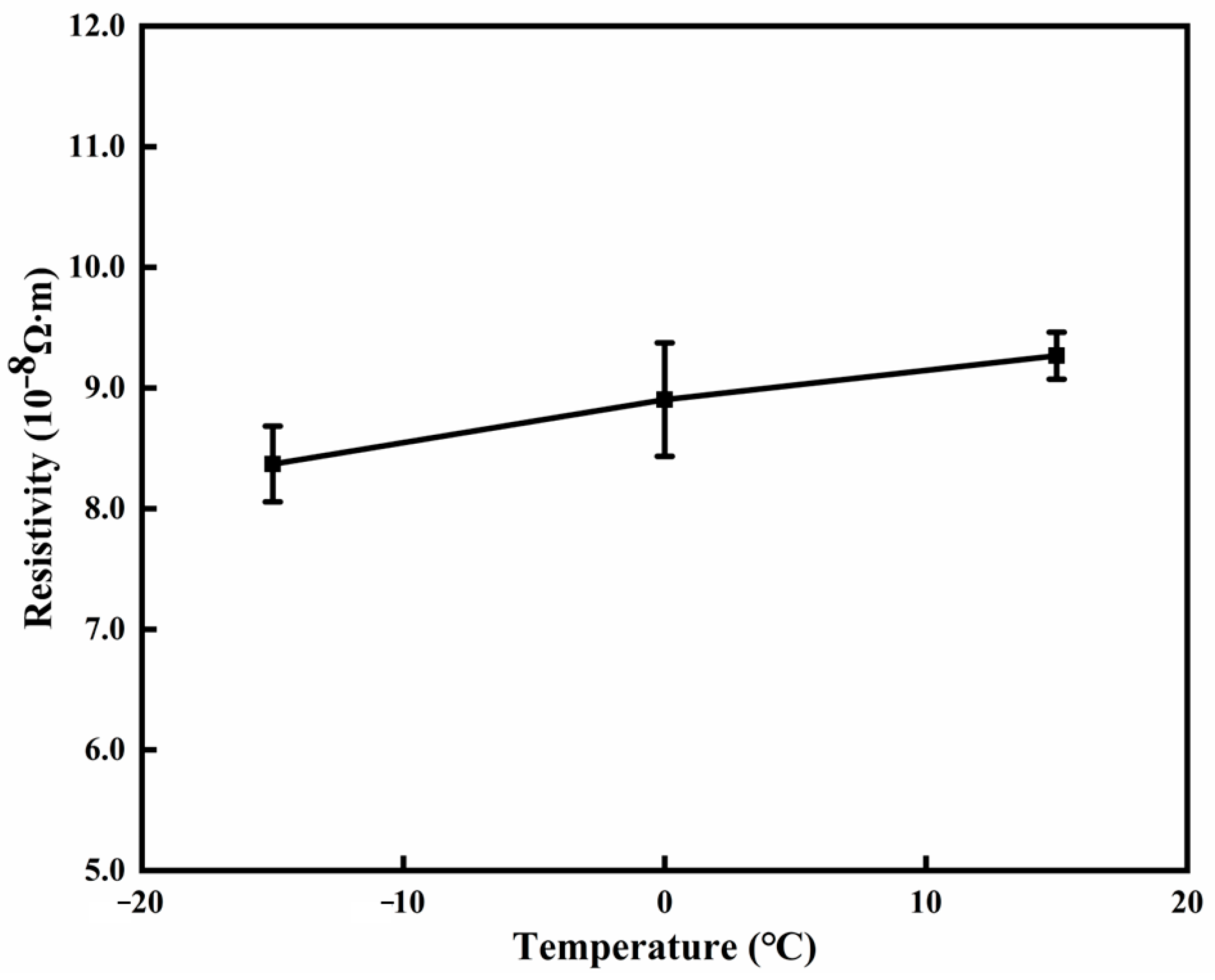
The resistivity variations in Cu films deposited at different substrate temperatures were plotted in Figure 11 (Samples 10#, 15# and 16#). No significant influence of substrate temperature on film resistivity was observed within the range of −15 °C to 15 °C. As confirmed by Figure 10 and Table 1, both film thickness and microstructure remained essentially unchanged; consequently, resistivity variations were negligible.
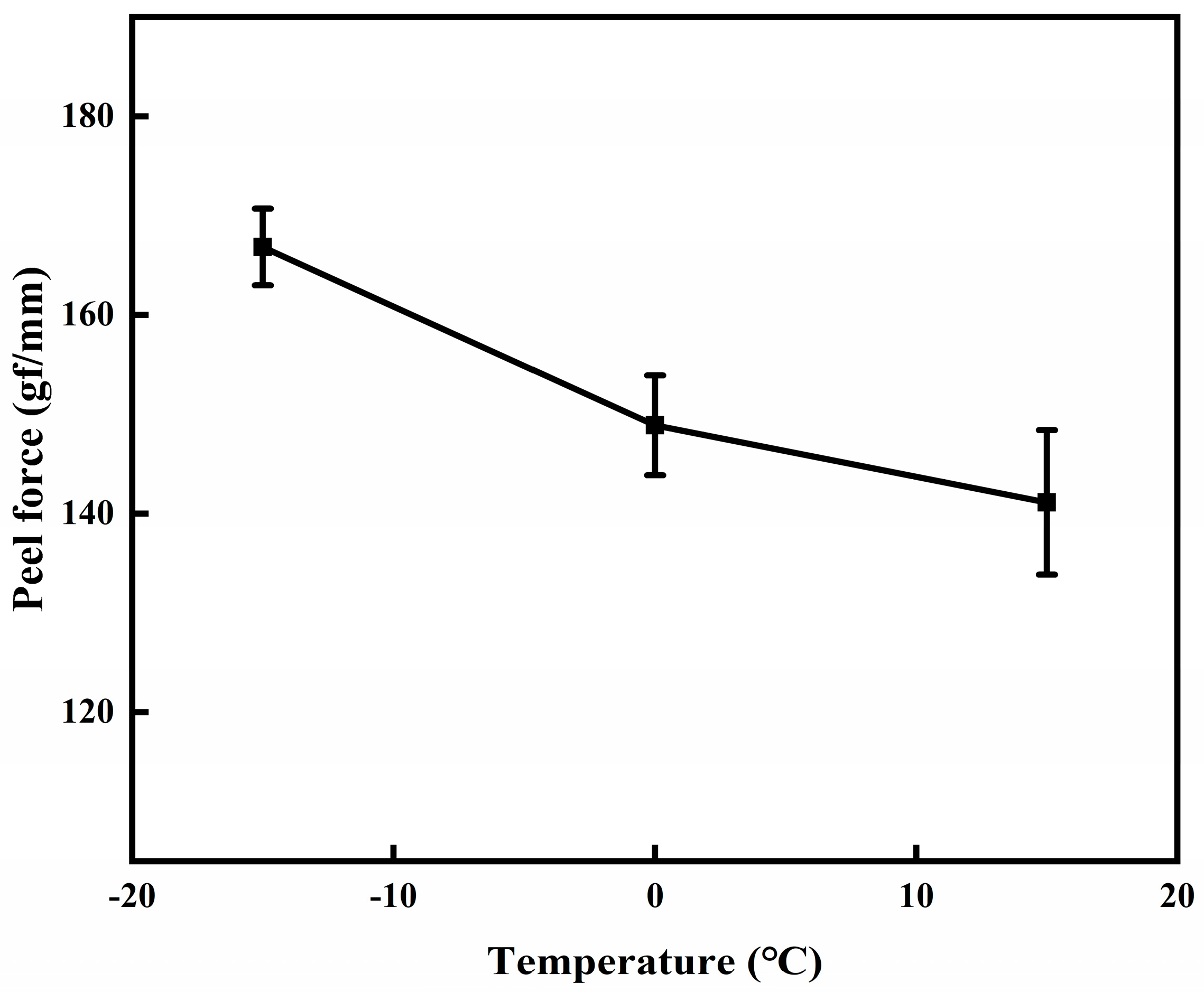
The adhesion results of Cu films deposited at various substrate temperatures are presented in Figure 12 (Samples 10#, 15#–16#). A progressive decline in adhesion strength was observed as the substrate temperature increased from −15 °C to 15 °C, attributed to the localized thermal damage at elevated temperatures. Based on the adhesion consideration, −15 °C was established as the optimal substrate temperature.

4. Conclusions

This paper systematically studied the effects of the magnetron sputtering deposition parameters, including sputtering power, gas flow rate, and substrate temperature, on the microstructure, electrical properties, and adhesion strength of Cu films fabricated on PET substrates. The conclusions are as follows:
As sputtering power increased, the deposition rate and grain size of Cu films exhibited gradual increases, while resistivity decreased. Peel tests indicated enhanced adhesion strength with increasing target power, reaching an optimum at 3.0 kW. Considering the combined requirements for low resistivity and high adhesion strength, 3 kW was identified as the optimal power parameter.
The deposition rate initially increased but declined subsequently with increasing gas flow rate, while resistivity exhibited a monotonic increase. SEM analysis confirmed progressive reduction in surface density of Cu films at elevated gas flow rates. When the gas flow rate exceeded 600 mL/min, micropores formed on the film surface, resulting in increased resistivity. Peel test results revealed a non-monotonic dependence of adhesion strength on gas flow rate, with maximum strength achieved at 350 mL/min. Therefore, based on comprehensive consideration of deposition rate, resistivity, and adhesion results, the optimal gas flow rate was determined as 350 mL/min.
Variations in substrate temperature (−15 to 15 °C) exhibited negligible effects on the microstructure and resistivity of Cu films. SEM characterization confirmed that all of the Cu films maintained dense granular structures without significant changes in grain size or thickness. However, adhesion strength demonstrated a progressive decline with increasing substrate temperature. Therefore, optimum substrate temperature was established at −15 °C based on adhesion performance evaluation.
In summary, the optimized deposition parameters for Cu films on PET substrates were established as follows: sputtering power: 3 kW; gas flow rate: 350 mL/min; substrate temperature: −15 °C; deposition time: 2 min. Under these conditions, the resulting Cu films exhibited a dense microstructure, low resistivity (8.37 × 10⁻⁸ Ω·m), and high adhesion strength (166 gf/mm), with film thickness reaching approximately 80 nm. This parameter set demonstrates a robust approach for fabricating high-performance Cu films on polymer substrates.

Author Contributions

Conceptualization, Y.Y.; writing—original draft preparation, X.H. and L.Z.; writing—review and editing, J.D.; editing and resources, L.G.; supervision, J.Z. All authors have read and agreed to the published version of the manuscript.

Funding

This work was supported by Yangtze River Delta Innovation Consortium Proof-of-Concept Program [grant number RH2500001192].

Institutional Review Board Statement

Not applicable.

Informed Consent Statement

Not applicable.

Data Availability Statement

Data is contained within the article.

Conflicts of Interest

The authors declare no conflicts of interest.

References

  1. Dun, X.; Wang, M.; Shi, H.; Xie, J.; Wei, M.; Dai, L.; Jiao, S. Composite copper foil current collectors with sandwich structure for high-energy density and safe lithium-ion batteries. Energy Storage Mater. 2025, 74, 103936. [Google Scholar] [CrossRef]
  2. Hur, J.; Lee, J.; Kim, B.Y.; Yoo, M.J.; Seo, J.H. Formation of a robust cu adhesive layer on poly (ether ether ketone) via self UV-initiated surface polymerization. J. Ind. Eng. Chem. 2022, 112, 307–315. [Google Scholar] [CrossRef]
  3. Ye, Y.S.; Huang, W.X.; Xu, R.; Xiao, X.; Zhang, W.; Chen, H.; Wan, J.; Liu, F.; Lee, H.K.; Xu, J.; et al. Cold-starting all-solid-state batteries from room temperature by thermally modulated current collector in sub-minute. Adv. Mater. 2022, 34, 2202848. [Google Scholar] [CrossRef]
  4. Wang, E.; Wang, S.; Wang, F.; Zhang, G.; Shang, L. Adhesion improvement of sputtered Cu films on flexible polymer substrates through the design of metal interlayers. Phys. Scr. 2024, 99, 075926. [Google Scholar] [CrossRef]
  5. Zaporojtchenko, V.; Strunskus, T.; Behnke, K.; Bechtolsheim, C.v.; Thran, A.; Faupel, F. Formation of metal-polymer interfaces by metal evaporation: Influence of deposition parameters and defects. Microelectron. Eng. 2000, 50, 465–471. [Google Scholar] [CrossRef]
  6. Chen, J.J.; An, Q.; Rodriguez, R.D.; Sheremet, E.; Wang, Y.; Sowade, E.; Baumann, R.R.; Feng, Z.Z. Surface modification with special morphology for the metallization of polyimide film. Appl. Surf. Sci. 2019, 487, 503–509. [Google Scholar] [CrossRef]
  7. Niu, J.; Huang, X.; Yang, H.; Li, D.; Gao, X.; Yang, L.; Chen, Q.; Sun, A.; Zheng, K.; Wang, T.; et al. Copper Polypropylene Metal Plastic Composite Copper Foil: Future Proof Anode Current Collector Solution for Lithium-Ion Batteries with High Energy Density. ACS Appl. Mater. Interfaces 2024, 16, 57603–57613. [Google Scholar] [CrossRef]
  8. Huang, J.; Tian, C.; Wang, J.; Liu, J.; Li, Y.; Liu, Y.; Chen, Z. Fabrication of selective electroless copper plating on PET sheet: Effect of PET surface structure on resolution and adhesion of copper coating. Appl. Surf. Sci. 2018, 458, 734–742. [Google Scholar] [CrossRef]
  9. Hu, J.; Zhu, D.; Wang, F.; Long, Y.; Kang, Z.; Gui, Z. Super-high interface adhesion through silver/polyimide heterojunction. Mater. Des. 2023, 233, 112276. [Google Scholar] [CrossRef]
  10. Wang, C.; Li, X.; Zhang, G. 2024 Copper Composite Current Collector Preparation Method and Application Thereof. CN115094384B, 28 July 2023. (In Chinese). [Google Scholar]
  11. Ma, Y.; Li, L.; Qian, J.; Qu, W.; Luo, R.; Wu, F.; Chen, R. Materials and structure engineering by magnetron sputtering for advanced lithium batteries. Energy Storage Mater. 2021, 39, 203–224. [Google Scholar] [CrossRef]
  12. Thornton, J.A. Influence of Apparatus Geometry and Deposition Conditions on the Structure and Topography of Thick Sputtered Coatings. J. Vac. Sci. Technol. 1974, 11, 666–670. [Google Scholar] [CrossRef]
  13. Thornton, J.A. Influence of Substrate Temperature and Deposition Rate on Structure of Thick Sputtered Cu Coatings. J. Vac. Sci. Technol. 1975, 12, 830–835. [Google Scholar] [CrossRef]
  14. Zhang, L.; Hao, X.; Wang, Y.; Yang, Y.; Gu, H.; Chu, S.; Wu, J.; Zheng, J. Microstructure and Performance Regulation of Cu Seed Layer by Magnetron Sputtering for Composite Current Collector Used in Lithium Battery. Surf. Technol. 2025, 54, 1–12. [Google Scholar] [CrossRef]
  15. Jin, Y.Z.; Wu, W.; Li, L.; Chen, J.; Zhang, J.; Zuo, Y.; Fu, J. Effect of sputtering power on surface topography of DC magnetron sputtered Ti thin films observed by AFM. Appl. Surf. Sci. 2008, 255, 4673–4679. [Google Scholar] [CrossRef]
  16. Ekpe, S.D.; Bezuidenhout, L.W.; Dew, S.K. Deposition rate model of magnetron sputtered particles. Thin Solid Film. 2005, 474, 330–336. [Google Scholar] [CrossRef]
  17. Chopra, K.L.; Randlett, M.R. Influence of deposition parameters on the coalescence stage of growth of metal films. J. Appl. Phys. 1968, 39, 1874–1881. [Google Scholar] [CrossRef]
  18. Hu, Y.; Qiu, L.; Dai, B.; Wei, X.; Ren, Y.; Ge, N.; Long, Z. Effects of microstructure of Cu thin films deposited by magnetron sputtering on electro-explosive performance. J. Funct. Mater. 2016, 47, 12152–12156. (In Chinese) [Google Scholar]
  19. Le, M.T.; Sohn, Y.U.; Lim, J.W.; Choi, G.S. Effect of sputtering power on the nucleation and growth of Cu films deposited by magnetron sputtering. Mater. Trans. 2010, 51, 116–120. [Google Scholar] [CrossRef]
  20. Fuchs, K. The conductivity of thin metallic films according to the electron theory of metals. Math. Proc. Camb. Philos. Soc. 2008, 34, 100–108. [Google Scholar] [CrossRef]
  21. Sondheimer, E.H. The mean free path of electrons in metals. Adv. Phys. 2001, 50, 499–537. [Google Scholar] [CrossRef]
  22. Zhang, G.; Li, M.; Wu, X.; Li, C.; Luo, X. Research Progress on Effect of Length Scale on Electrical Resistivity of Metals. Chin. J. Mater. Res. 2014, 28, 81–87. (In Chinese) [Google Scholar] [CrossRef]
  23. Wang, M.; Zhang, B.; Zhang, G.P.; Yu, Q.Y. Effects of interface and grain boundary on the electrical resistivity of Cu/Ta multilayers. J. Mater. Sci. Technol. 2009, 25, 699–702. [Google Scholar] [CrossRef]
  24. Mayadas, A.F.; Shatzkes, M. Electrical-resistivity model for polycrystalline films: The case of arbitrary reflection at external surfaces. Phys. Rev. B 1970, 1, 1382–1389. [Google Scholar] [CrossRef]
  25. Doerner, M.F.; Nix, W.D. Stresses and deformation processes in thin films on substrates. Crit. Rev. Solid State Mater. Sci. 1988, 14, 225–268. [Google Scholar] [CrossRef]
  26. Jiang, P. Effect of deposition pressure on structural and optical properties of ZnO films. Master’s Thesis, Soochow University, Suzhou, China, May 2009. [Google Scholar]
  27. Kusano, E. Structure-Zone Modeling of Sputter-Deposited Thin Films: A Brief Review. Appl. Sci. Converg. Technol. 2019, 28, 179–185. [Google Scholar] [CrossRef]
  28. Threepopnatkul, P.; Thinsoongnoen, P.; Misut, P.; Autama, S.; Kulsetthanchalee, C. Preparation and characterization of PET/SEBS incorporated with organomontmorillonite. IOP Conf. Ser. Mater. Sci. Eng. 2020, 965, 012019. [Google Scholar] [CrossRef]
  29. Aradhya, S.; Frei, M.; Hybertsen, M.; Venkataraman, L. Van der Waals interactions at metal/organic interfaces at the single-molecule level. Nat. Mater. 2012, 11, 872–876. [Google Scholar] [CrossRef]
  30. Wang, L.; Zhang, K.; Wang, H.; Wang, Y.; Xiong, Y.; Wu, C.; Li, K.; Zhou, H. Recent Research Progress of Generation Mechanism and Influence Factors of Intrinsic Stress in Vacuum Deposited Copper Films. Vac. Cryog. 2021, 27, 103–114. (In Chinese) [Google Scholar] [CrossRef]
  31. Langmuir, I. The adsorption of gases on plane surfaces of glass, mica and platinum. J. Am. Chem. Soc. 1918, 40, 1361–1403. [Google Scholar] [CrossRef]
Figure 1. Effect of sputtering power on the deposition rate of Cu films.
Coatings 15 01089 g001
Figure 2. Surface morphology of Cu films prepared at different sputtering powers: (a) 1 kW (6#, 80 nm); (b) 1.5 kW (7#, 85 nm); (c) 2 kW (3#, 91 nm); (d) 2.5 kW (8#, 79 nm); (e) 3 kW (9#, 77.2 nm).
Coatings 15 01089 g002
Figure 3. AFM topography of Cu films fabricated at different target powers (1 µm × 1 µm): (a) 1 kW (6#, RMS: 0.85 nm); (b) 3 kW (9#, RMS: 0.86 nm).
Coatings 15 01089 g003
Figure 4. The resistivity of Cu films prepared at different sputtering powers.
Coatings 15 01089 g004
Figure 5. Peel force of Cu films prepared at different sputtering powers.
Coatings 15 01089 g005
Figure 6. Effect of gas flow rate on film thickness and deposition rate.
Coatings 15 01089 g006
Figure 7. Surface morphology of Cu films prepared at different gas flow rates: (a) 300 mL/min (9#, 77.2 nm); (b) 350 mL/min (10#, 80.8 nm); (c) 600 mL/min (13#, 80.5 nm); (d) 900 mL/min (14#, 80.1 nm).
Coatings 15 01089 g007
Figure 8. Resistivity of Cu films deposited at various gas flow rates.
Coatings 15 01089 g008
Figure 9. Peel force of Cu films prepared at various gas flow rates.
Coatings 15 01089 g009
Figure 10. Surface morphology of Cu films deposited at different substrate temperatures: (a) −15 °C (10#, 80.8 nm); (b) 0 °C (15#, 79 nm); (c) 15 °C (16#, 82 nm).
Coatings 15 01089 g010
Figure 11. Resistivity of Cu films deposited at various substrate temperatures.
Coatings 15 01089 g011
Figure 12. Peel force of Cu films fabricated at various substrate temperatures.
Coatings 15 01089 g012
Table 1. Deposition parameters of Cu films.
Number Target Power
/kW
Gas Flow Rate
/(mL·min−1)
Working Pressure
/Pa
Deposition
time/min
Temperature of Cooling Roll
/℃
Thickness
/nm
Series 1: Different target power with identical deposition times
1# 1 300 0.1 3 −15 40.8
2# 1.5 61.4
3# 2 91
4# 2.5 102
5# 3 115
Series 2: Different target power with nearly identical film thickness
6# 1 300 0.1 6 −15 80
7# 1.5 4 85
3# 2 3 91
8# 2.5 2.5 79
9# 3 2 77.2
Series 3: Different gas flow rates with identical deposition times
9# 3 300 0.1 2 −15 77.2
10# 350 0.2 80.8
11# 600 0.3 67.1
12# 900 0.4 63.6
Series 4: Different gas flow rates with nearly identical film thickness
9# 3 300 0.1 2 −15 77.2
10# 350 0.2 80.8
13# 600 0.3 3 80.5
14# 900 0.4 80.1
Series 5: Different substrate temperature with identical deposition times
10# 3 350 0.2 2 −15 80.8
15# 0 79
1 6# 15 82
Disclaimer/Publisher’s Note: The statements, opinions and data contained in all publications are solely those of the individual author(s) and contributor(s) and not of MDPI and/or the editor(s). MDPI and/or the editor(s) disclaim responsibility for any injury to people or property resulting from any ideas, methods, instructions or products referred to in the content.