Abstract
Chemical vapor deposition (CVD) is a crucial technique for fabricating high-performance amorphous silicon coatings, leveraging its process flexibility and microstructural controllability. Optimizing processes like hot-wire chemical vapor deposition, plasma-enhanced chemical vapor deposition, and catalytic chemical vapor deposition enable precise regulation of coating density, surface roughness, and chemical bonding. These amorphous silicon coatings exhibit outstanding tribological properties and exceptional corrosion resistance, primarily attributed to their unique amorphous structure eliminating grain boundary defects and forming dense passivation films. Future research should focus on intelligent process development, multi-field coupling failure analysis, environmental friendliness enhancement, and lifespan prediction models to advance this technology.
1. Introduction
The rapid development of modern industrial technology has imposed higher requirements on coating materials serving in extreme environments, particularly in critical fields such as aerospace nuclear energy equipment and deep-sea exploration devices. Coating materials must not only exhibit excellent mechanical properties and corrosion resistance but also maintain stable tribological performance and long-term service life under complex working conditions [1,2,3,4]. As an atomic-level precision-controlled thin-film fabrication technology, CVD enables the construction of uniform and dense amorphous silicon-based coatings on complex geometric surfaces through directional transport of gaseous precursors and regulation of surface reaction kinetics. Its process flexibility and microstructural controllability provide a vital technical pathway for developing new-generation high-performance protective coatings [5,6]. In recent years, breakthroughs in novel CVD technologies such as plasma-assisted and laser-activated systems have facilitated successful applications in cutting-edge fields including flexible electronic packaging, nuclear reactor cladding protection, and microelectromechanical systems (MEMSs). These advancements demonstrate interfacial bonding strength and three-dimensional structural conformality that traditional coating technologies cannot achieve [7,8,9,10].
Amorphous silicon-based materials demonstrate revolutionary advantages in surface engineering due to their unique short-range ordered and long-range disordered structure, effectively eliminating failure-sensitive features of traditional crystalline materials such as grain boundaries and dislocations [11,12]. Compared to physical vapor deposition techniques like magnetron sputtering and arc ion plating, CVD exhibits three core advantages in fabricating amorphous silicon coatings:
- Atomic-level doping: Precursor molecular design enables atomic-level incorporation of Si-C-N-O multi-component systems.
- Nanoscale structural control: Synergistic regulation of flow–temperature fields within reaction chambers allows precise construction of gradient composite structures at the nanoscale.
- Low-temperature processing: Plasma excitation technology reduces deposition temperatures below 200 °C, significantly expanding applications for thermally sensitive substrates like polymers [13,14].
These technological features have enabled breakthrough applications of CVD-fabricated amorphous silicon coatings in high-end fields, including semiconductor passivation layers (thickness uniformity ± 2%) and precision mold anti-adhesion coatings (friction coefficient < 0.1). Notably, the global carbon neutrality initiative has driven green and low-carbon CVD process innovation to the forefront of current research. Emerging strategies such as novel precursor design, plasma pulse modulation technology, and AI-assisted process optimization methods are accelerating the development of environmentally friendly amorphous silicon coating preparation technologies [15,16]. This technological evolution not only aligns with sustainable development principles but also pioneers innovative applications in emerging fields like new energy systems and biomedical devices. This paper systematically reviews the latest research advancements in CVD technology for the preparation of amorphous silicon-based coatings, with an in-depth focus on two core dimensions: interfacial tribological behavior mechanisms and corrosion protection characteristics. By comprehensively analyzing the structure–property relationships between the microstructural features and macroscopic performance of the coatings, we elucidate the wear-inhibition mechanisms of amorphous silicon coatings and the evolution patterns of passivation films in complex media environments. These findings provide a theoretical foundation for expanding their industrial applications in surface engineering.
While recent reviews have comprehensively covered aspects of CVD processing techniques [9,15,17,18,19] or the general applications of amorphous silicon-based coatings [20,21,22,23], a focused analysis bridging the critical structure–property–performance relationships specifically governing their tribological and corrosion protection mechanisms remains less explored. This paper systematically reviews the latest advancements in CVD-fabricated amorphous silicon-based coatings, with a dedicated focus on elucidating the fundamental mechanisms underpinning their interfacial tribological behavior and corrosion resistance—two paramount properties determining longevity in harsh environments. This study conducts an integrated analysis to elucidate how tailored CVD processes influence the microstructure of the coatings and further investigates how these microstructural features determine the macroscopic tribological performance and corrosion protection efficacy of the coatings. By synthesizing and critically analyzing the structure–property–performance relationships across diverse amorphous silicon material systems, we aim to clarify the wear-inhibition mechanisms during sliding contact and the evolution dynamics of protective passivation films in aggressive media.
2. Chemical Vapor Deposition for the Preparation of Amorphous Silicon Coatings
CVD is a process in which volatile precursors are introduced into the reaction zone to undergo chemical reactions. The byproducts are transported away from the deposition region, while non-volatile materials form and diffuse to grow on the substrate surface [24,25]. As illustrated in Figure 1, the basic CVD process involves gaseous precursor molecules entering the reaction chamber, where gas-phase chemical reactions generate reactive species. These reactive species are delivered to the substrate surface, undergo surface chemical reactions, and deposit as solid coatings. The byproducts desorb from the substrate surface and are expelled, ultimately achieving efficient coating deposition.
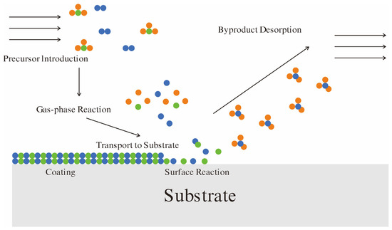
Figure 1.
Basic process of CVD. The different colored rounds represent different types of atoms. Gas molecules are composed of several atoms of the same color (i.e., the same type of atom) or different colors (i.e., different types of atoms).
2.1. Material Systems for Chemical Vapor Deposition (CVD) of Amorphous Silicon
Amorphous silicon-based coating systems fabricated via CVD exhibit diversified development characteristics, primarily including three major categories: hydrogenated amorphous silicon (a-Si:H), silicon carbide (a-SiC), and silicon carbonitride (a-SiCN). By regulating precursor compositions and deposition energy fields, hydrogenated systems achieve effective passivation of dangling bond defects under low-temperature conditions, carbon-doped systems construct high-strength tetrahedral network structures, and nitrogen-co-doped systems form three-dimensional covalent topological configurations.
Table 1 reveals distinct CVD method preferences across amorphous silicon material systems. a-SiCN coatings consistently employ RP-CVD and PE-CVD, while a-SiC exclusively uses PE-CVD. In contrast, a-Si:H demonstrates broad compatibility with multiple techniques. The specialized a-SiOC:H system solely utilizes RP-CVD. This material-specific technique distribution highlights fundamental differences in synthesis requirements across amorphous silicon variants, with a-Si:H exhibiting exceptional methodological versatility.

Table 1.
Typical CVD processing techniques for amorphous silicon films.
2.2. Energy-Field Modulated CVD: HWCVD, PECVD, and CCVD
2.2.1. Hot-Wire Chemical Vapor Deposition
HWCVD, alternatively termed catalytic CVD or filament-assisted CVD, employs thermally activated filaments to induce pyrolytic dissociation of precursor gases. This configuration maintains a thermal gradient where the substrate temperature remains below the filament operating range, facilitating surface reactions of precursor decomposition products to deposit coating layers. Meng and Wu et al. [39] employed HWCVD to prepare intrinsic hydrogenated amorphous silicon (i-a-Si:H) coatings by introducing pure silane to grow a buffer layer at a filament temperature of 1650 °C, followed by sequential deposition of bilayer-structured main layers at 1800 °C and 1900 °C. The resulting amorphous silicon coatings exhibited high density, low defect concentration, optimized hydrogen content, and refined microstructure. Tarazona and Khokhar et al. [40] utilized an HWCVD system with 15 parallel tungsten filaments, adjusting substrate temperature by varying filament diameters to influence deposition. The a-Si:H coatings were deposited at 0.01 mbar using a silane–hydrogen gas mixture (2.4:1 ratio), with filament temperature maintained at 1850 °C to ensure complete dissociation of SiH4. Wang and Shen et al. [41] developed a customized HWCVD setup to deposit amorphous silica (a-SiO2) coatings on graphite substrates, achieving an average thickness of 1.2 μm and a growth rate of 0.3 μm/h.
These empirical optimizations collectively validate the fundamental interplay between filament temperature and substrate thermal gradient in governing coating properties. The hydrogen content, defect density, and intrinsic stress of a-Si:H films are critically governed by the synergistic interplay between filament temperature (Tf) and the thermal gradient relative to the substrate (Ts). Elevated Tf efficiently cracks SiH4, increasing the flux of reactive hydrogen and silicon radicals to the growth surface. This promotes Si-H bond formation and higher total hydrogen incorporation. Conversely, higher Ts or a steeper Tf–Ts gradient enhances surface mobility of adsorbed species, facilitating the dissociation of weak poly-hydride bonds, H2 desorption, and network reconstruction toward stable monohydride (Si-H) configurations—thereby reducing total hydrogen content while optimizing bonding quality. Defect density (primarily dangling bonds) is minimized through complementary mechanisms: high Tf suppresses defect-prone higher silanes and enables robust Si-Si/Si-H bonding, while an optimal Ts gradient ensures sufficient adatom mobility for denser tetrahedral coordination and timely H passivation of nascent defects. Notably, excessively low Ts yields porous, poorly passivated networks, whereas excessively high Ts accelerates H desorption and dangling bond re-exposure. Intrinsic stress (typically compressive) emerges from competing factors: high Tf induces tensile thermal stress via radiative heating yet generates compressive “atomic peening” stress through high-energy particle bombardment; large Tf–Ts gradients favor lower/neutral stress by “freezing” atoms into porous microstructures on cold substrates; and moderate Ts elevation mitigates excessive compression by enhancing atomic relaxation. Consequently, the optimization of a-Si:H properties require precise balancing of Tf-driven precursor activation and Ts-mediated surface kinetics within a defined thermal window.
2.2.2. Plasma-Enhanced Chemical Vapor Deposition
PECVD is a technique that utilizes plasma activation of precursor gases for deposition. Unlike HWCVD, PECVD employs plasma energy to decompose precursors, enabling deposition at lower temperatures.
Key process parameters for PECVD technology have evolved continuously under the demands of new materials, device miniaturization, and advanced manufacturing processes. Xu and Tang et al. [42] achieved room-temperature deposition of low-hydrogen-content a-SiNx/a-SiNxOy thin films using argon-diluted silane and pure nitrogen as reaction gases. Jafari and Linke et al. [43] prepared amorphous films on single-crystal silicon substrates using PECVD technology. They found that in dense amorphous films deposited at high substrate temperatures (Ts > 200 °C), hydrogen atoms tend to migrate into the interface bubbles and form hydrogen molecules (H2). This process results in a continuous buildup of pressure inside the bubbles. Upon exceeding a critical internal pressure threshold, micro-explosions initiate within the bubbles. This phenomenon triggers interfacial delamination, corresponding to characteristic sharp peaks (SPs) in hydrogen effusion spectra, as illustrated in Figure 2. Lukianov and Klyui et al. [44] engineered amorphous films by strategically modulating RF discharge power and silane flow rates. This parametric optimization yielded coatings with tunable hardness (8.6–14.8 GPa) and exceptional wear resistance. Lin and Feng et al. [45] fabricated a-Si:H layers on p-type multicrystalline black silicon substrates at 200 °C. Their analysis demonstrated that active hydrogen species within the deposited films simultaneously passivate surface defect states and bulk trap states in the underlying p-mc-b-Si. Li and Jiang et al. [46] synthesized a-SiCx:H films embedded with carbon nanostructures via PECVD. They studied how substrate temperature affected the structure and growth of these nanostructures. The film is a multiphase material, with spherical graphite-like nanostructures embedded in an amorphous matrix. As the substrate temperature rose, the nanostructures grew by merging with nearby structures. At 300 °C, ultrafine graphite units appeared, showing that higher temperatures enhanced graphitization, as illustrated in Figure 3.
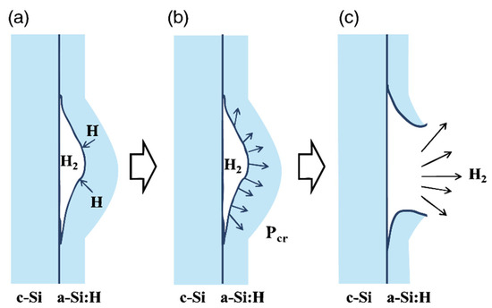
Figure 2.
Subsurface bubble rupture-mediated film delamination mechanism (Ts > 200 °C). (a) Desorption of atomic hydrogen from bubble surface and formation of H2 molecules; (b) Increase of pressure inside the bubble to the critical point; (c) Film delamination due to abrupt hydrogen release (explosion) [43].
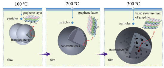
Figure 3.
Formation mechanism of carbon nanostructures [47].
Table 2 summarizes the critical process parameters for preparing amorphous coatings via PECVD. PECVD enables precise control over amorphous silicon-based coatings through synergistic modulation of four core parameters: plasma power (RF), reactive gas composition, Ts, and deposition pressure. The RF power governs plasma density and ion bombardment energy: higher power enhances precursor dissociation and promotes cross-linking of Si-C/Si-N bonds, thereby increasing hardness. However, excessive power risks hydrogen effusion and interfacial delamination due to subsurface H2 bubble formation, particularly at Ts > 200 °C. Gas composition directly dictates stoichiometry and bonding states: elevating the N/Si ratio maximizes Si-N bonding for superior wear resistance, reducing friction coefficients by >90%. Substrate temperature critically balances structural relaxation against hydrogen stability: higher Ts facilitates Si-OH → Si-O-Si conversion and densification, lowering friction to 0.15, yet exceeding 400 °C accelerates H desorption, re-exposing dangling bonds. Low deposition pressure (0.01–0.7 torr) extends molecular mean free paths, suppressing gas-phase nucleation to achieve uniform coatings, whereas higher pressure may induce porous polymer-like structures. Critically, parameter interdependence defines performance limits: low-temperature processes require Ar dilution and reduced power to mitigate defects, while carbon nanostructure evolution in a-SiC:H necessitates coupled control of Ts and RF power. Thus, optimizing PECVD films demands a holistic “plasma–surface–substrate” strategy, where power activates reactions, gas chemistry designs bonding networks, Ts tunes kinetic relaxation, and pressure ensures homogeneous delivery, all while avoiding deleterious couplings.
Table 2.
Key process parameters for PECVD.
PECVD enables directional control of film chemical bonding states, hydrogen content, and mechanical properties by adjusting parameters such as plasma power, reactive gas composition, deposition temperature, and pressure. This technology effectively passivates surface defects while optimizing structural densification and interfacial characteristics of coatings, making it suitable for preparing multi-component material systems. The strong correlations between process parameters and film performance indicate that plasma reaction kinetics critically determine the cross-linking degree of the amorphous network and defect density. These factors govern coating hardness, wear resistance, and environmental adaptability, thereby providing technical support for the multi-scale design of functionalized coatings.
2.2.3. Catalytic Chemical Vapor Deposition
CCVD introduces gaseous reactants into a reaction chamber, where catalysts facilitate reactant decomposition or reactions to deposit solid materials onto substrates. Compared to conventional CVD, CCVD reduces reaction temperatures or accelerates reaction kinetics through catalytic activation [61]. Utilizing a deposition temperature of 450 °C, Wang and Tu et al. [62] fabricated n-a-Si:H films on silicon carbide-coated textured glass substrates, demonstrating robust film–substrate adhesion. Song and Hong et al. [63] implemented a tungsten filament array at 1750 °C to deliver precursor gases into the reaction chamber, integrating active substrate cooling. This configuration achieved low-temperature (200 °C) synthesis of a-Si:C films.
Compared to conventional CVD processes, CCVD technology significantly reduces substrate temperature thresholds and enhances deposition efficiency by optimizing catalyst active site distribution and reaction pathways. The catalyst (typically tungsten filaments or metal provides localized activation sites—elevated filament temperatures enable complete precursor dissociation while maintaining low substrate temperatures. This sharp thermal gradient minimizes thermal stress on sensitive substrates, such as polymers or textured glass, while ensuring sufficient surface mobility for dense film growth. Critically, CCVD’s unique “catalytically activated gas–substrate” interplay allows decoupling of precursor dissociation energy from substrate thermal budgets: filament/nanoparticle catalysts absorb high-temperature energy inputs, liberating reactive species that undergo low-barrier surface reactions on cooler substrates. This mechanism enables microstructure tailoring unattainable by thermal CVD, such as nanocrystalline/amorphous dual-phase formation via selective catalyst-mediated bonding. However, catalyst aging and spatial non-uniformity in large-scale systems remain key challenges. Future advances demand co-optimization of catalyst lifetime management, 3D thermal field design, and precursor–catalyst affinity matching to harness CCVD’s full potential for functional coatings on thermally fragile substrates.
2.3. Comparative Analysis of Deposition Techniques
2.3.1. Comparative Analysis of CVD Techniques
The fundamental differences in activation mechanisms among HWCVD, PECVD, and CCVD lead to distinct pathways for amorphous network formation, as summarized in Table 3. These differences critically determine coating density, defect concentration, and interfacial bonding strength.
Table 3.
Comparative analysis of CVD techniques for amorphous silicon coatings.
As evident from Table 3, the core differences between HWCVD, PECVD, and CCVD fundamentally stem from the distinct nature of their energy transfer pathways. HWCVD relies on radiative heating from a high-temperature filament. This induces homogeneous thermal pyrolysis in the gas phase, completely dissociating precursors into highly reactive radicals. Subsequent thermal reconstruction reactions occur on the substrate surface. This process forcibly eliminates weak bonds, promoting short-range ordering into Si-Si tetrahedra. However, the intense radiative heating poses a significant risk of damage to thermally sensitive substrates. PECVD utilizes the energy of non-equilibrium plasma. High-energy electron collisions cause electronic excitation and dissociation of precursors, generating ions and excited neutral species. While the continuous bombardment of the growth surface by the plasma (ion-assisted deposition) enhances film densification, it can simultaneously implant hydrogen cluster defects or initiate micro-void formation. In contrast, CCVD employs heterogeneous catalysis mediated by active sites on a catalyst surface. Precursors undergo adsorption–dissociation–desorption processes on the catalyst. The resulting reaction intermediates then migrate to the substrate with low activation energy for film formation. Although this “moderate activation” mechanism avoids high-energy damage, it is inherently constrained by catalyst deactivation and contamination risks.
These fundamental differences in energy transfer dictate that the amorphous network formation induced by the three technologies follows markedly distinct kinetic pathways:
In the high-thermal environment of HWCVD, thermodynamics dominates reconstruction. Silicon atoms achieve maximum coordination through surface diffusion, forming disordered networks with low hydrogen content and high cross-linking density. However, the rapid quenching process leads to the accumulation of tensile thermal stress.
The plasma nature of PECVD promotes a kinetically frozen mechanism. The high deposition rate prevents atoms from reaching their energy-minimum positions, resulting in metastable structures with mixed bonding configurations. While ion bombardment enhances film hardness, it concurrently induces bond angle distortion and residual compressive stress.
The catalytic pathway of CCVD enables surface-directed growth. Reaction intermediates assemble layer by layer on the substrate surface, forming amorphous structures with chemically graded compositions. Its low-temperature characteristic (200–500 °C) virtually eliminates thermal stress. Nevertheless, catalyst residue can disrupt network continuity.
These structural characteristic differences further manifest as three fundamental trade-offs in technological application:
Structural Integrity vs. Substrate Compatibility: While HWCVD can produce near-ideal amorphous networks, it is restricted to high-temperature-resistant substrates. PECVD sacrifices bonding uniformity to achieve compatibility with thermally sensitive materials like polymers. Although CCVD enables low-temperature, efficient deposition, catalyst longevity constricts process stability.
Defect Control vs. Energy Cost: HWCVD eliminates hydrogen defects through high-temperature annealing at the cost of megawatt-level energy consumption. PECVD suppresses gas-phase nucleation under low pressure but concurrently introduces plasma-induced bulk defects. CCVD avoids high-energy damage yet requires complex post-processing to remove catalytic impurities.
Interface Engineering Flexibility: The thermal effect in HWCVD promotes covalent bonding at the substrate–coating interface but may induce elemental interdiffusion. Plasma pretreatment in PECVD enables atomic-level interface cleaning, yet excessive bombardment can generate amorphous interlayers. CCVD allows selective deposition through catalyst patterning, but its extreme sensitivity to substrate surface cleanliness substantially increases process control complexity.
Table 2 and Table 3 systematically outline the key process parameters of different CVD techniques for fabricating amorphous silicon-based coatings, with different process parameters suitable for different material substrates. HWCVD stands out for its ability to achieve high Si–Si bond density and low hydrogen content, which is attributed to thermal reconstruction at high filament temperatures ranging from 1800 to 2000 °C, a characteristic that makes it ideal for coatings demanding exceptional structural integrity such as semiconductor passivation layers. However, it has limitations, including high thermal stress that restricts its use to high-temperature-resistant substrates like ceramics and metals, and high energy consumption at the megawatt level, with its optimal applications lying in high-precision tools, optical components, and scenarios requiring ultra-dense coatings with thickness uniformity within ±2%. PECVD offers the advantage of low-temperature deposition, typically between 50 and 300 °C, enabling compatibility with thermally sensitive substrates such as polymers and flexible electronics, and also allows precise control over stoichiometry through gas composition; however, it has drawbacks, including plasma-induced defects like hydrogen clusters and micro-voids that may compromise long-term stability, as well as being limited to moderate hardness in the range of 8.6–14.8 GPa, with its optimal applications in MEMS devices, biomedical implants, and flexible electronics where substrate temperature is a critical factor. CCVD boasts atomic-level dopant control and low intrinsic stress, striking a balance between moderate deposition rates of 0.5–2 μm/h and substrate compatibility within a temperature range of 200–500 °C. Nevertheless, it faces challenges such as catalyst contamination risks and aging that reduce process stability, and the need for complex post-processing, with its optimal applications being in functionally graded coatings like tribological layers with tunable friction coefficients.
Current technological boundaries are being transcended through energy-field synergy strategies: Plasma-assisted catalytic CVD (PAC-CVD) couples plasma excitation with catalytic dissociation, enabling high-crosslinking-density a-SiCxNy deposition within the 100–300 °C range. Pulsed hot-wire HWCVD modulates thermal radiation cycles, preserving high-temperature bonding advantages while restricting substrate temperature rise below 150 °C. Such hybrid techniques demonstrate potential to reconcile the inherent dilemma between “low-temperature deposition” and “high network integrity,” thereby advancing breakthrough applications of amorphous silicon coatings in emerging fields including flexible electronics and biosensing interfaces.
2.3.2. Comparison with Non-CVD Techniques
Amorphous silicon-based coatings can also be fabricated via non-CVD techniques, primarily including physical vapor deposition (PVD) methods and alternative processes. These techniques differ fundamentally from CVD in deposition mechanisms, leading to distinct coating properties and application scopes.
Physical vapor deposition (PVD) techniques such as magnetron sputtering and electron-beam evaporation rely on physical processes like ion bombardment and thermal evaporation to transfer material from a solid source to the substrate without chemical reactions; as a line-of-sight process, PVD limits conformal deposition on complex 3D surfaces, unlike CVD, which uses gaseous precursors and chemical reactions to enable uniform coverage of intricate geometries such as microchannels in MEMS [7,64]. Magnetron sputtering typically operates at 200–500 °C, while electron-beam evaporation may require higher temperatures to melt the target, restricting applications on thermally sensitive substrates like polymers compared to low-temperature CVD variants such as PECVD (<200 °C) [65]. In terms of coating properties, sputtered coatings can achieve high density via ion-assisted densification, but arc sputtering may introduce micro-particle inclusions that increase surface roughness [66], whereas CVD achieves lower defect concentrations (e.g., hydrogen-passivated dangling bonds in a-Si:H) through precise gas-phase control [67]; PVD relies on target composition, limiting atomic-level control over multi-component systems like Si-C-N-O, while CVD enables tailored doping via precursor design (e.g., NH3 for N-doping in a-SiCN) [68]; additionally, high-energy ion bombardment in PVD enhances adhesion but may induce residual stress, whereas CVD, especially low-temperature PECVD, achieves stable adhesion without excessive stress [69].
Beyond PVD, emerging techniques such as pulsed laser deposition (PLD), sol–gel, and carbothermal synthesis offer unique pathways for fabricating amorphous silicon-based coatings but have inherent limitations: PLD ejects material by laser ablation of the target, enabling stoichiometric transfer of complex compositions like SiCxNy, yet it often results in rough surfaces due to particulate ejection and requires annealing at temperatures above 600 °C to reduce defects, which restricts its application on thermally sensitive substrates [70]; the sol–gel method involves hydrolysis of liquid precursors to form a gel, which is then dried and annealed to produce coatings, and while it is suitable for large-area, low-cost coatings, it requires high-temperature annealing to remove organic substances, leading to porous structures with low hardness, far lower than that of CVD coatings [69]; and carbothermal synthesis converts silica and carbon precursors into SiC at high temperatures (>1500 °C), a method that can produce micron-sized spherical particles suitable for structural applications but fails to obtain ultra-thin and uniform films required for electronic devices [71].
In summary, PVD excels in high-deposition-rate scenarios, while alternative processes offer cost advantages for large-area, low-performance applications. However, CVD remains superior for high-precision requirements—such as atomic-level doping, conformal deposition, and low-temperature processing—making it irreplaceable in advanced fields like aerospace and microelectronics.
3. Tribological Properties of Amorphous Silicon Coatings
The optimization of tribological performance in amorphous silicon coatings represents a critical research direction in materials science and surface engineering. Performance enhancement fundamentally relies on the synergistic coordination of process parameter regulation, operational condition compatibility, and material composite strategies. As illustrated in Figure 4 below, this comprehensive framework encompasses critical factors.
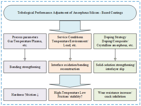
Figure 4.
Enhancement mechanism of tribological performance in amorphous silicon coatings. (The upward-pointing arrows indicate “increase” or “rise”; the downward-pointing arrows indicate “decrease” or “drop”).
3.1. Process–Structure Synergy in Governing Amorphous Silicon Tribology
Recent studies on performance optimization of amorphous silicon-based coatings have focused on regulating CVD process parameters—such as reactant gas ratios, temperatures, and plasma conditions—to systematically investigate their synergistic interaction mechanisms with coating microstructure, chemical bonding states, and mechanical properties. Research has demonstrated that precise parameter control not only optimizes coating densification and surface morphology but also significantly enhances hardness, elastic modulus, and tribological performance by reinforcing chemical bond networks and increasing cross-linking degrees.
According to Zhou and Persson et al. [72], coating surface roughness decreased with rising NH3/DCS flow ratio. Concurrently, mechanical properties improved, reaching a maximum of 27 GPa hardness and 290 GPa elastic modulus at a ratio of 4. Concurrently, the wear rate decreased significantly, accompanied by enhanced structural densification and surface smoothness. Their work revealed the critical influence mechanisms of the nitrogen-to-silicon ratio and temperature on Si-N bond formation, surface roughness, and mechanical performance. They demonstrated that optimized LPCVD parameters (flow ratio of 4; temperature of 790 °C) could significantly enhance the mechanical and wear-resistant properties of coatings. Employing RP-CVD, Wrobel and Uznanski et al. [28] synthesized a-SiCN:H coatings. They discovered that increasing nitrogen concentration and applying high-power plasma promoted the formation of silicon–nitride bonds and enhanced cross-linking density, resulting in denser amorphous networks. This structural evolution endowed the films with superior friction resistance and wear durability, attributed to their more uniform surfaces and tightly packed molecular chain architectures. Uznanski and Jankowski et al. [38] fabricated a-SiOC:H films via RPCVD. Their study showed that elevated substrate temperatures reduced Si-OH groups while increasing Si-O-Si groups, transitioning film properties from polymer-like to highly cross-linked materials. As the temperature increased from 100 °C to 350 °C, both the hardness and elastic modulus progressively rose, peaking at 350 °C. Concurrently, the friction coefficient decreased from 0.4 to 0.15, demonstrating temperature-driven optimization of mechanical and tribological performance. Wu and Qiu et al. [73] demonstrated that by embedding nanocrystals in amorphous SiNx, this structure combines the strengthening effect of nanocrystalline grains and the toughness of amorphous matrix, making the coating maintain high hardness while also having good fracture toughness. Cutini and Forghierio et al. [74] generated disordered structures by thermal annealing of α quartz crystals and passivate surface dangling bonds to form silanol groups (Si-OH), and simulated real surfaces by regulating silanol density and distribution (exposed or buried). High silanol density enhances interfacial chemical reactions, which intensifies adhesive friction, while low density or hydrogenation/oxidation passivation can inhibit the formation of chemical bonds and reduce friction. Long and Wang et al. [75] increased the densification degree of the film by increasing the magnetron sputtering power, and the density of Si-C bonds increased, which enhanced the structural rigidity of the amorphous network, while the internal residual compressive stress inhibited crack propagation; in addition, the decrease in the sp3/sp2 ratio indicates that carbon atoms tend to graphitize, which can form a lubricating layer during the friction process, reducing the friction coefficient and adhesive wear.
In summary, during the preparation of amorphous silicon-based nitride coatings, the control of stoichiometry, primarily through regulating the nitrogen-to-silicon (N/Si) atomic ratio via precise adjustment of the NH3/DCS flow ratio, is a critical factor governing coating performance. Optimizing process parameters—such as increasing the NH3/DCS flow ratio to 4, elevating nitrogen concentration, enhancing plasma power, and raising the deposition temperature to 790 °C—significantly promotes the formation of Si-N bonds and strengthens structural cross-linking. This stoichiometric control directly influences key coating parameters: a well-optimized N/Si ratio increases the density of Si-N covalent bonds, thereby improving coating densification and surface finish by minimizing voids and irregularities at the atomic scale. These optimizations not only improve coating densification and surface finish but also achieve high hardness and elastic modulus, along with a reduced friction coefficient (0.15), demonstrating exceptional wear resistance. The study further elucidates the synergistic mechanisms among nitrogen-to-silicon (N/Si) ratio regulation, temperature field control, and bonding structure evolution.
3.2. Tribochemical Response Modulation Under Operational Stress States
The tribological performance of amorphous silicon-based coatings is governed by multidimensional operational parameters, with their governing mechanisms involving complex processes such as interfacial oxidation reactions, chemical bond reconstruction, and stress field distribution.
Zeng and Qin et al. [76] observed ultralow friction in a-Si:H coatings deposited on high-speed tool steel under elevated temperatures. They attributed this phenomenon to oxides generated via high-temperature oxidation. At 600 °C, the amorphous silicon film exhibited an ultralow friction coefficient (0.07), attributed to the formation of α − Fe2O3/SiO2 composite oxides through thermal oxidation. Comparative studies of different counter-face materials revealed that ceramic materials demonstrate superior stability and lower initial friction coefficients at high temperatures, making them ideal counterparts for amorphous silicon films. Mangolini and Koshigan et al. [77] investigated ambient atmosphere effects on a-C:H:Si:O coating tribology. As shown in Figure 5, in a hydrogen environment, hydrogen molecules react with strained sp2 carbon–carbon bonds on the a-C:H:Si:O surface, generating a hydrogenated amorphous carbon layer rich in C-H groups. This surface layer exhibits reduced shear strength, thereby lowering both friction coefficient and wear rate. Conversely, in an oxygen environment, strained sp2 carbon–carbon bonds react with oxygen molecules, leading to further oxidation of silicon atoms while simultaneously forming carbonyl/ether groups. These oxidation products increase the shear strength of interfacial materials, thereby elevating friction coefficient and wear rate with increasing oxygen pressure.
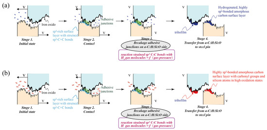
Figure 5.
Tribochemical response mechanism of steel/a-C:H:Si:O interfaces under (a) oxygen (b) atmosphere [78].
While the choice of counter-face material is crucial for optimizing friction under specific conditions like high temperature, the intrinsic properties and composition of the coating itself also play a fundamental role in determining its overall tribological performance, including wear resistance under varying loads. Beake and McMaster et al. [79] developed Si-DLC coatings. These coatings exhibited lower wear rates under low-load/high-contact-radius conditions due to their enhanced hardness. Under high-load/low-contact-radius conditions, Si-DLC coatings effectively resisted microcrack initiation and propagation. Furthermore, they maintained low friction coefficients and stable wear behavior across varying humidity levels. Jiang and Guo et al. [80] successfully prepared a-C:H:Si:O coatings on PEEK substrates using RF-PECVD technology. Compared to untreated PEEK, the coatings significantly increased surface hardness and reduced wear rates by over tenfold. The study demonstrated that optimized silicon and oxygen doping levels effectively enhance mechanical properties and friction film formation, thereby reducing friction coefficients and wear rates while improving wear resistance and lubrication performance in PEEK/metal sliding assemblies. These superior tribological properties are clearly demonstrated in Figure 6 which shows the lower friction coefficient of the a-C:H:Si:O coating.
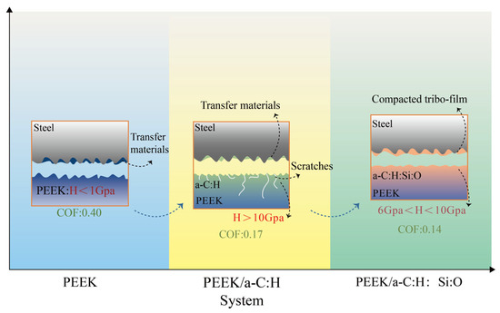
Figure 6.
Fundamental wear mechanisms across material systems [80].
3.3. Friction-Wear Synergy Mediated by Dopant-Induced Bond Reconstruction
The optimization of the tribological performance of amorphous silicon-based coatings can be achieved through strategies of material compositing and structural control. The underlying mechanisms encompass multi-scale processes such as chemical bond reconstruction, hetero-interface effects, and phase transformation synergy.
Utilizing closed-field unbalanced magnetron sputtering, Wu and Wang et al. [81] incorporated trimethyl silane (TMS) dopant into CrSiCN coatings. This silicon doping induced lattice distortion and concurrently facilitated the precipitation of amorphous silicon nitride (a-Si3N4) and silicon carbide (a-SiC) phases. Consequently, coating hardness rose from 18.1 GPa to 21.3 GPa, attributed to solid solution strengthening, alongside concurrent enhancements in friction coefficient and wear rate.
Zeng and Ning et al. [82] employed 3-(aminopropyl) triethoxysilane (APTES) as a coupling agent to self-assemble WS2/GO (tungsten disulfide/graphene oxide) films onto hydroxylated amorphous silicon (a-Si) surfaces. This assembly, mediated by Si-O-Si and C-N-C bond formation, yielded a composite coating exhibiting a 0.09 reduction in friction coefficient relative to pure GO films. Wear track analysis revealed that WS2 incorporation expanded the interlayer spacing within GO and enhanced interlayer shear capability in the resulting WS2/GO tribofilm, leading to superior friction reduction compared to GO alone. Further exploring WS2 enhancement, Zeng and Ning et al. [83] developed low-shear-stress WS2 nanosheet coatings on amorphous silicon substrates via drop-casting, creating WS2/a-Si composites. Tribological evaluation using an RTEC multifunctional tribometer under disk-on-disk configuration revealed a dramatic friction coefficient reduction from 0.5 to 0.08. As illustrated in Figure 7, this ultralow friction originates from (i) the in situ formation of WS2 lubricious transfer films at ball wear scars and (ii) interfacial heterojunction effects at WS2/a-Si boundaries, collectively establishing asymmetric contact geometries that stabilize friction dissipation.
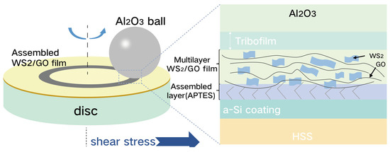
Figure 7.
Schematic illustration of the lubrication mechanism for the assembled WS2/GO film on a-Si coating [82].
Sun et al. [47] prepared thin films with varying silicon content using electron cyclotron resonance plasma sputtering and conducted structural, mechanical, and tribological characterizations. The results indicated that silicon doping preferentially combined with sp3 carbon bonds, enhancing the film hardness and significantly reducing the friction coefficient to as low as 0.02. The reduction in friction was attributed to the formation of hydrogen bonds due to the passivation effect of -OH or -H groups by silicon atoms at the sliding interface, as well as the π*-π* interaction between graphene layers. Sha and Lukianov et al. [30] prepared carbon-rich amorphous silicon carbide (a-SiC:H) and silicon carbon nitride (a-SiCN:H) films on amorphous silicon substrates using PECVD. Both films exhibited high hardness, high elastic modulus, low surface roughness, and high uniformity, with a hardness-to-elastic modulus ratio (H/E) greater than 0.13, significantly improving the wear resistance of the films.
Ju and Zhou et al. [84] added amorphous SiNx to Mo2N/Cu films, increasing the film hardness from approximately 17 GPa to 30 GPa. In RT−500 °C temperature cycling wear tests, the addition of amorphous SiNx restricted the increase in dislocations within the grains and the propagation of microcracks at the interfaces, demonstrating excellent wear resistance. Similarly, Jamet [85] significantly enhanced coating hardness and elastic modulus by forming a nanocomposite structure of amorphous Si3N4 and polycrystalline AlN. The chemical inertness and dense structure of amorphous Si3N4 reduced abrasive wear, decreasing wear volume by 60% under 2N load through fragmentation and particle pull-out mechanisms, while its homogeneous phase structure dispersed local stress and delayed crack propagation, and acted as a dense barrier against corrosive media.
Focusing on interface engineering, Lakhonchai and Chinsungnoen et al. [86] improved the adhesion of DLC coatings by introducing hydrogen into the a-Si:H interlayer to reduce oxygen and Si-O bond formation while increasing hardness and structural density, effectively reducing delamination risk and plastic deformation during friction.
In summary, the doping modification with rare elements can significantly regulate the micro-mechanical properties and tribological behavior of amorphous silicon-based coatings. By optimizing intrinsic mechanical parameters such as the hardness and elastic modulus of the coating system, and simultaneously reducing the interfacial friction coefficient, the element doping strategies enhance the mechanical load-bearing capacity of the coating. Additionally, these strategies induce a surface friction dissipation synergistic effect, thereby achieving a systematic improvement in wear resistance under complex stress conditions.
3.4. Synthesis of Process–Structure–Property Relationships
The tribological properties of amorphous silicon-based coatings are fundamentally determined by the interdependent effects of deposition process parameters, atomic-scale bonding configurations, and microstructural characteristics. Explicit dependencies connect governing parameters—including the nitrogen-to-silicon ratio, deposition temperature, plasma power, and dopant concentration—to critical performance metrics such as surface morphology, mechanical properties, and tribological responses.
The nitrogen-to-silicon ratio stands out as a particularly potent and multifunctional governing parameter. Increasing this ratio during deposition processes like CVD significantly promotes the formation of silicon–nitrogen bonds within the amorphous network. This enhanced Si-N bonding directly drives an increase in the cross-linking density of the coating structure. The consequences of this densification are multifaceted and beneficial for tribological performance. Firstly, it leads to a noticeable reduction in surface roughness, minimizing asperity contact and the initiation of abrasive wear. Secondly, the rigid covalent Si-N network substantially elevates the coating’s hardness and elastic modulus, enhancing its resistance to plastic deformation under contact stress. Thirdly, the combination of a smoother surface and a harder, more cohesive structure translates directly into a lower friction coefficient by impeding adhesive shear forces at the sliding interface. Thus, optimizing the nitrogen-to-silicon ratio acts through a clear mechanistic chain: it fosters stronger Si-N bonds, which create a denser and more robust amorphous network, ultimately yielding superior surface quality, mechanical strength, and friction reduction.
Substrate temperature exerts a profound influence on chemical bonding states and defect populations. Lower deposition temperatures tend to favor the presence of Si-OH groups, imparting a more polymer-like character to the film with consequently higher friction coefficients. Raising the temperature facilitates the conversion of these Si-OH groups into Si-O-Si linkages, increasing the network’s cross-linking density. This structural evolution enhances both hardness and elastic modulus while simultaneously lowering the friction coefficient. However, excessively high temperatures become detrimental, triggering hydrogen effusion from the structure and leaving behind reactive dangling bonds. This degradation can lead to subsurface damage mechanisms, such as hydrogen bubble formation and eventual interfacial delamination, severely compromising coating integrity and performance.
Plasma power in techniques like PECVD presents a critical balance. Moderate power levels effectively enhance the dissociation of precursor gases and promote the formation of strong Si-C and Si-N bonds, thereby increasing coating hardness and wear resistance. However, excessive power introduces significant risks. The intense ion bombardment associated with high power can drive hydrogen deep into the coating or substrate interface, where it accumulates to form pressurized H2 bubbles. Upon reaching a critical pressure, these bubbles can rupture catastrophically, causing micro-explosions that lead to blistering and delamination of the film.
Strategic elemental doping offers powerful pathways to tailor tribochemical responses and interfacial behavior. Incorporating elements like silicon into matrices such as CrCN induces lattice distortion and can facilitate the precipitation of beneficial secondary amorphous phases like silicon nitride and silicon carbide. This multiphase structure enhances hardness through solid solution strengthening and dispersion hardening, improving both friction and wear characteristics. Similarly, depositing nanocomposite layers such as WS2/GO onto amorphous silicon surfaces creates interfaces with unique tribochemical activity. The presence of tungsten disulfide expands the interlayer spacing within graphene oxide and enhances interlayer shear capability within the resulting transfer film. This, combined with interfacial heterojunction effects, establishes asymmetric contact geometries that effectively stabilize friction dissipation, leading to dramatically reduced friction coefficients. Furthermore, incorporating oxygen into amorphous carbon matrices significantly boosts corrosion resistance by enhancing electrical insulation, reducing porosity, and increasing hydrophobicity. This multifunctional barrier effect protects the underlying substrate while maintaining favorable tribological properties under corrosive conditions.
Performance trade-offs and unresolved mechanistic chains require careful consideration. While high cross-linking density achieved through parameters like increased N/Si ratio or temperature improves hardness, it can simultaneously increase brittleness unless mitigated by strategies such as embedding nanocrystalline phases within the amorphous matrix. Catalytic CVD enables crucial low-temperature deposition but faces challenges related to potential catalyst contamination and its impact on long-term stability. The friction behavior of coatings, particularly those containing carbon, is highly sensitive to the operating atmosphere; environments rich in hydrogen can passivate surfaces and lower friction, whereas oxygen promotes oxidation and increases shear strength and friction. Finally, the precise mechanisms governing the evolution of in situ tribofilms and the quantitative contribution of different bond reconstructions under dynamic sliding conditions remain areas needing deeper investigation through advanced in situ characterization techniques.
4. Passivation Network Reconstruction: Corrosion Protection Mechanisms in Amorphous Architectures
Amorphous silicon-based coatings exhibit significant advantages in corrosion resistance due to their unique structure characterized by short-range order and long-range disorder. This structure effectively eliminates crystal defects such as grain boundaries and dislocations, thereby significantly reducing the pathways for corrosive media to penetrate along grain boundaries [87,88,89,90].
Furthermore, the dominant strong covalent bond network (Si-Si/Si-M bonds, where M represents transition metal elements) in amorphous silicon compounds has high bond energy and directionality, forming a dense passivation film. This film reduces the density of surface active sites and inhibits the charge transfer process, thereby hindering the synergistic occurrence of anodic metal dissolution and cathodic hydrogen evolution reactions [91,92,93,94,95].
Additionally, the uniformly distributed alloy elements in the amorphous phase form stable metal–silicon covalent bonds, which can regulate the semiconductor properties of the surface oxide film and enhance its chemical stability in corrosive media such as Cl− [96,97,98,99].
Experimental studies by Yin and Liu et al. [100] have shown that SiCOH coatings with a-C:H:SiOx top layers exhibit significantly better corrosion protection performance on various substrates compared to pure a-C:H coatings (HDLC). The a-C:H:SiOx top layer enhances electrical insulation by increasing sp3 carbon hybridization, forms insulating silicon oxide to block corrosive media, reduces coating porosity to minimize diffusion pathways, improves heterostructure to compensate for underlying defects, and increases surface hydrophobicity to reduce media adhesion. These mechanisms significantly improve the corrosion resistance of the coating, demonstrating excellent protective effects on different substrates. Topka and Diallo et al. [101] prepared amorphous SiOxNy films via chemical vapor deposition. When tested in buffered oxide etch containing hydrofluoric acid, the introduction of nitrogen enhanced the film’s network structure, making it more compact and stable, effectively blocking the penetration of corrosive media. When the nitrogen content exceeds 7 at. %, the etch rate drops to an extremely low level (0.1 Å/s).
While the unique amorphous structure and chemical bond characteristics fundamentally underpin the corrosion resistance of these coatings, their actual protective performance in practical service environments requires systematic validation. Performance differences and optimization directions require further elucidation through rigorous evaluation under diverse corrosive conditions. Researchers have conducted studies on corrosion kinetics and surface behavior across various material systems. Combining electrochemical parameter analysis with microscopic morphology observations facilitates the revelation of intrinsic relationships between coating composition, structural design, and environmental adaptability. Manj and Zhang et al. [102] prepared a-Si:H interlayers via DC magnetron sputtering. The presence of hydrogen reduces oxide formation at the interface, thereby improving the bonding strength between the interlayer and substrate. Additionally, hydrogen removes the oxide layer on the chromium coating surface, promoting bonding between Si-C and Cr-Si. The strong adhesion between the a-Si:H interlayer and metal substrate further enhances corrosion resistance. Delimi and Ferkous et al. [103] conducted argon plasma pretreatment on the substrate before depositing amorphous a-SiOx films. The optimized coating displayed a contact angle of 117° ± 2°, demonstrating significantly enhanced hydrophobicity. Electrochemical tests showed that pretreated samples tested in 3.5 wt.% NaCl solution exhibited a more positive stable open-circuit potential, lower corrosion current density, and higher low-frequency impedance magnitude. After 30 days of immersion, the argon-pretreated coating maintained 81% corrosion protection efficiency, verifying the synergistic improvement in interfacial adhesion quality and barrier performance. Table 4 lists typical experimental data, which can more directly illustrate the specific performance and influencing factors of the aforementioned theoretical mechanisms in actual corrosion protection.
Table 4.
Corrosion resistance of different amorphous silicide.
Based on the analysis of the corrosion protection mechanisms presented in the table, the key aspects can be summarized as follows:
- Elimination of Anisotropic Defects
The unique short-range ordered/long-range disordered atomic structure of amorphous silicon fundamentally underpins its exceptional corrosion resistance. This structure eliminates inherent crystalline defects such as grain boundaries and dislocations, which in crystalline materials serve as preferential pathways for corrosive media (e.g., Cl− and H+ ions) to penetrate and rapidly diffuse. By obstructing these pathways, the amorphous architecture significantly retards the diffusion rate of corrosive agents into the coating and substrate, substantially enhancing the barrier performance.
- ii.
- Robust Covalent Bond Network and Dense Passivation Film Formation
Amorphous silicon compounds are primarily composed of a three-dimensional network of high-bond-energy, directionally strong covalent bonds. This intrinsically dense network rapidly reconstructs into a continuous, compact, and chemically stable passivation film in corrosive environments. This film reduces the density of active sites for corrosion reactions on the coating surface, suppresses the charge transfer processes critical to anodic metal dissolution and cathodic hydrogen evolution reactions, and acts as a physical barrier against the penetration of corrosive media.
- iii.
- Optimization of Passivation Film Properties via Elemental Doping
Uniformly distributed alloying elements form stable covalent bonds with silicon, effectively modulating the semiconductor properties of the surface oxide passivation film, such as reducing defect state density, and enhancing its chemical stability in aggressive media, particularly Cl−-containing environments. Nitrogen doping, especially above a threshold concentration (>7 at. %), strengthens and stabilizes the amorphous network structure, rendering the coating exceptionally dense. This effectively blocks the penetration of corrosive media (e.g., hydrofluoric acid) and reduces corrosion/etching rates to ultralow levels. Silicon oxides (SiOx) contribute through multiple mechanisms: they enhance electrical insulation (via increased sp3 carbon hybridization or intrinsic insulating properties) to disrupt electrochemical corrosion circuits; improve structural densification and reduce porosity to inhibit diffusion pathways; and increase hydrophobicity to minimize wetting and adhesion of corrosive liquids. Collectively, these effects establish a multifunctional physico-chemical barrier against corrosion.
In summary, the introduction of silicon oxides or nitrogen elements into composite coating systems can further enhance electrical insulation, densification, and hydrophobic properties. Through the synergistic action of multiple mechanisms, these coatings can effectively block corrosion pathways. The dense network structure of nitrogen-doped amorphous films significantly reduces the penetration rate of corrosive media. Relevant studies have revealed the intrinsic relationships between coating composition, structural design, and environmental adaptability through electrochemical analysis and microscopic characterization, providing theoretical support for optimizing corrosion resistance.
5. Conclusions and Future Research Directions
5.1. Conclusions
CVD technology, due to its process flexibility and controllability of microstructure, has become an important method for preparing high-performance amorphous silicon coatings. Through the optimization of different processes such as HWCVD, PECVD, and CCVD, precise control can be achieved in terms of coating density (with a maximum hardness of up to 27 GPa), surface roughness (Ra < 0.1 µm), and chemical bonding state (Si-N bond ratio > 60%). Amorphous silicon-based coatings exhibit significant advantages in tribological performance. For example, the friction coefficient of a WS2/GO composite system can be as low as 0.08, and the wear rate of Si-DLC coatings can be reduced by over 90%. The corrosion resistance mechanism of these coatings stems from the isotropic characteristics of the amorphous structure and the strong covalent bond network. Typical coatings can achieve a corrosion current density as low as 4.2 × 10⁻⁴ µA/cm2 in a 3.5% NaCl solution, with the passivation range extending to 0.6 V.
5.2. The Current Resources Are Insufficient
Despite the significant potential of amorphous silicon nitride coatings in the field of bearing steel surface modification, their large-scale application still faces multidimensional challenges:
- Inadequate Deepening of Process Optimization Mechanisms: Current research predominantly employs a “trial-and-error” approach for parameter optimization, lacking systematic theoretical models based on reaction kinetics and mass transfer processes.
- Insufficient Adaptability to Complex Operating Conditions: Existing performance tests are often limited to standard laboratory conditions, with inadequate assessment of the effects of extreme temperatures, high pressures, and corrosive media acting in concert.
- Lack of Long-term Stability Studies: There is a deficiency in the quantitative characterization of the structural evolution of coatings under cyclic thermal and mechanical loads.
- Prominent Contradictions in Environmental Friendliness: Some precursors (such as SiH4) pose risks of flammability and explosion, and high-temperature processes consume significant amounts of energy.
- Inadequate Analysis of Failure Mechanisms: The cross-scale correlation research on interface failure and tribological chemical reactions has yet to form a complete theoretical system.
5.3. Future Outlook
- Intelligent Process Development: The transition from empirical optimization to machine learning (ML)-driven intelligent process design represents a critical frontier for advancing CVD-fabricated amorphous silicon coatings. Future research should establish comprehensive ML frameworks—leveraging Bayesian optimization, convolutional neural networks, and generative adversarial networks—to decode complex relationships between deposition parameters, microstructural characteristics, and functional performance. By curating multi-source datasets from in situ diagnostics and post-deposition characterization, these models can predict outcomes like Si-N bond formation efficiency or sp3 carbon content with high fidelity. Crucially, this enables inverse design: specifying target properties to autonomously generate optimal process recipes. Implementing such systems requires embedding ML controllers within CVD reactors for real-time adjustment of RF power modulation or precursor pulse sequences during deposition. To overcome data scarcity, transfer learning and synthetic data generation will accelerate training. Validating these AI workflows via combinatorial experiments will replace costly trial-and-error, establishing predictive synthesis for HWCVD, PECVD, and CCVD platforms. This enables bespoke coatings for extreme environments while significantly reducing development cycles.
- The thermal–mechanical–chemical multi-field coupling effect on amorphous silicon-based coatings is not a simple superposition of individual field actions but a complex dynamic interplay that accelerates failure mechanisms. To address this, in situ testing platforms should be tailored to simulate extreme service scenarios, integrating dynamic temperature control, precision mechanical loading systems, and corrosive medium circulation modules. Such platforms will capture real-time changes in critical parameters, for instance, tracking how thermal stress-induced microcracks facilitate corrosive ion penetration, while chemical etching weakens the coating’s load-bearing capacity, ultimately accelerating wear. This research will establish a mapping relationship between multi-field parameters and failure modes, identifying critical thresholds such as the temperature at which thermal softening exacerbates mechanical fatigue or the stress intensity factor governing corrosion-induced crack propagation. These insights are pivotal for optimizing coating designs. For instance, introducing gradient compositions can mitigate thermal stress gradients, while doping specific elements enhances the passivation film’s resistance to tribochemical damage. Such optimizations are essential for improving component reliability within complex service environments.
- The construction of novel composite systems, such as MXene/amorphous silicon heterostructures and gradient doping, represents a pivotal direction to overcome the inherent limitations of single-phase amorphous silicon coatings and synergistically enhance their tribological and corrosion-resistant performances. MXenes, as a class of two-dimensional transition metal carbides/nitrides with excellent electrical conductivity, mechanical flexibility, and chemical stability, can form unique heterointerfaces with amorphous silicon coatings. This heterostructure is expected to leverage the high strength and corrosion barrier properties of amorphous silicon while utilizing MXene’s surface functional groups to strengthen interfacial bonding, thereby mitigating coating delamination under mechanical loading. Additionally, MXene’s lamellar structure can act as a “lubricating interlayer” to reduce friction coefficients, while its electrochemical activity may promote the formation of a more stable passivation film in corrosive environments, inhibiting localized corrosion.
Gradient doping, by contrast, enables a controlled variation in chemical composition and microstructure along the coating thickness, addressing the mismatch in thermal expansion and mechanical properties between the coating and substrate. For instance, introducing a gradient distribution of nitrogen or carbon in amorphous silicon-based coatings can gradually enhance the hardness and wear resistance of the surface layer while maintaining good adhesion at the interface through a relatively ductile transition zone. This design not only suppresses crack initiation at the interface caused by thermal–mechanical coupling but also optimizes the density of the passivation film, as higher nitrogen content near the surface can form a more compact Si-N network to resist corrosive ion penetration. Such composite systems, through the rational integration of multi-component synergies and structural gradients, hold great promise for expanding the application of amorphous silicon coatings in extreme environments requiring both high wear resistance and long-term corrosion protection, such as marine engineering and high-temperature mechanical components.
- iv.
- Enhancing the environmental adaptability of amorphous silicon-based coatings fabricated via CVD necessitates a dual focus on low-temperature process development and the adoption of green precursors, addressing both substrate compatibility and sustainability challenges. Traditional CVD processes often require elevated temperatures (>300 °C) to achieve dense, high-quality coatings, limiting their application to thermally robust substrates and consuming excessive energy. Developing low-temperature processes (<200 °C), such as plasma-enhanced atomic layer deposition (PE-ALD), can overcome this constraint: plasma activation lowers the activation energy of precursor reactions, enabling the formation of dense amorphous networks at mild temperatures while maintaining precise thickness control and conformal coverage—critical for heat-sensitive substrates like polymers, flexible electronics, and biomaterials. This temperature reduction not only expands the coating’s applicability across diverse environments but also reduces energy consumption, aligning with global carbon neutrality initiatives.
Complementing low-temperature processes, the shift to green precursors—such as liquid silicon sources—addresses safety and environmental concerns associated with conventional gaseous precursors like silane (SiH4), which are highly flammable and toxic. Liquid silicon sources offer improved handling stability, reduced volatility, and lower environmental impact during storage and deposition. When coupled with PE-ALD, these precursors facilitate controlled dissociation and surface reactions, ensuring the formation of defect-free amorphous structures with tailored chemical bonding that enhance corrosion resistance and tribological performance in harsh environments. Together, low-temperature PE-ALD and green liquid silicon sources enable the fabrication of high-performance amorphous silicon coatings that are both environmentally benign and adaptable to a broader range of substrates, bridging the gap between technological performance and sustainable manufacturing practices.
- v.
- Establishing a multi-scale lifespan prediction model for amorphous silicon-based coatings, integrating molecular dynamics (MD) simulations and finite element analysis (FEA), is critical for bridging the gap between fundamental material properties and practical service durability. MD simulations, operating at the atomic scale, can capture intrinsic processes such as the diffusion of corrosive ions through amorphous networks, the breaking and reconstruction of Si-Si/Si-O bonds under thermal stress, and the evolution of interfacial defects that initiate failure. These atomic-level insights—including activation energies for defect formation and diffusion coefficients—provide essential parameters for understanding microscale degradation mechanisms, such as passivation film breakdown or interfacial delamination.
Complementing MD, FEA operates at the macroscale to model the coating–substrate system under complex service conditions, incorporating mechanical loads, thermal gradients, and chemical environments. By inputting MD-derived material properties into FEA frameworks, the model can predict macroscopic failure behaviors, such as crack propagation paths, stress concentration-induced wear acceleration, or coating thinning due to synergistic corrosion and abrasion. This multi-scale integration enables quantitative prediction of service life under specific operating conditions, identifying critical factors that dictate coating longevity.
Funding
This research received no external funding.
Conflicts of Interest
The authors declare no conflict of interest.
References
- Ma, M.; Qi, Y.; Zhang, C.; Chen, Q.; Gu, C.; Zhang, Z. Highly efficient antifouling and toughening hydrogel for ship coatings. Appl. Surf. Sci. 2024, 662, 160102. [Google Scholar] [CrossRef]
- Thomas, P.; Sahoo, B.N.; Thomas, P.J.; Greve, M.M. Recent advances in emerging integrated anticorrosion and antifouling nanomaterial-based coating solutions. Environ. Sci. Pollut. Res. 2024, 31, 67550–67576. [Google Scholar] [CrossRef]
- Pei, W.; Pei, X.; Xie, Z.; Wang, J. Research progress of marine anti-corrosion and wear-resistant coating. Tribol. Int. 2024, 198, 109864. [Google Scholar] [CrossRef]
- Liang, H.; Shi, X.; Li, Y. Technologies in Marine Antifouling and Anti-Corrosion Coatings: A Comprehensive Review. Coatings 2024, 14, 1487. [Google Scholar] [CrossRef]
- Choi, M.; Novak, T.G.; Byen, J.; Lee, H.; Baek, J.; Hong, S.; Kim, K.; Song, J.; Shin, H.; Jeon, S. Significantly Enhanced Thermoelectric Performance of Graphene through Atomic-Scale Defect Engineering via Mobile Hot-Wire Chemical Vapor Deposition Systems. ACS Appl. Mater. Interfaces 2021, 13, 24304–24313. [Google Scholar] [CrossRef]
- Igumenov, I.K.; Lukashov, V.V. Modern Solutions for Functional Coatings in CVD Processes. Coatings 2022, 12, 1265. [Google Scholar] [CrossRef]
- Zheng, J.; Ye, L.; He, M.; He, D.; Huang, Y.; Yu, J.; Chen, T. Electrical and optical properties of amorphous silicon carbide thin films prepared by e-beam evaporation at room temperature. J. Non-Cryst. Solids 2022, 576, 121233. [Google Scholar] [CrossRef]
- Kaloyeros, A.E.; Arkles, B. Silicon Carbide Thin Film Technologies: Recent Advances in Processing, Properties, and Applications-Part I Thermal and Plasma CVD. ECS J. Solid State Sci. Technol. 2023, 12, 103001. [Google Scholar] [CrossRef]
- Zhang, X.; Lai, J.; Gray, T. Recent progress in low-temperature CVD growth of 2D materials. Oxf. Open Mater. Sci. 2023, 3, itad010. [Google Scholar] [CrossRef]
- Wang, X.; Yushin, G. Chemical vapor deposition and atomic layer deposition for advanced lithium ion batteries and supercapacitors. Energy Environ. Sci. 2015, 8, 1889–1904. [Google Scholar] [CrossRef]
- Hoque, A.; George, A.; Ramachandra, V.; Najafidehaghani, E.; Gan, Z.; Mitra, R.; Zhao, B.; Sahoo, S.; Abrahamsson, M.; Liang, Q.; et al. All-2D CVD-grown semiconductor field-effect transistors with van der Waals graphene contacts. npj 2D Mater. Appl. 2024, 8, 55. [Google Scholar] [CrossRef]
- Choi, M.; Baek, J.; Zeng, H.; Jin, S.; Jeon, S. Toward high-quality graphene film growth by chemical vapor deposition system. Curr. Opin. Solid State Mater. Sci. 2024, 31, 101176. [Google Scholar] [CrossRef]
- Xiao, M.; Gao, H.; Sun, L.; Wang, Z.; Jiang, G.; Zhao, Q.; Guo, C.; Li, L.; Jiang, F. Microstructure and mechanical properties of Fe-based amorphous alloy coatings prepared by ultra-high speed laser cladding. Mater. Lett. 2021, 297, 130002. [Google Scholar] [CrossRef]
- Koga, G.; Travessa, D.; Zepon, G.; Coimbrão, D.; Jorge, A.; Berger, J.; Roche, V.; Lepretre, J.-C.; Bolfarini, C.; Kiminami, C.; et al. Corrosion resistance of pseudo-high entropy Fe-containing amorphous alloys in chloride-rich media. J. Alloys Compd. 2021, 884, 161090. [Google Scholar] [CrossRef]
- Sabzi, M.; Anijdan, S.H.M.; Shamsodin, M.; Farzam, M.; Hojjati-Najafabadi, A.; Feng, P.; Park, N.; Lee, U. A Review on Sustainable Manufacturing of Ceramic-Based Thin Films by Chemical Vapor Deposition (CVD): Reactions Kinetics and the Deposition Mechanisms. Coatings 2023, 13, 188. [Google Scholar] [CrossRef]
- Chen, Y.; Fang, F.; Zhang, N. Advance in additive manufacturing of 2D materials at the atomic and close-to-atomic scale. npj 2D Mater. Appl. 2024, 8, 17. [Google Scholar] [CrossRef]
- Tian, Y.; Yan, Z.; Jiang, L.; Liu, R.; Liu, B.; Shao, Y.; Yang, X.; Liu, M. Multiscale Models of CVD Process: Review and Prospective. Materials 2024, 17, 5131. [Google Scholar] [CrossRef] [PubMed]
- Ohmagari, S. Single-crystal diamond growth by hot-filament CVD: A recent advances for doping, growth rate and defect controls. Funct. Diam. 2023, 3, 2259941. [Google Scholar] [CrossRef]
- Feng, X.; Yuan, X.; Zhou, J.; An, K.; Zhu, F.; Wei, X.; Huang, Y.; Zhang, J.; Chen, L.; Liu, J.; et al. A review: CNT/diamond composites prepared via CVD and its potential applications. Mater. Sci. Semicond. Process. 2024, 186, 109008. [Google Scholar] [CrossRef]
- Sreejith, S.; Ajayan, J.; Kollem, S.; Sivasankari, B. A Comprehensive Review on Thin Film Amorphous Silicon Solar Cells. Silicon 2022, 14, 8277–8293. [Google Scholar] [CrossRef]
- Greenhorn, S.; Bano, E.; Stambouli, V.; Zekentes, K. Amorphous SiC Thin Films Deposited by Plasma-Enhanced Chemical Vapor Deposition for Passivation in Biomedical Devices. Materials 2024, 17, 1135. [Google Scholar] [CrossRef] [PubMed]
- Qiu, D.; Lambertz, A.; Duan, W.; Mazzarella, L.; Wagner, P.; Morales-Vilches, A.B.; Yang, G.; Procel, P.; Isabella, O.; Stannowski, B.; et al. A Review: Application of Doped Hydrogenated Nanocrystalline Silicon Oxide in High Efficiency Solar Cell Devices. Adv. Sci. 2024, 11, e2403728. [Google Scholar] [CrossRef]
- Lu, B.; Zhuge, F.; Zhao, Y.; Zeng, Y.-J.; Zhang, L.; Huang, J.; Ye, Z.; Lu, J. Amorphous oxide semiconductors: From fundamental properties to practical applications. Curr. Opin. Solid State Mater. Sci. 2023, 27, 101092. [Google Scholar] [CrossRef]
- Ohring, M. Materials Science of Thin Films: Depositon and Structure; Academic Press: Cambridge, MA, USA, 2002. [Google Scholar]
- Pierson, H.O. Handbook of Chemical Vapor Deposition: Principles, Technology and Applications; William Andrew: Norwich, NY, USA, 1999. [Google Scholar]
- Wrobel, A.M.; Uznanski, P. Hard silicon carbonitride thin-film coatings produced by remote hydrogen plasma chemical vapor deposition using aminosilane and silazane precursors. 1: Deposition mechanism, chemical structure, and surface morphology. Plasma Process. Polym. 2021, 18, e2000240. [Google Scholar] [CrossRef]
- Ivashchenko, V.; Kozak, A.; Porada, O.; Ivashchenko, L.; Sinelnichenko, O.; Lytvyn, O.; Tomila, T.; Malakhov, V. Characterization of SiCN thin films: Experimental and theoretical investigations. Thin Solid Films 2014, 569, 57–63. [Google Scholar] [CrossRef]
- Wrobel, A.M.; Uznanski, P. Amorphous silicon carbonitride (a-SiCN) thin film coatings by remote plasma chemical vapor deposition using organosilicon precursor: Effect of substrate temperature. Plasma Process. Polym. 2022, 20, 2200190. [Google Scholar] [CrossRef]
- Xing, P.; Ma, D.; Ooi, K.J.A.; Choi, J.W.; Agarwal, A.M.; Tan, D. CMOS-Compatible PECVD Silicon Carbide Platform for Linear and Nonlinear Optics. ACS Photonics 2019, 6, 1162–1167. [Google Scholar] [CrossRef]
- Sha, B.; Lukianov, A.N.; Dusheiko, M.G.; Lozinskii, V.B.; Klyui, A.N.; Korbutyak, D.V.; Pritchin, S.E.; Klyui, N. Carbon-rich amorphous silicon carbide and silicon carbonitride films for silicon-based photoelectric devices and optical elements: Application from UV to mid-IR spectral range. Opt. Mater. 2020, 106, 109959. [Google Scholar] [CrossRef]
- Ma, X.; Xu, D.; Ji, P.; Jin, C.; Lin, J.; Ding, Y.; Xu, C. High-rate, room-temperature synthesis of amorphous silicon carbide films from organo-silicon in high-density helicon wave plasma. Vacuum 2019, 164, 355–360. [Google Scholar] [CrossRef]
- Kaloyeros, A.E.; Arkles, B. Review—Silicon Carbide Thin Film Technologies: Recent Advances in Processing, Properties, and Applications: Part II. PVD and Alternative (Non-PVD and Non-CVD) Deposition Techniques. ECS J. Solid State Sci. Technol. 2024, 13, 043001. [Google Scholar] [CrossRef]
- Zeng, Q.; Chen, T. Superlow friction and oxidation analysis of hydrogenated amorphous silicon films under high temperature. J. Non-Cryst. Solids 2018, 493, 73–81. [Google Scholar] [CrossRef]
- Müller, M.; Bouša, M.; Hájková, Z.; Ledinský, M.; Fejfar, A.; Drogowska-Horná, K.; Kalbáč, M.; Frank, O. Transferless Inverted Graphene/Silicon Heterostructures Prepared by Plasma-Enhanced Chemical Vapor Deposition of Amorphous Silicon on CVD Graphene. Nanomaterials 2020, 10, 589. [Google Scholar] [CrossRef]
- Ueda, Y.; Inoue, Y.; Shinohara, S.; Kawai, Y. Deposition of large area amorphous silicon films by ECR plasma CVD. Vacuum 1997, 48, 119–122. [Google Scholar] [CrossRef]
- Karar, P.; Kumar, G.; Wadibhasme, N.; Patil, D.S.; Dusane, R.O. Effect of Antenna-Substrate Distance on Quality of a-Si:H During ICP CVD Using a Flat Spiral Antenna. IEEE Trans. Plasma Sci. 2020, 49, 624–631. [Google Scholar] [CrossRef]
- Fischer, B.; Nuys, M.; Astakhov, O.; Haas, S.; Schaaf, M.; Besmehn, A.; Jakes, P.; Eichel, R.-A.; Rau, U. Advanced atmospheric pressure CVD of a-Si:H using pure and cyclooctane-diluted trisilane as precursors. Sustain. Energy Fuels 2024, 8, 5568–5580. [Google Scholar] [CrossRef]
- Uznanski, P.; Walkiewicz-Pietrzykowska, A.; Jankowski, K.; Zakrzewska, J.; Wrobel, A.M.; Balcerzak, J.; Tyczkowski, J. Atomic Hydrogen Induced Chemical Vapor Deposition of Silicon Oxycarbide Thin Films Derived from Diethoxymethylsilane Precursor. Appl. Organomet. Chem. 2020, 34, e5674. [Google Scholar] [CrossRef]
- Meng, H.; Wu, X.; Ma, F.; Zeng, Q.; Zhou, L. Structural optimization and growth of intrinsic hydrogenated amorphous silicon films by HWCVD. Sol. Energy Mater. Sol. Cells 2024, 271, 112835. [Google Scholar] [CrossRef]
- Oo, S.Z.; Tarazona, A.; Khokhar, A.Z.; Petra, R.; Franz, Y.; Mashanovich, G.Z.; Reed, G.T.; Peacock, A.C.; Chong, H.M.H. Hot-wire chemical vapor deposition low-loss hydrogenated amorphous silicon waveguides for silicon photonic devices. Photonics Res. 2019, 7, 193–200. [Google Scholar] [CrossRef]
- Wang, X.; Shen, X.; Gao, J.; Sun, F. Consecutive deposition of amorphous SiO2 interlayer and diamond film on graphite by chemical vapor deposition. Carbon 2017, 117, 126–136. [Google Scholar] [CrossRef]
- Xu, W.; Tang, H.; Zhang, Q.-Y.; Zhou, N.; Shen, Y. Room-temperature deposition of low H-content SiNx/SiNxOy thin films using a specially designed PECVD system. Surf. Coat. Technol. 2020, 402, 126506. [Google Scholar] [CrossRef]
- Jafari, S.; Linke, J.; Wendt, M.; Terheiden, B.; Meyer, S.; Lausch, D.; Steffens, J. Occurrence of Sharp Hydrogen Effusion Peaks of Hydrogenated Amorphous Silicon Film and Its Connection to Void Structures. Phys. Status Solidi (B) 2020, 257, 2000097. [Google Scholar] [CrossRef]
- Lukianov, A.N.; Klyui, N.I.; Sha, B.; Lozinskii, V.B.; Temchenko, V.P.; Avksentyeva, L.V.; Staschuk, V.S. Effect of discharge power and silicon content on optical and mechanical properties of carbon-rich amorphous silicon carbide films obtained by PECVD. J. Alloys Compd. 2019, 801, 285–294. [Google Scholar] [CrossRef]
- Lin, Y.; Feng, M.; Wang, Z.; Zeng, Y.; Liao, M.; Gong, L.; Yan, B.; Yuan, Z.; Ye, J. Excellent passivation with implied open-circuit voltage of 710 mV for p-type multi-crystalline black silicon using PECVD grown a-Si:H passivation layer. Sol. Energy 2020, 211, 753–758. [Google Scholar] [CrossRef]
- Li, M.; Jiang, L.; Sun, Y.; Xiao, T.; Xiang, P.; Tan, X. Synthesis and structural evolution of hydrogenated amorphous silicon carbide thin film with carbon nanostructures. J. Non-Cryst. Solids 2019, 503–504, 252–259. [Google Scholar] [CrossRef]
- Sun, K.; Wang, T.; Gong, W.; Lu, W.; He, X.; Eddings, E.G.; Fan, M. Synthesis and potential applications of silicon carbide nanomaterials / nanocomposites. Ceram. Int. 2022, 48, 32571–32587. [Google Scholar] [CrossRef]
- Shariah, A. Crystallization of Hydrogenated Amorphous Silicon Thin Films Using Combined Continuous Wave Laser and Thermal Annealing. Silicon 2024, 16, 4461–4470. [Google Scholar] [CrossRef]
- Özkol, E.; Procel, P.; Zhao, Y.; Mazzarella, L.; Medlin, R.; Šutta, P.; Isabella, O.; Zeman, M. Effective Passivation of Black Silicon Surfaces via Plasma-Enhanced Chemical Vapor Deposition Grown Conformal Hydrogenated Amorphous Silicon Layer. Phys. Status Solidi (RRL)—Rapid Res. Lett. 2019, 14, 1900087. [Google Scholar] [CrossRef]
- Kezzoula, F.; Kechouane, M.; Mohammed-Brahim, T.; Menari, H. Crystallization of P Type Amorphous Silicon (a-Si: H) by AIC Method: Effect of Aluminum Thickness. Silicon 2020, 12, 405–411. [Google Scholar] [CrossRef]
- Jarząbek, D.M.; Milczarek, M.; Nosewicz, S.; Bazarnik, P.; Schift, H. Size Effects of Hardness and Strain Rate Sensitivity in Amorphous Silicon Measured by Nanoindentation. Met. Mater. Trans. A 2020, 51, 1625–1633. [Google Scholar] [CrossRef]
- González, N.; García, T.; Morant, C.; Barrio, R. Fine-Tuning Intrinsic and Doped Hydrogenated Amorphous Silicon Thin-Film Anodes Deposited by PECVD to Enhance Capacity and Stability in Lithium-Ion Batteries. Nanomaterials 2024, 14, 204. [Google Scholar] [CrossRef]
- Du, T.; Li, W.; Li, W.; Li, J.; Xie, X. The Effect of the Dielectric Layer with Surface Plasma Treatment on Characteristics of Amorphous Silicon Antifuse. Electronics 2022, 11, 3522. [Google Scholar] [CrossRef]
- Mandal, S.; Dhar, S.; Das, G.; Mukhopadhyay, S.; Barua, A. Development of optimized n-μc-Si:H/n-a-Si:H bilayer and its application for improving the performance of single junction a-Si solar cells. Sol. Energy 2016, 124, 278–286. [Google Scholar] [CrossRef]
- Wu, C.-H.; Chang, K.-M.; Chen, Y.-M.; Zhang, Y.-X.; Tan, Y.-H. Investigation of Electrical Characteristics on AP-PECVD Fabricated Amorphous IGZO TFTs with Hydrogen Plasma Treatment. J. Nanosci. Nanotechnol. 2019, 19, 2306–2309. [Google Scholar] [CrossRef]
- Vivaldo, I.; Ambrosio, R.C.; López, R.; Flores-Méndez, J.; Sánchez-Gaspariano, L.A.; Moreno, M.; Candia, F. Enhanced Photoluminescence of Hydrogenated Amorphous Silicon Carbide Thin Films by Means of a Fast Thermal Annealing Process. Materials 2020, 13, 2643. [Google Scholar] [CrossRef] [PubMed]
- Li, M.; Jiang, L.; Sun, Y.; Wang, T.; Peng, Y.; Tian, H.; Xiao, T.; Xiang, P.; Tan, X. Correlation study of photoluminescence properties and mechanism of hydrogenated amorphous silicon carbide films. J. Lumin. 2019, 212, 38–44. [Google Scholar] [CrossRef]
- Kwon, S.; Park, Y.; Ban, W.; Youn, C.; Lee, S.; Yang, J.; Jung, D.; Choi, T. Effect of plasma power on properties of hydrogenated amorphous silicon carbide hardmask films deposited by PECVD. Vacuum 2020, 174, 109187. [Google Scholar] [CrossRef]
- Guler, I. Optical and structural characterization of silicon nitride thin films deposited by PECVD. Mater. Sci. Eng. B 2019, 246, 21–26. [Google Scholar] [CrossRef]
- Iliescu, C.; Chen, B.; Poenar, D.P.; Lee, Y.Y. PECVD amorphous silicon carbide membranes for cell culturing. Sens. Actuators B Chem. 2007, 129, 404–411. [Google Scholar] [CrossRef]
- Rashid, H.U.; Yu, K.; Umar, M.N.; Anjum, M.N.; Khan, K.; Ahmad, N.; Jan, M.T. Catalyst role in chemical vapor deposition (CVD) process: A review. Rev. Adv. Mater. Sci. 2015, 40, 235–248. [Google Scholar]
- Wang, Z.; Tu, H.T.C.; Ohdaira, K. Crystallization of catalytic CVD hydrogenated n-a-Si films on textured glass substrates by flash lamp annealing. Jpn. J. Appl. Phys. 2022, 61, SB1019. [Google Scholar] [CrossRef]
- Song, T.-H.; Hong, W.-S. Precipitation of Nanocrystallites in Amorphous Silicon Carbide Films by Low Temperature Catalytic CVD. ECS Meet. Abstr. 2013, MA2013-02, 145. [Google Scholar] [CrossRef]
- Powell, K.; Li, L.; Shams-Ansari, A.; Wang, J.; Meng, D.; Sinclair, N.; Deng, J.; Lončar, M.; Yi, X. Integrated silicon carbide electro-optic modulator. Nat. Commun. 2022, 13, 1851. [Google Scholar] [CrossRef] [PubMed]
- Liu, M.; Yang, Y.; Mao, Q.; Wei, Y.; Li, Y.; Ma, N.; Liu, H.; Liu, X.; Huang, Z. Influence of radio frequency magnetron sputtering parameters on the structure and performance of SiC films. Ceram. Int. 2021, 47, 24098–24105. [Google Scholar] [CrossRef]
- Manivannan, R.; Sundararaj, S.; Dheenasagar, R.; Giridharan, K.; Sivaraman, P.R.; Udhayarani, V. Influence of Al2O3, SiC and B4C covalent multilayer PVD coating on surface properties of HSS rod. Mater. Today Proc. 2020, 39, 700–707. [Google Scholar] [CrossRef]
- Langpoklakpam, C.; Liu, A.-C.; Chu, K.-H.; Hsu, L.-H.; Lee, W.-C.; Chen, S.-C.; Sun, C.-W.; Shih, M.-H.; Lee, K.-Y.; Kuo, H.-C. Review of Silicon Carbide Processing for Power MOSFET. Crystals 2022, 12, 245. [Google Scholar] [CrossRef]
- Roccaforte, F.; Fiorenza, P.; Vivona, M.; Greco, G.; Giannazzo, F. Selective Doping in Silicon Carbide Power Devices. Materials 2021, 14, 3923. [Google Scholar] [CrossRef]
- Maeda, Y.; Zen, H.; Kitada, A.; Murase, K.; Fukami, K. Enhancement of Oxidation of Silicon Carbide Originating from Stacking Faults Formed by Mode-Selective Phonon Excitation Using a Mid-Infrared Free Electron Laser. J. Phys. Chem. Lett. 2022, 13, 2956–2962. [Google Scholar] [CrossRef]
- Csóré, A.; Mukesh, N.; Károlyházy, G.; Beke, D.; Gali, A. Photoluminescence spectrum of divacancy in porous and nanocrystalline cubic silicon carbide. J. Appl. Phys. 2022, 131, 071102. [Google Scholar] [CrossRef]
- Feller, T.; Rosenfeldt, S.; Retsch, M. Carbothermal synthesis of micron-sized, uniform, spherical silicon carbide (SiC) particles. Z. Anorg. Allg. Chem. 2021, 647, 2172–2180. [Google Scholar] [CrossRef]
- Zhou, H.; Persson, C.; Xia, W.; Engqvist, H. Effects of N/Si ratio on mechanical properties of amorphous silicon nitride coating. Mater. Res. Express 2023, 10, 115403. [Google Scholar] [CrossRef]
- Wu, L.; Qiu, L.; Du, Y.; Zeng, F.; Lu, Q.; Tan, Z.; Yin, L.; Chen, L.; Zhu, J. Structure and Mechanical Properties of PVD and CVD TiAlSiN Coatings Deposited on Cemented Carbide. Crystals 2021, 11, 598. [Google Scholar] [CrossRef]
- Cutini, M.; Forghieri, G.; Ferrario, M.; Righi, M.C. Adhesion, friction and tribochemical reactions at the diamond–silica interface. Carbon 2022, 203, 601–610. [Google Scholar] [CrossRef]
- Long, Q.; Wang, L.; Yu, W.; Huang, W.; Wang, L. Structural and mechanical properties of amorphous Si–C-based thin films deposited by pulsed magnetron sputtering under different sputtering powers. Vacuum 2021, 191, 110319. [Google Scholar] [CrossRef]
- Zeng, Q.; Qin, L. High Temperature Anti-Friction Behaviors of a-Si:H Films and Counterface Material Selection. Coatings 2019, 9, 450. [Google Scholar] [CrossRef]
- Mangolini, F.; Koshigan, K.D.; Van Benthem, M.H.; Ohlhausen, J.A.; McClimon, J.B.; Hilbert, J.; Fontaine, J.; Carpick, R.W. How Hydrogen and Oxygen Vapor Affect the Tribochemistry of Silicon- and Oxygen-Containing Hydrogenated Amorphous Carbon under Low-Friction Conditions: A Study Combining X-ray Absorption Spectromicroscopy and Data Science Methods. ACS Appl. Mater. Interfaces 2021, 13, 12610–12621. [Google Scholar] [CrossRef]
- Koshigan, K.; Mangolini, F.; McClimon, J.; Vacher, B.; Bec, S.; Carpick, R.; Fontaine, J. Understanding the hydrogen and oxygen gas pressure dependence of the tribological properties of silicon oxide–doped hydrogenated amorphous carbon coatings. Carbon 2015, 93, 851–860. [Google Scholar] [CrossRef]
- Beake, B.D.; McMaster, S.J.; Liskiewicz, T.W. Contact size effects on the friction and wear of amorphous carbon films. Appl. Surf. Sci. Adv. 2022, 9, 100248. [Google Scholar] [CrossRef]
- Jiang, X.; Guo, P.; Cui, L.; Zhang, Y.; Chen, R.; Ye, Y.; Wang, A.; Ke, P. Tribological behavior of silicon and oxygen co-doped hydrogenated amorphous carbon coatings on polyether ether ketone. Diam. Relat. Mater. 2022, 132, 109650. [Google Scholar] [CrossRef]
- Wu, Z.; Wang, Q.; Zhou, F. Tribological Properties of Cr(Si)CN Coatings Sliding Against Different Mating Balls in Water. J. Mater. Eng. Perform. 2019, 28, 1491–1499. [Google Scholar] [CrossRef]
- Zeng, Q.; Ning, Z.; Pang, Z.; Wang, Z.; Zheng, C. Self-assembled multilayer WS2/GO films on amorphous silicon coating for enhancing the lubricating properties. Appl. Surf. Sci. 2023, 624, 157184. [Google Scholar] [CrossRef]
- Zeng, Q.; Ning, Z.; Zhu, J.; Wang, Z.; Pang, Z. A Comparative Study on the Anti-Friction Performance of Amorphous Silicon Films Enhanced by WS2 Nanoflakes. Silicon 2022, 15, 1291–1302. [Google Scholar] [CrossRef]
- Ju, H.; Zhou, R.; Liu, S.; Yu, L.; Xu, J.; Geng, Y. Enhancement of the tribological behavior of self-lubricating nanocomposite Mo2N/Cu films by adding the amorphous SiNx. Surf. Coat. Technol. 2021, 423, 127565. [Google Scholar] [CrossRef]
- Li, B.S.; Wang, T.G.; Ding, J.; Cai, Y.; Shi, J.; Zhang, X. Influence of N2/Ar flow ratio on microstructure and properties of the AlCrSiN coatings deposited by high-power impulse magnetron sputtering. Coatings 2017, 8, 3. [Google Scholar] [CrossRef]
- Lakhonchai, A.; Chingsungnoen, A.; Poolcharuansin, P.; Chanlek, N.; Tunmee, S.; Rittihong, U. Improvement of corrosion resistance and mechanical properties of chrome plating by diamond-like carbon coating with different silicon-based interlayers. Mater. Res. Express 2022, 9, 055604. [Google Scholar] [CrossRef]
- Ma, T.; Wang, D.; Tong, W.; Zhang, S.; Wang, J. Significantly enhanced corrosion resistance for Fe-based amorphous coatings via sealing treatment: Based on hybridisation and superhydrophobicity strategy. Appl. Surf. Sci. 2024, 680, 161435. [Google Scholar] [CrossRef]
- Li, G.; Gan, Y.; Liu, C.; Shi, Y.; Zhao, Y.; Kou, S. Corrosion and wear resistance of Fe-based amorphous coatings. Coatings 2020, 10, 73. [Google Scholar] [CrossRef]
- Bura, R.; C, V.G.; Prasad, R.M. Enhanced corrosion protection performance using polysilazane-derived amorphous SiCN ceramic coating. Surf. Coat. Technol. 2024, 494, 131402. [Google Scholar] [CrossRef]
- Wei, X.; Fu, E.; Ban, A.; Zhu, W.; Wu, D.; Li, N.; Zhang, C. Influence of nano-alumina sealing treatment on corrosion resistance of Fe-based amorphous coatings. Anti-Corros. Methods Mater. 2022, 69, 253–260. [Google Scholar] [CrossRef]
- Na Kim, R.; Kim, W.J.; Lee, D.; Seo, D.H.; Ryu, S.O.; Kim, W.-B. Effect of SiO2 passivation layer on nanoporous Si photocathode under the density of SiO2 passivation layer. Appl. Surf. Sci. 2024, 670, 160594. [Google Scholar] [CrossRef]
- Fan, Z.; Tanaka, H. Microscopic mechanisms of pressure-induced amorphous-amorphous transitions and crystallisation in silicon. Nat. Commun. 2024, 15, 368. [Google Scholar] [CrossRef] [PubMed]
- Chen, Z.; Yuan, Y.; Wang, Y.; Ying, P.; Li, S.; Shao, C.; Ding, W.; Zhang, G.; An, M. Softening of Vibrational Modes and Anharmonicity Induced Thermal Conductivity Reduction in a-Si:H at High Temperatures. Adv. Electron. Mater. 2025. [Google Scholar] [CrossRef]
- Sahin, F. Stability Optimization of Al2O3/SiO2 Hybrid Nanofluids and a New Correlation for Thermal Conductivity: An AI-Supported Approach. Int. J. Thermophys. 2024, 46, 9. [Google Scholar] [CrossRef]
- Yao, Z.; Tian, H.; Sasaki, U.; Sun, H.; Hu, J.; Xue, G.; Jung, Y.S.; Li, R.; Li, Z.; Liao, P.; et al. Transferrable, wet-chemistry-derived high-k amorphous metal oxide dielectrics for two-dimensional electronic devices. Nat. Commun. 2025, 16, 1482. [Google Scholar] [CrossRef]
- Wang, T.; Zhou, Y.; Song, Y.; Chen, X.; Liu, W. Preparation and properties of ultra-high hardness Co-Cr-Mo-Nb-B high-temperature amorphous alloy coating. Surf. Coat. Technol. 2024, 494, 131474. [Google Scholar] [CrossRef]
- Bi, E.; Zhang, Y.; Wang, T.; Liu, T.; Zhang, G.; Wang, Y.; Zhang, H.; Ni, H. Corrosion-resistant amorphous alloy enabled by multi-minerals smelting reduction. J. Alloys Compd. 2024, 1011, 178401. [Google Scholar] [CrossRef]
- Mu, X.; Yu, M.; Liu, X.; Liao, Y.; Chen, F.; Pan, H.; Chen, Z.; Liu, S.; Wang, D.; Mu, S. High-Entropy Ultrathin Amorphous Metal–Organic Framework-Stabilized Ru(Mo) Dual-Atom Sites for Water Oxidation. ACS Energy Lett. 2024, 9, 5763–5770. [Google Scholar] [CrossRef]
- Xie, T.; Li, Y.; Kong, F.; Cheng, C.; Wang, H.; Liu, Z.; Wang, A. Outstanding corrosion resistance of an Fe-based crystalline-amorphous nano-composite alloy. J. Alloys Compd. 2024, 1010, 178298. [Google Scholar] [CrossRef]
- Yin, P.; Liu, Z.; Cao, X.; Lu, Z.; Zhang, G. Evaluation of the corrosion protection effect of amorphous carbon coating through the corrosion behaviors on different substrates. Diam. Relat. Mater. 2023, 142, 110771. [Google Scholar] [CrossRef]
- Topka, K.C.; Diallo, B.; Puyo, M.; Papavasileiou, P.; Lebesgue, C.; Genevois, C.; Tison, Y.; Charvillat, C.; Samelor, D.; Laloo, R.; et al. Critical Level of Nitrogen Incorporation in Silicon Oxynitride Films: Transition of Structure and Properties, toward Enhanced Anticorrosion Performance. ACS Appl. Electron. Mater. 2022, 4, 1741–1755. [Google Scholar] [CrossRef]
- Manj, R.Z.A.; Zhang, F.; Rehman, W.U.; Luo, W.; Yang, J. Toward understanding the interaction within Silicon-based anodes for stable lithium storage. Chem. Eng. J. 2020, 385, 123821. [Google Scholar] [CrossRef]
- Delimi, A.; Ferkous, H.; Alam, M.; Djellali, S.; Sedik, A.; Abdesalem, K.; Boulechfar, C.; Belakhdar, A.; Yadav, K.K.; Cabral-Pinto, M.M.S.; et al. Corrosion protection performance of silicon-based coatings on carbon steel in NaCl solution: A theoretical and experimental assessment of the effect of plasma-enhanced chemical vapor deposition pretreatment. RSC Adv. 2022, 12, 15601–15612. [Google Scholar] [CrossRef] [PubMed]
- Saadi, C.; Ozanam, F.; Coffinier, Y.; Gabler, C.; Brenner, J.; Boukherroub, R.; Medjram, M.S.; Szunerits, S. Investigation of the corrosion behaviour of steel coated with amorphous silicon carbon alloys. Surf. Coat. Technol. 2012, 206, 3626–3631. [Google Scholar] [CrossRef]
- Gawęda, M.; Jeleń, P.; Bik, M.; Leśniak, M.; Sowa, M.; Simka, W.; Golda-Cepa, M.; Brzychczy-Włoch, M.; Olejniczak, Z.; Nocuń, M.; et al. Modification of SiOC-based layers with cerium ions-influence on the structure, microstructure and corrosion resistance. Appl. Surf. Sci. 2021, 543, 148871. [Google Scholar] [CrossRef]
- Mahalingam, V.; Sivaraju, M. Microwave-Assisted Sol-Gel Synthesis of Silica Nanoparticles Using Rice Husk as a Precursor for Corrosion Protection Application. Silicon 2022, 15, 1967–1975. [Google Scholar] [CrossRef]
- Zhao, W.; Kong, D. Effects of laser power on immersion corrosion and electrochemical corrosion performances of laser thermal sprayed amorphous AlFeSi coatings. Appl. Surf. Sci. 2019, 481, 161–173. [Google Scholar] [CrossRef]
- Chen, Q.; Kang, S.; Li, Z.; Tang, J.-G.; Deng, Y.; Chen, M.-A. Effect of changes in organo-silicon electrolyte concentration and composition on SiO2 ceramic coating prepared by plasma electrolytic oxidation on 6061 aluminum alloy. Ceram. Int. 2024, 50, 29920–29936. [Google Scholar] [CrossRef]
- Yin, P.; Wei, X.; Shang, L.; Lu, Z.; Zhang, G. Design of low-friction and anti-corrosion a-C:H:SiOx films. Diam. Relat. Mater. 2021, 118, 108512. [Google Scholar] [CrossRef]
Disclaimer/Publisher’s Note: The statements, opinions and data contained in all publications are solely those of the individual author(s) and contributor(s) and not of MDPI and/or the editor(s). MDPI and/or the editor(s) disclaim responsibility for any injury to people or property resulting from any ideas, methods, instructions or products referred to in the content. |
© 2025 by the authors. Licensee MDPI, Basel, Switzerland. This article is an open access article distributed under the terms and conditions of the Creative Commons Attribution (CC BY) license (https://creativecommons.org/licenses/by/4.0/).