Article

Synergistic Energy Level Alignment and Light-Trapping Engineering for Optimized Perovskite Solar Cells

1
School of Mathematics and Physics, Joint Laboratory for Extreme Conditions Matter Properties, The State Key Laboratory of Environment-Friendly Energy Materials, Tianfu Institute of Research and Innovation, Southwest University of Science and Technology, Mianyang 621010, China
2
School of Energy Science and Engineering, Central South University, Changsha 410083, China
3
School of Chemistry and Chemical Engineering, Jishou University, Jishou 416000, China
*
Authors to whom correspondence should be addressed.
These authors contributed equally to this work.
Coatings 2025, 15(7), 856; https://doi.org/10.3390/coatings15070856
Submission received: 30 June 2025 / Revised: 16 July 2025 / Accepted: 18 July 2025 / Published: 20 July 2025

Abstract

Perovskite solar cells (PSCs) leverage the exceptional photoelectric properties of perovskite materials, yet interfacial energy level mismatches limit carrier extraction efficiency. In this work, energy level alignment was exploited to reduce the charge transport barrier, which can be conducive to the transmission of photo-generated carriers and reduce the probability of electron–hole recombination. We designed a dual-transition perovskite solar cell (PSC) with the structure of FTO/TiO2/Nb2O5/CH3NH3PbI3/MoO3/Spiro-OMeTAD/Au by finite element analysis methods. Compared with the pristine device (FTO/TiO2/CH3NH3PbI3/Spiro-OMeTAD/Au), the open-circuit voltage of the optimized cell increases from 0.98 V to 1.06 V. Furthermore, the design of a circular platform light-trapping structure makes up for the light loss caused by the transition at the interface. The short-circuit current density of the optimized device increases from 19.81 mA/cm2 to 20.36 mA/cm2, and the champion device’s power conversion efficiency (PCE) reaches 17.83%, which is an 18.47% improvement over the planar device. This model provides new insight for the optimization of perovskite devices.

1. Introduction

With the developments of recent years, new energy technologies are receiving increasing attention. Among them, solar energy has a wide range of applications in various fields, such as photocatalysis, photoelectric conversion, photothermal conversion, and so on [1,2,3]. Solar cells can directly convert light energy into electricity, which is of great significance in clean energy utilization [4,5]. Particularly promising are perovskite solar cells, as the high optical absorption coefficient and long charge diffusion length of perovskite materials make this type of solar cell an excellent photovoltaic device [6,7,8]. Crucially, the realization of high performance in such devices depends critically on the electron transport layer (ETL) and the hole transport layer (HTL), which play an important role in the response of solar cells with perovskite material as the active layer. The PN junction is formed at the interface between the transport layer and the perovskite layer [9]. This charge separation process is fundamentally driven by the specific functions of each layer: the perovskite layer generates electron–hole pairs, the n-type electron transport layer (ETL) extracts electrons, and the p-type hole transport layer (HTL) transfers holes [10,11,12].
Perovskite solar cells are classified into normal (n-i-p) and inverted (p-i-n) configurations [13]. Among normal (n-i-p) PSCs, the FTO/TiO2/CH3NH3PbI3/Spiro-OMeTAD/Au architecture has become a noteworthy combination widely applied in the field. In this configuration, TiO2 serves as the electron transport layer due to its high electrical conductivity and optical transparency, which facilitates efficient transfer while minimizing resistance losses and maximizing light absorption [14]. As the perovskite light-absorbing layer, CH3NH3PbI3 possesses excellent photoelectric properties that enable it to effectively capture solar energy and convert it into charge carriers [15]. Meanwhile, Spiro-OMeTAD, as the hole transport layer, has excellent hole transport properties, helping to prevent charge recombination [16].
Although the maximum power conversion efficiency (PCE) of perovskite solar cells, as predicted by the Shockley–Queisser limit, can theoretically reach 33%, the highest efficiency achieved by CH3NH3PbI3-based single-junction cells in laboratory settings remains notably below this limit [17,18]. Bridging this efficiency gap remains a central challenge for researchers in the field. Numerous strategies have been proposed to enhance device performance, including energy level tuning through doping in functional layers and the substitution of key materials [19,20,21]. These approaches primarily aim to improve charge extraction and reduce recombination losses. In addition to electrical optimization, optical strategies such as the introduction of light-trapping structures have also been employed to enhance light harvesting and minimize optical losses, thereby further improving device performance [22]. Based on these findings, there is a growing need to conceive a battery model that combines optical and electrical optimization to design more efficient devices.
In this study, we theoretically designed a 3D semiconductor model with a dual-transition layer to realize PCE optimization using finite element analysis. The simulation results demonstrate that energy level alignment critically influences perovskite solar cell performance. Smooth electron–hole transfer at interfaces relies on proper energy level alignment, which reduces charge transfer barriers between materials, facilitating photogenerated carrier transport and enabling higher open-circuit voltages. In addition, the transmittance of the planar device is reduced by introducing the trapping structures. The structures compensate for the light losses, while the transition layer is prepared on the light-incident surface. The perovskite solar cells achieve a PCE of 17.83% through optical and electrical optimizations, which is 18.47% higher than the planar device. This provides a guiding scheme for experimental exploration.

2. Finite Element Analysis Methods

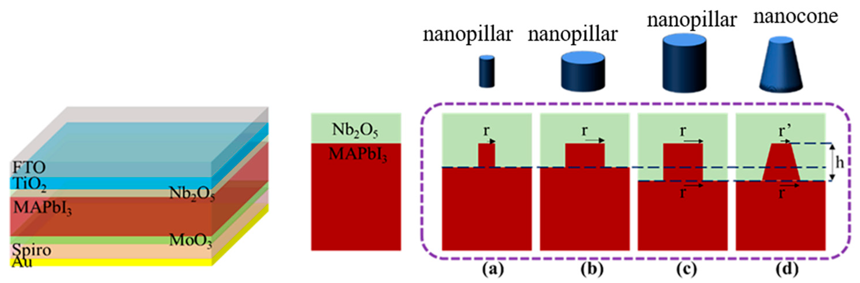
2.1. Design of PSCs Model

In this study, the standard device structure of the perovskite solar cell (PSCs) model is FTO/TiO2/CH3NH3PbI3/Spiro-OMeTAD/Au. In the optimized structure, molybdenum trioxide (MoO3) and niobium pentoxide (Nb2O5) are introduced as interfacial transition layers between the perovskite layer and HTL, and the transition layers between perovskite layer and ETL, respectively. The light source irradiating the solar cell is set as a vertically incident plane wave light source. The top and bottom are both scattering boundary conditions. The X-direction and Y-direction sides of the non-metallic layer are periodic boundary conditions, while the sides of the metallic layer are set as perfect electrical conductors [23,24,25]. The mesh size is predefined as fine. The solver is specified as a parametric scan with a step size of 1 from 300 nm to 800 nm. Accordingly, the structure of the multi-transmission layer device becomes FTO/TiO2/Nb2O5/CH3NH3PbI3/MoO3/Spiro-OMeTAD/Au. MoO3 is an inorganic compound semiconductor with an energy level (−5.3 to −2.3 eV) between CH3NH3PbI3 (−5.4 to −3.9 eV) and Spiro-OMeTAD (−5.2 to −2.2 eV) [26,27]. Nb2O5 is a high-transmittance semiconductor that can be used to make optical glasses, with an energy level (−4.02 to −7.43 eV) between CH3NH3PbI3 (−5.4 to −3.9 eV) and TiO2 (−4.1 to −7.3 eV) [28]. These two transition layers effectively form a stepwise energy level alignment at the interfaces, reducing interfacial energy barriers and facilitating smoother charge transfer. To further compensate for the optical losses, a light-trapping structure is incorporated into the optimized device, which enhances the average light absorption of the device [29,30].

2.2. Simulation of the Generation of Charge Carriers in PSCs

In the finite element analysis model, the AM1.5G solar spectrum is imported. Then, the corresponding energy flux density of each wavelength photon is expressed as ΦAM1.5 (Ephoton, λ). The incident light intensity is obtained by integrating it (Equation (1)). Equation (2) is the relation between the electric field intensity and the incident light intensity obtained from Maxwell’s equation [31,32,33]. Since the refractive index of air is 1, the simplified result is |E|2 = 2Ι/(cε0) [34].
I = λ m i n λ m a x Φ A M 1.5 d λ
Ι = c n ε 0 2 E 2
Combined with Poynting vector divergence, the absorbed power per unit volume of perovskite can be calculated using Equation (3). Assuming that the material is an isotropic homogeneous medium under ideal conditions, it is assumed that ε = ε0εr = 2ε0 nk. The total number of photogenerated carriers of perovskite materials can be obtained by Equations (4)–(6). In the equations, ε, ω and Ιm represent the dielectric constant, angular frequency, and the imaginary part of the complex refractive index of the material, respectively [35].
Ρ a b s = 1 2 ω E x , y , z , I 2 Ι m x , y , z , ω
g x , y , z , ω = Ρ a b s ω = ω 2 E x , y , z , ω 2 Ι m x , y , z , ω
g x , y , z , ω = ε 2 E x , y , z , ω 2
G x , y , z = g x , y , z , ω d ω

2.3. Simulation of Drift Diffusion Model

Device parameters and performance are calculated by numerically solving the fundamental semiconductor equations. The Poisson equation (Equation (7)) relates the electrostatic potential to the total charge density. The drift diffusion equations (Equations (8) and (9)) describe the motion of charge carriers in semiconductors. It is possible to calculate the potential distribution and carrier concentration distribution in the semiconductor combined with the Poisson equation [36]. Then, incorporate the continuity equations (Equations (10) and (11)) to describe the drift and diffusion motion of ions [37].
· ε φ = q ( n p N D + + N A )
J n = n q μ n φ + q D n n
J p = p q μ p φ + q D p p
n t = 1 q J n + G U
p t = 1 q J p + G U
In these equations, the symbols denote the following physical quantities: mobility (µ), current density (J), diffusion coefficients (D), electrostatic potential (φ), dielectric constant (ε), elementary charge (q), carrier generation rate (G), and recombination rate (U). For the electrical simulation, the absorption result of optical simulation is converted into the total number of carrier generations Gtotal as the input. The electrical characteristic curves of perovskite solar cell devices can be obtained by inputting the electrical property parameters corresponding to different materials into the established model.

3. Results and Analysis

3.1. Effects of Transition Layers

The structural diagram of a perovskite solar cell model is shown in Figure 1. The MoO3 transition layers exist between the perovskite layer and the HTL, and the Nb2O5 transition layers exist between the perovskite layer and the ETL. In order to investigate the precise impact of the transition layers on PSCs, we conducted numerical simulations to analyze the performance variations in devices without and with transition layers. The material property parameters required for numerical simulation are presented in Table 1 [38,39,40,41,42,43].
Figure 2a,b shows the current density–voltage (J-V) curves and power density–voltage curves of the devices with and without transition layers. The inset table of Figure 2a shows the corresponding electrical performance parameters. These results show that the open-circuit voltage (VOC) of the device increased from 0.98 V to 1.03 V when MoO3 material was used as HTL, and the PCE increased from 15.05% to 17.06%. In addition, while the Nb2O5 material was intercalated as an ETL, the VOC of the device was further increased from 1.03 V to 1.06 V, and the PCE increased to 17.33%. The increased VOC is attributed to the disparity position between the conduction band and valence band between the semiconductor materials. The band alignment affects the extraction of electrons and holes during the formation of a semiconductor PN junction. When the solar cells work, the electrons excited to conduct electricity drift towards the cathode under the action of the built-in electric field, and the holes left behind move towards the anode in the same way. The ability of charge extraction can be enhanced if the material forms stepped energy levels [44,45]. Moreover, the FF increases from 79.74% to 82.53% when MoO3 and Nb2O5 transition layers are introduced. According to previous reports, energy level alignment facilitates the reduction in carrier recombination, thereby enhancing the FF performance of the device [46]. The internal energy level diagram of the PSC device is shown in Figure 3.
The suitability of MoO3 as a transition layer between CH3NH3PbI3 and Spiro-OMeTAD stems from its role in creating a cascaded valence band alignment across these materials. As shown in Figure 3, the conduction band minimum of MoO3 is higher than CH3NH3PbI3, which can block the transfer of electrons to the anode. Similarly, the conduction band minimum of Nb2O5 is located between the CH3NH3PbI3 and TiO2, which can enhance the efficiency of electron extraction when utilized as a transition layer for electron transport. The lower energy level difference in the valence band maximum can also effectively inhibit electron–hole recombination [47,48]. These band alignment designs supply ascending VOC, resulting in superior PCE.

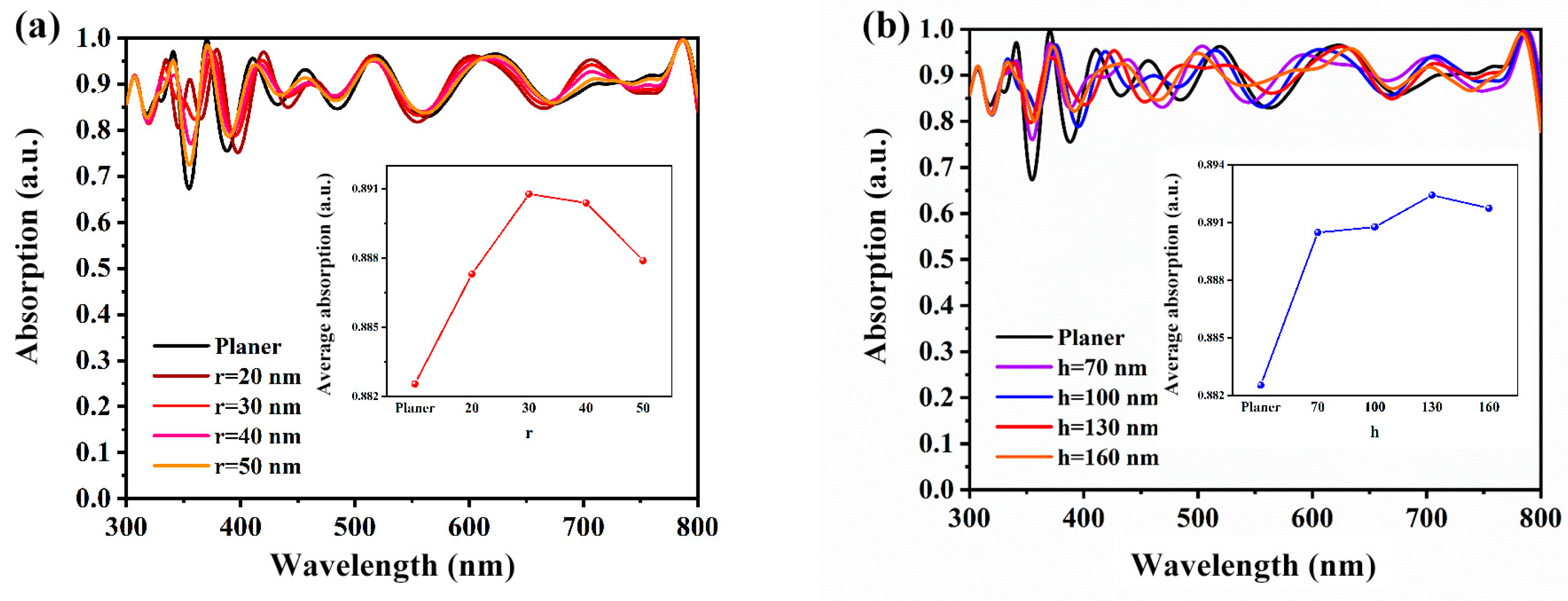
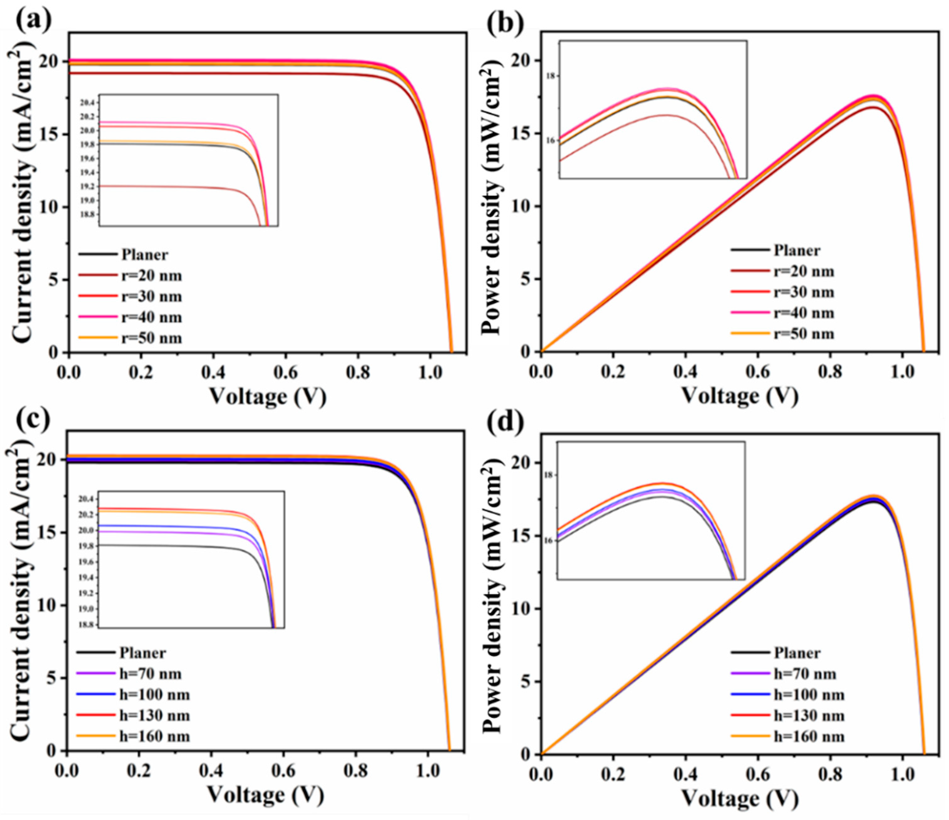
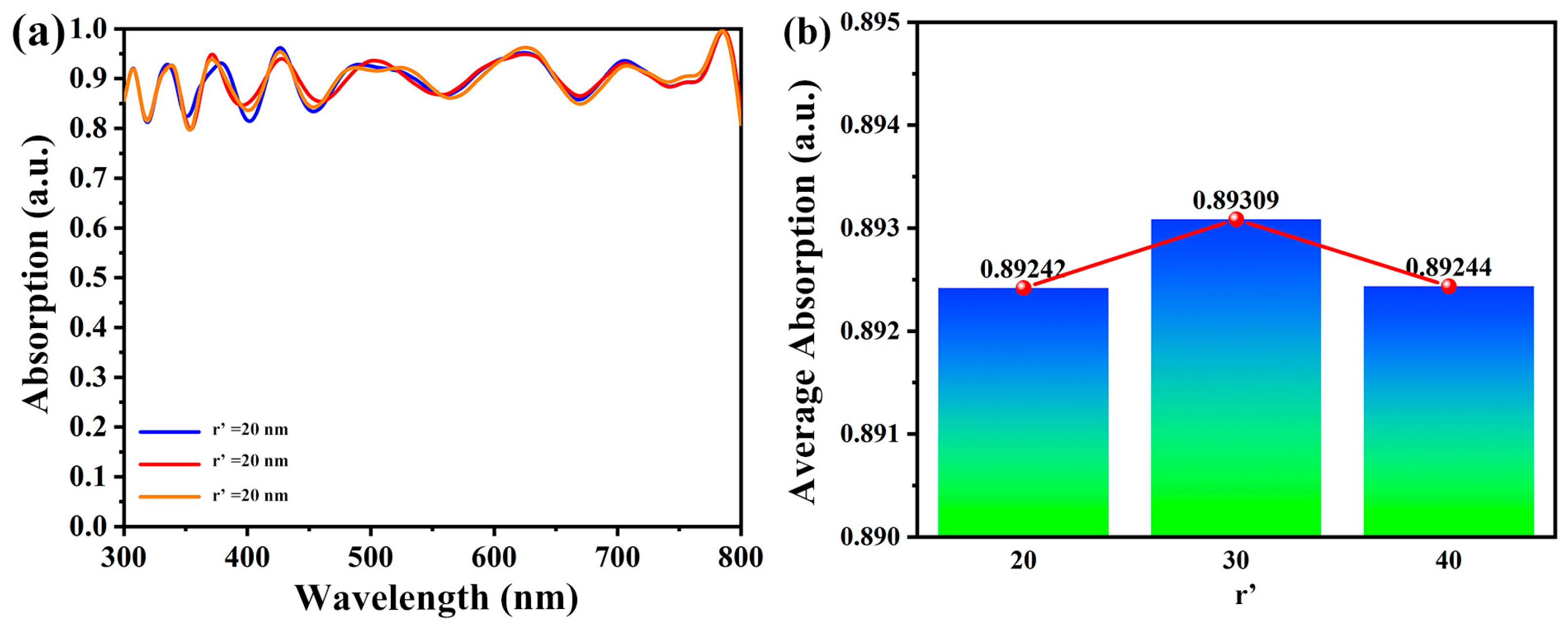
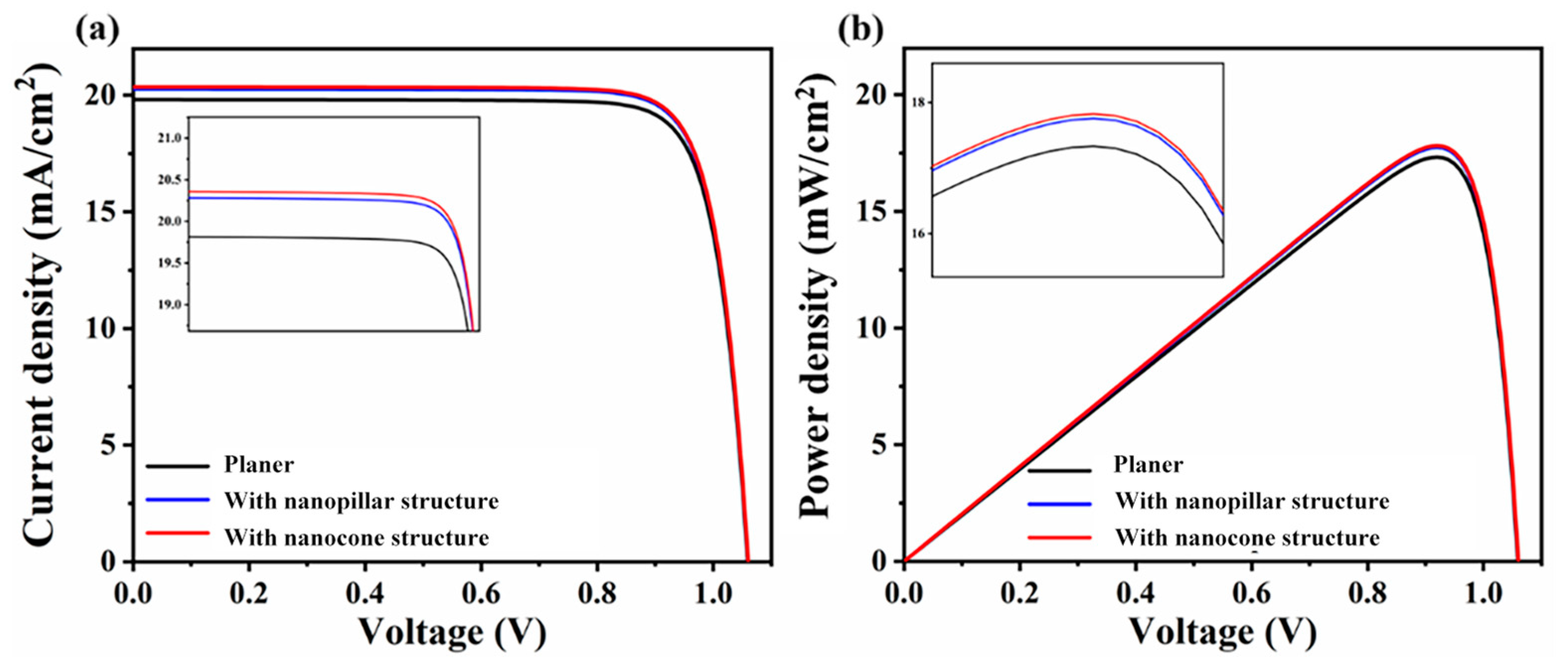
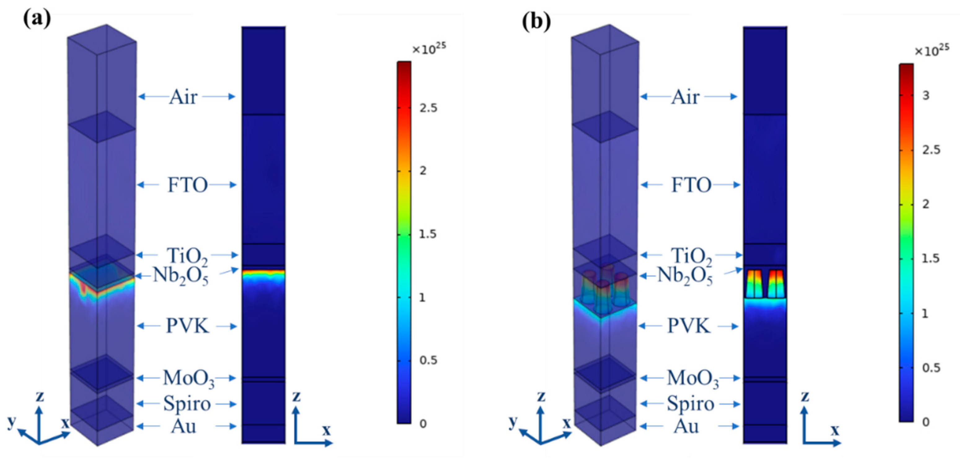
3.2. Effects of Light-Trapping Structure

When introducing Nb2O5 as a transition layer, the short-circuit current density (JSC) decreases. This is due to the overall transmittance decreasing, which stems from the lower transmittance of Nb2O5 than FTO and TiO2 in the wavelength band of 400 nm to 600 nm (Figure 4a,b), resulting in reduced photon energy reaching the perovskite active layer.
In order to mitigate optical losses within the device, we designed a light-trapping structure at the interface. This structure extends the optical path of incident light through multiple reflections, thereby reducing transmittance and enhancing absorption. The optical process is illustrated the four stages, as shown in Figure 5. We first investigated the optimization of the optical properties of the device with different radii (r), and the height (h) of the nanopillar perovskite structures was fixed at 100 nm. As shown in Figure 6a, by comparing the absorption curves of structural devices with radii r of 20 nm, 30 nm, 40 nm and 50 nm, it was found that the absorption of wavelength bands from 340 nm to 360 nm and 600 nm to 780 nm obviously change with the gradual increase in array radius. The phenomenon between 600 nm and 780 nm is due to the influence of perovskite materials. When the radius is small, the space between the structures is large, and the gap between the structures decreases as the radius gradually increases [49,50,51]. The modeled structure we designed consists of perovskite cylinders with voids filled by Nb2O5. When the radius of the cylinder is small, the content of Nb2O5 increases relative to that of the plane type. The absorption in the 340 nm to 360 nm band is enhanced because Nb2O5 is a wide-bandgap semiconductor. As the radius of the cylinder increases, the volume of Nb2O5 decreases, so the absorption here decreases. To evaluate the overall absorption enhancement, we computed the average absorption across the spectrum (Figure 6a). The device achieves the highest average absorption of 89.08% at a radius of r = 30 nm.
After determining the optimal radius parameters, we adjusted its height, and the absorption results are shown in Figure 6b. In the band from 340 nm to 360 nm, the absorption gradually increased with the increasing height of the nanopillar structure. This was caused by the gradual increase in the volume of Nb2O5, which aligns with the behavior observed when the radius was optimized. The change in the 600 nm to 780 nm band comes from the change in the volume of the perovskite material, and increasing height leads to a reduction in the thickness of the intact perovskite film, causing the absorption to gradually decrease [52,53,54]. By comparing the average absorption rate, it is shown that the optimal absorption rate of the device is 89.24% at h = 130 nm.
Figure 7a,b describe the contact between short-circuit current density, power density, and the radius of the cylinder, respectively. The maximum short-circuit current density of the device is 20.12 mA/cm2 when the radius r is 40 nm, which is inconsistent with the result of the optical absorption rate. We speculate that due to the content of Nb2O5 at 40 nm of r being less than that at 30 nm, the absorption enhancement of the device is partly due to the absorption contribution of Nb2O5, which is not fully absorbed and utilized by the perovskite active layer. The maximum power density is 17.61 mW/cm2 when the radius is 40 nm. When the radius increases to 50 nm, the light-trapping capacity is affected by the smaller trapping space, resulting in a decrease in efficiency [55,56,57]. The corresponding specific device parameters are shown in Table 2.
The height parameters of the structure are carried out after determining the value interval of the radius (40 nm). With the increase in the height of the cylinder in the nanopillar-aligned nanopillar structure device, the short-circuit current density of the device first increases and then decreases, as shown in Figure 7c. This is owed to the enhanced light absorption capacity of the device with the help of the nanopillar-aligned nanopillar structure, which assists the perovskite layer in obtaining more photon energy, resulting in increasing JSC. In the process of increasing the height, the light-trapping effect is gradually enhanced, and the short-circuit current density increases with the increase in the light absorption rate [58,59]. The specific parameters of the device are shown in Table 2. It is interesting that there exists a critical value while the height reaches 130 nm. If h continues to increase, the volume of the perovskite active layer will be excessively compressed, so that the short-circuit current density will begin to decline. The corresponding power results are shown in Figure 7d. When the height reaches 130 nm, the maximum power density reaches 17.76 mW/cm2.
In order to further explore the effect of optical structure on device performance, we fine-tuned the nanopillar-aligned nanopillar structure. In the process of parameter optimization, we concluded that the optimal absorption effect can be obtained when the radius is between 20 nm and 40 nm. Therefore, we fixed the height within this parameter interval as 130 nm, and the bottom radius as 40 nm. We transformed the nanocone structure into a nanopillar structure by reducing the top radius r’. The optical absorption curves are shown in Figure 8a. As the top radius of the nanocone r’ decreased, the average light absorption of the device climbed up and then declined. In Figure 8b, the average light absorption rate reached 89.31% when r’ = 30 nm, which is even higher than the average light absorption rate of the optimized nanocone device. This result was due to the tilted sides of the nanopillar structure, which could achieve multi-angle light reflection [60,61,62]. By comparing the planar, nanopillar, and nanocone devices, it was found that the efficiency of the nanopillar device was the highest, reaching 17.83%. The resulting electrical curves are shown in Figure 9 and the complete data are shown in Table 2.
To verify that the nanocone structure enhances light utilization, we simulated and monitored the carrier generation process of the perovskite layer, as shown in Figure 10. When vertically incident AM 1.5G sunlight irradiated the device from above, the light was rapidly absorbed on the surface of the perovskite due to the high optical absorption coefficient of the perovskite, and the device realized the process of converting photon energy into photogenic excitons [63,64,65,66]. The simulation results demonstrate that the existence of the nanocone structure can improve the carrier generation rate of the device when it is irradiated by sunlight [67,68,69]. This improvement arises from the optical trapping effect of the nanocone array causing the surface of the active layer to absorb more light, which is consistent with the increase in the short-circuit current density in the J-V curve. The structure greatly improves the specific surface area of the perovskite active layer and increases the contact area with the electron transport layer [70,71,72]. We hypothesize that this structured interface optimizes electron transport and extraction efficiency.

4. Conclusions

Utilizing finite element analysis, this study investigates dual-transition layers (MoO3/Nb2O5) coupled with light-trapping nanostructures to enhance perovskite solar cell (PSC) performance. The introduction of transition layers establishes graded energy level alignments at semiconductor interfaces, which can optimize carrier extraction and increase the open-circuit voltage of the device. The performance of the device can be optimized from both optical and electrical aspects by combining it with the light-trapping structure, which can enhance optical absorption. As a result, the simulation results show that the open-circuit voltage of perovskite solar cells increases from 0.98V to 1.06V when transition layers (MoO3, Nb2O5) are introduced. Compared with the planar intercalated device without an optical trap structure, the one with perovskite nanocone arrays has an average light absorption rate of 89.31%, and the carrier generation rate is improved. The short-circuit current density of the optimal parameter model reaches 20.36 mA/cm2, and the photoelectric conversion efficiency is 17.83%, which increases by 18.47% compared with the initial device. These findings provide critical design guidelines for next-generation perovskite photovoltaics. The graded band alignment strategy using MoO3/Nb2O5 dual-transition layers offers a reproducible approach to minimize interfacial recombination in industrial-scale manufacturing, while light-trapping nanopillar arrays demonstrate scalable photon management potential for roll-to-roll production. The Nb2O5/MoO3 interfacial architecture shows particular promise for tandem cell integration due to its spectral tuning capabilities.

Author Contributions

Conceptualization and data curation: L.L., W.L., Q.L. and Z.Y.; formal analysis: L.L., W.L. and Q.L.; methodology: L.L., W.L., Q.L., Y.C., X.Y. and Y.Z.; resources: L.L., Z.Y. and Y.Z.; software: Y.C., X.Y., Y.Z. and Z.Y.; writing—original draft preparation: L.L. and W.L.; writing—review and editing: L.L., W.L., Q.L. and Z.Y. All authors have read and agreed to the published version of the manuscript.

Funding

The project is supported by Sichuan Science and Technology Program (2024ZDZX0030).

Institutional Review Board Statement

Not applicable.

Informed Consent Statement

Not applicable.

Data Availability Statement

The data are contained within the article.

Conflicts of Interest

The authors declare no conflicts of interest.

References

  1. Liu, G.; Dai, Y.; Sun, X.; Ma, J.; Xian, T.; Yang, H. Synergistically regulating energy band structure and forming quantum wells to enhance the photocatalytic activity of Bi2MoO6 for tetracycline removal. Sep. Purif. Technol. 2025, 361, 131622. [Google Scholar] [CrossRef]
  2. Ren, J.; Ma, Q.; Sun, X.; Ma, J.; Liu, G.; Yang, H. In3+-doping and oxygen vacancies co-engineering active sites of Bi2WO6 hollow nanospheres to achieve efficient photoreduction of CO2 to CO with nearly 100% selectivity. Fuel 2025, 397, 135454. [Google Scholar] [CrossRef]
  3. Ren, J.; Ma, Q.; Sun, X.; Wang, S.; Liu, G.; Yang, H. Interface-engineering enhanced photocatalytic conversion of CO2 into solar fuels over S-type Co-Bi2WO6@Ce-MOF heterostructured photocatalysts. J. Colloid Interface Sci. 2025, 691, 137452. [Google Scholar] [CrossRef] [PubMed]
  4. Xiao, T.; Tu, S.; Liang, S.; Guo, R.; Tian, T.; Müller-Buschbaum, P. Solar cell-based hybrid energy harvesters towards sustainability. Opto-Electron. Sci. 2023, 2, 230011. [Google Scholar] [CrossRef]
  5. Liu, S.; Li, J.; Xiao, W.; Chen, R.; Sun, Z.; Zhang, Y.; Lei, X.; Hu, S.; Kober-Czerny, M.; Wang, J.; et al. Buried interface molecular hybrid for inverted perovskite solar cells. Nature 2024, 632, 536–542. [Google Scholar] [CrossRef] [PubMed]
  6. Liu, Y.; Liu, M.; Yang, H.; Yi, Z.; Zhang, H.; Tang, C.; Deng, J.; Wang, J.; Li, B. Photoelectric simulation of perovskite solar cells based on two inverted pyramid structures. Phys. Lett. A 2025, 552, 130653. [Google Scholar] [CrossRef]
  7. Yan, X.F.; Lin, Q.; Wang, L.-L.; Liu, G.-D. Tunable strong plasmon–exciton coupling based modulator employing borophene and deep subwavelength perovskite grating. J. Phys. D Appl. Phys. 2023, 56, 435106. [Google Scholar] [CrossRef]
  8. Meyer, E.L.; Jakalase, S.; Nqombolo, A.; Rono, N.; Agoro, M.A. The Numerical Simulation of a Non-Fullerene Thin-Film Organic Solar Cell with Cu2FeSnS4(CFTS) Kesterite as a Hole Transport Layer Using SCAPS-1D. Coatings 2025, 15, 266. [Google Scholar] [CrossRef]
  9. Ma, Q.; Ren, J.; Sun, X.; Wang, S.; Chen, X.; Liu, G.; Yang, H. Enhanced CO2 photoreduction over S-scheme Sdoped-BiVO4/AgCl heterostructures and interface interaction mediated selective generation of CH4. Chem. Eng. J. 2025, 509, 161444. [Google Scholar] [CrossRef]
  10. Chen, D.; Xie, Y.; Chen, T.; Zhang, T.; Huang, Y.; Qiu, X. Low-temperature water-processed NiO hole transport layers for high-efficiency CH3NH3PbI3 perovskite solar cells. Opt. Mater. 2024, 149, 114997. [Google Scholar] [CrossRef]
  11. Chen, Q.; Asgarimoghaddam, H.; Ji, W.; Wu, W.; Cao, J.; Wang, R.; Yu, W.; Nie, X.; Zhou, Y.; Song, B.; et al. CuS nanosheets as additives in the hole transport layers for stable p-i-n perovskite solar cells. Nano Energy 2025, 135, 110652. [Google Scholar] [CrossRef]
  12. Ansari, F.; Zheng, L.; Pfeifer, L.; Eickemeyer, F.T.; Zakeeruddin, S.M.; Lempesis, N.; Carnevali, V.; Vezzosi, A.; Sláma, V.; Georges, T.; et al. Dopamine Dopes the Performance of Perovskite Solar Cells. Adv. Mater. 2025, e2501075. [Google Scholar] [CrossRef] [PubMed]
  13. Yang, J.; Li, X.; Gu, J.; Yu, F.; Chen, J.; Lu, W.; Chen, X. High-Stability WSe2 Homojunction Photodetectors via Asymmetric Schottky and PIN Architectures. Coatings 2025, 15, 301. [Google Scholar] [CrossRef]
  14. Duan, L.; Liu, S.; Wang, X.; Zhang, Z.; Luo, J. Interfacial Crosslinking for Efficient and Stable Planar TiO2 Perovskite Solar Cells. Adv. Sci. 2024, 11, e2402796. [Google Scholar] [CrossRef] [PubMed]
  15. Chen, L.; Luo, W.; Fang, B.; Zhu, B.; Zhang, W. Study on light absorption of CH3NH3PbI3 perovskite solar cells enhanced by gold nanobipyramids. Opt. Laser Technol. 2022, 159, 108924. [Google Scholar] [CrossRef]
  16. Tiwari, P.; Alotaibi, M.F.; Al-Hadeethi, Y.; Srivastava, V.; Arkook, B.; Sadanand; Lohia, P.; Dwivedi, D.K.; Umar, A.; Algadi, H.; et al. Design and Simulation of Efficient SnS-Based Solar Cell Using Spiro-OMeTAD as Hole Transport Layer. Nanomaterials 2022, 12, 2506. [Google Scholar] [CrossRef] [PubMed]
  17. Li, C.; Xu, F.; Li, Y.; Li, N.; Yu, H.; Yuanb, B.; Chen, Z.; Li, L.; Cao, B. An ultrahigh 84.3% fill factor for efficient CH3NH3PbI3 P-i-N perovskite film solar cell. Sol. Energy 2022, 233, 271–277. [Google Scholar] [CrossRef]
  18. Sun, X.; Zhang, J.; Ma, J.; Xian, T.; Liu, G.; Yang, H. Synthesis of strongly interactive FeWO4/BiOCl heterostructures for efficient photoreduction of CO2 and piezo-photodegradation of bisphenol A. Chem. Eng. J. 2024, 496, 153961. [Google Scholar] [CrossRef]
  19. Tesfancheal, H.Y.; Wang, Z.; Chen, J.; Wang, M.; Li, Z.; Pan, J.; Li, X.; Cai, M. Multi-physics device simulations of optimized semi-transparent perovskite solar cells: Influence of material types and layer thicknesses on transmittance and electrical performance. Sol. Energy 2024, 284, 113069. [Google Scholar] [CrossRef]
  20. Gu, X.; Liu, X.; Yan, X.-F.; Du, W.-J.; Lin, Q.; Wang, L.-L.; Liu, G.-D. Polaritonic coherent perfect absorption based on self-hybridization of a quasi-bound state in the continuum and exciton. Opt. Express 2023, 31, 4691–4700. [Google Scholar] [CrossRef] [PubMed]
  21. Khatoon, S.; Chakraborty, V.; Yadav, S.K.; Diwakar, S.; Singh, J.; Singh, R.B. Simulation study of CsPbIxBr1-x and MAPbI3 heterojunction solar cell using SCAPS-1D. Sol. Energy 2023, 254, 137–157. [Google Scholar] [CrossRef]
  22. Xiao, Y.; Ma, C.; Sun, T.; Song, Q.; Bian, L.; Yi, Z.; Hao, Z.; Tang, C.; Wu, P.; Zeng, Q. Investigation of a high-performance solar absorber and thermal emitter based on Ti and InAs. J. Mater. Chem. A 2024, 12, 29145–29151. [Google Scholar] [CrossRef]
  23. Ai, Z.; Yang, H.; Liu, M.; Cheng, S.; Wang, J.; Tang, C.; Gao, F.; Li, B. Phase-transition-enabled dual-band camouflage in VO2/Ag multilayered nanostructures. Phys. E Low-Dimens. Syst. Nanostructures 2025, 173, 116327. [Google Scholar] [CrossRef]
  24. Liu, H.; Li, J.; Yang, H.; Wang, J.; Li, B.; Zhang, H.; Yi, Y. TiN-Only Metasurface Absorber for Solar Energy Harvesting. Photonics 2025, 12, 443. [Google Scholar] [CrossRef]
  25. Yang, C.; Luo, M.; Ju, X.; Hu, J. Ultra-narrow dual-band perfect absorber based on double-slotted silicon nanodisk arrays. J. Phys. D Appl. Phys. 2024, 57, 345104. [Google Scholar] [CrossRef]
  26. Seo, S.; Akino, K.; Nam, J.; Shawky, A.; Lin, H.; Nagaya, H.; Kauppinen, E.I.; Xiang, R.; Matsuo, Y.; Jeon, I.; et al. Multi-Functional MoO3 Doping of Carbon-Nanotube Top Electrodes for Highly Transparent and Efficient Semi-Transparent Perovskite Solar Cells. Adv. Mater. Interfaces 2022, 9, 2101595. [Google Scholar] [CrossRef]
  27. Hanmandlu, C.; Chen, C.-Y.; Boopathi, K.M.; Lin, H.-W.; Lai, C.-S.; Chu, C.-W. Bifacial Perovskite Solar Cells Featuring Semitransparent Electrodes. ACS Appl. Mater. Interfaces 2017, 9, 32635–32642. [Google Scholar] [CrossRef] [PubMed]
  28. Gu, B.; Zhu, Y.; Lu, H.; Tian, W.; Li, L. Efficient planar perovskite solar cells based on low-cost spin-coated ultrathin Nb2O5 films. Sol. Energy 2018, 166, 187–194. [Google Scholar] [CrossRef]
  29. Xiang, T.; Sun, Z.; Wang, L.-L.; Lin, Q.; Liu, G.-D. Polarization independent perfect absorption of borophene metamaterials operating in the communication band. Phys. Scr. 2024, 99, 085519. [Google Scholar] [CrossRef]
  30. Chen, Z.; Cheng, S.; Zhang, H.; Yi, Z.; Tang, B.; Chen, J.; Zhang, J.; Tang, C. Ultra wideband absorption absorber based on Dirac semimetallic and graphene metamaterials. Phys. Lett. A 2024, 517, 129675. [Google Scholar] [CrossRef]
  31. Balashov, I.S.; Chezhegov, A.A.; Chizhov, A.S.; Grunin, A.A.; Anokhin, K.V.; Fedyanin, A.A. Light-stimulated adaptive artificial synapse based on nanocrystalline metal-oxide film. Opto-Electron. Sci. 2023, 2, 230016. [Google Scholar] [CrossRef]
  32. Luo, H.; Zhu, Y.; Song, Q.; Yi, Y.; Yi, Z.; Zeng, Q.; Li, Z. Ultra-High-Efficiency Solar Capture Device Based on InAs Top Microstructure. Coatings 2024, 14, 1297. [Google Scholar] [CrossRef]
  33. Hu, J.; Tan, C.; Bai, W.; Li, Y.; Lin, Q.; Wang, L.-L. Dielectric nanocavity-coupled surface lattice resonances for high-efficiency plasmonic sensing. J. Phys. D Appl. Phys. 2021, 55, 075105. [Google Scholar] [CrossRef]
  34. Gu, N.; Chen, H.; Tang, A.; Fan, X.; Noda, C.Q.; Xiao, Y.; Zhong, L.; Wu, X.; Zhang, Z.; Yang, Y.; et al. Embedded solar adaptive optics telescope: Achieving compact integration for high-efficiency solar observations. Opto-Electron. Adv. 2025, 8, 250025. [Google Scholar] [CrossRef]
  35. Yan, D.; Tang, C.; Yi, Z.; Wang, J.; Li, B. A fully symmetric solar absorber for thermophotovoltaic power generation. Phys. Lett. A 2025, 542, 130461. [Google Scholar] [CrossRef]
  36. Zhang, F.; Camarero, P.; Haro-González, P.; Labrador-Páez, L.; Jaque, D. Optical trapping of optical nanoparticles: Fundamentals and applications. Opto-Electron. Sci. 2023, 2, 230019. [Google Scholar] [CrossRef]
  37. Ren, X.; Wang, Z.; Sha, W.E.I.; Choy, W.C.H. Exploring the Way To Approach the Efficiency Limit of Perovskite Solar Cells by Drift-Diffusion Model. ACS Photon. 2017, 4, 934–942. [Google Scholar] [CrossRef]
  38. Shen, H.; Jacobs, D.A.; Wu, Y.; Duong, T.; Peng, J.; Wen, X.; Fu, X.; Karuturi, S.K.; White, T.P.; Weber, K.; et al. Inverted Hysteresis in CH3NH3PbI3 Solar Cells: Role of Stoichiometry and Band Alignment. J. Phys. Chem. Lett. 2017, 8, 2672–2680. [Google Scholar] [CrossRef] [PubMed]
  39. Otoufi, M.K.; Ranjbar, M.; Kermanpur, A.; Taghavinia, N.; Minbashi, M.; Forouzandeh, M.; Ebadi, F. Enhanced performance of planar perovskite solar cells using TiO2/SnO2 and TiO2/WO3 bilayer structures: Roles of the interfacial layers. Sol. Energy 2020, 208, 697–707. [Google Scholar] [CrossRef]
  40. Courtier, N.E.; Cave, J.M.; Foster, J.M.; Walker, A.B.; Richardson, G. How transport layer properties affect perovskite solar cell performance: Insights from a coupled charge transport/ion migration model. Energy Environ. Sci. 2019, 12, 396–409. [Google Scholar] [CrossRef]
  41. Almora, O.; Lopez-Varo, P.; Cho, K.T.; Aghazada, S.; Meng, W.; Hou, Y.; Echeverría-Arrondo, C.; Zimmermann, I.; Matt, G.J.; Jiménez-Tejada, J.A.; et al. Ionic dipolar switching hinders charge collection in perovskite solar cells with normal and inverted hysteresis. Sol. Energy Mater. Sol. Cells 2019, 195, 291–298. [Google Scholar] [CrossRef]
  42. Bitton, S.; Tessler, N. Electron/hole blocking layers as ionic blocking layers in perovskite solar cells. J. Mater. Chem. C 2021, 9, 1888–1894. [Google Scholar] [CrossRef]
  43. Xiang, J.; Li, Y.; Huang, F.; Zhong, D. Effect of interfacial recombination, bulk recombination and carrier mobility on the JV hysteresis behaviors of perovskite solar cells: A drift-diffusion simulation study. Phys. Chem. Chem. Phys. 2019, 21, 17836–17845. [Google Scholar] [CrossRef] [PubMed]
  44. Li, W.; Cheng, S.; Yi, Z.; Zhang, H.; Song, Q.; Hao, Z.; Sun, T.; Wu, P.; Zeng, Q.; Raza, R. Advanced optical reinforcement materials based on three-dimensional four-way weaving structure and metasurface technology. Appl. Phys. Lett. 2025, 126, 033503. [Google Scholar] [CrossRef]
  45. Luo, M.; Hu, J.; Li, Y.; Bai, W.; Zhang, R.; Lin, Q.; Wang, L.-L. Anapole-assisted ultra-narrow-band lattice resonance in slotted silicon nanodisk arrays. J. Phys. D Appl. Phys. 2023, 56, 375102. [Google Scholar] [CrossRef]
  46. Zhang, C.; Liang, S.; Liu, W.; Eickemeyer, F.T.; Cai, X.; Zhou, K.; Bian, J.; Zhu, H.; Zhu, C.; Wang, N.; et al. Ti1–graphene single-atom material for improved energy level alignment in perovskite solar cells. Nat. Energy 2021, 6, 1154–1163. [Google Scholar] [CrossRef]
  47. Sun, X.F.; Xian, T.; Sun, C.Y.; Zhang, J.Q.; Liu, G.R.; Yang, H. Enhancing CO2 photoreduction on Au@CdZnS@MnO2 hollow nanospheres via electron configuration modulation. J. Mater. Sci. Technol. 2025, 228, 256–268. [Google Scholar] [CrossRef]
  48. Wang, H.-Y.; Ma, R.; Liu, G.-D.; Wang, L.-L.; Lin, Q. Optical force conversion and conveyor belt effect with coupled graphene plasmon waveguide modes. Opt. Express 2023, 31, 32422–32433. [Google Scholar] [CrossRef] [PubMed]
  49. Cheng, S.; Li, W.; Zhang, H.; Akhtar, M.N.; Yi, Z.; Zeng, Q.; Ma, C.; Sun, T.; Wu, P.; Ahmad, S. High sensitivity five band tunable metamaterial absorption device based on block like Dirac semimetals. Opt. Commun. 2024, 569, 130816. [Google Scholar] [CrossRef]
  50. Li, B.; Liu, M.; Wen, R.; Wei, Y.; Zeng, L.; Deng, C.-S. Dynamic control of Fano-like interference in the graphene periodic structure. J. Phys. D Appl. Phys. 2023, 56, 115104. [Google Scholar] [CrossRef]
  51. Hu, J.; Bai, W.; Tan, C.; Li, Y.; Lin, Q.; Wang, L. Highly electric field enhancement induced by anapole modes coupling in the hybrid dielectric–metal nanoantenna. Opt. Commun. 2022, 511, 127987. [Google Scholar] [CrossRef]
  52. Li, Z.-T.; Li, X.; Liu, G.-D.; Wang, L.-L.; Lin, Q. Analytical investigation of unidirectional reflectionless phenomenon near the exceptional points in graphene plasmonic system. Opt. Express 2023, 31, 30458–30468. [Google Scholar] [CrossRef] [PubMed]
  53. Mu, W.; Xu, M.; Sun, X.; Liu, G.; Yang, H. Oxygen-vacancy-tunable mesocrystalline ZnO twin “cakes” heterostructured with CdS and Cu nanoparticles for efficiently photodegrading sulfamethoxazole. J. Environ. Chem. Eng. 2024, 12, 112367. [Google Scholar] [CrossRef]
  54. Zeng, Z.; Liu, H.; Zhang, H.; Cheng, S.; Yi, Y.; Yi, Z.; Wang, J.; Zhang, J. Tunable ultra-sensitive four-band terahertz sensors based on Dirac semimetals. Photon-Nanostructures Fundam. Appl. 2024, 63, 101347. [Google Scholar] [CrossRef]
  55. Zhang, B.; Luo, Y. Dynamic optical tuning and sensing in L-shaped dirac semimetal-based terahertz metasurfaces. Phys. Lett. A 2025, 541, 130419. [Google Scholar] [CrossRef]
  56. Li, W.; Cheng, S.; Zhang, H.; Yi, Z.; Tang, B.; Ma, C.; Wu, P.; Zeng, Q.; Raza, R. Multi-functional metasurface: Ultra-wideband/multi-band absorption switching by adjusting guided-mode resonance and local surface plasmon resonance effects. Commun. Theor. Phys. 2024, 76, 065701. [Google Scholar] [CrossRef]
  57. Li, Y.; Tan, C.; Hu, J.; Bai, W.; Zhang, R.; Lin, Q.; Zhang, Y.; Wang, L. Ultra-narrow band perfect absorbance induced by magnetic lattice resonances in dielectric dimer metamaterials. Results Phys. 2022, 39, 105730. [Google Scholar] [CrossRef]
  58. Li, Y.; Huang, X.; Liu, S.; Liang, H.; Ling, Y.; Su, Y. Metasurfaces for near-eye display applications. Opto-Electron. Sci. 2023, 2, 230025. [Google Scholar] [CrossRef]
  59. Ai, Z.; Liu, H.; Cheng, S.; Zhang, H.; Yi, Z.; Zeng, Q.; Wu, P.; Zhang, J.; Tang, C.; Hao, Z. Four peak and high angle tilted insensitive surface plasmon resonance graphene absorber based on circular etching square window. J. Phys. D Appl. Phys. 2025, 58, 185305. [Google Scholar] [CrossRef]
  60. Liu, M.; Li, B.; Zeng, L.; Wei, Y.; Wen, R.; Zhang, X.; Deng, C. Dynamic tunable narrow-band perfect absorber for fiber -optic communication band based on liquid crystal. J. Phys. D Appl. Phys. 2023, 56, 505102. [Google Scholar] [CrossRef]
  61. Zhang, J.; Sun, X.; Zhu, W.; Liu, G.; Xian, T.; Yang, H. Design of CdZnS/BiOCl heterostructure as a highly-efficient piezo-photocatalyst for removal of antibiotic. J. Environ. Chem. Eng. 2024, 12, 114405. [Google Scholar] [CrossRef]
  62. Li, W.; Yi, Y.; Yang, H.; Cheng, S.; Yang, W.; Zhang, H.; Yi, Z.; Yi, Y.; Li, H. Active tunable terahertz bandwidth absorber based on single layer graphene. Commun. Theor. Phys. 2023, 75, 045503. [Google Scholar] [CrossRef]
  63. Ma, R.; Zhang, L.-G.; Zeng, Y.; Liu, G.-D.; Wang, L.-L.; Lin, Q. Extreme enhancement of optical force via the acoustic graphene plasmon mode. Opt. Express 2023, 31, 6623–6632. [Google Scholar] [CrossRef] [PubMed]
  64. Li, Z.; Cheng, S.; Zhang, H.; Yang, W.; Yi, Z.; Yi, Y.; Wang, J.; Ahmad, S.; Raza, R. Ultrathin broadband terahertz metamaterial based on single-layer nested patterned graphene. Phys. Lett. A 2025, 534, 130262. [Google Scholar] [CrossRef]
  65. Wang, X.Y.; Lin, Q.; Wang, L.-L.; Liu, G.-D. Dynamic control of polarization conversion based on borophene nanostructures in optical communication bands. Phys. Scr. 2024, 99, 085531. [Google Scholar] [CrossRef]
  66. Ling, Z.X.; Zeng, Y.; Liu, G.-D.; Wang, L.-L.; Lin, Q. Unified model for plasmon-induced transparency with direct and indirect coupling in borophene-integrated metamaterials. Opt. Express 2022, 30, 21966–21976. [Google Scholar] [CrossRef] [PubMed]
  67. Sun, X.; Zhang, J.; Luo, M.; Ma, J.; Xian, T.; Liu, G.; Yang, H. Elevating photocatalytic H2 evolution over ZnIn2S4@Au@Cd0.7Zn0.3S multilayer nanotubes via Au-mediating H–S antibonding-orbital occupancy. Chem. Eng. J. 2024, 499, 156455. [Google Scholar] [CrossRef]
  68. Zeng, T.Y.; Liu, G.-D.; Wang, L.-L.; Lin, Q. Light-matter interactions enhanced by quasi-bound states in the continuum in a graphene-dielectric metasurface. Opt. Express 2021, 29, 40177–40186. [Google Scholar] [CrossRef] [PubMed]
  69. Zeng, Y.; Ling, Z.-X.; Liu, G.-D.; Wang, L.-L.; Lin, Q. Tunable plasmonically induced transparency with giant group delay in gain-assisted graphene metamaterials. Opt. Express 2022, 30, 14103–14111. [Google Scholar] [CrossRef] [PubMed]
  70. Ma, Q.; Ren, J.; Sun, X.; Chen, X.; Liu, G.; Wang, S.; Yang, H. Strong evidence for interface-field-induced photocarrier separation in new AgFeO2-BiVO4 heterostructures and their efficient photo-Fenton degradation of ciprofoxacin. Appl. Surf. Sci. 2024, 679, 161275. [Google Scholar] [CrossRef]
  71. Wang, J.; Yang, J.; Mei, Y. Non-radiating anapole state in dielectric nanostructures and metamaterials. J. Phys. D Appl. Phys. 2025, 58, 203001. [Google Scholar] [CrossRef]
  72. Zhang, P.; Mi, X.; Lu, Q.-L.; Li, X.; Li, Y.; Ke, H.; Xiong, J. Poly[nitrilo(diphenoxyphosphoranylidyne)] passivated MAPbI3 film achieves 21.36% efficiency and superior multivariate stability for air-processed perovskite solar cells. Chem. Eng. J. 2024, 503, 158411. [Google Scholar] [CrossRef]
Figure 1. Perovskite solar cell model structure diagram: (a) standard; (b) with MoO3 transition layer between the perovskite layer and the HTL; (c) with MoO3 and Nb2O5 transition layer (between the perovskite layer and the ETL).
Coatings 15 00856 g001
Figure 2. (a) J-V curves; (b) corresponding power density–voltage curves of perovskite solar cells with and without transition layers.
Coatings 15 00856 g002
Figure 3. Energy level diagram of PSC device.
Coatings 15 00856 g003
Figure 4. (a) The transmittance curves of FTO, Nb2O5, and TiO2, respectively; (b) the overall transmittance curves of the material superimposed with the structure of FTO-TiO2 and FTO-TiO2-Nb2O5.
Coatings 15 00856 g004
Figure 5. The PSC interface structure parameters are the (a,b) radius (r); (c) height (h); and (d) top radius (r’), respectively.
Coatings 15 00856 g005
Figure 6. Optical absorption diagram of PSCs with different nanopillar (a) radius (20 nm–50 nm) and (b) height (70 nm–160 nm).
Coatings 15 00856 g006
Figure 7. (a,b) J-V curves and (c,d) corresponding power density–voltage curves of PSCs at various radius (20 nm–50 nm) and heights (70 nm–160 nm).
Coatings 15 00856 g007
Figure 8. (a) Absorption curves and (b) average absorption of nanocone device with various top radii r‘ (20 nm–40 nm).
Coatings 15 00856 g008
Figure 9. (a) J-V curves and (b) corresponding power density–voltage curves of planar and structured devices.
Coatings 15 00856 g009
Figure 10. Photogenerated carrier distribution of (a) planar device and (b) structured device. The unit is m−3·s−1.
Coatings 15 00856 g010
Table 1. Material parameters used in the model definition [38,39,40,41,42,43].
ParametersFTOTiO2CH3NH3PbI3Spiro-OMeTADNb2O5MoO3
thickness(nm)6001005002002020
ε r 3.596.531012.5
Eg (eV)43.21.553.043.42.9
X (eV)943.932.113.92.5
Nc (cm−3)1 × 10191 × 10191.66 × 10192.2 × 10182.2 × 10182.2 × 1018
Nv (cm−3)1 × 10191 × 10195.41 × 10191.8 × 10191.8 × 10191.8 × 1019
µn (cm2/Vs)2020502 × 10−42025
µp (cm2/Vs)1010502 × 10−40.1100
Table 2. Various nanopillar radii, height, and structures correspond to the electrical performance parameters of the device.
Type Voc (V)Jsc (mA/cm2)FF (%)PCE (%)
Planer 1.0619.8182.5317.33
Nanopillarr (nm)
201.0619.2182.4616.79
301.0620.0682.5817.56
401.0620.1282.5717.61
501.0619.8582.5517.37
h (nm)
701.0619.9982.5417.49
1001.0620.1282.5717.61
1301.0620.2882.6217.76
1601.0620.2482.5917.72
Nanocone 1.0620.3682.6217.83
Disclaimer/Publisher’s Note: The statements, opinions and data contained in all publications are solely those of the individual author(s) and contributor(s) and not of MDPI and/or the editor(s). MDPI and/or the editor(s) disclaim responsibility for any injury to people or property resulting from any ideas, methods, instructions or products referred to in the content.

