Review

Recent Advances in Silver Nanowire-Based Transparent Conductive Films: From Synthesis to Applications

1
School of Physics and Electronic Information Engineering, Hubei Engineering University, Xiaogan 432000, China
2
Research Center of Hubei Micro & Small Enterprises Development, Xiaogan 432000, China
3
School of Economics and Management, Hubei Engineering University, Xiaogan 432000, China
*
Authors to whom correspondence should be addressed.
Coatings 2025, 15(7), 858; https://doi.org/10.3390/coatings15070858
Submission received: 20 June 2025 / Revised: 14 July 2025 / Accepted: 16 July 2025 / Published: 21 July 2025
(This article belongs to the Special Issue Advanced Thin Films Technologies for Optics, Electronics, and Sensing)

Abstract

Silver nanowire (AgNW)-based transparent conductive films are essential for flexible electronics due to their superior optoelectronic properties and mechanical flexibility. This review examines the characteristics and fabrication methods of AgNW thin films in detail. Among various fabrication techniques, the AgNW thin film produced by silk-screen printing exhibits the highest quality factor of 568.47, achieving 95.3% visible light transmittance of 95.3% and 13.6 Ω/sq sheet resistance. Ensuring the stability of AgNW films requires the deposition of protective layers through physical or chemical approaches. This review also systematically evaluates the different methods for preparing these protective layers, including their respective advantages and limitations. Furthermore, the review proposes strategies to enhance the conductivity, transparency, and flexibility of AgNW films. Finally, it discusses potential future applications and challenges, offering valuable insights for the development of next-generation flexible transparent electrodes.

1. Introduction

With the rapid development of flexible electronics (e.g., foldable displays and wearable devices) over the past two decades, the demand for flexible transparent conductive films (TCFs) has surged. TCFs are essential components in foldable smartphones [1], wearable devices [2], organic light-emitting diodes [3], organic solar cells (OSCs) [4], flexible sensors [5], and electromagnetic shielding applications [6]. The most commonly used TCF material, indium tin oxide (ITO), which belongs to the transparent conductive oxide (TCO) category, possesses outstanding electrical and optical performance, including relatively low resistivity and high visible transmittance. However, the scarcity and high cost of indium, coupled with ITO’s tendency to crack under bending stress, limit its application in flexible devices. Moreover, other TCO materials also suffer from poor bendability.
Consequently, research efforts have shifted toward alternative flexible transparent conductive materials, including conductive polymers, carbon nanotubes (CNTs), graphene, and silver nanowires (AgNWs), which have attracted widespread attention. Conductive polymers have garnered significant interest due to their solution processability and flexibility. However, their structures are prone to damage, which may lead to the loss of electrical conductivity [7]. Due to the difficulty in large-scale preparation of uniform and high-quality films, CNTs have not yet been widely adopted []. Graphene is known for its exceptional electrical, mechanical, and optical properties. However, the preparation of graphene mainly relies on methods such as chemical vapor deposition, which requires high temperature, high pressure, large equipment investment, and high operating costs [8]. In addition, the large-scale production of graphene also faces technical challenges. For example, due to the tendency of graphene layers to stack, their electrical performance significantly decreases.
As is widely recognized, AgNWs are capable of forming uniform conductive networks on various substrates, thereby endowing thin films with high transparency and conductivity [9]. They have enormous potential for applications in fields such as flexible displays, large-area solar cells, smart touch panels, and wearable electronic devices. Previous reviews on AgNW-TCFs have primarily focused on synthesis methods [10] or specific applications such as organic light-emitting diodes [11]. However, a comprehensive analysis integrating recent advances in oxidation resistance strategies, large-scale fabrication technologies, and multifunctional applications (e.g., flexible sensors and electromagnetic shielding) is still lacking. This review aims to bridge this gap by systematically discussing the entire chain from AgNW synthesis and film preparation to stability optimization and emerging applications, providing a holistic reference for next-generation flexible electronics.

2. Characteristics of Flexible TCFs

2.1. Transparency and Conductivity

The mechanism underlying the transparency and conductivity of AgNWs differs from that of TCOs. AgNW films are formed by a sparse conductive network of high-aspect-ratio nanowires (>1000), thus achieving continuous conductive paths and high transmittance at low packing density. The high aspect ratio of AgNWs enables a low percolation threshold, which represents a key advantage. Guo et al. [12] demonstrated this advantage by achieving 92.2% visible transmittance and 12.9 Ω/sq sheet resistance at a low network density (0.1 mg/cm2) through a multilayer-oriented arrangement. Tao et al. [13] further observed that by controlling the diameter (<50 nm) and aspect ratio (>2000) of AgNWs, high visible transmittance (~80%) and low resistance (~75 Ω/sq) can be maintained simultaneously with a haze of <2%—a performance difficult to achieve with traditional materials like ITO. Chen et al. [14] successfully fabricated large-area (70 × 15 cm2) stretchable ordered AgNW electrodes. They employed ionic liquid induction and ultra-wet transfer techniques to achieve a large-scale ordered arrangement of AgNWs and further improved their performance through chemical welding techniques. Zhang et al. [15] embedded AgNW microgrids into polydimethylsiloxane (PDMS) to prepare stretchable transparent conductive electrodes (TCEs), which were subsequently used to fabricate polymer-dispersed liquid crystal (PDLC) devices with optical modulation, stretchability, and pressure sensing functions. The embedded design reduces the sheet resistance of the electrode to 19.88 Ω/sq while achieving a visible transmittance of 85%. At 100% strain, the resistance increased by only 1.36 times. After 1000 bending cycles at a 5 mm radius, the resistance fluctuation remained below 20%.

2.2. Flexibility and Stability

The stability of the optoelectronic properties of flexible TCFs depends critically on the number of bending or stretching cycles. Tang et al. [16] prepared the AgNW/super-flexible transparent wood (STW) composite electrodes via Mayer rod coating. A visible transmittance of 91.4% was achieved after 1500 bending cycles at a 2 mm radius, which is attributed to the “sliding-rearrangement” mechanism of the nanowire network rather than rigid fracture. However, due to stress concentration during bending, high-density networks with tightly overlapping nanowires are prone to fracture. Therefore, interfacial polymer coatings are required to enhance mechanical compatibility. Hao et al. [17] fabricated electrochromic electrodes using stretchable AgNW/polytetrafluoroethylene-polydimethylsiloxane (PT-PDMS) composites, and the electrodes maintained excellent electrochromic performance even after 10,000 bending cycles or 500 stretching cycles. Wang et al. [18] prepared stretchable AgNW/polyacrylate (Pat)-PDMS conductive films on PDMS substrates using the rod coating method. Subsequently, the film was applied to the fabrication of stretchable strain sensors. The results demonstrated not only the excellent flexibility of the AgNW/Pat-PDMS conductive film but also its high stability. Kim et al. [19] inserted polyurethane urea between AgNWs and PDMS to enhance the interfacial adhesion between AgNWs and PDMS. The AgNW film maintains the stability and reversibility of its optoelectronic properties after 100 cycles of 50% stretching. These findings indicate that this newly developed electrode has potential for direct integration into various high-performance flexible electronic devices.

3. AgNW Synthesis and Film Coating

3.1. Silver Nanowire Synthesis Methods

The synthesis of high-quality AgNWs with controlled length, diameter, and aspect ratio is essential for their application in TCFs. Current mainstream synthesis methods include liquid-phase chemical reduction, template-assisted synthesis, and electrochemical deposition, each with distinct advantages, limitations, and recent advancements.

3.1.1. Liquid-Phase Chemical Reduction (Polyol Method)

For large-scale preparation of discrete AgNW dispersions, liquid-phase chemical reduction (particularly the polyol method) is the most preferred and mature technical route. Polyvinylpyrrolidone (PVP) acts as a structure-directing agent, while polyol serves as both a solvent and a mild reducing agent. This combination selectively adsorbs onto specific crystal planes (typically the {100} plane) of silver crystals. This adsorption inhibits growth on these planes while promoting the preferential growth of silver atoms along the <111> direction, ultimately leading to the formation of linear structures. Researchers can optimize the trade-off between conductivity and transmittance in TCFs by precisely adjusting synthesis parameters (e.g., reaction temperature, PVP molecular weight, and NaBr concentration) [20]. To address PVP residue-induced interfacial resistance and charge transport hindrance, Ge et al. [21] developed a rapid electrochemical cleaning strategy that completely removed the PVP ligand from AgNW surfaces, significantly enhancing both in-plane and out-of-plane carrier transport within AgNW films. This cleaning reduced the film sheet resistance from 49 Ω/sq to 13 Ω/sq (with a transmittance of 90.91% at 550 nm), and the interface resistance decreased by 94.3% due to the removal of the insulating PVP layer.

3.1.2. Template-Assisted Synthesis

The anodic aluminum oxide (AAO) template is the most widely used template for the preparation of AgNWs. The AAO template can form ordered nanopore arrays through the electrochemical anodization of aluminum sheets. AgNW arrays with uniform diameters and ordered arrangements can be obtained by electrodeposition or chemical deposition of silver within the pores. Subsequently, the AAO template is dissolved using NaOH or H3PO4. The length and diameter of the nanowires can be precisely controlled by the template parameters [22].
Song et al. [23] investigated the fluorescence enhancement effect of AgNWs deposited on an AAO template for Rhodamine B (RHB) solution and its distance dependence. AgNWs were synthesized on the AAO template via a solvothermal method. A series of effective distances below 10 nm were achieved between the AgNWs and RHB molecules, facilitated by the nano-rough surface of the template, leading to fluorescence enhancement. The results demonstrated that the fluorescence enhancement factor of AgNWs on the AAO template (7.5) was significantly higher than that on a glass substrate (5.25). This study provides experimental evidence for understanding the fluorescence enhancement mechanism of metal nanostructures.

3.1.3. Electrochemical Deposition

The electrochemical method is suitable for the direct growth of nanowire structures on target substrates. In an electrolyte containing silver ions (e.g., AgNO3), AgNWs are reduced and deposited on the cathode by applying an electric current. Yorick et al. [24] proposed a bottom-up electrochemical growth method and fabricated a high-aspect-ratio AgNW grid transparent electrode using substrate conformal imprint lithography combined with electrochemical deposition. The resulting electrode exhibited high transmittance (95.9%) and low sheet resistance (3.7 Ω/sq), overcoming the trade-off between transmittance and resistance observed in conventional transparent electrodes. This process is scalable for large-area fabrication. Currently, techniques for TCFs based on AgNWs primarily include Mayer rod coating, spraying, spin coating, silk-screen printing, and inkjet printing.
Sekhar et al. [25] successfully synthesized and prepared a binder-free nickel–cobalt layered double hydroxide nanosheet (NiCo-LDH NSs@Ag@CC) electrode on AgNW-modified carbon cloth (Ag@CC) via a straightforward electrochemical deposition method. Owing to the high conductivity and superhydrophilicity of AgNWs, the electrode demonstrated exceptional electrochemical performance. At a current density of 1 mA/cm2, the areal capacitance reached 1133.3 mF/cm2. After 2000 cycles, the capacity retention rate was 80.47%, significantly outperforming electrodes without AgNWs. This work presents a novel platform for developing flexible, high-performance energy storage devices.

3.1.4. Microfluidic and Continuous Flow Synthesis

Wang et al. [26] developed a microwave-assisted microfluidic synthesis method for AgNWs and integrated it with multi-objective Bayesian optimization technology to control the reaction conditions. This method employed a coil flow reversal reactor, utilizing AgNO3 as the silver source, ethylene glycol (EG) as both the solvent and reductant, and PVP as the morphology control agent. Ferric chloride (FeCl3) was introduced to regulate the reaction process. Through experimental design and multi-objective optimization, key parameters such as microwave power and residence time were determined. Under optimized conditions, the resulting AgNWs exhibited an average diameter of approximately 50.4 nm, an aspect ratio of about 555, and a space–time yield of 1.2 × 10 g/(H·m3), which is five times higher than that of conventional batch reactions. This method demonstrates both high efficiency and product uniformity, offering a novel approach for the large-scale preparation of one-dimensional nanomaterials.
Sina et al. [27] developed a continuous and environmentally friendly method for synthesizing AgNWs at room temperature in a spiral coil microreactor. The method employed AgNO3 as the silver source and tannic acid as a green reagent with dual reducing and capping functions. Silicone oil served as the carrier phase to prevent the deposition of silver nanostructures on the polytetrafluoroethylene (PTFE) tube wall, while Triton X-100 inhibited migration to the oil–water interface, ensuring reaction stability and product uniformity. A comparison of three mixing configurations revealed that the configuration of AgNO3/tannic acid/silicone oil mixed first followed by Triton X-100 yielded the best results, producing AgNWs with an average diameter of 47 ± 18 nm, a length of 5.8 ± 4.1 µm, and a yield of 82%, representing a 32% improvement over the batch method. The optimal conditions included a residence time of 96 min, a coil diameter of 2.37 inches, and avoidance of excessive ultraviolet–visible light exposure. This method combines the advantages of microfluidic high-efficiency mass transfer and green chemistry, providing a promising strategy for the large-scale and sustainable preparation of AgNWs.

3.2. Silver Nanowire Film Formation Methods

After the synthesis of AgNWs, various film-forming techniques are employed to process them into TCFs. Each technique is tailored to specific application requirements, such as scalability, pattern complexity, and substrate compatibility.

3.2.1. Mayer Rod Coating Method

The Mayer rod coating method is a relatively straightforward thin-film preparation process, with the following basic procedure. The AgNW dispersion is deposited onto the polymer substrate, followed by the use of a Mayer rod to evenly spread the solution into a thin film, as illustrated in Figure 1. The operator controls the film thickness by selecting Mayer rods and dispersion solutions with appropriate specifications and concentrations. Owing to its advantages of excellent uniformity and low material costs, this coating method remains one of the prevalent techniques in current market applications.
Guo et al. [12] developed a conductive ink based on a AgNW aqueous solution and hydroxypropyl methylcellulose (HPMC), utilizing Mayer rod coating technology to achieve the directional alignment of AgNWs. Through this method, they fabricated multilayer cross-linked AgNW/HPMC composite films. The films exhibited a transmittance of 92.2% in the visible light region and a sheet resistance of 12.9 Ω/sq. This approach enabled the collaborative optimization of structural performance through fluid mechanics-induced directional alignment, combining high performance with process simplicity while addressing the trade-off between uniformity and large-scale production inherent in conventional methods.
Tang et al. [16] employed Mayer rod coating technology to deposit AgNWs on STW substrates, producing flexible electrodes. Even after 1500 bending cycles at a 2 mm radius, the electrodes retained a high transmittance of 91.4% in the visible light region and a sheet resistance of 52 Ω/sq.
Zhang et al. [29] fabricated a AgNW film using the Mayer rod coating method and innovatively utilized a xenon lamp moving dynamically at a speed of 0.05 m/s for heating and curing. The resulting AgNW film demonstrated high uniformity, low sheet resistance (approximately 24 Ω/sq), and high visible light transmittance (approximately 91%). The dynamic movement of the xenon lamp ensured uniform temperature distribution, effectively minimizing AgNW agglomeration. Compared to natural drying (uniformity factor: 0.3415) and static heating (uniformity factor: 0.5167), the dynamic heating method significantly improved film uniformity, achieving a uniformity factor of 0.2915.

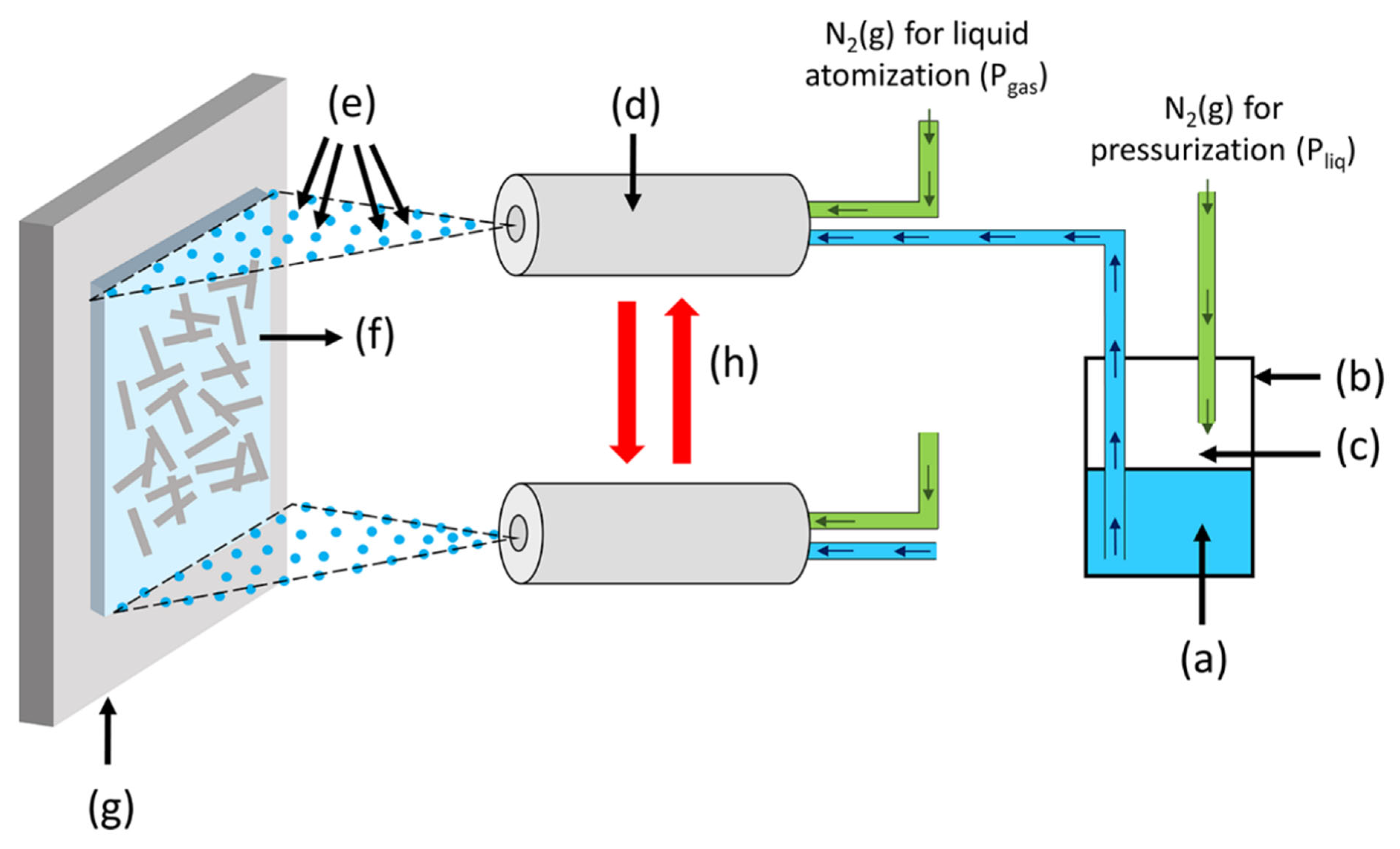
3.2.2. Spraying Method

The spraying technique is compatible with a wide range of substrate materials and enables efficient, large-area film production. Furthermore, films with varying thicknesses can be fabricated by adjusting the spraying duration, the concentration of the dispersion liquid, and the number of spraying cycles according to specific requirements. Spraying results in randomly oriented AgNWs, forming networks that facilitate relatively uniform current distribution. This configuration enables uniform voltage/current distribution and good electrical homogeneity. However, this method requires controlling the distance between the nozzle and the substrate and also faces challenges such as overspray material loss and nozzle clogging [30,31,32,33]. This preparation method involves the direct deposition of the AgNW dispersion liquid onto the entire substrate to form a film, as depicted in Figure 2.
Crêpellière et al. [31] deposited AgNWs on a preheated glass substrate using spray coating. After spraying for 3 min, uniform coverage was achieved over an area of 100 cm2, forming a dense conductive network. The performance parameters of the obtained AgNW networks were as follows: a sheet resistance of 9 Ω/sq, a visible light transmittance of 91.7%, and a haze factor of 3.7%. At the same performance level, their coverage area (100 cm2) exceeded that of most small-area preparation methods reported in the literature.
Gholami et al. [32] prepared a composite film of polystyrene (PS) embedded with AgNWs using a spray deposition method and further coated the AgNWs with a gold layer via double-pulse electrodeposition, resulting in a PS-AgNW@Au composite electrode. The test results indicated that the composite electrode exhibited a sheet resistance of 24 Ω/sq and a visible light transmittance of 84%. In repeated bending tests with a 4 mm radius, the resistance increased by only 22% after 2000 bends. The composite structure demonstrated excellent chemical stability, high conductivity, good optical transmittance, and outstanding flexibility.
Zheng et al. [33] developed a straightforward spray-assisted method to achieve an ordered arrangement of AgNWs. Compared to conventional AgNW electrodes, the ordered arrangement of electrodes showed significant improvements. The conventional electrode achieved a visible light transmittance of 86.6% and a sheet resistance of 18.3 Ω/sq, whereas the ordered arrangement electrode exhibited a visible light transmittance of 85% and a sheet resistance of 63 Ω/sq. Electrochemical impedance spectroscopy (EIS) confirmed that the optimization of electrode conductivity was the key factor. The orderly arrangement formed an efficient conductive network by reducing the percolation threshold, providing a low-resistance, high-permeability electrode solution for electrochromic devices.

3.2.3. Spin-Coating Method

The spin-coating process involves key steps to ensure a uniform film. Initially, the AgNW dispersion is applied to the substrate, which is then secured on a high-speed rotating turntable. The centrifugal force generated by the spinning action spreads the liquid evenly, resulting in a consistent film. However, spin-coating technology is characterized by high material loss and limited control over film thickness. Achieving film uniformity requires precise control of parameters such as solution concentration, spin-coating speed, and duration [30,31,32,33,34,35,36].
Song et al. [34] fabricated innovative WOx/AgNW FTCFs on a flexible polyethylene naphthalate (PEN) substrate using a solution method and spin-coating process. The key feature of the film is the incorporation of an ultrathin WOx layer, which effectively inhibits the oxidation of AgNWs by physically encapsulating the AgNW networks while significantly enhancing the mechanical flexibility and adhesion of the film to the PEN substrate. Due to the multifunctional protection and reinforcement provided by the WOx layer, the composite film exhibits exceptional properties: a sheet resistance as low as 9.4 Ω/sq, a visible light transmittance of 82.6%, outstanding mechanical stability (resistance change of less than 10% after 1000 bending cycles at a radius of 5 mm or adhesive tape peeling tests), and environmental stability (stable under high temperature, high humidity, and strong oxidative conditions).
Shi [35] fabricated a flexible transparent conductive film on a polyethylene terephthalate (PET) substrate using a two-step spin-coating method. After six spin-coating layers, AgNWs with a diameter of 40 nm achieved a performance breakthrough: a sheet resistance of 13 Ω/sq and a transmittance of 89.7% at 550 nm (haze of 4.23%). The diameter of AgNWs plays a critical role in determining the performance of the conductive network. Under identical area coverage, smaller-diameter AgNWs (20 nm) form a denser conductive network, resulting in a significantly lower sheet resistance (24.8 Ω/sq) compared to larger-diameter AgNWs (60 nm, 62.4 Ω/sq). The film demonstrates excellent stability (sheet resistance change rate of less than 10% after 1000 bending cycles) and superior infrared performance.
Wang et al. [36] developed an innovative MXene/AgNW/graphene sandwich-structured hybrid TCF via spin coating. MXene served as an intermediate layer to enhance adhesion, while graphene acted as a top protective layer, filling the AgNW network to improve conductivity, surface flatness, and stability. The composite film exhibited a transmittance of 87.5% at 550 nm and a sheet resistance of 14.4 Ω/sq. Additional advantages include low surface roughness, strong adhesion, and high stability.

3.2.4. Silk-Screen Printing

Silk-screen printing provides an efficient and cost-effective method for depositing films on various substrates. The process consists of several key steps: First, a screen with a customized pattern is prepared, while AgNWs are dispersed into a suitable ink formulation. This ink is then deposited onto the screen, where pressure from a squeegee enables the ink to pass through the screen’s mesh and transfer onto the substrate, thereby forming a AgNW film. This versatile printing technique is particularly suitable for producing intricate patterns, making it valuable for manufacturing flexible printed circuit boards and flexible thin-film transistors [37].
Li et al. [38] fabricated a large-area (15 × 20 cm2) AgNW transparent conductive film with high uniformity using silk-screen printing (HPMC/AgNW ink/98t mesh template). By optimizing the AgNW concentration to refine the conductive network, the film demonstrated superior performance, including low sheet resistance (13.0 ± 0.6 Ω/sq), high transmittance (95.3% at 550 nm), low haze (3.86%), and high flatness (surface roughness: 3.33 nm). The film was successfully employed in constructing a low-voltage-driven transparent heater, exhibiting excellent heating uniformity and long-term stability.
Xu et al. [39] developed a preparation method for AgNW/graphene oxide (GO) hybrid transparent electrodes based on silk-screen printing. The functional design of the electrode structure was achieved by alternately printing AgNW and GO layers. The resulting electrode exhibited high conductivity (11.9 Ω/sq), high visible light transmittance (83.5% at 550 nm), and outstanding mechanical flexibility. Its key advantages stem from the triple protection mechanism provided by the GO layer: (1) an antioxidant barrier (preventing environmental degradation and maintaining stable performance after thermal oxidation treatment), (2) a mechanical buffer layer (resistance change rate < 5% after 1500 bending cycles), and (3) biological interface isolation (avoiding direct contact between AgNWs and skin to enhance biocompatibility).
Li et al. [40] successfully fabricated films with low sheet resistance (1.1~9.2 Ω/sq) and high transmittance (75.2%~92.6%) by precisely controlling the screen mesh count (325 mesh) and AgNW ink thickness (10 μm). This process innovatively combines a low-concentration ink formulation with flash rapid sintering technology to simultaneously achieve high resolution, excellent conductivity, and optical properties in large-area (20 × 20 cm2) printing, making it well-suited for large-scale manufacturing applications.

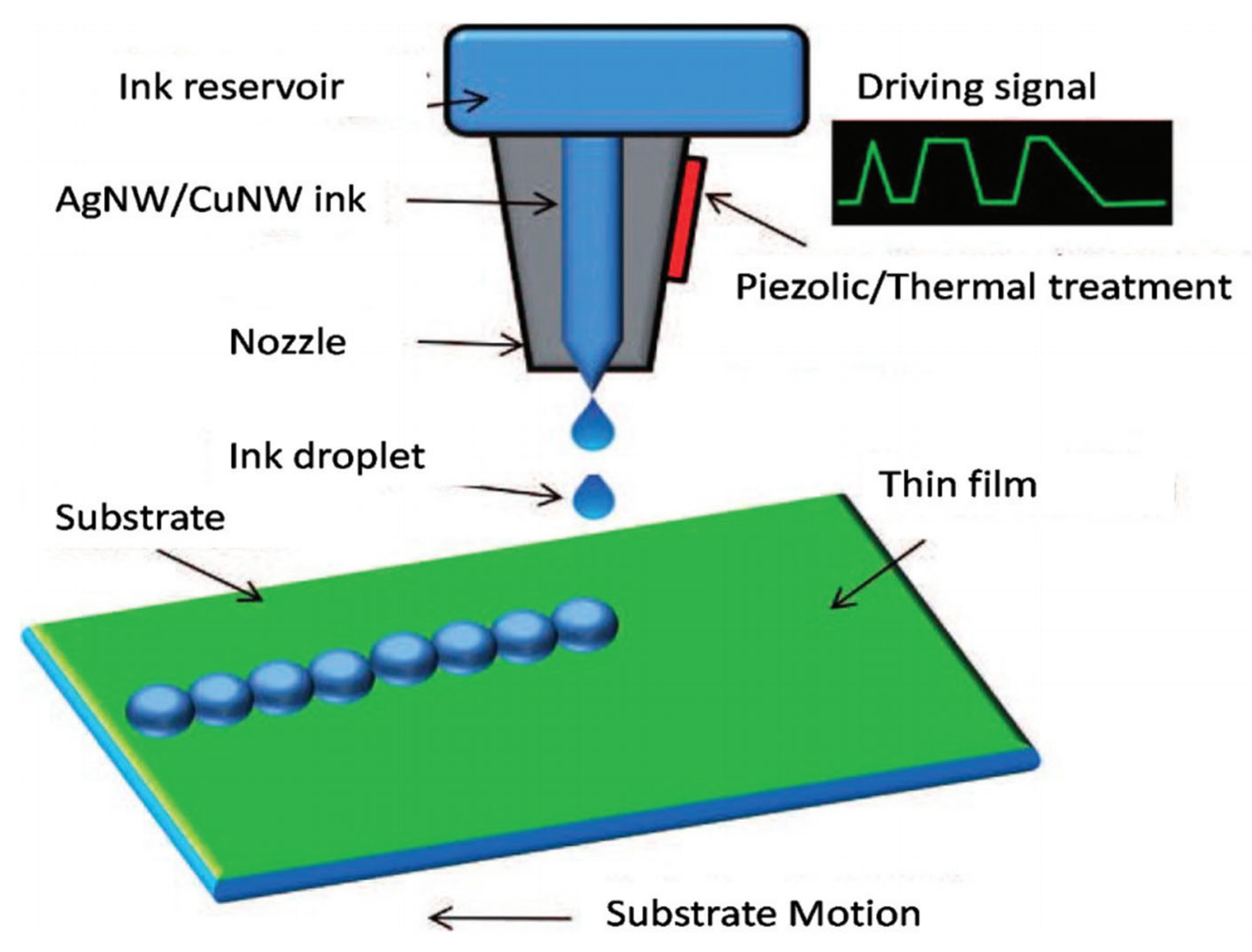
3.2.5. Inkjet Printing Method

Inkjet printing represents an innovative technology with significant market potential in the domain of large-area flexible and stretchable electronics. This process involves converting conductive film materials into conductive inks, which are then rapidly deposited onto a substrate through specialized nozzles to form a TCF. As illustrated in Figure 3, this method offers several advantages: it enables the creation of complex patterns without etching processes, facilitates rapid film formation, and is user-friendly. Additionally, it achieves a high material utilization rate.
Wang et al. [42] developed AgNW inks suitable for inkjet printing and successfully fabricated high-performance AgNW-TCFs on PET substrates. The films exhibited both low sheet resistance (13 Ω/sq) and high transmittance (81.9%) at 550 nm. Their excellent patterning capability and conductive reliability were demonstrated through the precise printing of heart-shaped patterns.
Wu et al. [43] employed inkjet printing technology and innovatively utilized AgNWs with an aspect ratio of 1000, incorporating modified polysilane lubricant to prepare functional ink. By precisely controlling the equipment temperature and ink concentration (thereby inhibiting AgNW aggregation), they successfully fabricated AgNW-TCFs with tunable optoelectronic properties. The transmittance ranged from 83.1% to 88.4% at a wavelength of 550 nm, while the sheet resistance was precisely adjusted within the range of 34.0~78.3 Ω/sq. Additionally, the films demonstrated outstanding mechanical stability, with a resistance change rate of less than 2.5% after 1000 bending cycles.
To further investigate the influence of deposition density on the performance of AgNW films, the figure of merit (FOM) was introduced to evaluate the comprehensive performance (transparent conductivity) of the TCF. The commonly adopted model is the ratio of direct current (DC) conductivity (σdc) to optical conductivity (σop), expressed as σdc/σop, which was considered in this study [44,45]. This ratio can also be calculated from the sheet resistance and optical transmittance using Equation (1).
F O M = σ d c σ op = Z 0 / [ 2 R s ( T a v 1 / 2 1 ) ]
Z0 represents the impedance of free space, which is a physical constant with a value of 376.7 Ω. Rs denotes the sheet resistance, measured in Ω/sq. Tav represents visible light (400~800 nm) transmittance. A higher FOM value corresponds to better optoelectronic performance of the FTCFs, reflecting both high electrical conductivity and excellent optical transmittance.
Based on the data obtained from the aforementioned preparation methods of AgNWs and following Equation (1), the calculation results of the FOM for AgNW films prepared by various methods are presented in Table 1.
Table 1 presents the performance parameters of various thin-film deposition methods, including Tav, Rs, FOM, and corresponding references. Mayer rod coating achieves high Tav values (92.2% and 91%) and relatively low Rs values (12.9 Ω/sq and 10 Ω/sq). This combination results in higher FOM values (352.33 and 390.08), indicating favorable performance in terms of transparent conductivity. Spraying demonstrates Tav values around 84% and Rs values of 24 Ω/sq or 12.95 Ω/sq, yielding lower FOM values (86.16 and 165.55), which may be attributed to film uniformity issues. Spin coating exhibits Tav values ranging from 82.6% to 87.5% and Rs values between 9.4 Ω/sq and 14.4 Ω/sq, producing FOM values of 199.78 and 189.44, representing a balance between conductivity and transmittance. Silk-screen printing demonstrates superior performance with a Tav of 95.3%, Rs of 13.6 Ω/sq, and the highest FOM (568.47), suggesting excellent comprehensive performance. Inkjet printing shows significant variability, with Tav values of 83.1% and 81.9% and Rs values of 34.0 Ω/sq and 13 Ω/sq, resulting in FOM values of 57.12 and 138, highlighting its sensitivity to process parameters. Overall, each method exhibits distinct advantages and limitations, guiding selection based on application requirements for transparency, conductivity, and process control.
From Table 2, in the realm of AgNW film preparation, the process characteristics of different methodologies diverge significantly owing to disparities in their underlying mechanisms. Spin coating and inkjet printing theoretically enable exceptionally high film uniformity through dynamic solution spreading or precise ink droplet positioning. Nevertheless, the former is constrained by uneven centrifugal force distribution at the edges of large-area substrates, while the latter is susceptible to nozzle clogging and ink rheological properties, necessitating rigorous regulation of operational parameters to achieve practical uniformity. The uniformity of spraying and silk-screen printing hinges directly on equipment precision, with spray stability and screen squeegee pressure uniformity serving as critical control factors, respectively.
In terms of thickness control, spin coating (via adjustments in rotation speed and solution concentration) and inkjet printing (via the design of ink droplet volume and deposition layers) can both achieve submicron-level precision, rendering them suitable for fabricating ultrathin or multilayer composite structures. Conversely, silk-screen printing and spraying technologies are better suited for preparing medium-to-thick films due to their process characteristics. The former relies on screen mesh count and paste viscosity, while the latter adjusts film thickness through spray volume and number of passes, meeting the requirements for large-area uniform coatings.
Notable differences also emerge in equipment cost and production efficiency: Mayer rod coating and silk-screen printing entail lower basic equipment costs, with the latter enabling high-speed large-area patterning production when integrated with automated production lines, making it ideal for low-cost industrial mass production. Inkjet printing (particularly industrial-grade high-precision systems) and spraying (automated spraying lines) incur medium-to-high costs. The former is more appropriate for small-area high-precision patterning due to printing speed limitations, while the latter serves as an efficient choice for large-area substrates (e.g., solar cells, architectural glass) under its continuous coating capability.
In summary, spin coating is the method of choice in laboratory research scenarios due to its advantage in producing high-quality films in small areas. In industrial applications, the selection diverges based on requirements: silk-screen printing is suitable for large-area patterning production, spraying technology caters to large-area low-cost coating preparation, and inkjet printing demonstrates unique advantages in constructing high-precision complex structures (e.g., flexible electronics, biosensors) through its precise positioning capability. This exemplifies the process adaptation logic from fundamental research to engineering applications.

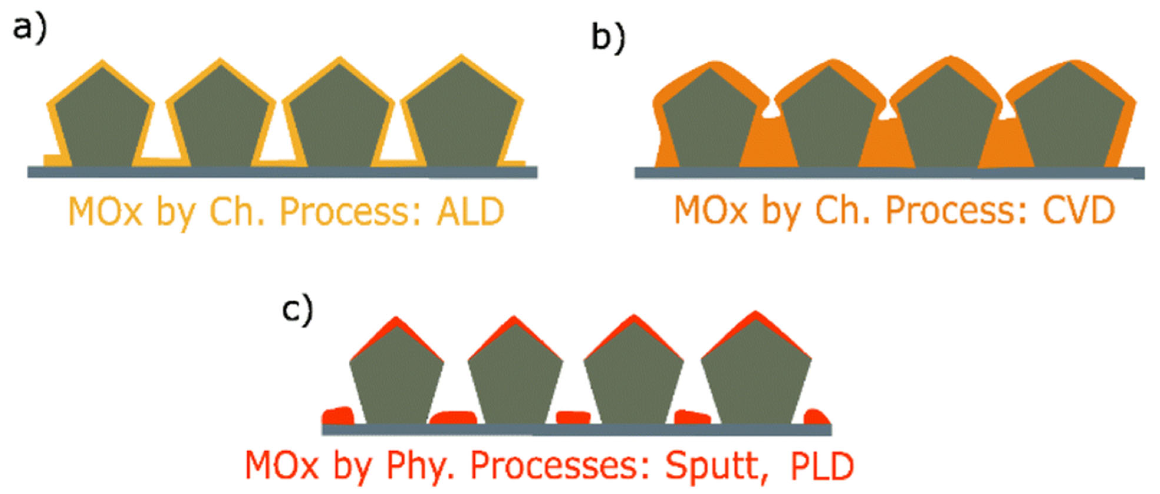
4. Methods for Coating AgNW Networks with Metal Oxides

AgNW networks, as emerging structures for constructing efficient TCEs, demonstrate significant potential for future technological development. However, these networks exhibit limitations such as inadequate thermal, chemical, and electrical stability. For example, AgNWs are susceptible to oxidation and agglomeration, exhibit relatively high interfacial contact resistance, and require optimization in terms of surface roughness. Metal oxide (MOx) coatings represent a promising enhancement strategy for AgNW networks. This approach improves oxidation resistance and thermal stability, modifies optical and electrical properties, and reduces interfacial contact resistance, thereby improving overall network performance.
The methods for enhancing the performance of AgNW networks through MOx coatings can be broadly categorized into two groups, physical processes and chemical processes, as illustrated in Figure 4. The following section provides a detailed explanation, incorporating the characteristics, advantages, and application scenarios of each process.

4.1. Physical Vapor Deposition Methods

Physical vapor deposition (PVD) methods are widely used for coating AgNW networks with MOx. These methods involve the transfer of material in the vapor phase and subsequent deposition onto the AgNW surface, as shown in Figure 4c.

4.1.1. Sputtering Deposition

As an efficient PVD technology, sputtering deposition utilizes high-energy ions to bombard metal oxide targets in a plasma environment, depositing sputtered particles onto the surface of AgNW networks. This method offers three principal advantages: high deposition rate, nanoscale thickness control, and excellent coating uniformity. However, this technology requires a high-vacuum environment and may potentially damage the microstructure of AgNWs through high-energy particle bombardment.
Qiu et al. [47] fabricated a high-aspect-ratio AgNW network (aspect ratio > 2000) by depositing silver onto an electrospun PVA nanofiber network via magnetron sputtering. By further employing polyvinylidene fluoride (PVDF) encapsulation, they simultaneously enhanced visible light transmittance (95.24%), conductivity (3.2 Ω/sq), and environmental stability. This approach effectively resolved the trade-off between optical transmission and electromagnetic shielding performance inherent in conventional materials.
Wu et al. [48] utilized radio-frequency magnetron sputtering to deposit aluminum-doped ZnO (AZO) onto spin-coated AgNW films. Through optimization of AgNW content (0.8 wt%), substrate temperature, and sputtering pressure, the AZO/AgNW stacked films achieved a resistivity of 2.15 × 10⁻⁴ Ω·cm and 80.28% transmittance in the 400~800 nm wavelength range. These films were subsequently fabricated into 2.4 GHz wideband transparent antennas for Bluetooth communication. This demonstrates sputtering’s capability to enhance film crystallinity and compactness through elevated substrate temperatures and reduced pressures, thereby improving both electrical conductivity and optical transmittance.

4.1.2. Pulsed Layer Deposition (PLD)

Generally, AgNWs are first prepared, dispersed, and deposited on a substrate before being placed in a PLD chamber. Laser pulses are used to bombard metal or metal oxide targets (such as ZnO and TiO2), causing the generated plasma to deposit films on the surface of AgNWs. This method can enhance the stability of AgNWs, improve interfacial properties, and regulate optical properties, which are utilized to prepare high-performance composite electrodes. However, it faces challenges such as difficulty in achieving uniform film coating and insufficient interfacial bonding strength.
Zhao et al. [49] overcame the single-function limitation of traditional metal sensors by developing a multifunctional silver nanoporous sensing platform based on pulsed laser deposition technology. The microstructure can be precisely controlled by adjusting the deposition parameters, enabling the simultaneous achievement of high-sensitivity strain sensing (interface optimization to broaden the detection range), surface-enhanced Raman scattering (SERS) for trace detection (nanoporous substrate-enhanced Raman signal), and significant antibacterial activity (silver ion slow release with an antibacterial rate > 99%). This platform integrates mechanical sensing, molecular recognition, and biosafety functions, offering a multi-scenario collaborative monitoring solution for wearable electronic devices.
PVD plays a critical role in coating MOx on AgNW networks. Sputtering deposition, which involves bombarding MOx targets with energetic ions in a plasma environment, enables rapid and precise control over the deposition of uniform coatings. This method currently holds significant application potential in fields such as transparent electromagnetic shielding (e.g., wearable devices) and flexible optoelectronics (e.g., transparent antennas). PLD deposits films on AgNWs via laser-pulse bombardment, enhancing stability and performance, though it faces challenges in coating uniformity and interfacial bonding. Overall, despite operational challenges, PVD methods enable precise control of coating properties, significantly improving the performance of AgNW networks in optoelectronics and sensing applications.

4.2. Chemical Deposition Methods

Chemical deposition methods rely on chemical reactions to deposit MOx on the AgNW networks. These methods often operate under relatively mild conditions and can be more suitable for large-scale production, as illustrated in Figure 4a,b.

4.2.1. Chemical Vapor Deposition (CVD)

CVD, with metal–organic chemical vapor deposition (MOCVD) as a variant using organometallic precursors, typically involves three sequential steps: vaporization of organometallic compounds to generate gaseous precursors, transportation of these vapors by a carrier gas to the substrate, and thermal decomposition of precursors on the substrate to form a continuous inorganic film through nucleation and growth. This process of controlled precursor reaction to achieve homogeneous coating is schematically shown in Figure 5 [50].

4.2.2. Atomic Layer Deposition (ALD)

ALD, a subclass of CVD, is a vapor-phase deposition technique based on surface-confined chemical reactions with self-limiting characteristics. It enables atomic-level, precise growth (0.1~1 nm per cycle) of MOx (e.g., Al2O3, TiO2, ZnO) on AgNW surfaces through the periodic alternating introduction of metal precursors (e.g., trimethylaluminum, TMA; titanium isopropoxide, TIPT) and reactive gases (e.g., H2O, O2).
Li et al. [51] successfully fabricated nonpolar ZnO optical films using ALD combined with a thermal annealing process. Their study demonstrated that the AgNW/ZnO composite electrode prepared after 500 deposition cycles exhibited superior thermal stability: after heating at 400 °C for 180 min, the electrode maintained a high transmittance exceeding 95% in the visible spectrum (380~780 nm), while the sheet resistance increased only to 1.9 times its initial value. This performance was significantly better than that of pure AgNW electrodes without ZnO protection.
Weng et al. [52] employed ALD to deposit a 30 nm thick, three-dimensional conformal TiO2 coating on AgNWs and PDMS substrates, forming a AgNWs@TiO2 composite film. This composite film exhibited outstanding properties: a visible light transmittance of 75% (380~780 nm) and a transmittance retention exceeding 95% after 500 bending cycles (5 mm curvature radius). The results indicated that the TiO2 coating not only enhanced the interfacial adhesion between AgNWs and the PDMS substrate but also significantly improved the thermal stability and oxidation resistance of the composite film due to its barrier effect.

4.2.3. Solution Methods

Solution methods primarily include electrochemical deposition and sol–gel synthesis. In electrochemical deposition, Ag+ ions in an electrolyte are reduced on the cathode surface under an external electric field, enabling directional growth of AgNWs. In the sol–gel process, reducing agents (e.g., sodium borohydride) reduce silver ions in salt solutions to nanoscale particles, which are stabilized by additives such as PVP to form AgNWs. Stabilizers, including PVP, are employed to regulate particle aggregation, forming a sol that gradually undergoes gelation and finally solidifies into AgNWs. Both processes exhibit low deposition rates, typically in the range of approximately 0.1 to 10 nm/min.
Kang et al. [53] successfully fabricated high-performance AgNW/ZnO composite electrodes by spraying AgNWs and spin coating a 0.45 M low-temperature sol–gel ZnO precursor, followed by annealing at 150 °C for 0.5 h. While maintaining excellent photoelectric performance (average visible light transmittance of 84%, sheet resistance of 30~50 Ω/sq), the surface RMS roughness of the electrode was significantly reduced from 21.2 nm to 8.5 nm. Notably, the ZnO-modified layer endowed the electrode with exceptional mechanical stability (sheet resistance remained at 44.3 Ω/sq after 10,000 bending cycles at a 7.5 mm curvature radius) and chemical stability (effectively inhibiting Ag migration), providing a reliable electrode solution for large-area printing of flexible solar cells.
Jang et al. [54] fabricated large-area (2 × 2 cm2) and uniformly cross-linked AgNW films on a Au substrate using a micro-upgraded AgNW suspension via a solution-based method. When employed as a substrate for SERS, the hot-spot density could be effectively modulated by adjusting experimental parameters. The SERS enhancement effect of these films was significantly superior to that of drop-cast AgNW films with the same surface density, exhibiting an enhancement factor of 1.8~36 times. Among the samples, the C-14 film (surface density of 8.3 μg/cm2) demonstrated optimal performance, along with excellent uniformity and reproducibility, suggesting potential applications in optoelectronics, nanoelectronics, and sensor technologies.
Chemical deposition methods, which involve depositing MOx onto AgNW networks via chemical reactions, are characterized by mild reaction conditions and excellent scalability for large-scale manufacturing. These techniques enable a wide range of strategies to customize the optoelectronic properties, surface topography, and durability of AgNW-based composites. Consequently, they demonstrate significant potential for applications in flexible electronics, optoelectronic devices, and other emerging technological fields.

4.3. Hybrid Approaches

Hybrid techniques combine physical deposition and chemical synthesis to deposit thin films on substrates. Initially, a liquid solution coats the surface to ensure uniform dispersion and complete coverage. Subsequently, a curing step initiates chemical processes that remove residual solvents and promote the formation of the final coating. This process enables efficient fabrication and performance optimization of AgNW-based films.
From Table 3, different AgNW film preparation methods exhibit distinct characteristics in film uniformity, equipment cost, production efficiency, and applicable scenarios. Sputtering deposition provides excellent, dense, regularly structured films with high equipment cost and medium production efficiency, making it suitable for TCEs in displays and solar cells. PLD ensures excellent, precise patterning but involves very high equipment cost and low small-area production efficiency, rendering it ideal for high-performance electronic devices such as gas sensors and high-frequency components. CVD can produce high-quality thin films over large areas. Although the equipment cost is very high, the large-scale production efficiency is also high, making it more suitable for flexible electronic devices, including flexible displays and wearable devices. ALD offers extremely high atomic-level film uniformity, though with very high equipment cost and low layer-by-layer deposition efficiency, making it applicable to high-stability electrodes such as lithium-battery electrodes and UV photodetectors. Solution methods, featuring low equipment cost and relatively high production efficiency, typically yield films with a porous structure. These films are applicable in flexible wearable devices (e.g., flexible circuits, biosensors) and low-cost optoelectronic devices.
Oxide coatings can modify AgNW networks through ALD, sol–gel, and other technologies, significantly impacting their performance. On the positive side, oxide coatings can substantially enhance the thermal stability of silver nanowires (e.g., ZnO coatings can limit the resistance increase after heating at 400 °C to 1.9 times [51]), as well as chemical stability (e.g., TiO2 coatings can mitigate the effects of sulfidation corrosion [47]) and mechanical stability (reducing the risk of bending and fracture). Additionally, they optimize optoelectronic performance (regulating visible light transmittance and enhancing surface plasmon effects [53]) and improve interface compatibility (reducing roughness and inhibiting Ag+ ion migration [53]).
However, negative effects may arise, including increased resistance (thick coatings hinder electron conduction [52]), minor degradation of optical properties (reduced UV absorption or visible light transmittance [51,52]), and greater process complexity and cost [47,50]. These drawbacks can be mitigated through optimization strategies, such as controlling coating thickness (e.g., 30 nm TiO2 or ZnO for 500 ALD cycles [51,52]), selecting scenario-appropriate oxides (ZnO for UV response, TiO2 for chemical stability requirements [51,52]), or designing composite coatings.
Overall, oxide coatings represent an effective approach to improving the comprehensive performance of silver nanowire networks, particularly in applications with stringent stability requirements, thereby expanding their utility in flexible electronics, sensors, and related fields.

5. Application of AgNW-TCFs

ITO has long been the mainstream transparent conductor due to its excellent photoelectric performance. However, its inherent brittleness, high cost, and the scarcity of indium resources limit its application in flexible devices [55]. In contrast, AgNWs exhibit superior conductivity (often exceeding that of ITO) and good optical transmittance [56,57,58], while possessing natural mechanical flexibility that enables adaptation to bending, torsion, and other deformations [59]. Although AgNWs require polymer modification to optimize contact resistance and enhance stability against environmental oxidation and corrosion [60,61], ITO—while chemically stable—is prone to fracture in flexible applications. Consequently, ITO remains more suitable for traditional rigid devices, whereas AgNWs have emerged as the preferred choice for flexible optoelectronic devices due to their inherent flexibility and the potential application of polymer protective layers.
Due to trends such as the lightweight, thin, flexible, and high-performance nature of electronic devices, advancements in touch screen technology, and improvements in the efficiency of solar cells, AgNWs have significant application potential across various fields. This is attributed to their exceptional properties, including high optical transmittance, electrical conductivity, flexibility, and stability. In recent years, the maturation of their preparation processes has resulted in reduced costs and an expanded market scale. Furthermore, AgNWs align with the principles of environmental protection and sustainable development, offering promising prospects for commercial applications. For example, they can play a crucial role in areas such as organic light-emitting diodes, solar cells, flexible sensors, and electromagnetic shielding.

5.1. Displays/Touch Screens

AgNW film is widely used in the field of displays and touch screens. Its core advantages include excellent electrical conductivity, high-precision touch sensitivity, and support for advanced functions such as force sensing [62]; exceptional flexibility that meets the requirements of flexible displays, making it particularly suitable for foldable devices and curved screens [63]; and an open conductive grid structure that ensures outstanding optical clarity [63].
Cho et al. [59] proposed an improved rod coating technique enabling large-area (>20 × 20 cm2) fabrication of cross-aligned AgNW networks. These networks exhibited a sheet resistance of 21.0 Ω/sq and a visible light transmittance of 95.0%, outperforming random networks, as shown in Figure 6. By integrating this network with a mechanochromic spiropyran-polydimethylsiloxane composite film, they developed a flexible, transparent touch screen with force-sensitive response capabilities. This touch screen can accurately monitor dynamic writing, track patterns, and perceive local variations in writing force, providing a novel platform for multifunctional flexible optoelectronic devices.
Yu et al. [64] developed a flexible transparent electrode based on AgNWs and sulfhydryl-modified nanocellulose (nfc-hs). The electrode significantly improved substrate adhesion through Ag-S bonding, while demonstrating excellent visible light transmittance (81.34% at 600 nm), conductivity (sheet resistance of 30 Ω/sq), and stability. The electrode maintained its performance after 10,000 bending cycles and 60 peel tests. When implemented in flexible touch screen panels (f-TSPs), the electrode withstood over 500 bending cycles (3 mm bending radius) without significant degradation, substantially enhancing device durability. This study presents a novel strategy for developing next-generation, high-durability flexible electronic devices.
Zhang et al. [65] spin-coated a polyol-synthesized AgNW solution onto glass substrates for 30 s, followed by coating with a 10 wt% PVDF N, N-dimethylformamide (DMF) solution on annealed AgNW films. The resulting PVDF/AgNW electrodes exhibited superior conductivity (sheet resistance of 4.6~17.2 Ω/sq), visible light transmittance (85% at 550 nm), and long-term stability. After 1000 bending cycles (0°~180°), the sheet resistance increased by only 28%. Wearable microcircuits, electronic skins, and biomechanical energy harvesters fabricated using these PVDF/AgNW electrodes demonstrated exceptional performance characteristics.

5.2. Lighting and Organic Light-Emitting Diodes (OLEDs)

As a novel TCE, AgNW networks have demonstrated significant advantages in flexible OLED applications. Compared with conventional ITO, AgNW electrodes can be fabricated over large areas through low-temperature solution processes (e.g., spin coating and spray coating), making them compatible with flexible substrates such as polyimide (PI) and PET, thereby overcoming the inherent brittleness limitation of ITO.
Du et al. [66] fabricated a AgNW film exhibiting a low sheet resistance of 26.5 Ω/sq, a high visible light transmittance of 95.2% (at 550 nm), and a root-mean-square roughness of 5.4 nm via xenon lamp beam irradiation. Additionally, they produced a large-area flexible OLED (25 × 25 mm2) demonstrating an external quantum efficiency (EQE) of 22.2% and a luminous efficacy of 78.0 cd/A.
Wang et al. [67] developed a Ti3C2Tₓ/AgNW/PEDOT-PET composite film electrode through a spraying method, achieving a low sheet resistance (<30 Ω/sq) and high visible light transmittance (>80%) at 550 nm wavelength. This electrode utilized a sandwich conductive structure composed of a AgNW network, a novel two-dimensional nanosheet (possessing excellent electrical conductivity, hydrophilicity, and mechanical flexibility), and PEDOT:PSS. The resulting flexible OLED with this composite anode exhibited a maximum brightness of 10,040 cd/m2, a maximum current efficiency of 3.7 cd/A, and a current density of 535.5 mA/cm2. Low-temperature welding (80 °C) of AgNWs was achieved using Ti3C2Tₓ surface functional groups, preventing thermal damage to the substrate. The sandwich structure design optimized conductive network connectivity, surface roughness, and environmental stability, offering a high-performance ITO alternative for flexible wearable devices and foldable displays.
Qian et al. [68] constructed TCFs with HPMC/AgNW/GP sandwich structures based on HPMC. The film demonstrated a high transmittance of 81.5% and a low sheet resistance of 4.2 Ω/sq at 550 nm, surpassing the performance of comparable AgNW-TCFs. As an OLED anode, the device exhibited superior luminous performance and stability, achieving a maximum brightness of 13,740 cd/m2, a maximum current efficiency of 10.6 cd/A, a maximum power efficiency of 5.5 lm/W, and a maximum EQE of 2.9%. The GP layer enhanced charge transfer by improving hydrophilicity, while the HPMC encapsulation layer simultaneously reduced surface roughness and enhanced flexibility, presenting a novel strategy for high-performance flexible optoelectronic devices.
Table 4 enumerates a range of materials, highlighting variations in performance parameters such as turn-on voltage, maximum current efficiency, and maximum luminous brightness. These variations underscore the diverse optoelectronic properties inherent to different materials.

5.3. Organic Solar Cells (OSCs)

Flexible TCEs are essential components of foldable organic solar cells (FOSCs), as their performance directly affects the optoelectronic conversion efficiency of these devices. AgNWs demonstrate superior electrical conductivity and optical transparency on flexible substrates, and their fabrication process is relatively simple. When utilized in the production of TCEs for solar cells, AgNWs not only improve the conversion efficiency but also substantially lower manufacturing costs. The basic structure of FOSCs is shown in Figure 7.
Lei et al. [75] developed FOSCs based on AgNW composite transparent electrodes. By doping 6 vol% EG into PEDOT:PSS PH1000 to optimize electrode performance, the device achieved a photoelectric conversion efficiency (PCE) of 10.30%. In mechanical stability tests, the device retained 90% of its initial PCE after 1000 bending cycles, with a PCE retention rate exceeding 75% after 180° complete folding.
Song et al. [76] introduced ultra-flexible and ultra-light OSCs with a total thickness of less than 3 μm and a weight of 4.83 g/m2. By incorporating a ternary strategy using PC71BM as the third component, they reduced crystallization and agglomeration in the active layer, improving ductility and achieving a stable PCE of 15.5% and a weight power ratio of 32.07 W/g. After 800 compression cycles, the device retained over 83% of its PCE, and after 1000 h of storage in a nitrogen environment, the PCE remained above 95%, establishing a foundation for integrating flexible power supplies with wearable electronics.
Qi et al. [77] prepared cross-aligned AgNWs via a one-step method and embedded them in biodegradable elastic polyester (PGSU) to construct a hybrid electrode (visible light transmittance at 550 nm ≈ 90%, sheet resistance 52.6 Ω/sq). By controlling the solvent evaporation rate of the perovskite precursor solution, the electrode minimized nucleation and formed a dense, large-grain perovskite film, improving the PCE of flexible and degradable PSCs to 17.51%, comparable to traditional top-electrode-based devices (16.86%). The device exhibited excellent mechanical flexibility (93.2% PCE retention after 500 bending cycles at a 9.3 mm radius) and environmental sustainability (complete degradation within one week), offering a new strategy for eco-friendly flexible optoelectronic devices.

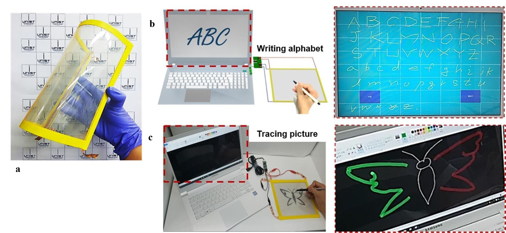
5.4. Flexible Sensors

The sensor can continuously monitor the operational status of electronic equipment. Among these, the flexible sensor can assess human health, with performance indicators including responsiveness, sensitivity, hysteresis, and stability. Among metal nanowires, AgNWs exhibit superior electrical and thermal conductivity, along with notable resistance to oxidation and corrosion. Consequently, AgNW-TCFs are utilized in the fabrication of devices such as conductive patches and biosensors, providing more convenient and efficient solutions for medical diagnostics and treatment.
Qin et al. [78] prepared a AgNW/MXene/non-woven fabric composite material using the dip-coating technique for application in a pressure sensor. The unique sandwich structure exhibits high sensitivity (14.28 kPa−1 within the pressure range of 0.25 to 5 kPa), a wide sensing range (0.25 to 400 kPa), rapid response and recovery times (60 ms/120 ms), excellent stability, and long-term durability for human motion detection applications.
Chen et al. [79] employed a liquid film rupture-assisted self-assembly method to fabricate conductive leaf veins from AgNWs, achieving a low sheet resistance of 3.6 Ω/sq and high transparency of 79%. The pressure sensor based on these conductive leaf veins demonstrates a sensitivity of 3.8 kPa−1 and enables real-time monitoring of human motion, showing significant potential for applications such as motion tracking and information encryption.
Castillo-López et al. [80] deposited AgNWs in PVA via drop-coating. The resulting sensor operates within an applied force range of 0 to 3.92 N, with a sensitivity of 0.039 N−1, and effectively detects force variations even under minimal external stimulation.

5.5. Electromagnetic Shielding

Due to their high electrical conductivity, flexibility, and transparency, AgNWs have emerged as leading candidates for next-generation electromagnetic shielding materials, with the potential to advance the development of future electronic devices toward lighter, thinner, and more intelligent designs.
Jiang et al. [81] successfully fabricated a flexible, high-performance electromagnetic interference (EMI) shielding film that can be rapidly produced and is adaptable to various environments. By employing a scraping and coating technique with aramid nanofibers (ANF) and spraying AgNWs to form a sandwich structure, the shielding effectiveness reached 50.6 dB with the addition of 1.0 mg/cm2 of AgNWs. The film demonstrated excellent performance in both acidic and alkaline environments, offering a new direction for the development of ultrathin, high-performance EMI shielding films with promising application potential.
Guo et al. [82] successfully synthesized a composite film with an efficient EMI SE of 84.3 dB and a low reflection coefficient of 0.42 using a highly controllable vacuum-assisted filtration technique. The composite film consisted of a low-electrical-conductivity CoFe2O4@MXene hybrid aggregated in the top region as an impedance matching layer and highly conductive AgNWs deposited at the bottom as an efficient shielding layer. Furthermore, the ratio of absorption loss (SEA) to total shielding effectiveness (SET) was significantly higher than the ratio of reflection loss (SER) to SET.
Nguyen et al. [83] demonstrated a successful approach to developing multifunctional EMI shielding materials through the structural design of multilayer composite films. The film was prepared by sequentially performing vacuum filtration on suspensions of graphene fluoride (GF)@ANF and AgNWs@ANF. The EMI SE of the film within the X-band frequency range reached 54 dB while achieving an ultrahigh in-plane thermal conductivity exceeding 45 W/mK.

5.6. Other Important Applications

Materials based on AgNWs also demonstrate significant potential in other critical applications, including low-emissivity films, transparent heaters, and computational memory. For instance, low-emissivity films fabricated by tailoring the network density and distribution of AgNWs achieve efficient reflection of long-wave infrared radiation (8~14 μm band) while maintaining high visible light transmittance, making them essential for energy-efficient architectural glazing, automotive windshields, and thermal management systems in electronic devices [84]. Meanwhile, transparent heaters based on AgNW composites leverage their high electrical conductivity and flexibility, integrated into flexible substrates such as PET or PDMS, to enable uniform heat distribution and rapid heating response. These find promising applications in defogging/defrosting devices, flexible displays, and wearable thermal therapy systems (e.g., flexible electronic skins for promoting transdermal drug absorption via localized heating) [85]. Additionally, AgNW-based resistive random-access memory (RRAM) devices utilize the formation and rupture mechanisms of nanoscale conductive filaments to achieve high integration density and low power consumption, with the potential for neuromorphic computing by modulating the electrochemical reactions at the AgNW–oxide interface to simulate synaptic behaviors. Collectively, these applications highlight the interdisciplinary versatility of AgNWs, driven by their unique electrical, optical, and structural properties [86].

6. Stability Challenges and Mitigation in AgNW Networks

6.1. The Degradation Mechanism of AgNWs

The stability of AgNW networks under various stress conditions remains a critical challenge for their practical implementation. Recent studies have highlighted four primary instability mechanisms: electrical instability, thermal failure, photodegradation, and chemical corrosion.

6.1.1. Electrical Instability

Electrical instability in AgNW networks primarily arises from electromigration and Joule heating effects. Under continuous current flow, AgNW networks experience electromigration effects, leading to localized heating and eventual breakdown of nanowire junctions. Under DC stress, electron wind drives Ag+ ions to migrate, forming Ag2O/AgOH precipitates at the anode and dendritic growths at the cathode, resulting in localized breakages [87,88]. Grazioli et al. [89] simulated that AgNW networks fail instantaneously at 0.5 A due to Joule heating-induced melting, whereas AC operation mitigates this effect by reducing directional ion movement.

6.1.2. Thermal Failure

Elevated temperatures accelerate oxidation processes and promote nanowire coalescence through surface diffusion. This results in increased junction resistance and network fragmentation over time. Thermal degradation of AgNWs is governed by the Rayleigh instability.
Ag electrodes were stable up to 200 °C, showing no degradation in optical properties or loss of conductivity. However, as the annealing temperature was further increased, the optical and electrical properties of the bare Ag nanowire electrode degraded significantly. After annealing at 380 °C, the transmittance decreased from 90.7% to 85.0%, and the haze increased from 1.24% to 7.29% [90].
Jeong et al. [91] reported that unencapsulated AgNW-TCFs exhibited a significant increase in sheet resistance from 75~80 Ω/sq to over 700 Ω/sq after 4 days of thermal aging at 150 °C, which was attributed to the diffusion-mediated surface aggregation (DMSA) effect. Notably, the degradation process was accelerated under elevated temperatures and light exposure, ultimately leading to a complete loss of conductivity.

6.1.3. Photodegradation

Under long-term light exposure, AgNW networks exhibit unique and complex behaviors that distinguish them from other electrode materials. UV irradiation can induce surface plasmon resonance, generating a photo-thermal effect in AgNWs. This photo-thermal effect elevates local temperatures within AgNW networks, creating “hot spots” that accelerate sulfidation and oxidation. Additionally, synergistic UV/O3 exposure produces oxides such as AgO2, disrupting the nanowire nanostructure and consequently degrading both transmittance and conductivity.
Lin et al. [92] investigated the degradation of AgNW-TCFs (initial sheet resistance ~30 Ω/sq) under ultraviolet A (UVA) exposure. The resistance increased to 200 Ω/sq after 16 h (75 °C), 24 h (60 °C), and 60 h (45 °C) of UVA exposure, compared to 288 h under high damp heat (85 °C/85% humidity) without UVA, confirming that UVA accelerates TCF performance degradation.

6.1.4. Chemical Corrosion

The degradation mechanism of AgNWs in air is analogous to that of bulk silver: chemical corrosion is primarily driven by interactions between their surface and atmospheric components. Exposure to atmospheric sulfur compounds and moisture induces silver sulfide formation, significantly impairing conductivity. Yan et al. [93] recently reported that AgNWs in perovskite solar cells undergo corrosion by specific perovskite precursor components (e.g., methylammonium iodide) and the MAPbI3 layer itself, with the extent of corrosion varying under different environmental conditions.
AgNW networks suffer from four interrelated degradation mechanisms under operational and environmental stresses:
(1)
Electrical instability: Driven by electromigration and Joule heating under DC bias, this mechanism induces Ag+ ion migration, dendritic growth, and junction failure. AC operation partially mitigates directional ion transport.
(2)
Thermal failure: At elevated temperatures (>200 °C), Rayleigh instability and surface diffusion are activated, leading to nanowire coalescence, increased junction resistance, and optical haze.
(3)
Photodegradation: UV-induced plasmonic heating accelerates oxidation/sulfidation, forming conductive hot spots and structural defects.
(4)
Chemical corrosion: Exposure to atmospheric sulfur, moisture, or reactive layers (e.g., MAPbI3) converts AgNWs into insulating Ag2S, degrading conductivity.
These mechanisms often coexist synergistically, exacerbating real-world stability challenges. While stability is critical for optoelectronic device performance, achieving it requires addressing multifactorial degradation pathways, as isolated solutions fail under concurrent thermal, electrical, and environmental stressors.

6.2. Mitigation Strategies

To enhance the stability of AgNW-TCFs, four advanced strategies have been developed.

6.2.1. Surface Encapsulation

ALD: TCFs based on AgNWs with fine encapsulation layers prepared using materials exhibiting excellent thermal stability, such as Al2O3, TiO2, ZnO, GO, and reduced graphene oxide (rGO), can effectively inhibit the diffusion of silver atoms at elevated temperatures, thereby enhancing the thermal stability of AgNW networks.
Yeh et al. [94] directly deposited a layer of TiO2 on AgNWs coated with PVP via ALD. PVP serves as a nucleation foundation for TiO2 during the ALD process. The AgNW-TCFs with a conformal TiO2 protective layer exhibit stability for up to 100 h under heat treatment at 200 °C. When the temperature increases to 300 °C, their thermal stability improves by more than two orders of magnitude compared to unprotected films.

6.2.2. Stabilization Additives

Entifar et al. [95] demonstrated that TEs treated with 11-aminoundecanoic acid exhibit a low sheet resistance of 26 Ω/sq, high transmittance of 90%, and exceptional stretchability, with resistance variation maintained within approximately 10% under 120% stretching. Additionally, the introduction of a conductive PEDOT:PSS overlayer significantly enhances the chemical stability of the stretchable AgNW films.

6.2.3. Hybrid Nanocomposites

CNT Reinforcement: Interpenetrating CNT networks maintain electrical percolation under thermal stress.
Pillai et al. [96] demonstrated that the single-walled carbon nanotube (SWCNT)–AgNW–resin–PET film electrode exhibits a peak current of approximately 470 μA at 0.8 V, which is an order of magnitude higher than that of the AgNW electrode (~46 μA). The hybrid film retains a sheet resistance of ~30 Ω/sq without mechanical degradation after 1000 bending cycles at an 8 mm radius, exhibiting nearly identical performance to unbend samples.

6.2.4. Process Optimization

Tang et al. [97] demonstrated that AgNW/ZnO composite TCEs processed via low-temperature solution exhibit excellent flexibility, environmental and thermal stability (approximately 300 °C), high electrical conductivity (~20 Ω/sq), and good transmittance (~87% at 550 nm). This low-temperature process successfully balances the key properties of high conductivity, high transmittance, low roughness, and high stability, and its comprehensive performance is significantly better than that of pure AgNW electrodes and commercial ITO material.
Choo et al. [98] coated GO sheets onto AgNW electrodes using a simple dipping method to prevent UV irradiation and ozone from contacting the AgNW surface, thereby suppressing the increase in sheet resistance in GO-treated AgNWs. GO and other coating materials are used to isolate environmental factors and inhibit UV-induced degradation. At the same time, the heat treatment process is optimized to avoid the temperature exceeding 160 °C to maintain network integrity. The visible light transmittance decreased from 94% to 88%, but the transverse surface plasmon resonance (TSPR) peak was retained.
These strategies collectively address multifactorial degradation mechanisms, balancing optoelectronic performance with environmental and mechanical resilience, thereby advancing AgNW networks toward practical applications in flexible electronics and energy devices.

6.3. Future Challenges and Research Directions

Future research on metal nanowire (MNW) networks should prioritize three areas [99]:
  • Dynamic Failure Modeling: Develop multiscale models (nano to macro) simulating real-time failure processes, such as hot-spot diffusion under electrothermal stress. Integrate microscale mechanisms (e.g., Rayleigh instability, electromigration) with macroscale transport behavior to enable predictive analysis of failure propagation.
  • Standardized Testing: Establish unified lifetime metrics (e.g., time-to-failure, TTF) under multi-stress conditions (thermal/chemical/mechanical coupling), replacing single extreme tests. Standardize reporting of degradation kinetics (e.g., cyclic resistance changes).
  • Process Optimization: Deploy roll-to-roll (R2R) compatible encapsulation technologies (e.g., atomic layer deposition, ALD; GO) to enhance coating uniformity, reduce ALD energy use, and lower GO processing costs for scalable manufacturing. This will ensure cost-effective reliability across flexible electronics and optoelectronic applications.

7. Conclusions and Outlook

7.1. Conclusions

This article reviews the research progress of AgNW-TCFs. Recent studies demonstrate that AgNW thin films exhibit visible light transmittance exceeding 90% and sheet resistance as low as 15 Ω/sq and maintain stable optoelectronic properties after more than 10,000 bending cycles, making them highly valuable for applications. Current fabrication methods—including Mayer rod coating, spraying, spin coating, silk-screen printing, and inkjet printing—offer low-cost, scalable production of large-area AgNW films (200 × 200 mm2). Furthermore, surface encapsulation (e.g., ALD-deposited ZnO/TiO2), hybrid composites (MXene/AgNW/graphene), and network densification techniques significantly enhance the oxidation resistance of AgNW films. Consequently, AgNW films show promising potential for applications in touch screens, OLEDs, OSCs, flexible sensors, and EMI shielding.

7.2. Outlook and Future Directions

Despite notable advancements, AgNW-TCFs still face critical challenges in large-area uniformity, long-term stability, and cost-effectiveness, which require targeted solutions. One major issue is achieving nanometer-level uniformity over large areas. This necessitates improvements in processes compatible with R2R operations, such as silk-screen printing and spraying. Additionally, better control over film thickness is essential. The long-term stability of the material is also a concern, especially when exposed to high temperatures exceeding 200 °C, UV radiation, and chemical stress. Reliable packaging strategies are crucial, including the use of a GO/AgNW composite or depositing an Al2O3/TiO2 barrier via ALD. Furthermore, enhancing cost-effectiveness is vital for commercialization. This can be achieved by optimizing network density, reducing silver consumption, utilizing low-cost ink formulations (such as HPMC/AgNW), developing inexpensive precursors, and employing energy-efficient synthesis methods like microwave-assisted microfluidic techniques.
AgNW-TCFs demonstrate significant potential for application and are advancing in several emerging fields:
(1)
Biomedical Electronics: AgNW electrodes with antibacterial properties have been developed and utilized in wearable biosensors and smart bandages.
(2)
Energy Systems: AgNW integrated electrodes significantly enhance the charge transfer dynamics in fuel cells and supercapacitors.
(3)
Intelligent Environments: A large area of AgNW-TCFs enables energy-saving smart windows to achieve dynamic and adjustable emissivity control.
(4)
Neuromorphic Computing: AgNW-based RRAM offers a solution for low-power neuromorphic synaptic devices.
In the future, the synergy of material innovation, process engineering, and interdisciplinary applications will drive the development of AgNW-TCFs toward high-performance and sustainable flexible electronics, ultimately meeting the diverse needs of consumer electronics, health care, and green energy.

Author Contributions

J.L. (Ji Li): methodology, software, writing—original draft. J.L. (Jun Luo): conceptualization, data curation, funding acquisition. Y.L.: writing—review and editing, supervision. All authors have read and agreed to the published version of the manuscript.

Funding

This work is supported by the Natural Science Planning Project of Xiaogan (Grant No. XGKJ2023010062), Joint Project of Xiaogan Social Science Association and Research Center of Hubei Micro and Small Enterprise Development (grant number LH202417), and the Natural Science Foundation of Hubei Province (Grant No. 2023AFB944).

Institutional Review Board Statement

Not applicable.

Informed Consent Statement

Not applicable.

Data Availability Statement

The original contributions presented in this study are included in the article. Further inquiries can be directed to the corresponding author.

Conflicts of Interest

The authors declare no conflicts of interest.

References

  1. Kim, K.S.; Kim, S.O.; Han, C.J.; Kim, D.U.; Kim, J.S.; Yu, Y.T.; Lee, C.R.; Kim, J.W. Revisiting the thickness reduction approach for near-foldable capacitive touch sensors based on a single layer of Ag nanowire-polymer composite structure. Compos. Sci. Technol. 2018, 165, 58–65. [Google Scholar] [CrossRef]
  2. Maji, A.; Kuila, C.; Panda, B.; Dhak, D.; Murmu, N.C.; Kuila, T. Tailoring AgNWs-rGO/PVDF advanced composites for flexible strain sensors in wearable electronics with thermal management: Balancing sensitivity and hysteresis. ACS Appl. Electron. Mater. 2025, 7, 1670–1683. [Google Scholar] [CrossRef]
  3. Wu, Z.; Niu, Z.; Wang, Y.; Xu, Z.; Liu, Y.; Wang, W.; Li, S. Flexible OLED Performance Enhancement: The impact of AgNWs: AgNPs electrode-integrated MoOX QDs hole-injection layer. ACS Appl. Mater. Interfaces 2025, 17, 10898–10906. [Google Scholar] [CrossRef] [PubMed]
  4. Wan, J.; Chen, Y.; Chen, W.; Xia, J.; Zeng, G.; Cao, J.; Jin, C.; Shen, Y.; Wu, X.; Chen, H.; et al. Enhanced charge collection of AgNWs-based top electrode to realize high-performance, all-solution processed organic solar cells. Sci. China Chem. 2024, 67, 3347–3356. [Google Scholar] [CrossRef]
  5. Zhang, X.; Dai, H.; Ji, M.; Han, Y.; Jiang, B.; Cheng, C.; Song, X.; Song, Y.; Wu, G. A flexible piezoresistive strain sensor based on AgNWs/MXene/PDMS sponge. J. Mater. Sci. Mater. Electron. 2025, 36, 452. [Google Scholar] [CrossRef]
  6. Wu, B.; Yu, Y.; Wu, P.; Wu, Y.; Huang, J.; Song, X. SiC whisker/AgNWs/TPU composite film with asymmetric structure for low-reflection electromagnetic interference shielding. J. Appl. Polym. Sci. 2024, 141, e56019. [Google Scholar] [CrossRef]
  7. Sharma, V.; Arora, E.K.; Jaison, M.; Vashist, T.; Jagtap, S.; Adhikari, A.; Kumar, P.; Dash, J.K.; Patel, R. Tuning the work function and properties of the conducting polymer PEDOT:PSS for enhancing optoelectronic device performance of solar cells and organic light emitting diodes. Polym. Plast. Technol. Mater. 2025, 64, 1019–1045. [Google Scholar] [CrossRef]
  8. Azadmehr, S.; Alamdari, S.; Tafreshi, M.J. Flexible and transparent highly luminescent sensor based on doped zinc tungstate/graphene oxide nanocomposite. Eur. Phys. J. Plus 2025, 140, 284. [Google Scholar] [CrossRef]
  9. Achagri, G.; Ismail, R.; Kadier, A.; Ma, P.C. A solar-powered electrocoagulation process with a novel CNT/silver nanowire coated basalt fabric cathode for effective oil/water separation: From fundamentals to application. J. Environ. Manag. 2025, 375, 124289. [Google Scholar] [CrossRef] [PubMed]
  10. He, W.; Ye, C. Flexible Transparent Conductive Films on the Basis of Ag Nanowires: Design and Applications: A Review. J. Mater. Sci. Technol. 2015, 31, 581–588. [Google Scholar] [CrossRef]
  11. Hou, S.; Liu, J.; Shi, F.; Zhao, G.X.; Tan, J.W.; Wang, G. Recent Advances in Silver Nanowires Electrodes for Flexible Organic/Perovskite Light-Emitting Diodes. Front. Chem. 2022, 10, 864186. [Google Scholar] [CrossRef] [PubMed]
  12. Guo, Z.; Li, X.; Li, N.; Liu, X.; Li, H.; Li, X.; Wang, Y.; Liang, J.; Chen, Z. Multilayer directionally arranged silver nanowire networks for flexible transparent conductive films. Phys. Chem. Chem. Phys. 2023, 25, 14778. [Google Scholar] [CrossRef] [PubMed]
  13. Tao, J.; Liu, N.; Li, S.; Shi, J.; Ji, S. Structural manipulation of silver nanowire transparent conductive films for optoelectrical property optimization in different application fields. Thin Solid Film. 2021, 729, 138679. [Google Scholar] [CrossRef]
  14. Chen, X.; Zhang, Y.; Ma, C.; Liu, H. Large-area, stretchable, ordered silver nanowires electrode by superwetting-induced transfer of ionic liquid@silver nanowires complex. Chem. Eng. J. 2023, 476, 146505. [Google Scholar] [CrossRef]
  15. Zhang, P.; Tong, X.; Gao, Y.; Qian, Z.; Ren, R.; Bian, C.; Wang, J.; Cai, G. A sensing and stretchable polymer-dispersed liquid crystal device based on spiderweb-inspired silver nanowires-micromesh transparent electrode. Adv. Funct. Mater. 2023, 33, 2303270. [Google Scholar] [CrossRef]
  16. Tang, Q.; Zou, M.; Chang, L.; Guo, W. A super-flexible and transparent wood film/silver nanowire electrode for optical and capacitive dual-mode sensing wood-based electronic skin. Chem. Eng. J. 2022, 430, 132152. [Google Scholar] [CrossRef]
  17. Hao, T.; Zhang, L.; Ji, H.; Zhou, Q.; Feng, T.; Song, S.; Wang, B.; Liu, D.; Ren, Z.; Liu, W.; et al. A stretchable, transparent, and mechanically robust silver nanowire-polydimethylsiloxane electrode for electrochromic devices. Polymers 2023, 15, 2640. [Google Scholar] [CrossRef] [PubMed]
  18. Wang, X.; Song, C.; Wang, Y.; Feng, S.; Xu, D.; Hao, T.; Xu, H. Flexible transparent films of oriented silver nanowires for a stretchable strain sensor. Materials 2024, 17, 4059. [Google Scholar] [CrossRef] [PubMed]
  19. Kim, D.H.; Yu, K.C.; Kim, Y.; Kim, J.W. Highly stretchable and mechanically stable transparent electrode based on composite of silver nanowires and polyurethane-urea. ACS Appl. Mater. Interfaces 2015, 7, 15214–15222. [Google Scholar] [CrossRef] [PubMed]
  20. Thomas, N.; Sharma, N.; Swaminathan, P. Optimizing silver nanowire dimensions by the modification of polyol synthesis for the fabrication of transparent conducting films. Nanotechnology 2023, 35, 055602. [Google Scholar] [CrossRef] [PubMed]
  21. Ge, Y.; Liu, J.; Liu, X.; Hu, J.; Duan, X.; Duan, X. Rapid electrochemical cleaning silver nanowire thin films for high-performance transparent conductors. J. Am. Chem. Soc. 2019, 141, 12251–12257. [Google Scholar] [CrossRef] [PubMed]
  22. Zhang, C.; Li, C.; Si, X.; He, Z.; Qi, J.; Feng, J.; Cao, J. Single-crystalline silver nanowire arrays directly synthesized onto substrates by template-assisted chemical wetting. Materialia 2020, 9, 100529. [Google Scholar] [CrossRef]
  23. Song, M.; Zhou, X.; He, X.; Cao, H.; Liu, J.; Qiu, H.; Jin, Z. Distance dependent fluorescence enhancement of silver nanowires deposited on AAO. Opt. Mater. 2018, 83, 241–244. [Google Scholar] [CrossRef]
  24. Bleiji, Y.; Cordaro, A.; Tabernig, S.W.; Alarcón-Lladó, E. High Aspect Ratio Silver Nanogrids by Bottom-Up Electrochemical Growth as Transparent Electrode. ACS Appl. Opt. Mater. 2024, 2, 508–516. [Google Scholar] [CrossRef] [PubMed]
  25. Sekhar, S.C.; Nagaraju, G.; Yu, J.S. Conductive silver nanowires-fenced carbon cloth fibers-supported layered double hydroxide nanosheets as a flexible and binder-free electrode for high-performance asymmetric supercapacitors. Nano Energy 2017, 36, 3658–3667. [Google Scholar] [CrossRef]
  26. Wang, L.; Kong, Y.; Zhang, Z.; Luo, G.; Hou, X.; Su, A.; Yang, X.; Wu, K.J. Streamlined Synthesis of Silver Nanowires Using Multi-Objective Optimization for Electrically Conductive Composite Filaments. Adv. Funct. Mater. 2024, 34, 2407999. [Google Scholar] [CrossRef]
  27. Kaabipour, S.; Hemmati, S. Continuous, green, and room-temperature synthesis of silver nanowires in a helically-coiled millifluidic reactor. Colloids Surf. A Physicochem. Eng. Asp. 2023, 659, 130806. [Google Scholar] [CrossRef]
  28. Zhou, L.; Yu, M.; Yao, L.; Lai, W.Y. Mayer rod-coated organic light-emitting devices: Binary solvent inks, film topography optimization, and large-area fabrication. Adv. Eng. Mater. 2022, 24, 2101558. [Google Scholar] [CrossRef]
  29. Zhang, S.; Liu, X.; Lin, T.; He, P. A method to fabricate uniform silver nanowires transparent electrode using meyer rod coating and dynamic heating. J. Mater. Sci. Mater. Electron. 2019, 30, 18702–18709. [Google Scholar] [CrossRef]
  30. Sannicolo, T.; Charvin, N.; Flandin, L.; Kraus, S.; Papanastasiou, D.T.; Celle, C.; Simonato, J.P.; Munoz-Rojas, D.; Jiménez, C.; Bellet, D. Electrical mapping of silver nanowire networks: A versatile tool for imaging network homogeneity and degradation dynamics during failure. ACS Nano 2018, 12, 4648–4659. [Google Scholar] [CrossRef] [PubMed]
  31. Crepelliere, J.; Menguelti, K.; Wack, S.; Bouton, O.; Gerard, M.; Popa, P.L.; Pistillo, B.R.; Leturcq, R.; Michel, M. Spray deposition of silver nanowires on large area substrates for transparent electrodes. ACS Appl. Nano Mater. 2021, 4, 1126–1135. [Google Scholar] [CrossRef]
  32. Gholami, M.; Tajabadi, F.; Taghavinia, N.; Moshfegh, A. Chemically-stable flexible transparent electrode: Gold-electrodeposited on embedded silver nanowires. Sci. Rep. 2023, 13, 17511. [Google Scholar] [CrossRef] [PubMed]
  33. Zheng, J.; Zhao, Y.; Chen, L.; Zheng, Y.; Wang, X.; Xu, G.; Xiao, X. Unveiling the function and mechanism of the ordered alignment silver nanowires on boosting the electrochromic performance. Chem. Eng. J. 2023, 463, 142524. [Google Scholar] [CrossRef]
  34. Song, L.; Qu, S.; Ma, L.; Yu, S. All solution prepared WOx/AgNW composite transparent conductive films with enhanced adhesion and stability. Mater. Lett. 2023, 336, 133918. [Google Scholar] [CrossRef]
  35. Shi, L. Flexible transparent silver nanowires conductive films fabricated with spin-coating method. Micro Nano Lett. 2022, 18, e12151. [Google Scholar] [CrossRef]
  36. Wang, P.; Jian, M.; Wu, M.; Zhang, C.; Zhou, C.; Ling, X.; Zhang, J.; Yang, L. Highly sandwich-structured silver nanowire hybrid transparent conductive films for flexible transparent heater applications. Compos. Part A Appl. Sci. Manuf. 2022, 159, 106998. [Google Scholar] [CrossRef]
  37. Correia, V.; Mitra, K.Y.; Castro, H.; Rocha, J.G.; Sowade, E.; Baumann, R.R.; Lanceros-Méndez, S. Design and fabrication of multilayer inkjet-printed passive components for printed electronics circuit development. J. Manuf. Process. 2018, 31, 364–371. [Google Scholar] [CrossRef]
  38. Li, Z.; Zhang, X.; Shan, J.; Liu, C.; Guo, X.; Zhao, X.; Yang, H. Facile fabrication of large-scale silver nanowire transparent conductive films by screen printing. Mater. Res. Express 2022, 9, 066401. [Google Scholar] [CrossRef]
  39. Xu, X.; Liu, Z.; He, P.; Yang, J. Screen-printed silver nanowire and graphene oxide hybrid transparent electrodes for long-term electrocardiography monitoring. J. Phys. D Appl. Phys. 2019, 52, 455401. [Google Scholar] [CrossRef]
  40. Li, W.; Yarali, E.; Bakytbekov, A.; Anthopoulos, T.D.; Shamim, A. Highly transparent and conductive electrodes enabled by scalable printing. Nanotechnology 2020, 31, 395201. [Google Scholar] [CrossRef] [PubMed]
  41. Khan, S.; Ali, S.; Bermak, A. Smart manufacturing technologies for printed electronics. In Hybrid Nanomaterials; IntechOpen: Rijeka, Croatia, 2020; p. 148. [Google Scholar] [CrossRef]
  42. Wang, Y.; Wu, X.; Wang, K.; Lin, K.; Xie, H.; Zhang, X.; Li, J. Novel insights into inkjet printed silver nanowires flexible transparent Conductive Films. Int. J. Mol. Sci. 2021, 22, 7719. [Google Scholar] [CrossRef] [PubMed]
  43. Wu, X.; Wang, S.; Luo, Z.; Lu, J.; Lin, K.; Xie, H.; Wang, Y.; Li, J.Z. Inkjet printing of flexible transparent conductive films with silver nanowires ink. Nanomaterials 2021, 11, 1571. [Google Scholar] [CrossRef] [PubMed]
  44. Al-Milaji, K.N.; Huang, Q.; Li, Z.; Ng, T.N.; Zhao, H. Direct Embedment and alignment of silver nanowires by Inkjet printing for stretchable conductors. ACS Appl. Electron. Mater. 2020, 2, 3289–3298. [Google Scholar] [CrossRef]
  45. Jia, L.C.; Yan, D.X.; Liu, X.; Ma, R.; Wu, H.Y.; Li, Z.M. Highly efficient and reliable transparent electromagnetic interference shielding film. ACS Appl. Mater. Interfaces 2018, 10, 11941–11949. [Google Scholar] [CrossRef] [PubMed]
  46. Sekkat, A.; Sanchez-Velasquez, C.; Bardet, L.; Weber, M.; Jiménez, C.; Bellet, D.; Muñoz-Rojas, D.; Nguyen, V.H. Towards enhanced transparent conductive nanocomposites based on metallic nanowire networks coated with metal oxides: A brief review. J. Mater. Chem. A 2024, 12, 25600–25621. [Google Scholar] [CrossRef]
  47. Qiu, R.; Zheng, H.; Zhao, X.; Yang, P.; Yu, S. The high transmittance silver nanowire conductive films with excellent electromagnetic shielding efficiency prepared by electrospinning and magnetron sputtering. Opt. Mater. 2024, 157, 116219. [Google Scholar] [CrossRef]
  48. Wu, C.T.; Ho, Y.R.; Huang, D.Z.; Huang, J.J. AZO/silver nanowire stacked films deposited by RF magnetron sputtering for transparent antenna. Surf. Coat. Technol. 2019, 360, 95–102. [Google Scholar] [CrossRef]
  49. Zhao, X.; Deng, Z.; Long, Y.; Feng, B.; Jiang, X.; Liu, X.; Zhong, Y.; Zou, S.; Zhen, Z.; Lin, S.; et al. Multifunctional sensing platform with pulsed-laser-deposited silver nanoporous structures. Sens. Actuators A. Phys. 2019, 293, 136–144. [Google Scholar] [CrossRef]
  50. Vikulova, E.S.; Dorovskikh, S.I.; Basova, T.V.; Zheravin, A.A.; Morozova, N.B. Silver CVD and ALD Precursors: Synthesis, Properties, and Application in Deposition Processes. Molecules 2024, 29, 5705. [Google Scholar] [CrossRef] [PubMed]
  51. Li, Z.; Li, Z.; Shi, Z.; Zhu, P.; Wang, Z.; Zhang, J.; Li, Y.; He, P.; Zhang, S. ALD prepared silver nanowire/ZnO thin film for ultraviolet detectors. Mater. Today Commun. 2023, 37, 106974. [Google Scholar] [CrossRef]
  52. Weng, Y.; Chen, G.; Zhou, X.; Zhang, Y.; Yan, Q.; Guo, T. Stability enhancement and patterning of silver nanowire networks by conformal TiO2 coating for flexible transparent conductive electrodes. J. Mater. Sci. 2023, 58, 17816–17828. [Google Scholar] [CrossRef]
  53. Kang, J.; Han, K.; Sun, X.; Zhang, L.; Huang, R.; Ismail, I.; Wang, Z.; Ding, C.; Zha, W.; Li, F.; et al. Suppression of Ag migration by low-temperature sol-gel zinc oxide in the Ag nanowires transparent electrode-based flexible perovskite solar cells. Org. Electron. 2020, 82, 105714. [Google Scholar] [CrossRef]
  54. Jang, S.; Lee, J.; Nam, S.; Ko, H.; Chang, S.T. Large-Area, Highly Sensitive SERS Substrates with Silver Nanowire Thin Films Coated by Microliter-Scale Solution Process. Nanoscale Res. Lett. 2017, 12, 581. [Google Scholar] [CrossRef] [PubMed]
  55. Galle, L.; Ehrling, S.; Lochmann, S.; Kaskel, S.; Bischoff, L.; Grothe, J. Conductive ITO Interfaces for Optoelectronic Applications Based on Highly Ordered Inverse Opal Thin Films. ChemNanoMat 2020, 6, 560–566. [Google Scholar] [CrossRef]
  56. Kumar, A.; Shaikh, M.O.; Chuang, C.H. Silver Nanowire Synthesis and Strategies for Fabricating Transparent Conducting Electrodes. Nanomaterials 2021, 11, 693. [Google Scholar] [CrossRef] [PubMed]
  57. Wang, B.Y.; Lee, E.S.; Oh, Y.J.; Kang, H.W. A silver nanowire mesh overcoated protection layer with graphene oxide as a transparent electrode for flexible organic solar cells. RSC Adv. 2017, 7, 52914–52922. [Google Scholar] [CrossRef]
  58. Jang, J.; Choi, J.Y.; Jeon, J.; Lee, J.; Im, J.; Lee, J.; Jin, S.W.; Park, H.J.; Lee, S.H.; Kim, D.B.; et al. Flexible Transparent Electrode Characteristics of Graphene Oxide/Cysteamine/AgNP/AgNW Structure. Nanomaterials 2020, 10, 2352. [Google Scholar] [CrossRef] [PubMed]
  59. Cho, S.; Kang, S.; Pandya, A.; Shanker, R.; Khan, Z.; Lee, Y.; Park, J.; Craig, S.L.; Ko, H. Large-area cross-aligned silver nanowire electrodes for flexible, transparent, and force-sensitive mechanochromic touch screens. ACS Nano 2017, 11, 4346–4357. [Google Scholar] [CrossRef] [PubMed]
  60. Hwang, B.; Qaiser, N.; Lee, C.; Matteini, P.; Yoo, S.J.; Kim, H. Effect of Al2O3/Alucone nanolayered composite overcoating on reliability of Ag nanowire electrodes under bending fatigue. J. Alloys Compd. 2020, 846, 156420. [Google Scholar] [CrossRef]
  61. Wang, P.; Jian, M.; Zhang, C.; Wu, M.; Ling, X.; Zhang, J.; Wei, B.; Yang, L. Highly Stable Graphene-Based Flexible Hybrid Transparent Conductive Electrodes for Organic Solar Cells. Adv. Mater. Interfaces 2021, 9, 2101442. [Google Scholar] [CrossRef]
  62. Jia, Y.; Chen, C.; Jia, D.; Li, S.; Ji, S.; Ye, C. Silver Nanowire Transparent Conductive Films with High Uniformity Fabricated via a Dynamic Heating Method. ACS Appl. Mater. Interfaces 2016, 8, 9865–9871. [Google Scholar] [CrossRef] [PubMed]
  63. Yoo, J.H.; Kim, Y.; Han, M.K.; Choi, S.; Song, K.Y.; Chung, K.C.; Kim, J.M.; Kwak, J. Silver Nanowire–Conducting Polymer–ITO Hybrids for Flexible and Transparent Conductive Electrodes with Excellent Durability. ACS Appl. Mater. Interfaces 2015, 7, 15928–15934. [Google Scholar] [CrossRef] [PubMed]
  64. Yu, H.; Tian, Y.; Dirican, M.; Fang, D.; Yan, C.; Xie, J.; Jia, D.; Liu, Y.; Li, C.; Cui, M.; et al. Flexible, transparent and tough silver nanowire/nanocellulose electrodes for flexible touch screen panels. Carbohydr. Polym. 2021, 273, 118539. [Google Scholar] [CrossRef] [PubMed]
  65. Zhang, L.; Wang, Y.; Gui, J.; Wang, X.; Li, R.; Liu, W.; Sun, C.; Zhao, X.; Guo, S. Efficient Welding of Silver Nanowires embedded in a Poly (vinylidene fluoride) Film for Robust Wearable Electronics. Adv. Mater. Technol. 2019, 4, 1800438. [Google Scholar] [CrossRef]
  66. Du, M.; Yang, Z.; Miao, Y.; Wang, C.; Dong, P.; Wang, H.; Guo, K. Facile nanowelding process for silver nanowire electrodes toward high-performance large-area flexible organic light-emitting diodes. Adv. Funct. Mater. 2024, 34, 2404567. [Google Scholar] [CrossRef]
  67. Wang, Y.; Liu, Y.; Wang, T.; Liu, S.; Chen, Z.; Duan, S. Low-temperature nanowelding silver nanowire hybrid flexible transparent conductive film for green light OLED devices. Nanotechnology 2022, 33, 455201. [Google Scholar] [CrossRef] [PubMed]
  68. Qian, P.F.; Geng, W.H.; Bao, Z.L.; Jing, L.C.; Zhang, D.; Geng, H.Z. Eco-friendly transparent conductive films formed by silver nanowires embedded with conductive polymers in HPMC for flexible OLEDs. Surf. Interfaces 2025, 56, 105583. [Google Scholar] [CrossRef]
  69. Kim, D.W.; Han, J.W.; Lim, K.T.; Kim, Y.H. Highly enhanced light-outcoupling efficiency in ITO-free organic light emitting diodes using surface nanostructure embedded high-refractive index polymers. ACS Appl. Mater. Interfaces 2018, 10, 985–991. [Google Scholar] [CrossRef] [PubMed]
  70. Kim, S.; Kim, J.; Kim, D.; Kim, B.; Chae, H.; Yi, H.; Hwang, B. High-performance transparent quantum dot light-emitting diode with patchable transparent electrodes. ACS Appl. Mater. Interfaces 2019, 11, 26333–26338. [Google Scholar] [CrossRef] [PubMed]
  71. Li, H.; Liu, Y.; Su, A.; Wang, J.; Duan, Y. Promising hybrid graphene-silver nanowire composite electrode for flexible organic light-emitting diodes. Sci. Rep. 2019, 9, 17998. [Google Scholar] [CrossRef] [PubMed]
  72. Triambulo, R.E.; Kim, J.H.; Park, J.W. Highly flexible organic light-emitting diodes on patterned Ag nanowire network transparent electrodes. Org. Electron. 2019, 71, 220–226. [Google Scholar] [CrossRef]
  73. Lian, L.; Dong, D.; Feng, D.; He, G. Low roughness silver nanowire flexible transparent electrode by low temperature solution-processing for organic light emitting diodes. Org. Electron. 2017, 49, 9–18. [Google Scholar] [CrossRef]
  74. Wang, Y.; Chen, Q.; Zhang, G.; Xiao, C.; Wei, Y.; Li, W. Ultrathin flexible transparent composite electrode via semi-embedding silver nanowires in a colorless polyimide for high performance ultraflexible organic solar cells. ACS Appl. Mater. Interfaces 2022, 14, 5699–5708. [Google Scholar] [CrossRef] [PubMed]
  75. Lei, T.; Peng, R.; Song, W.; Hong, L.; Huang, J.; Fei, N.; Ge, Z. Bendable and foldable flexible organic solar cells based on Ag nanowire films with 10.30% efficiency. J. Mater. Chem. A 2019, 7, 3737–3744. [Google Scholar] [CrossRef]
  76. Song, W.; Yu, K.; Zhou, E.; Xie, L.; Hong, L.; Ge, J.; Zhang, J.; Zhang, X.; Peng, R.; Ge, Z. Crumple durable ultra flexible organic solar cells with an excellent ower-per-weight performance. Adv. Funct. Mater. 2021, 31, 2102694. [Google Scholar] [CrossRef]
  77. Qi, J.; Chen, S.; Lan, C.; Wang, A.C.; Cui, X.; You, Z.; Zhang, Q.; Li, Y.; Wang, Z.L.; Wang, H.; et al. Large-grained perovskite films enabled by one-step meniscus-assisted solution printing of cross-aligned conductive nanowires for biodegradable flexible solar cells. Adv. Energy Mater. 2020, 10, 2001185. [Google Scholar] [CrossRef]
  78. Qin, W.; Xue, Y.; Li, G.; Peng, H.; Gong, G.; Yan, R.; Zhao, X.; Pang, J. Highly-sensitive wearable pressure sensor based on AgNWs/MXene/non-woven fabric. Org. Electron. 2024, 125, 106958. [Google Scholar] [CrossRef]
  79. Chen, X.; Jin, J.; Liu, B.; Li, S.; Guo, T.; Sheng, Z.; Wu, H. Flexible and transparent leaf-vein electrodes fabricated by liquid film rupture self-assembly AgNWs for application of heaters and pressure sensors. Chem. Eng. J. 2024, 499, 156500. [Google Scholar] [CrossRef]
  80. Castillo-López, D.N.; Gómez-Pavón, L.D.C.; Gutíerrez-Nava, A.; Zaca-Morán, P.; Arriaga-Arriaga, C.A.; Muñoz-Pacheco, J.M.; Luis-Ramos, A. Flexible force sensor based on a PVA/AgNWs nanocomposite and cellulose acetate. Sensors 2024, 24, 2819. [Google Scholar] [CrossRef] [PubMed]
  81. Jiang, X.; Cai, G.; Song, J.; Zhang, Y.; Yu, B.; Zhai, S.; Chen, K.; Zhang, H.; Yu, Y.; Qi, D. Large-scale fabrication of tunable sandwich-structured silver nanowires and aramid nanofiber films for exceptional electromagnetic interference (EMI) shielding. Polymers 2023, 16, 61. [Google Scholar] [CrossRef] [PubMed]
  82. Guo, Z.; Zhao, Y.; Luo, P.; Chen, Z.; Song, P.; Jin, Y.; Pei, L.; Ren, F.; Ren, P. Durable and sustainable CoFe2O4@MXene-silver nanowires/cellulose nanofibers composite films with controllable electric–magnetic gradient towards high-efficiency electromagnetic interference shielding and Joule heating capacity. Chem. Eng. J. 2024, 485, 149691. [Google Scholar] [CrossRef]
  83. Nguyen, D.K.; Pham, T.N.; Pham, A.L.H.; Nguyen, V.C.; Tran, M.S.; Bui, V.Q.; Vu, M.C. Multilayered silver nanowires and graphene fluoride-based aramid nanofibers for excellent thermosconductive electromagnetic interference shielding materials with low-reflection. Colloids Surf. A Physicochem. Eng. Asp. 2024, 688, 133553. [Google Scholar] [CrossRef]
  84. Hanauer, S.; Celle, C.; Crivello, C.; Szambolics, H.; Muñoz-Rojas, D.; Bellet, D.; Simonato, J.P. Transparent and Mechanically Resistant Silver-Nanowire-Based Low-Emissivity Coatings. ACS Appl. Mater. Interfaces 2021, 13, 21971–21978. [Google Scholar] [CrossRef] [PubMed]
  85. Choi, S.B.; Meena, J.S.; Joo, J.; Kim, J.W. Autonomous self-healing wearable flexible heaters enabled by innovative MXene/polycaprolactone composite fibrous networks and silver nanowires. Adv. Compos. Hybrid Mater. 2023, 6, 227. [Google Scholar] [CrossRef]
  86. Milano, G.; Pedretti, G.; Montano, K.; Ricci, S.; Hashemkhani, S.; Boarino, L.; Ielmini, D.; Ricciardi, C. In materia reservoir computing with a fully memristive architecture based on self-organizing nanowire networks. Nat. Mater. 2021, 21, 195–202. [Google Scholar] [CrossRef] [PubMed]
  87. Charvin, N.; Resende, J.; Papanastasiou, D.T.; Munoz-Rojas, D.; Jiménez, C.; Nourdine, A.; Bellet, D.; Flandin, L. Dynamic degradation of metallic nanowire networks under electrical stress: A comparison between experiments and simulations. Nanoscale Adv. 2021, 3, 675–681. [Google Scholar] [CrossRef] [PubMed]
  88. Grazioli, D.; Gangi, G.; Nicola, L.; Simone, A. Predicting mechanical and electrical failure of nanowire networks in flexible transparent electrodes. Compos. Sci. Technol. 2024, 245, 110304. [Google Scholar] [CrossRef]
  89. Oh, H.; Lee, J.; Lee, M. Transformation of silver nanowires into nanoparticles by rayleigh instability: Comparison between laser irradiation and heat treatment. Appl. Surf. Sci. 2018, 427, 65–73. [Google Scholar] [CrossRef]
  90. Hwang, B.; An, Y.; Lee, H.; Lee, E.; Becker, S.; Kim, Y.H.; Kim, H. Highly flexible and transparent Ag nanowire electrode encapsulated with Ultra-Thin Al2O3: Thermal, ambient, and mechanical stabilities. Sci. Rep. 2017, 7, 41336. [Google Scholar] [CrossRef] [PubMed]
  91. Jeong, Y.C.; Nam, J.; Kim, J.; Kim, C.S.; Jo, S. Enhancing thermal oxidation stability of silver nanowire transparent electrodes by using a cesium carbonate-incorporated overcoating layer. Materials 2019, 12, 1140. [Google Scholar] [CrossRef] [PubMed]
  92. Lin, C.C.; Lin, D.X.; Lin, S.H. Degradation problem in silver nanowire transparent electrodes caused by ultraviolet exposure. Nanotechnology 2020, 31, 215705. [Google Scholar] [CrossRef] [PubMed]
  93. Yan, Z.; Chen, H.; Li, M.; Wen, X.; Yang, Y.; Choy, W.C.; Lu, H. Observing and understanding the corrosion of silver nanowire electrode by precursor reagents and MAPbI3 film in different environmental conditions. Adv. Mater. Interfaces 2021, 8, 2001669. [Google Scholar] [CrossRef]
  94. Yeh, M.H.; Chen, P.H.; Yang, Y.C.; Chen, G.H.; Chen, H.S. Investigation of Ag-TiO2 interfacial reaction of highly stable Ag nanowire transparent conductive film with conformal TiO2 coating by atomic layer deposition. ACS Appl. Mater. Interfaces 2017, 9, 10788–10797. [Google Scholar] [CrossRef] [PubMed]
  95. Entifar, S.A.N.; Han, J.W.; Lee, D.J.; Ramadhan, Z.R.; Hong, J.; Kang, M.H.; Kim, S.; Lim, D.; Yun, C.; Kim, Y.H. Simultaneously enhanced optical, electrical, and mechanical properties of highly stretchable transparent silver nanowire electrodes using organic surface modifier. Sci. Technol. Adv. Mater. 2019, 20, 116–123. [Google Scholar] [CrossRef] [PubMed]
  96. Pillai, S.K.R.; Wang, J.; Wang, Y.; Sk, M.M.; Prakoso, A.B.; Rusli Chan-Park, M.B. Totally embedded hybrid thin films of carbon nanotubes and silver nanowires as flat homogenous flexible transparent conductors. Sci. Rep. 2016, 6, 38453. [Google Scholar] [CrossRef] [PubMed]
  97. Tang, Y.; Ruan, H.; Liu, H.; Zhang, J.; Shi, D.; Han, T.; Yang, L. Low-temperature solution processed flexible silver nanowires/ZnO composite electrode with enhanced performance and stability. J. Alloys Compd. 2018, 747, 659–665. [Google Scholar] [CrossRef]
  98. Choo, D.C.; Kim, T.W. Degradation mechanisms of silver nanowire electrodes under ultraviolet irradiation and heat treatment. Sci. Rep. 2017, 7, 1696. [Google Scholar] [CrossRef] [PubMed]
  99. Patil, J.J.; Chae, W.H.; Trebach, A.; Carter, K.J.; Lee, E.; Sannicolo, T.; Grossman, J.C. Failing Forward: Stability of Transparent Electrodes Based on Metal Nanowire Networks. Adv. Mater. 2020, 33, e2004356. [Google Scholar] [CrossRef] [PubMed]
Figure 1. Schematic illustration of AgNW-TCFs using the Mayer rod coating method [28].
Coatings 15 00858 g001
Figure 2. Flowchart for the preparation of AgNW-TCFs by spray deposition method. (a) AgNW solution, (b) canister, (c) nitrogen gas pressurization, (d) spray nozzle, (e) AgNW droplets, (f) glass substrate in a vertical position, (g) hot plate (T = 100 °C), and (h) the spray nozzle is moved up and down (arm speed = 100 mm/s) several times [31].
Coatings 15 00858 g002
Figure 3. Schematic diagram of the inkjet printing process [41].
Coatings 15 00858 g003
Figure 4. The main features related to the coating of metallic nanowires depend on the coating process. MOx homogeneity, surface coverage, and conformality on the AgNWs depending on the method employed, namely (Ch.) chemical processes ((a) atomic layer deposition (ALD) and (b) chemical vapor deposition (CVD)) and (Phys.) physical processes ((c) Sputt, Evap, and pulsed layer deposition (PLD)) [46].
Coatings 15 00858 g004
Figure 5. General schemes of MOCVD and ALD processes [50].
Coatings 15 00858 g005
Figure 6. (a) Schematic diagram of the structure of a large-area flexible transparent touch screen; (b) demonstration of writing letters on the transparent touch screen recorded on the computer monitor; (c) picture of tracking a butterfly under the transparent touch screen [59] (color online).
Coatings 15 00858 g006
Figure 7. The structure of FOSCs is based on AgNW films [74].
Coatings 15 00858 g007
Table 1. Optoelectronic performance parameters of AgNW films prepared by various deposition methods.
Method of Film DepositionTav %Rs Ω/sqFOMReference
Mayer Rod Coating92.212.9352.33[12]
Mayer Rod Coating9110390.08[29]
Spraying91.79709[31]
Spraying86.618.3138[33]
Spin Coating82.69.4199.78[34]
Spin Coating87.514.4189.44[36]
Silk-screen printing95.313.6568.47[38]
Inkjet Printing81.913138[42]
Inkjet Printing83.13457.12[43]
Table 2. Advantages and disadvantages of different film-forming processes.
Preparation MethodFilm UniformityEquipment CostProduction
Efficiency
Applicable Scenarios
Mayer Rod Coatinggoodlowslowsmall scale in the laboratory
Spin Coatingexcellent
(small area)
moderate
(except high-precision)
fast (small area)electronic, optical devices
Sprayingmoderate (dependent on spray control)moderatefastarchitectural glass, solar cells
Silk-screen printingmoderate (except for edges and corners)low
(except high-precision)
fastelectronic circuits, sensors
Inkjet Printingexcellent
(sprinkler head)
high
(spray head and ink)
low (large area)
fast (small area)
microelectronics, flexible electronics, biosensors
Table 3. Comparison of characteristics and typical applications of AgNWs prepared by different methods.
Preparation MethodFilm UniformityEquipment CostProduction EfficiencyApplicable Scenarios
Sputtering Depositionexcellent (dense, regular-structured)highmediumTCEs (e.g., displays, solar cells)
Pulsed layer deposition (PLD)excellent (precise patterning)very highlow
(small area)
high-performance electronic devices (e.g., gas sensors, high-frequency electronic components)
Chemical vapor deposition (CVD)excellent (large area, high quality)very highhigh
(large area)
flexible electronic devices (e.g., flexible display screens, wearable devices)
Atomic layer deposition (ALD)extremely high (atomic level)very highlow (layer-by-layer deposition)high-stability electrodes (e.g., lithium battery electrodes, UV photodetectors)
Solution methodspoor (porous structure)lowrelatively highflexible wearable devices (e.g., flexible circuits, biosensors), low-cost optoelectronic devices
Table 4. Performance comparison of AgNWs applied to OLED.
MaterialSubstrateArea (cm2)Turn-On Voltage (V)Maximum Current Efficiency (cd/A)Maximum Luminance (cd/m2)Reference
LPMN-processed AgNWsPET2.5 × 2.5378.05118[66]
Ti3C2Tx/
AgNWs
PEDOT:
PSS
4 × 473.710,040[67]
HRLOC/
AgNWs
PI20 × 20 18.3720,000[69]
AgNWsGLASS4 × 45.545.9927,310[70]
Graphene/AgNWsPET 9 15,000[71]
AgNWs/ITOPI1 × 1 7.75000[72]
PVA/AgNWsPEN 1035.318,540[73]
Disclaimer/Publisher’s Note: The statements, opinions and data contained in all publications are solely those of the individual author(s) and contributor(s) and not of MDPI and/or the editor(s). MDPI and/or the editor(s) disclaim responsibility for any injury to people or property resulting from any ideas, methods, instructions or products referred to in the content.

