Article

Tuning Electrical and Optical Properties of SnO2 Thin Films by Dual-Doping Al and Sb

School of Physics and Electronic Technology, Liaoning Normal University, Dalian 116029, China
*
Author to whom correspondence should be addressed.
Coatings 2025, 15(6), 669; https://doi.org/10.3390/coatings15060669 (registering DOI)
Submission received: 21 April 2025 / Revised: 23 May 2025 / Accepted: 27 May 2025 / Published: 30 May 2025

Abstract

:
The Al-Sb co-doped SnO2 composite thin films were prepared by the sol–gel spin-coating method. The structure, morphology, optical and electrical properties of the samples were investigated using XRD, XPS, SEM, UV-Vis spectroscopy, and Hall effect tester, respectively. It was found that when the aluminum doping amount was 15 at%, the resistivity of the sample was the lowest, and the overall optoelectronic performance was the best. Moreover, the Al-SnO2 composite thin film transformed from an n-type semiconductor to a p-type semiconductor. When Al and Sb were co-doped, the carrier concentration increased significantly from 4.234 × 10¹⁹ to 6.455 × 10²⁰. Finally, the conduction type of the Al-Sb-SnO2 composite thin film changed from p-type to n-type. In terms of optical performance, the transmittance of the Al-Sb co-doped SnO2 composite thin films in the visible light region was significantly improved, reaching up to 80% on average, which is favorable for applications in transparent optoelectronic devices. Additionally, the absorption edge of the thin films exhibited a blue-shift after co-doping, indicating an increase in the bandgap energy, which can be exploited to tune the light-absorption properties of the thin films for specific photonic applications.

1. Introduction

Tin oxide (SnO2) is a wide-bandgap, transparent conductive semiconductor. This II-VI group semiconductor is known to have high optical transparency in the visible spectrum. Due to its wide bandgap, it should theoretically be an insulator. However, a large number of experiments have proven that the intrinsic SnO2 still has a certain electrical conductivity [1,2]. Tin oxide is a semiconductor material widely used in the fields of electronics and optoelectronics, including but not limited to transparent conductive electrodes [3], gas-sensitive sensors [4], photocatalytic materials [5], solar cells [6], etc. Transparent conductive oxides (TCOs) are a class of thin film materials that possess both high transmittance and high electrical conductivity in the visible spectrum range. This unique optoelectronic property makes them play a crucial role in optoelectronic devices. As one of the three main substrate materials for current TCO materials, SnO2-based TCO materials have broad application prospects in the optoelectronic field. However, compared with indium tin oxide (ITO), which is widely used currently, SnO2 thin films face the problem of relatively weak electrical conductivity. This is because the carrier concentration and mobility in tin oxide are relatively low, resulting in a higher resistivity. In application scenarios with high requirements for electrical conductivity, it may not fully meet the needs, which also limits the utilization of SnO2.
Due to the presence of inherent defects such as oxygen vacancies, undoped SnO2 becomes a typical n-type semiconductor [7,8]. The transport properties of electrons and holes in it can be regulated by doping elements, thereby affecting its performance as a transparent conductive material. Doping modification is mainly divided into three types: non-metallic doping [9,10], metallic doping [11,12,13,14], and co-doping of metals and non-metals [15,16,17]. The doping of some metal elements can significantly improve the electrical conductivity of the thin film. For example, doping the thin film with metallic aluminum can result in a lower resistivity. The introduction of Al ions may generate additional electrons or holes in the thin film [18], and these charge carriers can participate in the conduction process, thereby enhancing the electrical conductivity of the thin film. Metallic doping can also change the optical absorption, reflection, transmittance, and other properties of the thin film. By selecting appropriate metal elements and doping concentrations, the thin film can have better optical performance within a specific wavelength range. For example, Sb [19,20] doping can improve the optical transmittance of the thin film. Under suitable doping concentrations and thin film structures, it can interact with the matrix material, reducing the scattering and absorption of light. This is of great significance for the preparation of conductive thin films, transparent conductive electrodes, etc. In recent years, metal ion doping has been proven to be a very effective improvement method.
Currently, various methods have been used to prepare SnO2 thin films, such as magnetron sputtering [21,22], chemical vapor deposition [23,24], spray pyrolysis [25,26,27], and pulsed laser deposition (PLD) technology [28,29]. Compared with these preparation techniques, the sol–gel spin-coating method has many advantages, such as mild reaction conditions, energy cost savings, easy uniform doping, and simple and easy-to-operate equipment [30,31]. Therefore, this study explored the feasibility of doping Al and Sb into SnO2 thin films through the sol–gel spin-coating method to improve the electrical properties of the thin films. The thin films were characterized in detail using X-ray diffraction (XRD), scanning electron microscopy (SEM), ultraviolet-visible spectrophotometry (UV-Vis), X-ray photoelectron spectroscopy (XPS), and Hall effect tester, and the results were discussed.

2. Experimental

2.1. Chemistry and Equipment

Tin(IV) chloride pentahydrate (SnCl4·5H2O, purity ≥ 99.0%, Kelong Chemical Reagent Factory, Chengdu, China) was selected as the precursor for tin oxide, while aluminum chloride (AlCl3, purity ≥ 99.0%, Tianjin Damao Chemical Reagent Factory, Tianjin, China) and antimony chloride (SbCl3, purity ≥ 99.0%, Sinopharm Chemical Reagent Co., Ltd., Shanghai, China) were used as doping sources. Absolute ethanol (C2H5OH, purity ≥ 99.8%, Tianli Chemical Reagent Co., Ltd., Shanghai, China) served as the solvent, and citric acid (C6H8O7·H2O, purity ≥ 99.5%, TianDa Chemical Reagent Factory, Tianjin, China) was employed as the chelating agent. Silicon wafers and quartz substrates were utilized for thin film deposition. High-purity nitrogen gas (N2, purity ≥ 99.99%, Dalian Guangming Special Gases Co., Ltd., Dalian, China) was used during the annealing process of the fabricated films.
The crystal structure of the annealed thin films was characterized using an X-ray diffractometer (XRD-6000, XRD, Shimadzu Corporation, Kyoto, Japan). The surface morphology of the films was examined via scanning electron microscopy (S-4800, SEM, Hitachi, Ltd., Tokyo, Japan). Additionally, X-ray photoelectron spectroscopy (Thermo Scientific ESCALAB Xi, XPS, Thermo Fisher Scientific Inc., Waltham, MA, USA) was employed to analyze the chemical elemental composition and corresponding valence states of the materials. The optoelectronic properties, including transmittance, mobility, resistivity, carrier concentration, and Hall coefficient, were obtained using a UV-Vis spectrophotometer (UV4501S, UV-Vis, Tianjin Gangdong Science and Technology Company, Tianjin, China) and a Hall effect measurement system (Lakeshore 5500, Lake Shore Cryotronics, Inc., Westerville, OH, USA).

2.2. Experimental Procedure

An amount of 9.82 g of SnCl4·5H2O was completely dissolved in 30 mL of C2H5OH and labeled as Solution a. Additionally, 4.20 g of C6H8O7·H2O solid was weighed and dissolved in 10 mL of C2H5OH, then it was slowly stirred and poured into Solution a. The mixture was stirred at a constant temperature of 70 °C for 2 h. The obtained solution was sealed in a solvent bottle and kept in the dark at room temperature for 48 h. To obtain Al ions with different loadings (5 at%, 10 at%, 15 at%, 20 at%), the calculated precursor metal salt solution was added to the intrinsic solution. The samples were named A1, A2, A3, and A4 in sequence. With the A3 sample fixed, Al/Sb/SnO2 with different loading rates of 5 at%, 10 at%, and 15 at% was synthesized. The samples were named AS1, AS2, and AS3 in sequence. The intrinsic thin films and composite thin films were deposited on the cleaned substrates by the sol–gel method. The prepared thin films were annealed in a high-purity nitrogen atmosphere at 600 °C for 1 h.

3. Results and Discussion

3.1. The Influence of Al Doping on the Optoelectronic Properties of SnO2 Thin Films

3.1.1. Analysis of the XRD Results

Figure 1 shows the XRD patterns of SnO2, 5 at% Al-SnO2, 10 at% Al-SnO2, 15 at% Al-SnO2, and 20 at% Al-SnO2 thin films. By comparison with the standard cards, it is determined that these diffraction peaks correspond to the (110), (101), (200), (211), and (220) crystal planes of the tetragonal rutile phase of SnO2, respectively. This result clearly indicates that Al doping incorporates into the crystal lattice by replacing Sn without changing the basic framework of the SnO2 crystal structure. Compared with the intrinsic sample, the diffraction peak intensity decreased to a certain extent, which may be because the incorporation of the Al element caused some lattice distortion, destroyed the original crystal structure, and led to the decline of crystal quality. However, with the increase of the doping amount of the Al element, the intensity of the diffraction peak can be observed to increase gradually. This implies that the crystalline quality of the sample has reached a relatively optimal level.

3.1.2. Analysis of the XPS Results

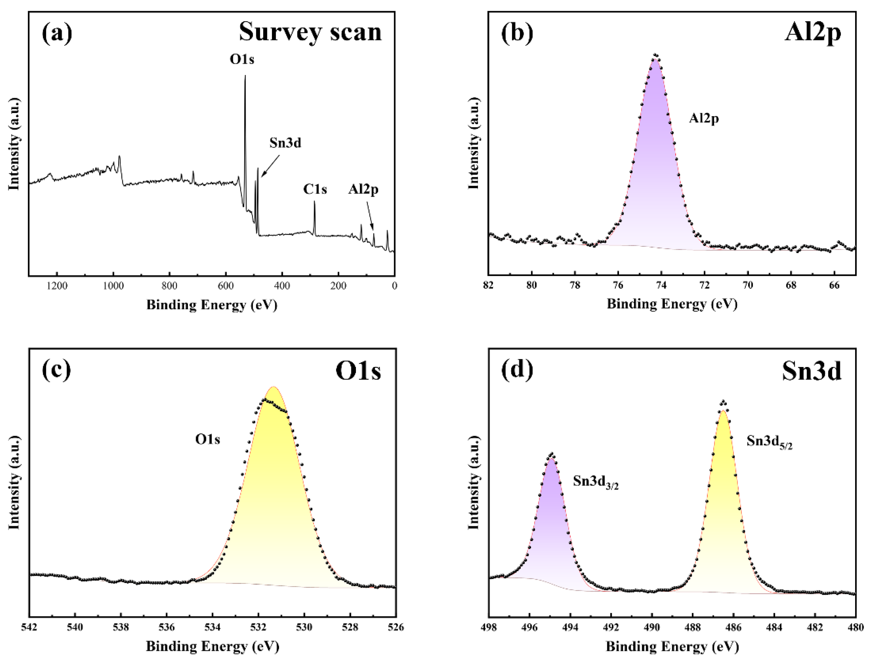
Figure 2 shows the analysis of the XPS spectrum of the sample with an Al doping concentration of 15 at% (A3). Among them, Figure 2a is the full spectrum, Figure 2b is the 2p energy level spectrum of Al, Figure 2c is the 1s energy level spectrum of O, and Figure 2d is the 3d energy level spectrum of Sn. Elements such as C, O, Sn, and Al were successfully detected. Combined with the previous XRD results, it is successfully confirmed that the Al element is incorporated into the SnO2 thin film by replacing the position of Sn4+. From Figure 2d, it can be observed that the 3d energy level of Sn undergoes energy level splitting, which is split into two energy levels, Sn3d5/2 and Sn3d3/2, respectively. The corresponding peak positions are approximately 486 eV and 495 eV. Through calculation, the corresponding splitting distance is approximately 9 eV. This characteristic is consistent with the electron structure characteristics of Sn in SnO2, thus confirming that the sample indeed exists in the form of SnO2 [32].

3.1.3. Analysis of the SEM Results

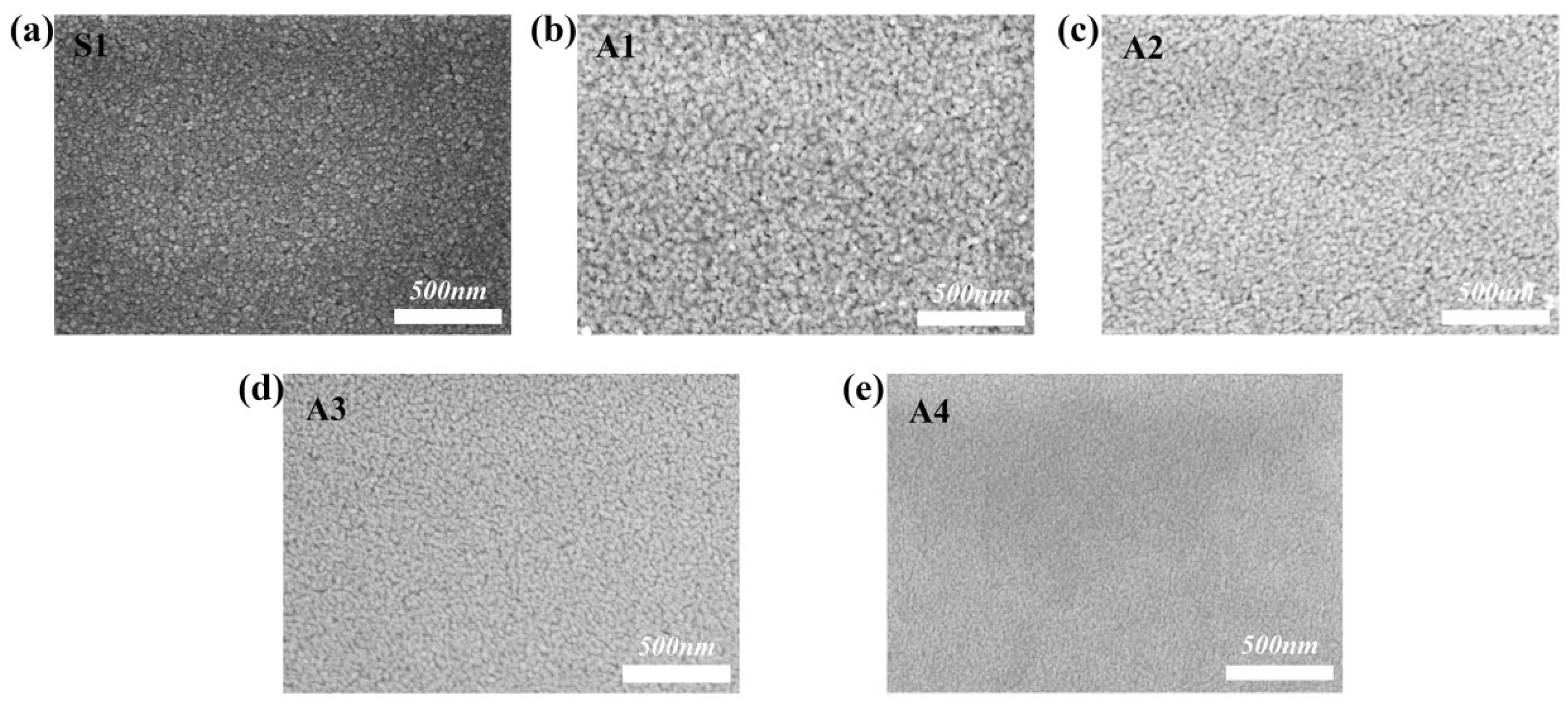
SEM tests were conducted on the intrinsic SnO2 thin films and SnO2 thin films with different Al doping concentrations (A1–A4), and the corresponding test results are shown in Figure 3. It can be clearly and significantly observed that a series of regular changes have occurred in the microstructure of the samples. As the Al doping concentration increases, the grain size of the samples shows a gradual decreasing trend. Moreover, the sample surface becomes increasingly dense. This phenomenon may be attributed to the difference in ionic radii between Al3+ and Sn4+. When Al is introduced as a doping element into the lattice structure of the sample, it causes slight changes in the lattice parameters. As the Al doping amount increases, more Al ions enter the lattice, and the inhibitory effect on crystal growth gradually intensifies.

3.1.4. Analysis of the Optical Properties

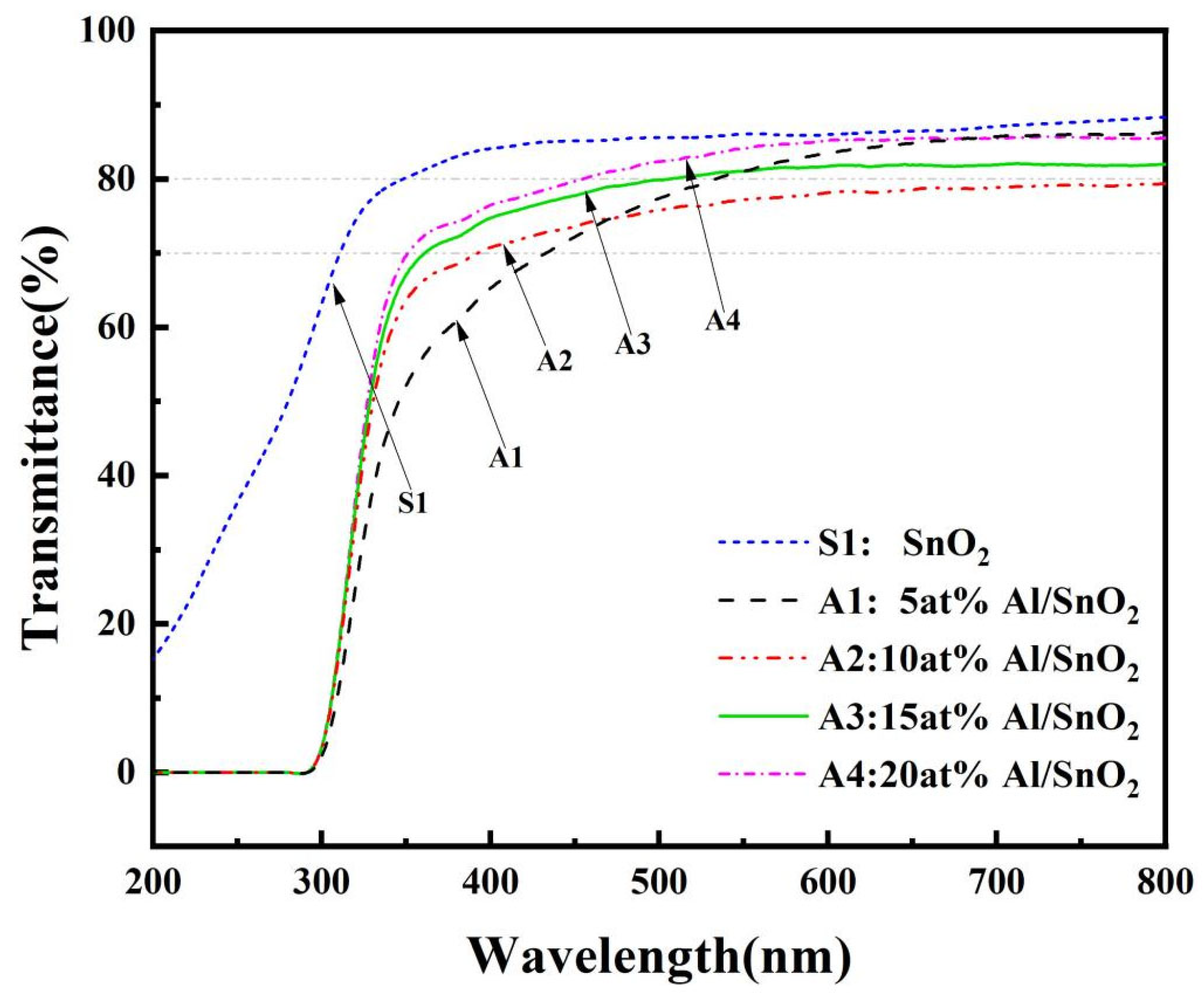
UV-Vis spectral tests were carried out on SnO2 thin film samples with different Al doping concentrations (A1–A4), and the corresponding spectra are shown in Figure 4. According to the results presented in the UV-Vis spectra, compared with the intrinsic sample, the overall transmittance of each doped sample decreased to a certain extent after the incorporation of the Al element. However, it is worth noting that except for the sample with an Al doping concentration of 5 at% (A1), the remaining samples showed a trend that as the Al doping concentration gradually increased, the transmittance also increased. Especially when the Al doping concentration reached 20 at% (A4), its average transmittance in the visible light range could basically reach more than 85%. Although these transmittance values are still slightly lower than those of the intrinsic sample, they are still at a relatively high level as a whole, indicating that the Al-doped thin film still has good light transmittance properties. This phenomenon may be attributed to the introduction of impurity energy levels when Al is doped into SnO2. When the Al doping concentration is 5 at%, in comparison with other doping concentrations, electrons are likely to have a higher probability of transitioning to the conduction band at this moment, resulting in distinct absorption characteristics of ultraviolet light compared to those of samples with other concentrations. When the Al doping concentration increases further, more Al atoms are incorporated into the lattice, increasing the number of impurity energy levels and creating conditions favorable for electron transitions. Consequently, the absorption within the ultraviolet range weakens, and the transmittance increases. Further analysis reveals that the trend of the sample’s transmittance changing with the Al doping concentration shows a good match with the results reflected in the SEM images. Further analysis reveals that the trend of the sample’s transmittance changing with the Al doping concentration shows a good match with the results reflected in the SEM images.
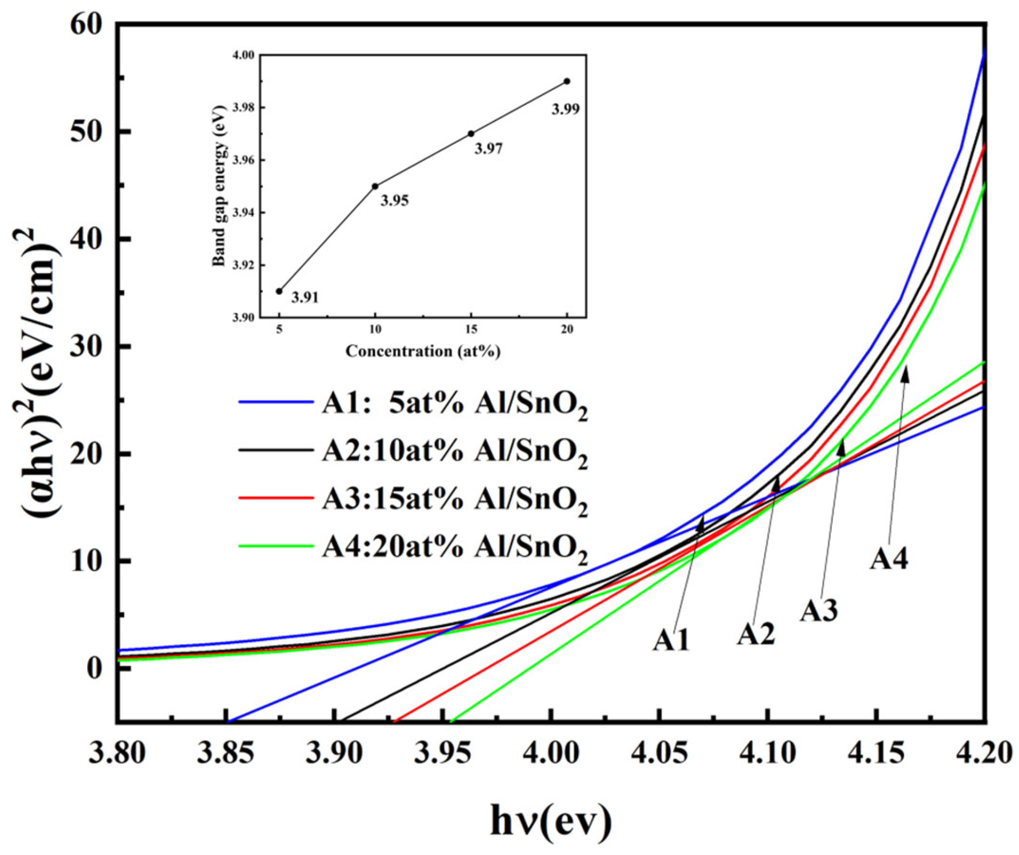
The obtained transmittance data were converted into absorbance data, and the corresponding band-gap width spectra were plotted as shown in Figure 5. The band-gap values of each sample were determined to be 3.91 eV, 3.95 eV, 3.97 eV, and 3.99 eV, respectively. From these data and the spectra, it can be intuitively observed that as the Al doping concentration increases, the band-gap width of the thin film shows a widening trend. This phenomenon is most likely caused by the Burstein–Moss effect, which often affects the band-gap during the semiconductor doping process, changes the electron filling state, and thus broadens the band-gap width.

3.1.5. Analysis of the Electrical Properties

Hall effect tests were carried out on SnO2 thin film samples prepared with different Al doping concentrations, as well as a series of samples including the SnO2 thin film sample (S1) without Al doping. The resistivity, mobility, carrier concentration, and Hall coefficient were measured. The results are listed in Table 1. The test results show that, compared with the undoped thin film sample, the resistivity of all the doped samples after the incorporation of the Al element decreased significantly. This indicates that Al doping has a remarkable effect on reducing the resistivity of SnO2 thin films and can effectively improve their electrical conductivity. However, as the Al doping concentration gradually increases, the resistivity shows a trend of gradually increasing. Only the sample with a doping concentration of 15 at% (A3) has the lowest resistivity. This trend of change suggests that the doping of the Al element can reduce the resistivity to a certain extent, and there exists an optimal doping concentration (15 at%). When the concentration exceeds this value, it may be due to the increase of lattice defects or other microstructural changes caused by excessive Al doping, resulting in an increase in resistivity. When studying SnO2 thin film samples with different Al doping concentrations, it was found that, except for sample A3, the mobility of all the other Al-doped samples is lower than that of the intrinsic sample. However, as the doping concentration gradually increases, the mobility shows a slight increasing trend, and the mobility of sample A3 reaches the maximum value. At the same time, the carrier concentration has been greatly increased after the doping of the Al element. However, with the further increase of the doping concentration, the carrier concentration decreases slightly, and sample A3 exhibits the highest carrier concentration among all the doped samples. Through a comprehensive comparative analysis of these calculation results, it can be seen that the optoelectronic properties of the Al-doped samples have been significantly improved compared with those of the undoped samples. Interestingly, the test results show that when the Al doping concentration reaches more than 15 at%, the semiconductor type of the material changes from an n-type semiconductor to a p-type semiconductor. A thorough analysis of the reasons behind this phenomenon mainly lies in the difference in the outer electron structures of Al and Sn atoms. An Al atom has three electrons in its outermost shell, while a Sn atom has four electrons in its outermost shell. When Al is incorporated into the SnO2 lattice by replacing the position of Sn, for each Al atom incorporated, there will be one less electron compared with a Sn atom, which will then generate an oxygen vacancy. As the amount of Al doping continuously increases, the number of oxygen vacancies also increases. This change in the number of oxygen vacancies ultimately leads to the transformation of the semiconductor type of the material.

3.2. Influence of Sb Doping on the Photoelectric Properties of Al-SnO2 Thin Films

3.2.1. Analysis of the XRD Results

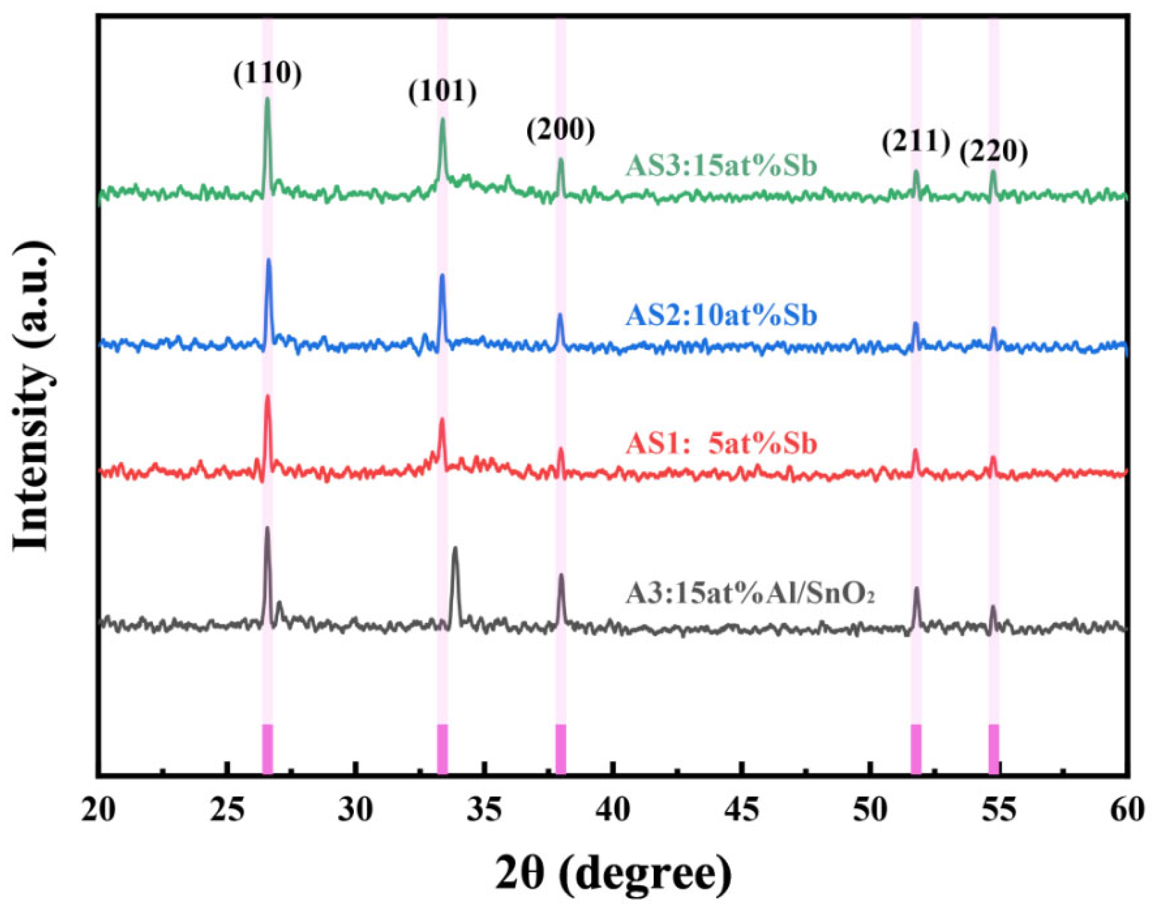
Through a detailed analysis of the XRD pattern (Figure 6), distinct diffraction peaks were detected near the 2θ angular positions of 26.58°, 33.36°, 37.98°, 51.76°, and 54.78°. After precise comparison with the standard card, it is determined that these diffraction peaks correspond to the (110), (101), (200), (211), and (220) crystal faces of the tetranorutile phase of SnO2, respectively, and that the sample is also selectively grown along the (110) crystal faces. From this, it can be inferred that the incorporation of the Sb element did not change the original crystal structure of the sample. It is further confirmed that, similar to the Al element, the Sb element is incorporated into the sample by replacing the position of Sn. Upon further observation of the XRD pattern, it was found that when the Sb doping concentration was low (AS1, AS2), the intensity of the diffraction peaks of the samples was slightly lower compared with that of the single Al-doped sample (A3). However, as the Sb doping concentration continuously increased, after the doping concentration increased to 15 at% (AS3), the intensity of the diffraction peaks exceeded that of the single Al-doped sample, and the overall diffraction peaks were relatively sharp. This phenomenon indicates that under a higher Sb doping concentration, the co-doped system gradually formed a more stable and ordered crystal structure.

3.2.2. Analysis of the XPS Results

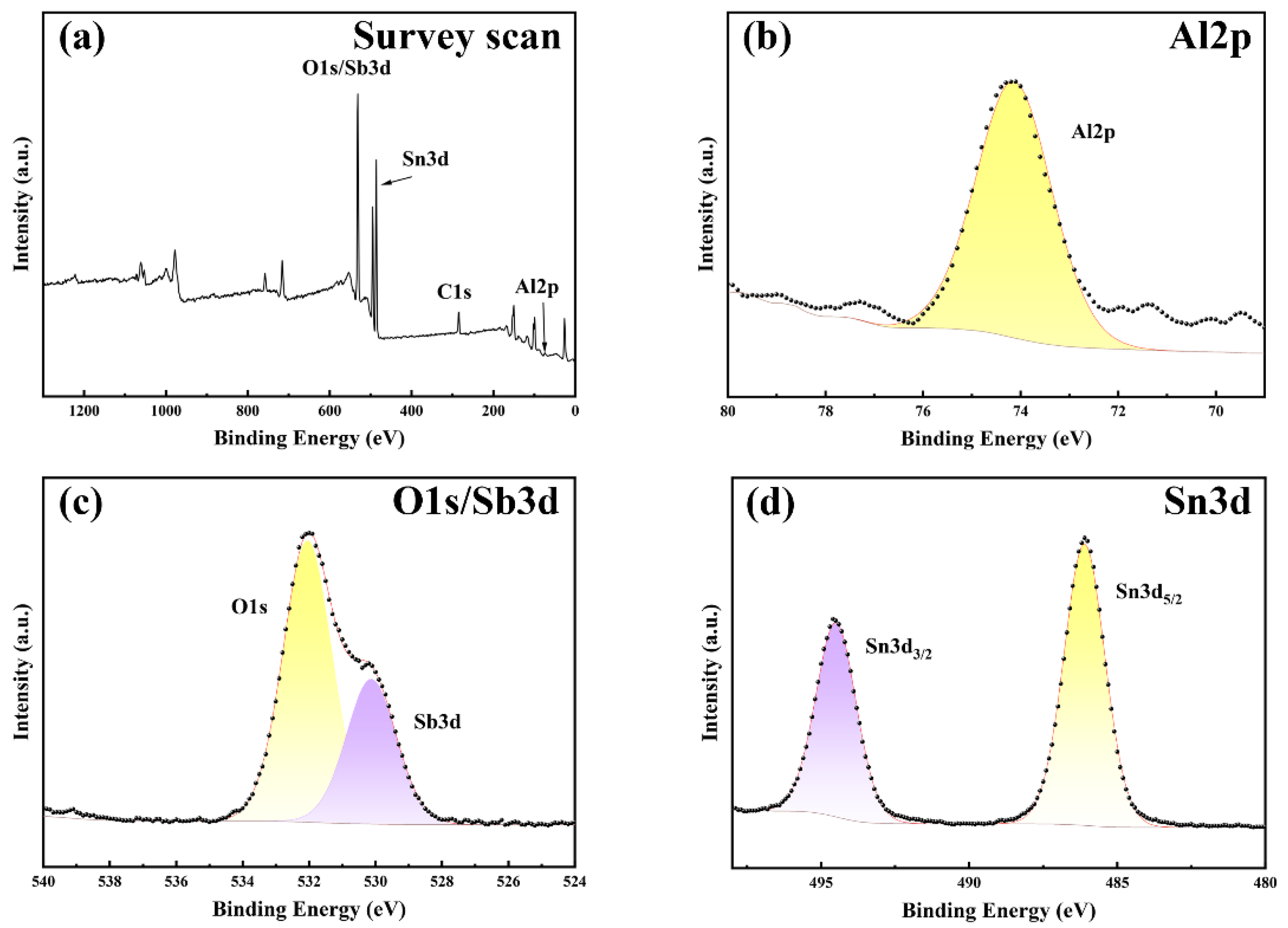
As shown in the XPS spectra presented in Figure 7, it includes the full spectrum (Figure 7a) and the spectra corresponding to different elements, such as Al2p (Figure 7b), O1s/Sb3d (Figure 7c), and Sn3d (Figure 7d). The analysis of the spectral results shows that the presence of elements such as Sn, O, C, Al, and Sb has been successfully detected. Combined with the previous XRD test results, it strongly proves that the Al and Sb elements have been successfully incorporated into the sample, and the incorporation is achieved by replacing the positions of Sn4+ ions. When carefully observing the spectra of each element, it is found that there is a certain overlap between the peak position of Sb3d and that of O1s. For the Sn element, the energy level of Sn3d is observed to split into 3d5/2 and 3d3/2, and their highest peaks appear at 485.1 eV and 493.5 eV, respectively, with a splitting distance of 8.4 eV. This characteristic is consistent with the typical electronic structure characteristics of the Sn element in SnO2, thus further confirming the presence of SnO2 in the sample.

3.2.3. Analysis of the SEM Results

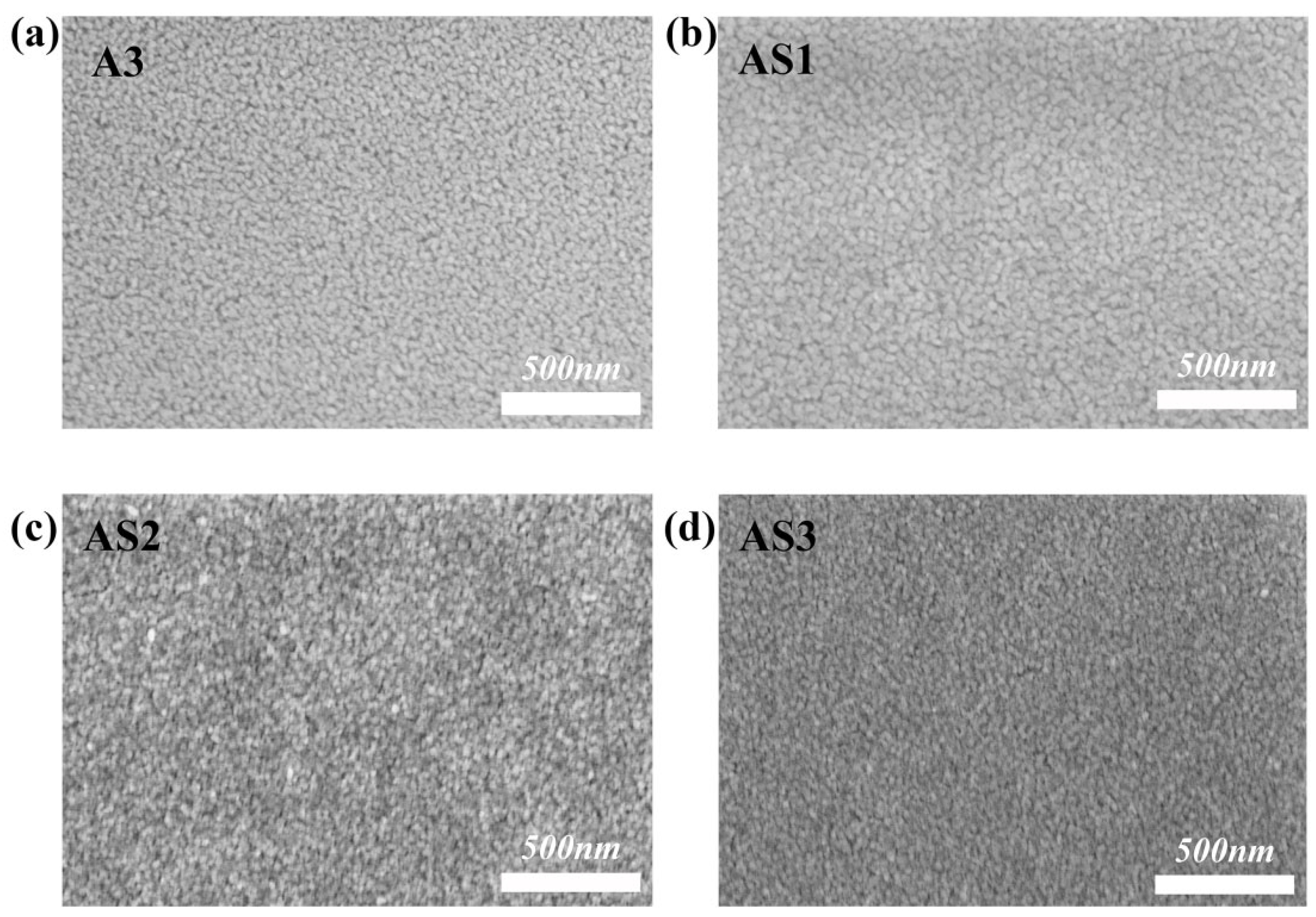
By analyzing the SEM images of Al-Sb co-doped SnO2 thin films prepared with different Sb doping concentrations (AS1–AS3) (as shown in Figure 8, where A3 is the SEM image of the single Al-doped sample), it can be intuitively observed from the SEM images that, compared with the sample doped with only Al element, after further incorporating the Sb element, the grain size shows a tendency to increase. The reason for this may be because the ionic radius of antimony is larger than those of tin ions and aluminum ions. Upon further observation, it is found that, compared with the sample doped with only Al element, the surface quality of the co-doped sample is slightly deteriorated, and there are certain agglomeration and adhesion phenomena. This indicates that when the Sb element is initially incorporated, it may destroy the originally relatively uniform and regular surface structure, resulting in the interference of the orderly arrangement between atoms or particles. As the Sb doping concentration continuously increases, the quality of the surface morphology gradually improves. When the Sb doping concentration increases to 15 at%, there are basically no obvious defects on the surface of the thin film, the overall particles are dense, and the growth is good.

3.2.4. Analysis of the Optical Properties

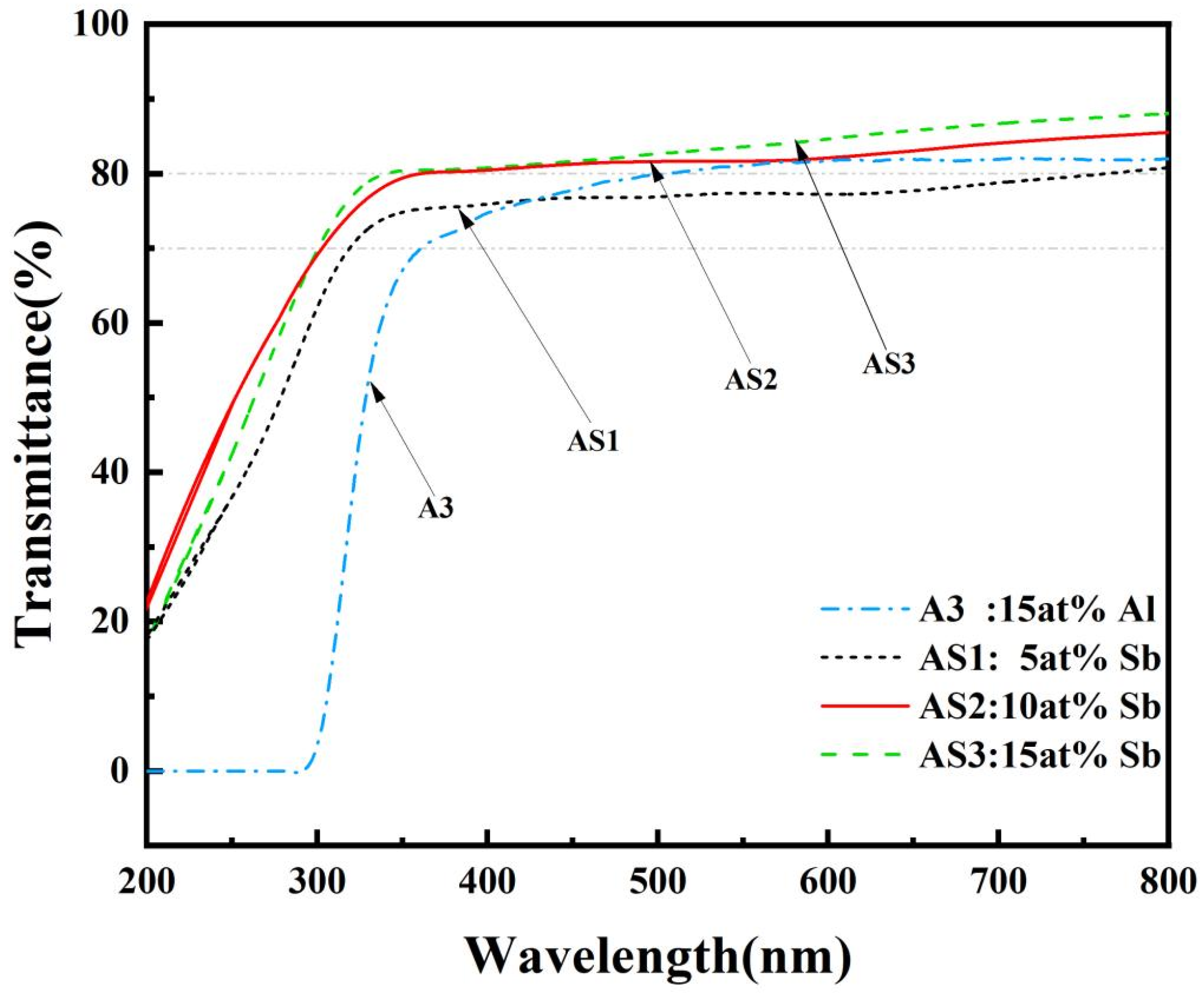
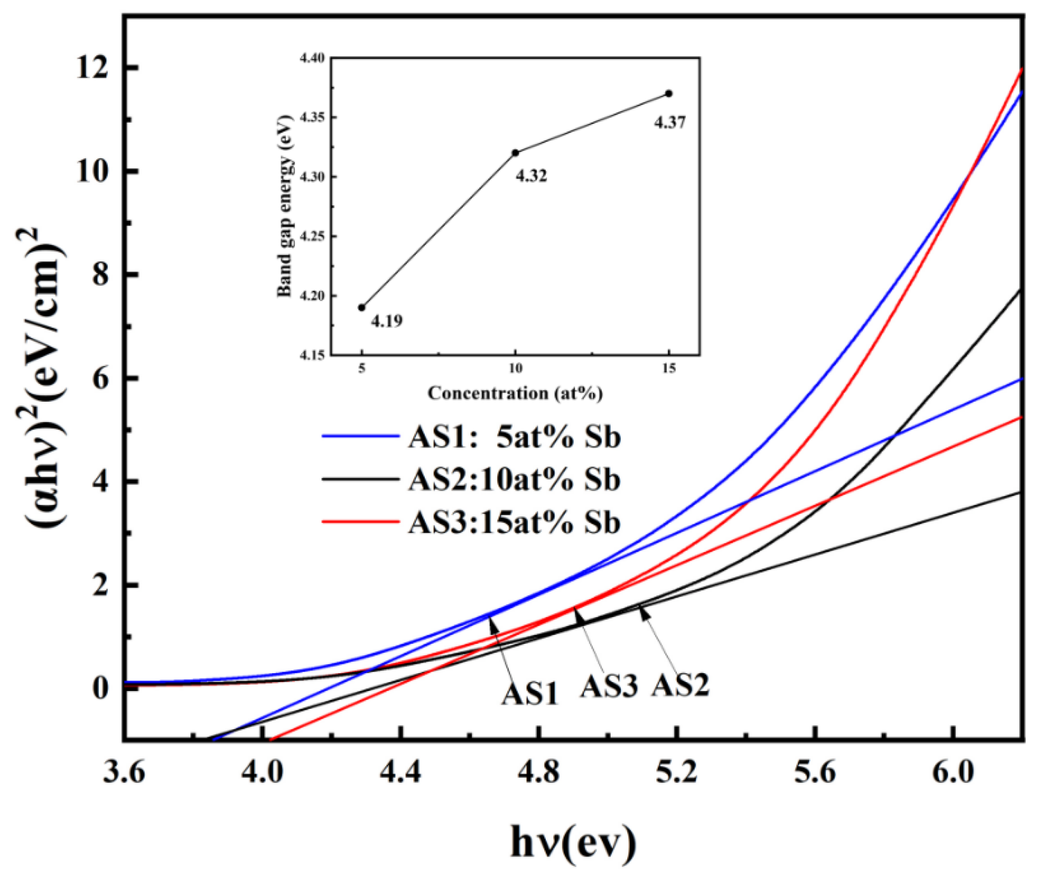
The results of the transmittance test are shown in Figure 9. Only when the Sb doping concentration is low (AS1), the transmittance of the sample is lower than that of the single Al-doped sample (A3). Combined with the results of the SEM test, it is known that the AS1 sample has more surface defects and obvious agglomeration phenomena. This enhances the scattering of light when it propagates in the thin film, thus leading to a decrease in transmittance. As the Sb doping concentration continuously increases, the surface quality of the thin film gradually improves. Correspondingly, the transmittance also keeps increasing. When the Sb doping concentration reaches 15 at%, its average transmittance in the visible light range can reach 84.226%, which is at a relatively high level. This indicates that under a higher Sb doping concentration, the optical transmittance performance of the thin film has been effectively optimized. The transmittance data were converted into absorbance data to plot the bandgap width spectrum (Figure 10). The calculated bandgap values of the AS1–AS3 samples are 4.19 eV, 4.32 eV, and 4.37 eV, respectively. Compared with the intrinsic sample and the single Al-doped sample, the bandgap width is significantly widened.

3.2.5. Analysis of the Electrical Properties

The Hall effect test and analysis were carried out on the prepared samples, and the results are listed in Table 2. The results show that as the Sb doping concentration increases, the resistivity of the thin film shows a continuous decreasing trend. It is highly likely that after the incorporation of Sb, electrons act as the main carriers. Moreover, as the doping concentration gradually increases, the carrier concentration also keeps rising, thus improving the electrical conductivity of the samples. A remarkable phenomenon was also found through observing the test results, that is, the Hall coefficients all became negative after the co-doping of Sb. This indicates that the intrinsic sample changed from an n-type semiconductor to a p-type semiconductor after the incorporation of Al, and then changed back from a p-type semiconductor to an n-type semiconductor after the further incorporation of Sb. This comparative result shows that under different doping conditions, there are differences in the optoelectronic properties of the samples, and the doping elements and their concentrations influence and act synergistically with each other, jointly determining the final performance of the optoelectronic properties.

4. Conclusions

In this study, Al-Sb co-doped SnO2 films were prepared by a simple sol–gel method using SnCl4·5H2O as the Sn source, AlCl3 as the Al source, and SbCl3 as the Sb source. The experimental results show that single Al doping has a significant influence on the photoelectric properties of SnO2 films. When the doping concentration is 15 at%, the crystallization quality is optimal, the band gap value decreases, the resistivity drops, and the carrier concentration increases. There exists a phenomenon of transformation in the conductivity type of semiconductors. The co-doping of Al and Sb slightly increases the resistivity on the basis of maintaining high crystallization quality, and the type of semiconductor changes from P-type back to N-type. These research results provide an important reference basis for further optimizing the photoelectric properties of SnO2 films to meet the application requirements of different optoelectronic devices. The sol–gel method for film preparation still has certain limitations. Although it may be relatively simple and feasible in the laboratory, there is uncertainty regarding the scalability from the laboratory scale to large-scale production. Subsequently, the intrinsic relationship between the doping mechanism and the photoelectric performance can be further studied in depth, the possibilities of more element combination doping can be explored, the preparation process can be optimized, and the performance of the thin film can be further improved.

Author Contributions

Conceptualization, Y.W. and H.Z.; methodology, Y.W. and H.Z.; software, H.Z. and Z.Z.; validation, Y.W., L.W. and X.Z.; formal analysis, X.Z. and Z.Z.; investigation, H.Z.; resources, Y.W.; data curation, Y.W., L.W. and H.Z.; writing—original draft preparation, H.Z.; writing—review and editing, Y.W. and X.Z.; visualization, Y.W.; supervision, Y.W.; project administration, Y.W.; funding acquisition, Y.W. All authors have read and agreed to the published version of the manuscript.

Funding

This research was funded by the Liaoning Provincial Department of Education, grant number LJKMZ20221429.

Institutional Review Board Statement

Not applicable.

Informed Consent Statement

Not applicable.

Data Availability Statement

Data are contained within the article.

Conflicts of Interest

The authors declare no conflicts of interest.

References

  1. Huda, M.N.; Hashmi, G. Fabrication, characterization and performance analysis of sol–gel dip coated SnO2 thin film. Discov. Mater. 2025, 5, 10. [Google Scholar] [CrossRef]
  2. Kania, A.; Szindler, M.M.; Szindler, M.; Brytan, Z.; Łoński, W. Structure and Selected Properties of SnO2 Thin Films. Materials 2024, 17, 3348. [Google Scholar] [CrossRef] [PubMed]
  3. Joseph, D.P.; Radha, R.; Fernandes, J.M.; Muniramaiah, R.; Purushothamreddy, N.; Kovendhan, M.; Venkateswaran, C. Investigation of the transparent conducting properties of spray-pyrolyzed Li and F co-doped SnO2 thin film electrodes. J. Mater. Sci. Mater. Electron. 2022, 33, 8435–8445. [Google Scholar] [CrossRef]
  4. Zhang, Z.; Yin, C.; Yang, L.; Jiang, J.; Guo, Y. Optimizing the gas sensing characteristics of Co-doped SnO2 thin film based hydrogen sensor. J. Alloys Compd. 2019, 785, 819–825. [Google Scholar] [CrossRef]
  5. Fernandes, J.M.; Muniramaiah, R.; Maharana, G.; Janbandhu, S.Y.; Jayavelu, Y.; Kovendhan, M.; Venkateswaran, C.; Sambasivam, S.; Joseph, D.P. Spray-pyrolyzed rare-earth dysprosium-doped SnO2 thin films for plausible photocatalytic application. J. Mater. Sci. Mater. Electron. 2023, 34, 2131. [Google Scholar] [CrossRef]
  6. Nath, A.; Salam, J.A.; Anand, A.M.; Raj, A.; Jayakrishnan, R. Solar cells using spray coated a-axis grown F: SnO2 thin films. Opt. Mater. 2025, 159, 116612. [Google Scholar] [CrossRef]
  7. Rahal, A.; Benramache, S.; Benhaoua, B. Preparation of n-type semiconductor SnO2 thin films. J. Semicond. 2013, 34, 083002. [Google Scholar] [CrossRef]
  8. Bendjedidi, H.; Attaf, A.; Saidi, H.; Aida, M.S.; Semmari, S.; Bouhdjar, A.; Benkhetta, Y. Properties of n-type SnO2 semiconductor prepared by spray ultrasonic technique for photovoltaic applications. J. Semicond. 2015, 36, 123002. [Google Scholar] [CrossRef]
  9. Mokaripoor, E.; Bagheri-Mohagheghi, M.M. Study of structural, electrical and photoconductive properties of F and P co-doped SnO2 transparent semiconducting thin film deposited by spray pyrolysis. Mater. Sci. Semicond. Process. 2015, 30, 400–405. [Google Scholar] [CrossRef]
  10. Tran, Q.P.; Fang, J.S.; Chin, T.S. Properties of fluorine-doped SnO2 thin films by a green sol–gel method. Mater. Sci. Semicond. Process. 2015, 40, 664–669. [Google Scholar] [CrossRef]
  11. Niu, Y.; Duan, L.; Zhao, X.; Han, C.; Guo, J.; Geng, W. Effect of Sb doping on structural and photoelectric properties of SnO2 thin films. J. Mater. Sci. Mater. Electron. 2020, 31, 3289–3302. [Google Scholar] [CrossRef]
  12. Zhang, X.; Liu, X.; Ning, H.; Yuan, W.; Deng, Y.; Zhang, X.; Wang, S.; Wang, J.; Yao, R.; Peng, J. Characterization studies of the structure and properties of Zr-doped SnO2 thin films by spin-coating technique. Superlattices Microstruct. 2018, 123, 330–337. [Google Scholar] [CrossRef]
  13. Soumya, S.S.; Xavier, T.S. Effect of cobalt doping on the microstructural, optical and electrical properties of SnO2 thin films by sol-gel spin coating technique. Phys. B Condens. Matter 2022, 624, 413432. [Google Scholar] [CrossRef]
  14. Sujatha Lekshmy, S.; Joy, K. Structural and optoelectronic properties of indium doped SnO2 thin films deposited by sol gel technique. J. Mater. Sci. Mater. Electron. 2014, 25, 1664–1672. [Google Scholar] [CrossRef]
  15. Che, L.; Song, J.; Yang, J.; Chen, X.; Li, J.; Zhang, N.; Yang, S.; Wang, Y. Fluorine, chlorine, and gallium co-doped zinc oxide transparent conductive films fabricated using the sol-gel spin method. J. Mater. 2023, 9, 745–753. [Google Scholar] [CrossRef]
  16. Houaidji, N.; Ajili, M.; Chouial, B.; Kamoun, N.T. First investigation of structural and optoelectronic properties of F and Ni co-doped SnO2 sprayed thin films. Optik 2020, 208, 164026. [Google Scholar] [CrossRef]
  17. Turgut, G.; Keskenler, E.F.; Aydın, S.; Yılmaz, M.; Doğan, S.; Düzgün, B. An investigation of the Nb doping effect on structural, morphological, electrical and optical properties of spray deposited F doped SnO2 films. Phys. Scr. 2013, 87, 035602. [Google Scholar] [CrossRef]
  18. Abed, C.; Fernández, S.; Aouida, S.; Elhouichet, H.; Priego, F.; Castro, Y.; Gómez-Mancebo, M.B.; Munuera, C. Processing and Study of Optical and Electrical Properties of (Mg, Al) Co-Doped ZnO Thin Films Prepared by RF Magnetron Sputtering for Photovoltaic Application. Materials 2020, 13, 2146. [Google Scholar] [CrossRef]
  19. Guo, Y.; Wang, G.; Huang, R.; Wang, J. Study on Electrical and Optical Properties of Sb-Doped SnO2 Transparent Conducting Films. J. Inorg. Mater. 2002, 132–138. [Google Scholar]
  20. Ramarajan, R.; Kovendhan, M.; Thangaraju, K.; Joseph, D.P.; Babu, R.R.; Elumalai, V. Enhanced optical transparency and electrical conductivity of Ba and Sb co-doped SnO2 thin films. J. Alloys Compd. 2020, 823, 153709. [Google Scholar] [CrossRef]
  21. Rossnagel, S.M. Magnetron sputtering. J. Vac. Sci. Technol. A 2020, 38, 060805. [Google Scholar] [CrossRef]
  22. Leng, D.; Wu, L.; Jiang, H.; Zhao, Y.; Zhang, J.; Li, W.; Feng, L. Preparation and Properties of SnO2 Film Deposited by Magnetron Sputtering. Int. J. Photoenergy 2012, 2012, 235971. [Google Scholar] [CrossRef]
  23. Vernardou, D. Advances in chemical vapor deposition. Materials 2020, 13, 4167. [Google Scholar] [CrossRef]
  24. Yang, J.; Liu, W.; Dong, L.; Li, Y.; Li, C.; Zhao, H. Studies on the structural and electrical properties of F-doped SnO2 film prepared by APCVD. Appl. Surf. Sci. 2011, 257, 10499–10502. [Google Scholar] [CrossRef]
  25. Faudoa-Arzate, A.; Morales-Rodriguez, H.; Sanchez-Carrillo, M.; González-Vázquez, A.; Realyvazquez-Guevara, P.; Rojas, J.; Chávez-Montes, W. SEM Study of Growth of SnO2 Nanoflowers in Thin films by Spray Pyrolysis. Microsc. Microanal. 2019, 25, 840–841. [Google Scholar] [CrossRef]
  26. Soussi, L.; Garmim, T.; Karzazi, O.; Rmili, A.; El Bachiri, A.; Louardi, A.; Erguig, H. Effect of (Co, Fe, Ni) doping on structural, optical and electrical properties of sprayed SnO2 thin film. Surf. Interfaces 2020, 19, 100467. [Google Scholar] [CrossRef]
  27. Deyu, G.K.; Muñoz-Rojas, D.; Rapenne, L.; Deschanvres, J.-L.; Klein, A.; Jiménez, C.; Bellet, D. SnO2 Films Deposited by Ultrasonic Spray Pyrolysis: Influence of Al Incorporation on the Properties. Molecules 2019, 24, 2797. [Google Scholar] [CrossRef]
  28. Kumar, S. Exploration of structural, morphological and magnetic properties of transition metal doped SnO2 films grown using pulsed laser deposition. Vacuum 2020, 182, 109725. [Google Scholar] [CrossRef]
  29. Sinha, S.K.; Ray, S.K.; Manna, I. Effect of Al doping on structural, optical and electrical properties of SnO2 thin films synthesized by pulsed laser deposition. Philos. Mag. 2014, 94, 3507–3521. [Google Scholar] [CrossRef]
  30. Haya, S.; Brahmia, O.; Halimi, O.; Sebais, M.; Boudine, B. Sol–gel synthesis of Sr-doped SnO2 thin films and their photocatalytic properties. Mater. Res. Express 2017, 4, 106406. [Google Scholar] [CrossRef]
  31. Turan, E.; Kul, M.; Akın, S. Structural and optical investigation of spray-deposited SnO2 thin films. J. Mater. Sci. Mater. Electron. 2022, 33, 15689–15703. [Google Scholar] [CrossRef]
  32. Lee, C.; Lee, W.-Y.; Lee, H.; Ha, S.; Bae, J.-H.; Kang, I.-M.; Kang, H.; Kim, K.; Jang, J. Sol-gel processed yttrium-doped SnO2 thin film transistors. Electronics 2020, 9, 254. [Google Scholar] [CrossRef]
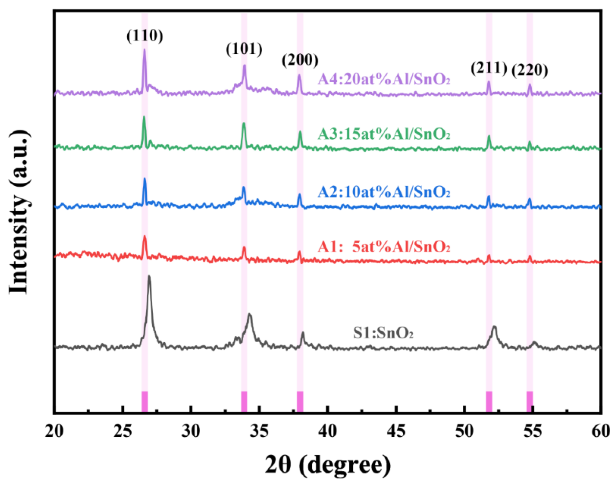
Figure 1. XRD patterns of SnO2 thin films with different Al doping concentrations.
Coatings 15 00669 g001
Figure 2. XPS images of SnO2 thin film samples with a doping concentration of 15at%. (a) XPS full spectrum; (b) Al 2p peak; (c) O 1s peak; (d) Sn 3d5/2 and Sn 3d3/2 peaks.
Coatings 15 00669 g002
Figure 3. SEM of SnO2 thin film samples with different Al doping concentrations. (a) Undoped; (b) 5 at%; (c) 10 at%; (d) 15 at%; (e) 20 at%.
Coatings 15 00669 g003
Figure 4. Transmittance spectra of SnO2 thin film samples with different Al doping concentrations.
Coatings 15 00669 g004
Figure 5. Optical band gap spectra of SnO2 thin film samples with different Al doping concentrations.
Coatings 15 00669 g005
Figure 6. XRD diagram of Al-Sb co-doping SnO2 thin film samples with different Sb doping concentrations.
Coatings 15 00669 g006
Figure 7. XPS diagram of Al-Sb co-doping SnO2 thin film samples. (a) XPS full spectrum; (b) Al 2p peak; (c) O 1s and Sb 3d peaks; (d) Sn 3d5/2 and Sn 3d3/2 peaks.
Coatings 15 00669 g007
Figure 8. SEM of Al-Sb co-doping SnO2 thin film samples with different Sb doping concentrations. (a) 15 at% Al; (b) 5 at% Sb; (c) 10 at% Sb; (d) 15 at% Sb.
Coatings 15 00669 g008
Figure 9. Transmittance spectra of Al-Sb co-doping SnO2 thin film samples with different Sb doping concentrations.
Coatings 15 00669 g009
Figure 10. Optical band gap spectra of Al-Sb co-doping SnO2 thin film samples with different Sb doping concentrations.
Coatings 15 00669 g010
Table 1. Hall measurement data of SnO2 samples with different Al doping concentrations.
Sample NameResistivity (Ω·cm)Mobility (cm2/V·S)Carrier Concentration (cm−3)Hall Coefficient
S1 6.806 × 10−38.753 × 1021.049 × 1019−5.957 × 10⁻²
A1 1.610 × 10−44.205 × 1029.232 × 1019−6.770 × 10⁻²
A2 2.785 × 10−45.354 × 1028.657 × 1019−3.770 × 10⁻²
A3 1.058 × 10−41.085 × 1035.855 × 10201.070 × 10−3
A4 3.581 × 10−46.205 × 1027.813 × 10192.223 × 10−2
Table 2. Hall measurement data of Al-Sb co-doping SnO2 samples with different Sb doping concentrations.
Sample NameResistivity (Ω·cm)Mobility (cm2/V·S)Carrier Concentration (cm−3)Hall Coefficient
A3 1.058 × 10−41.085 × 1035.855 × 10201.070 × 10−3
AS1 2.701 × 10−47.199 × 1024.234 × 1019−1.476 × 10⁻²
AS2 2.653 × 10−46.951 × 1025.389 × 1019−1.844 × 10⁻²
AS3 1.953 × 10−45.465 × 1026.455 × 1020−4.295 × 10⁻²
Disclaimer/Publisher’s Note: The statements, opinions and data contained in all publications are solely those of the individual author(s) and contributor(s) and not of MDPI and/or the editor(s). MDPI and/or the editor(s) disclaim responsibility for any injury to people or property resulting from any ideas, methods, instructions or products referred to in the content.