Article

Structural, Optical and Electrical Properties of the Flexible, Asymmetric TiO2/Cu/Ag/ZnS and ZnS/Cu/Ag/TiO2 Films Deposited via Magnetron Sputtering

1
School of Materials Science and Engineering, Henan Institute of Technology, Xinxiang 453003, China
2
Engineering Research Center for Metallic Materials Modification Technology of Henan Province, Henan Institute of Technology, Xinxiang 453003, China
3
Henan Key Laboratory of Advanced Cable Materials and Intelligent Manufacturing, Henan Institute of Technology, Xinxiang 453003, China
4
National Materials Corrosion and Protection Scientific Data Center, University of Science and Technology Beijing, Beijing 100083, China
*
Author to whom correspondence should be addressed.
Coatings 2025, 15(6), 650; https://doi.org/10.3390/coatings15060650
Submission received: 10 May 2025 / Revised: 24 May 2025 / Accepted: 27 May 2025 / Published: 28 May 2025
(This article belongs to the Section Thin Films)

Abstract

The structural, optical and electrical properties of the flexible, asymmetric TiO2/Cu/Ag/ZnS and ZnS/Cu/Ag/TiO2 transparent conductive films (TCFs) were studied. The multilayered TCFs were magnetron sputtered onto the flexible PET substrate layer-wise, with TiO2, ZnS, Cu and Ag targets. The atomic force microscope, scanning electronic microscope, X-ray diffractometer, ultraviolet-visible spectrophotometer and four-probe tester were utilized to characterize the samples. The photoelectric property of the multilayers varies with the adjustment in structural parameters. The ZnS/Cu/Ag/TiO2 samples demonstrate a more uniform surface morphology and better optical and electrical properties than the TiO2/Cu/Ag/ZnS counterparts. The optimal sheet resistance and average transmittance of the ZnS/Cu/Ag/TiO2 films are 5.56 Ω/sq and 88.46% in the visible spectrum, with the corresponding figure of merit reaching 52.76 × 10⁻³ Ω−1. The bottom ZnS layer reveals superior percolation function for the bimetallic layer, forming with good continuity and homogeneity, although the original surface roughness is higher than that of TiO2. The top TiO2 layer demonstrates a smooth morphology and dense structure, beneficial to the high transparency and stability of the multilayer.

1. Introduction

Transparent conductive films (TCFs) have been utilized as an essential photoelectric material in extensive applications like photovoltaic systems, flat-panel displays, light-emitting diodes, electromagnetic interference shielding windows and low-emissivity glasses [1,2,3]. The recent advancements in flexible electronics have broadened the implementation scope of TCFs [4,5,6,7]. Currently, transparent conductive oxides (TCOs), especially indium tin oxide (ITO), dominate the industrial applications of TCFs due to their balanced performance characteristics [4,8]. Nevertheless, due to the inherent limitation in the electrical conductivity and mechanical flexibility of TCOs, composite TCFs have been prompted, incorporating highly conductive materials such as silver nanowires, carbon nanotubes, graphene, metallic grids or ultrathin metal films (UTMs). Notably, multilayered TCFs employing a UTM as the intermediate layer demonstrate superior optical and electrical performances, enhanced mechanical flexibility and customizable design parameters [4,9]. Moreover, its fabrication process is highly compatible with industrial-scale roll-to-roll (RTR) production techniques [10].
Multilayered TCFs typically employ a dielectric/metal/dielectric (DMD) structure, where the metallic layer serves as the primary contributor to electrical conductivity and exceptional mechanical resilience [7,8,11]. The dielectric layers can effectively suppress light reflection and mitigates the surface plasmon resonance (SPR) effects at the metal/dielectric boundaries [12,13,14], acquiring good light transmission performance for the multilayers. The top dielectric layer could also work as an environmental barrier against corrosive agents, improving the stability of the film [15].
The metallic layers in multilayered TCFs should possess high electrical conductivity and low extinction coefficients, with material selections encompassing pure metals (e.g., Ag, Au, Cu, Al and Mo), alloys or bimetals, revealing a typical thickness range of 6–14 nm [1,9,16,17,18]. While the transmittance of metallic films generally decreases with an increasing thickness, excessively thin layers fail to meet the high electric conductivity requirement. Ag maintains the most popular intermediate-layer material due to its superior conductivity among metals and relatively low optical absorption coefficients in the visible spectrum, although a few studies have reported alternative metallic options [1,19]. Furthermore, seed layers (e.g., Cu [20,21], Al [21,22] and Ti [23,24]) can be utilized to enhance the uniform nucleation of metallic layers and lower the critical film-forming thickness.
The dielectric layers in a multilayered TCF should exhibit high refractive indices and low extinction coefficients within the visible spectrum [3,20]. These layers may employ either TCOs or non-conductive transparent oxides/sulfides (e.g., In₂O₃, ZnO, TiO₂ and ZnS), depending on specific device encapsulation requirements [3,4]. The top and bottom dielectric layers may utilize identical or distinct materials, corresponding to symmetric [1,3,25] or asymmetric [19,26,27] structures. Optimal thickness design can enhance the optical transparency, and the material selection enables precise tuning of the TCF’s work function to meet specific requirements.
The substrate selection for flexible TCFs normally includes transparent polymer films [16,18,28] such as polyethylene terephthalate (PET) and polyethylene naphtholate (PEN) or flexible glass [17]. Polymer films offer advantages including low cost, excellent bending resistance and high optical transparency, making them a popular choice for flexible optoelectronic devices. However, these materials exhibit limited thermal stability, with typical tolerable temperatures below 150 °C, necessitating low-temperature deposition techniques and precluding the use of conventional annealing processes [1].
The flexible, asymmetric TiO2/Cu/Ag/ZnS and ZnS/Cu/Ag/TiO₂ multilayered TCFs are studied in this paper. These architectural configurations for TCFs have rarely been reported. The design capitalizes on the enhancement effect of the Cu seed layer on the intermediate layer’s film-forming process, combined with the favorable processing property and optoelectronic performance of ZnS and TiO₂ dielectric materials, aiming to explore the synergistic effects of sublayers in the asymmetric, multilayered TCFs.

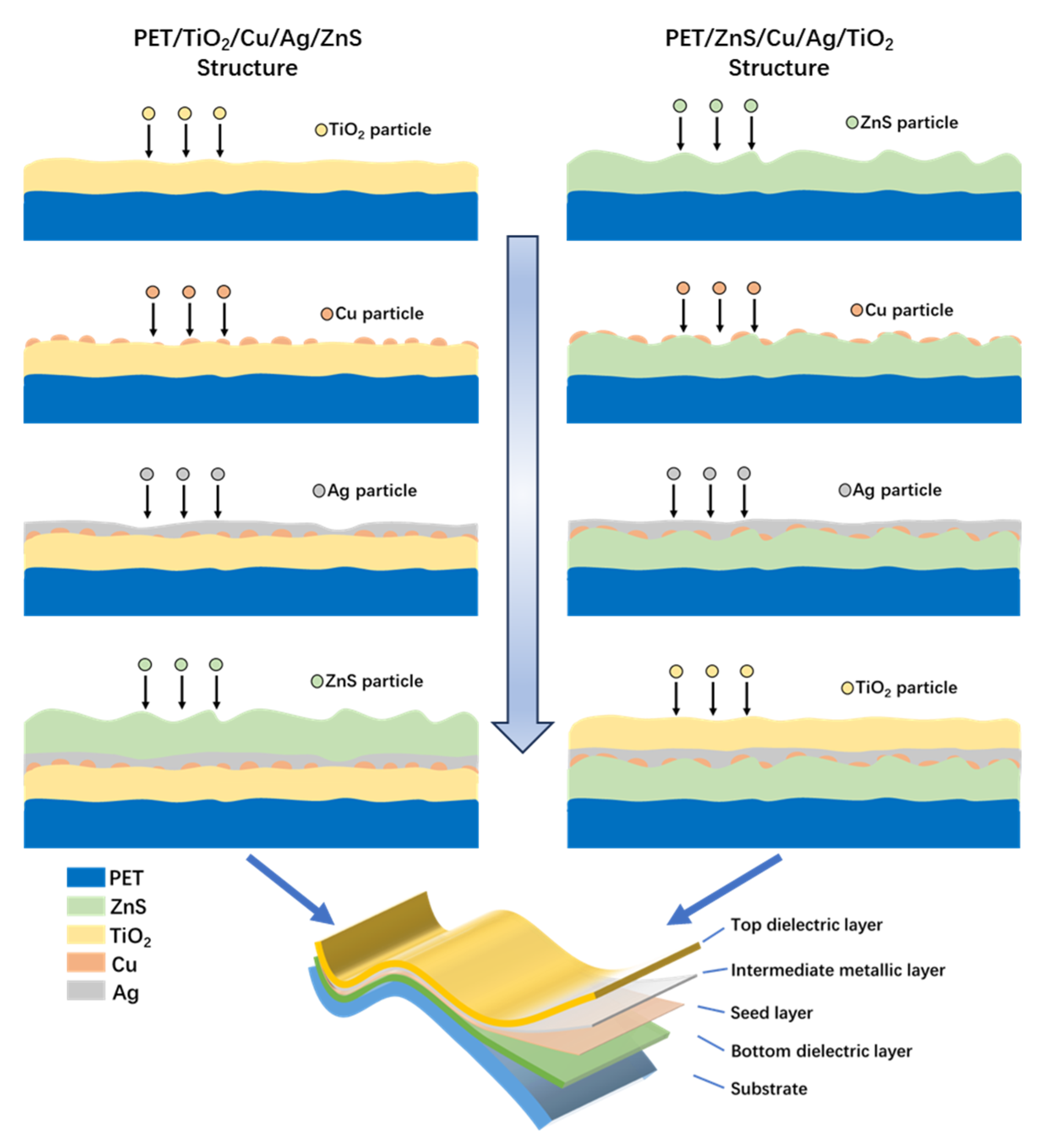
2. Materials and Methods

The Ag and Cu sputtering targets (76.2 mm diameter, ≥99.99% purity, from ZhongNuo Advanced Material (Beijing) Technology Co., Ltd., Beiing, China) were adopted for metallic interlayers, while the TiO₂ and ZnS targets were utilized for dielectric layer deposition. Prior to the sputtering process, the flexible PET sheet substrates (0.175 mm thickness, 20 mm × 20 mm planar dimensions, from South China Xiangcheng Technology Co., Ltd., Shenzhen, China) underwent sequential ultrasonic cleaning in acetone and anhydrous ethanol (10 min each, from Xilong Scientific Co., Ltd., Shanghai, China), followed by deionized water (home made in the laboratory) rinsing and high-purity N₂ (from Yuanzheng Special Gas Co., Ltd., Xinxiang, China) drying.
The multilayered films were fabricated using a JSD-500 four-target magnetron sputtering system (Jiashuo Vacuum Technology Co., Ltd., Hefei, China). The TiO₂ and ZnS dielectric layers were deposited via radio frequency (RF) sputtering at 150 W and 50 W, respectively. The metallic interlayers were sputtered using direct-current (DC) power sources at 10 W for Cu and 120 W for Ag, with a fixed 90 mm target-substrate distance. A base pressure of 5 × 10⁻⁴ Pa was established prior to introducing 70 sccm Ar gas (≥99.99% purity), maintaining the chamber pressure at 0.4 Pa via baffle valve adjustment. During the deposition process, sequential sublayer deposition occurred without substrate heating, and the thickness was controlled via the deposition time under stabilized parameters. The deposition rate for each material was pre-calibrated by measuring the thickness versus time from a thicker film under identical deposition parameters. The nominal thickness for ultrathin Cu layers (<1 nm) with discontinuous island structures corresponds to an equivalent thickness.
The layer morphology was characterized via field-emission scanning electron microscopy (FE-SEM, Hitachi SU8010, Tokyo, Japan) with energy-dispersive X-ray spectroscopy (EDS, Bruker Quantax300-30, Boston, MA, USA). The quantitative analysis of the images was conducted using the software ImageJ (version 1.53K, by National Institutes of Health, Bethesda, MD, USA). Atomic force microscopy (AFM, Bruker Dimension Icon, Boston, MA, USA) was utilized for the surface features of the non-conductive films. The phase structures were determined via grazing-incidence X-ray diffraction (GIXRD, Rigaku SmartLab 3 kw, Tokyo, Japan) at a scanning rate of 2°/min. The optical transmittances of the film samples were measured via UV-Vis spectrophotometry (Youke UV756, Shanghai, China), with the average transmittance ( T a v ) calculated as Equation (1):
T a v = 1 n i = 1 n T i
where T i denotes the transmittance at specific wavelengths, and n represents data points of the defined spectrum. The electrical properties were evaluated via four-point probe (JG M-3, Suzhou, China) measurements, and the thickness quantification was conducted via non-contact 3D profilometry (Rtec R-wlafm, San Jose, CA, USA) and spectroscopic ellipsometry (Horiba SAS, Shanghai, China).

3. Results

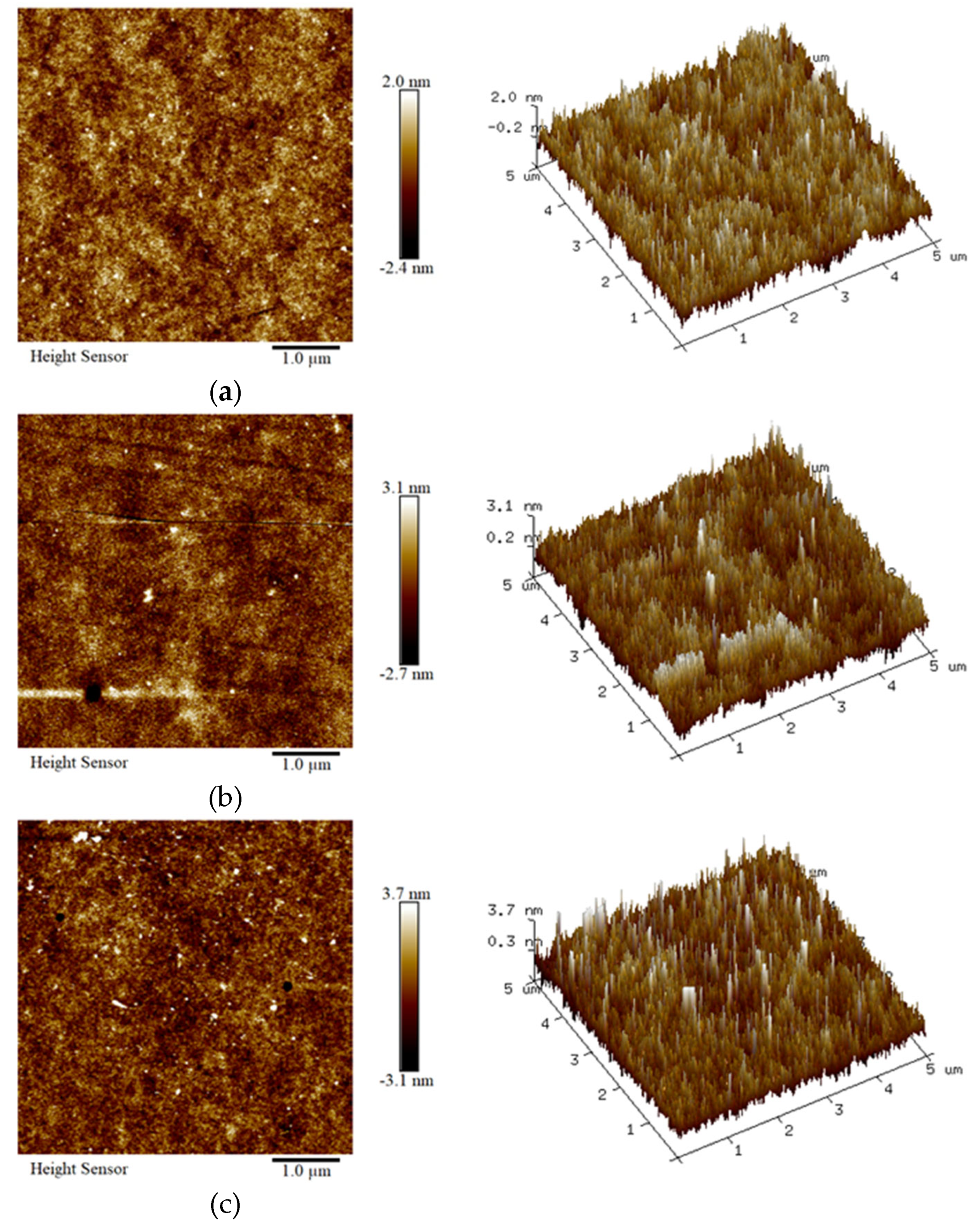
3.1. Surface Characterization of the Substrate and Bottom Dielectric Layers

The surface features of the PET substrate and bottom dielectric layers were analyzed using atomic force microscopy (AFM), which is suitable for non-conductive materials. Figure 1 presents the planar and three-dimensional AFM topographies. The pristine PET substrate demonstrates a uniform surface morphology (Figure 1a) with surface roughness of R a 0.441 nm, which is in the preferred roughness range of TCF substrates (Ra < 1 nm) [26].
The D/M/D-structured TCFs were fabricated through layer-wise deposition. The deposition of the bottom dielectric layer (36 nm TiO2 or 41 nm ZnS) induced morphological evolution dependent on the material selection and sputtering parameters. AFM images reveal homogeneous surface features for both dielectric materials, as shown in Figure 1b,c, with roughness values of R a 0.630 nm for TiO2 and R a 0.685 nm for ZnS. These results indicate a marginal amplification of surface roughness compared to the bare substrate.

3.2. Surface Morphology of the Intermediate Layers and Top Dielectric Layers

The surface morphology of the intermediate metallic layers and top dielectric layers was analyzed utilizing FE-SEM. A TiO2/Ag structure was fabricated via sequential sputtering-deposition of a 36 nm TiO2 layer and 9.5 nm Ag layer on the PET substrate, and the image is shown in Figure 2a. The Ag layer with a light contrast exhibits a heterogeneous morphology across the bottom TiO2 surface (dark contrast). Some particles with a relatively big size range of 47–83 nm in diameter are distributed in the matrix layer. The Ag sublayer is not completely continuous, with a coverage rate of 98.1%. The continuity of the metallic layer was significantly improved by introducing an ultrathin 0.25 nm Cu seed layer between the sublayers of TiO2 and Ag, corresponding to a TiO2/Cu/Ag structure. As displayed in Figure 2b, the bimetallic layer reveals a near-full coverage (99.8%) with sparse vacancies. The surface smoothness is much enhanced with uniform distribution of very fine particles. This phenomenon confirms the seed layer’s role in promoting the continuous film formation and can be explained in terms of the bond dissociation energies (H, enthalpy, HAg-Ag = 163 kJ∙mol−1 and HAg-Cu = 176 kJ∙mol−1) [23]. The sputtered Ag atom favors bonding with the deposited Cu atom, giving rise to a more uniform state.
The top dielectric layer of the 41 nm ZnS layer was further deposited onto the TiO2/Cu/Ag film, achieving a complete D/M/D structure of TiO2/Cu/Ag/ZnS. The morphology of the top ZnS layer, as presented in Figure 2c, is uniform and completely continuous, with no vacancy. The smooth surface is composed of small particles of a narrow size distribution, with an average diameter of around 30 nm.
When the bottom layer material was changed from TiO2 to ZnS, the metallic layers deposited afterward exhibited obvious variations. The surface of the ZnS/Ag bilayer structure, with sublayer thicknesses of 41 nm and 9.5 nm, respectively, appears as a heterogeneous morphology, as shown in Figure 2d. The Ag layer (light contrast) is partially continuous due to a few vacancies of irregular shape. There are more bigger particles with a size range of 59–150 nm, and the surface roughness increases compared with the TiO2/Ag structure. The corresponding coverage rate is 91.8%, which means a worse percolation property compared with the case in Figure 2a. Considering that the ZnS layer possesses superior percolating [11] or wetting [23,29] performance among popular dielectric layers of different materials, the decaying performance of ZnS should be attributed to the higher surface roughness [26] under preparation conditions. The adoption of 0.25 nm Cu seed layer to the ZnS/Ag structure resulted in tremendous progress in the integrity, uniformity and smoothness of the metallic layer, corresponding to the ZnS/Cu/Ag structure, as presented in Figure 2e. The homogeneous bimetallic layer demonstrates perfect continuity, with only a sporadic distribution of relatively large particles with a typical size of around 50 nm. It seems that the ZnS layer is more functional in the seed layer promotion effect on film formation than TiO2. A preferred topographic feature of metallic layer is then obtained on the ZnS bottom layer despite its higher surface roughness. A TiO2 layer of 36 nm thickness was further sputtered-deposited as the top dielectric layer, forming the ZnS/Cu/Ag/TiO2 structure. As displayed in Figure 2f, the morphology of the TiO2 layer is uniform and completely continuous, appearing smoother and consisting of smaller particles than the ZnS layer (Figure 2c), with a typical diameter size of about 38 nm.

3.3. Phase Structure Analysis for the TiO2/Cu/Ag/ZnS Multilayer

The phase structures were analyzed via XRD for the multilayered TCF of TiO2/Cu/Ag/ZnS. Considering the small thickness of the sublayers, the GIXRD technique was utilized to better reveal the characteristic information of the surface-adjacent zone. An optimized grazing incidence angle of 1° was selected from the angle range of 0.2–1.5°. A deliberately larger thickness of 40 nm was adopted for each sublayer in the TCF to further enhance the effective diffraction signals. The corresponding structure of 40 nm TiO2, 40 nm Cu, 40 nm Ag and 40 nm ZnS is abbreviated as Z40 C40 A40 T40 (the same abbreviation rule remains in the rest of the paper). This sample was fabricated under the identical process parameters via magnetron sputtering, and the test result is illustrated in Figure 3, where the prime diffraction peaks are labeled according to the standard phase data (ICSD #67994, #64699 and #60378). The strongest peak set is from the Ag layer, and another distinct peak set was calibrated from the Cu layer. Furthermore, one weak peak at the lower diffraction angle was distinguished from the ZnS phase. However, no clear peak was found related to the TiO2. It seems that the metallic layers possess better crystallization than the dielectric layers according to the GIXRD results. Under the magnetron sputtering process here without external heating, the crystallization process should complete partially in the ZnS layer [19,29], leading to the fuzzy peak profile, whereas the TiO2 phase remains virtually amorphous [30,31,32], explaining no characteristic peak showing in the diffraction pattern. It is noted that the Cu peaks shift toward the direction of a higher diffraction angle, which is believed to arise from the lattice contraction caused by strong residual stress from severe bombardment during the sputtering-deposition process.

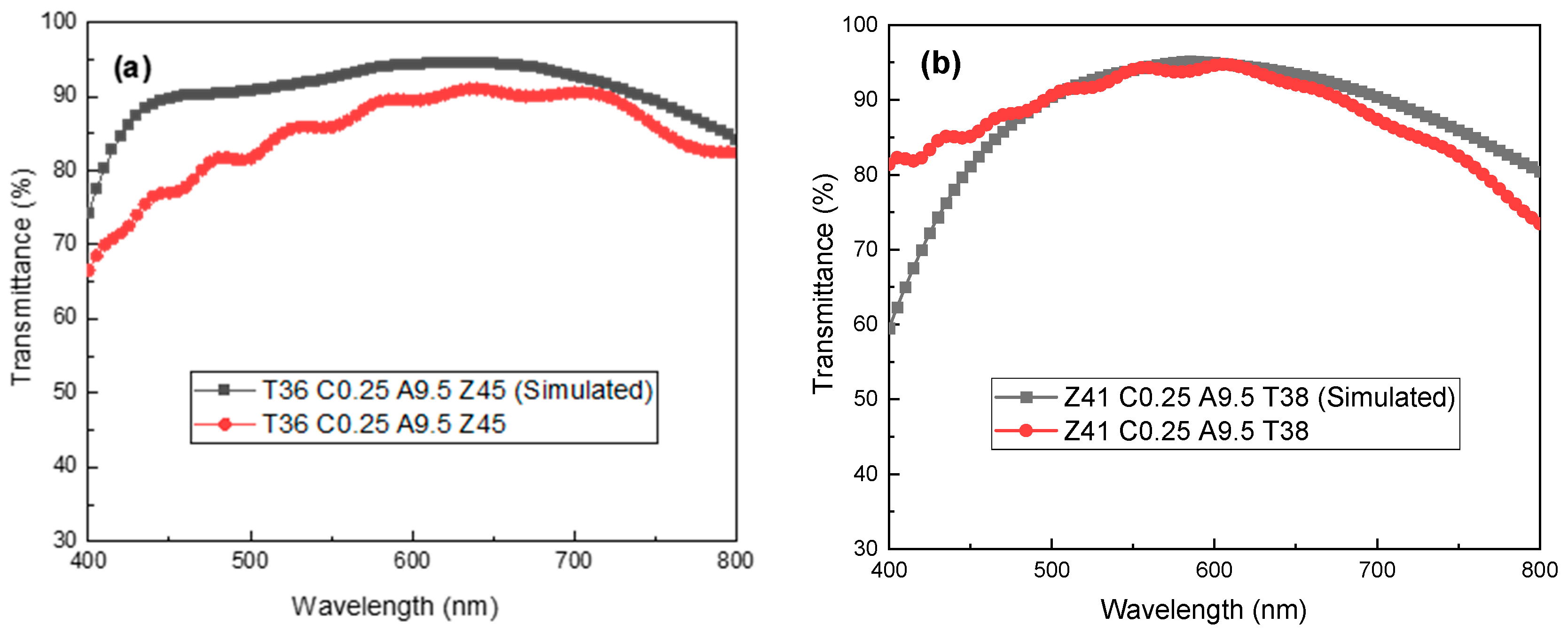
3.4. The Light Transmission of Asymmetric, Multilayered TCFs

The light transmission property was tested for the flexible samples with varied structures. The transmittance profiles in the spectrum of 350–1100 nm are displayed in Figure 4a for the samples with the TiO2/Cu/Ag/ZnS structure. The thickness of the sublayers for this sample group was 36 nm (TiO2), 0.25 nm (Cu) and 9.5 nm (Ag), with a variation in the range of 40–50 nm for the top ZnS layer. The transmittance curves follow the same trend of rising rapidly to a peak value (corresponding to the wavelength around 630 nm) and then falling off steadily from the near-ultraviolet zone to the near-infrared region. The three curves are close to each other in the ascending region. However, in the scope above a 630 nm wavelength, the transmittance values differ evidently with the increase of the ZnS layer thickness. The T36 C0.25 A9.5 Z45 sample appears to have the highest numbers, with T a v ( 400 800 ) of 84.75%, while the one with the 40 nm ZnS layer has the minimum values (detailed data are listed in Table 1). The wavy features of the transmittance profile should be attributed to the light interference effect among the sublayers and the PET substrate, which often appear in the multilayered TCFs [16,30].
The optical transmittance result for the other sample group with the ZnS/Cu/Ag/TiO2 structure is demonstrated in Figure 4b. The thickness numbers for sublayers are 41 nm (ZnS), 0.25 nm (Cu) and 9.5 nm (Ag) as constant parameters, while the top TiO2 layer varies from 31 to 45 nm in thickness. The transmittance profiles for this group generally present the similar parabolic patterns. Unlike the close distribution for TiO2/Cu/Ag/ZnS samples in the near-ultraviolet zone, the integral transmittance curves of the ZnS/Cu/Ag/TiO2 structure shift toward the near-infrared direction distinctly with an increase in the top layer thickness, with the maximum T a v ( 400 800 ) value of 88.46% for the Z41 C0.25 A9.5 T45 sample. The transmission properties of this group are obviously better in the visible light wavelength range of 400–800 nm, as listed in Table 1.

3.5. The Numerical Simulation of Light Transmission

One primary function of the dielectric layers in D/M/D-structured TCFs is acting as anti-reflection coatings to enhance the light transmission based on optical interference theory. Thickness optimization of the dielectric sublayers was conducted using TFCalc optical design software (version 3.8, by KLA Co., Milpitas, CA, USA), employing refractive index data for TiO2, ZnS, Ag, Cu and PET [31,32,33]. The simulation results from numerical modeling identified the optimal configurations of T36 C0.25 A9.5 Z45 and Z41 C0.25 A9.5 T38 for the two sets of multilayered structures in the visible spectrum. The comparison between the computational and experimental transmittance curves is demonstrated in Figure 5a,b.
For the TiO2/Cu/Ag/ZnS structure, the empirical data are significantly lower than the simulation data across the visible spectrum, with T a v ( 400 800 ) values of 84.75% and 90.6% respectively. Nevertheless, this configuration does present the best result in the group. On the other hand, the conformity between the two types of data is satisfying for the ZnS/Cu/Ag/TiO2 structure, with T a v ( 400 800 ) values of 87.9% for the experiment and 87.7% for the calculation, which confirms the validation of the simulation method applied.
The optical simulation assumes idealized multilayered structure conditions, including perfectly uniform and dense sublayers with smooth interfaces and surfaces. However, magnetron-sputtered TCFs usually deviate from these assumptions due to the existence of features like non-conformal interfacial bonding, localized microstructural heterogeneities and undulating interface profiles, which are factors unaccounted for in numerical models. Based on the morphology characteristics of the sublayers shown in Figure 1 and Figure 2, the excess light scattering loss and possible surface plasmon resonance from the inferior smoothness and compactness of the top ZnS layer [12,20,34], together with the imperfect continuity and smoothness of the metallic layer [14,18] in the TiO2/Cu/Ag/ZnS structure, should be the main reason for the poor transmittance results.

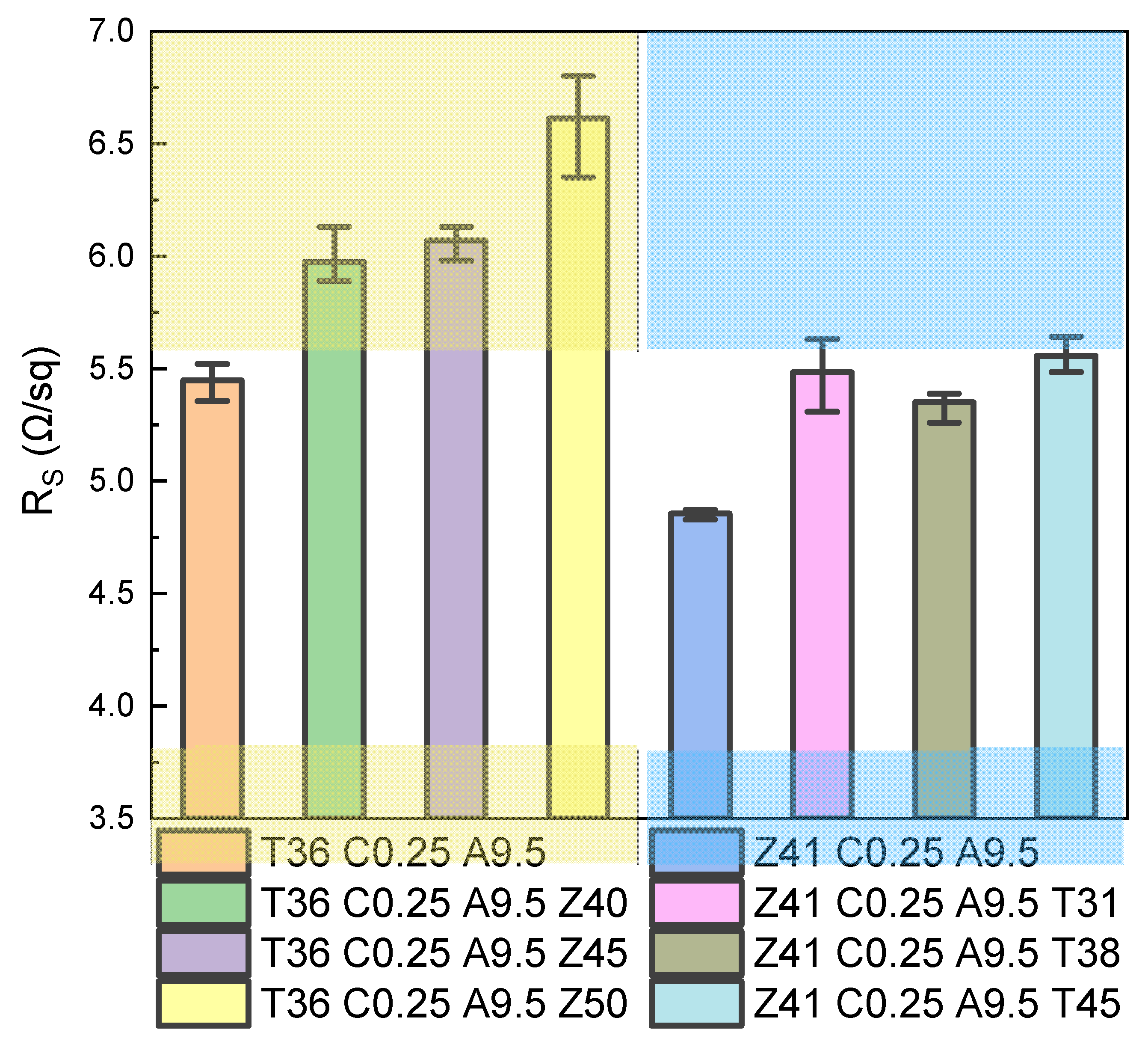
3.6. The Electrical Properties of Multilayered TCFs with Different Structures

The sheet resistance ( R S ) values of the two groups of multilayered samples are demonstrated in Figure 6, and detailed data are listed in Table 1. The samples with the TiO2/Cu/Ag/ZnS structure generally possess higher resistance, and the value grows with the increase in the thickness of the top layer, with a minimum number of 5.98 Ω/sq. In the other group with the ZnS/Cu/Ag/TiO2 structure, the value slightly fluctuates with the expansion of the top layer thickness, where the sample with the medium thickness of 38 nm for the top layer presents the minimum value of 5.35 Ω/sq.
The total R s of the multilayered TCF can be expressed as Equation (2):
1 R S = 1 R M + 1 R D 1 + 1 R D 2 ,
where R M , R D 1 and R D 2 denote the sheet resistances of the metallic and different dielectric layers, respectively. Given the significantly lower resistivity of metals compared to dielectrics, the equation could be simplified to R S R M . Thus, the total sheet resistance of the multilayer electrode is predominantly determined by the metallic layer. Nominally, all six TCF samples possess an identical bimetallic layer pattern; however, the final resistance values differ evidently. Therefore, the influence of two dielectric layers in the multilayers should be noted. The sheet resistance of multilayered samples with only bottom dielectric and metallic sublayers was tested. The results are 5.45 Ω/sq and 4.86 Ω/sq for the structures T36 C0.25 A9.5 and Z41 C0.25 A9.5, respectively. The better electrical performance of the ZnS bottom layer should be attributed its superior percolation properties [23,29] for continuous and homogeneous metallic layer forming, which is consistent with the satisfying morphology shown in Figure 2e. After the top dielectric layers were deposited to produce the complete D/M/D structure, although the ZnS/Cu/Ag/TiO2 structure maintained the better electrical conductivity, the sheet resistance increased to varied extents for the samples. The decline in the electrical property is believed to arise from the impingement effect or thermal effect from the deposition process of the top layer [35,36], which would jeopardize the continuity, uniformity or smoothness of the intermediate metallic layer.

3.7. The Figure of Merit for the Asymmetric, Multilayered TCFs

The optical and electrical properties of the multilayered samples are itemized in Table 1. Based on the transmittance and sheet resistance data, the figure of merit ( ϕ T C ) [37] was calculated according to Equation (3):
ϕ T C = T 10 / R S ,
where T denotes the light transmittance for a specific wavelength number or range (average).
The average FOM value in the visible light spectrum across 400–800 nm ( ϕ T C ( 400 800 ) ) is regarded as a critical indicator for the combination performance of transparent conductive materials. In the sample group of TiO2/Cu/Ag/ZnS structures, the ϕ T C ( 400 800 ) number varies with the increase in the top layer thickness from 40 nm to 50 nm, where the configuration of T36 C0.25 A9.5 Z45 exhibits the maximum result of 31.50 × 10⁻³ Ω−1. For the ZnS/Cu/Ag/TiO2-structured samples, the ϕ T C ( 400 800 ) values are obviously higher than in the first group. The Z41 C0.25 A9.5 T45 configuration achieves the peak value of 52.76 × 10⁻³ Ω−1. Furthermore, the FOM number remains high with the top layer thickness increasing from 38 nm to 45 nm, demonstrating the parameter-insensitive stability of performance, beneficial for the potential production application. The ϕ T C ( 550 ) value for each sample is also listed for reference, which is remarkably higher than ϕ T C ( 400 800 ) . However, the undulating feature of the transmittance curves here makes the former one less representative than the average value.

4. Discussion

The multilayered TCFs were prepared via a layer-wise magnetron sputtering process. The illustration of the interaction between sublayers on the morphology during the deposition process is shown in Figure 7. The bottom dielectric layer was the first one to be fabricated. In terms of materials, the TiO2 layer presents a smoother surface morphology than the ZnS (Figure 1), partly due to the denser microstructure provided by the higher RF power. Then, the intermediate metallic layer is deposited on the bottom layer. The seed layer should exist in a scattered, tiny island shape with a sub-nanometer thickness, which follows the Volmer-Weber model [38]. Afterward, the Ag layer, providing the prime electrical conductivity, was deposited. Although a lower surface roughness was offered by the TiO2 layer, the overall bimetal layer (with the seed layer) on ZnS layer reveals, evidently, the superior continuity and homogeneity in the morphology. The reason should be attributed to the better percolation property of ZnS for the metallic layer [11,29], especially the function of enhancing the promotion effect of the seed layer for the metallic film, forming at a minimum thickness (usually ≤10 nm). The top layer plays an important role not only in the anti-reflection of light but also in the protection of the TCF from deterioration in a corrosive environment [39] and to maintain its stability under high temperatures [15,40]. Compared with ZnS, the top TiO2 layer demonstrates satisfying characteristics of fine clusters and a smooth surface, which contributes well to the transparency of the asymmetric multilayer. Moreover, the ZnS/Cu/Ag/TiO2-structured samples maintained a stable performance for a few months in the natural environment due to the protection of the top layer with a dense structure, while the properties of the TiO2/Cu/Ag/ZnS samples deteriorated evidently within a few weeks.

5. Conclusions

The flexible TCFs with asymmetric TiO2/Cu/Ag/ZnS and ZnS/Cu/Ag/TiO2 structures were prepared via magnetron sputtering onto the flexible PET substrate, and their structural, optical and electrical properties were studied. The ZnS/Cu/Ag/TiO2 configuration demonstrates superior sublayer uniformity and optical and electrical performances to the TiO2/Cu/Ag/ZnS counterpart. The optical and electrical properties of the multilayers vary with the adjustment in the structure parameters. The optimal result of the ZnS/Cu/Ag/TiO2 film is 88.46% for the average transmittance in the visible spectrum and 5.56 Ω/sq for the sheet resistance, with the figure of merit achieving 52.76×10⁻³ Ω−1, while the best result of the TiO2/Cu/Ag/ZnS structure is 84.75%, 6.07 Ω/sq and 31.50×10⁻³ Ω−1, correspondingly. The bottom ZnS layer reveals its superior percolation property to facilitate bimetallic layer forming (including seed layer) with good continuity and homogeneity, although its original surface roughness is higher than TiO2. The top TiO2 layer demonstrates a satisfying morphology of fine clusters and a smooth surface with a dense structure, contributing greatly to the transmission properties of the multilayers. The rational utilization of interactions between sublayers during the sputtering-deposition is critical for the realization of optimal performance for the multilayered TCFs.

Author Contributions

Conceptualization, K.T. and Z.L.; methodology, K.T. and Q.L.; software, Q.L. and J.Z.; validation K.T. and J.Z.; formal analysis, J.Z. and Y.R.; investigation, Q.L. and J.Z.; resources, K.T. and Z.L.; data curation, Y.R. and J.Z.; writing—original draft preparation, Q.L.; writing—review and editing, K.T.; visualization, Q.L. and J.Z.; supervision, Z.L.; project administration, K.T.; funding acquisition, K.T. All authors have read and agreed to the published version of the manuscript.

Funding

This research was funded by the Science and Technology Project of Henan Province (No. 232102231016) and the Open Fund of Henan Key Laboratory of Advanced Cable Materials and Intelligent Manufacturing (No. CAMIM2025007).

Institutional Review Board Statement

Not applicable.

Informed Consent Statement

Not applicable.

Data Availability Statement

The raw data supporting the conclusions of this article will be made available by the authors on request.

Conflicts of Interest

The authors declare no conflicts of interest.

References

  1. Rabizadeh, M.; Ehsani, M.H. Effect of heat treatment on optical, electrical and thermal properties of ZnO/Cu/ZnO thin films for energy-saving application. Ceram. Int. 2022, 48, 16108–16113. [Google Scholar] [CrossRef]
  2. Wu, J.; Qian, X.; Liu, C.; Ji, Y.; Yu, S. Design and realization of neutral-tinted low-E film. Vacuum 2022, 203, 111228. [Google Scholar] [CrossRef]
  3. Lu, W.; Jiang, S.; Wa, P.; Yu, W.; Li, X.; Wu, L.; Ding, W.; Fu, G. Recent progress of multilayer composite transparent conductive film. Chin. Sci. Bull. 2017, 62, 372–384. [Google Scholar]
  4. Girtan, M.; Negulescu, B. A review on oxide/metal/oxide thin films on flexible substrates as electrodes for organic and perovskite solar cells. Opt. Mater. X 2022, 13, 100122. [Google Scholar] [CrossRef]
  5. Chen, X.; Zhang, N.; Wang, L.; Li, Y.; Yan, Y.; Li, X.; Xie, A.; Sun, D.; Han, J. Atomic Layer-deposited flexible ZnO transparent electrodes with Zn-Al-O interface for electrochromic devices. Ceram. Int. 2025, 51, 13018–13027. [Google Scholar] [CrossRef]
  6. Gerlein, L.F.; Benavides-Guerrero, J.A.; Cloutier, S.G. Photonic post-processing of a multi-material transparent conductive electrode architecture for optoelectronic device integration. RSC Adv. 2024, 14, 4748–4758. [Google Scholar] [CrossRef]
  7. Shugang, J.; Yue, W.; Haixu, L.; Wanbing, L.; Wei, Y. Research Progress of Flexible Organic/Inorganic Hybrid Perovskite Solar Cells. Chin. J. Lumin. 2018, 39, 1687–1696. [Google Scholar]
  8. Zhang, J.; Zhang, W.; Cheng, H.-M.; Silva, S.R.P. Critical review of recent progress of flexible perovskite solar cells. Mater. Today 2020, 39, 66–88. [Google Scholar] [CrossRef]
  9. Guillén, C.; Herrero, J. TCO/metal/TCO structures for energy and flexible electronics. Thin Solid Film. 2011, 520, 1–17. [Google Scholar] [CrossRef]
  10. Lee, S.-M.; Koo, H.-W.; Kim, T.-W.; Kim, H.-K. Asymmetric ITO/Ag/ZTO and ZTO/Ag/ITO anodes prepared by roll-to-roll sputtering for flexible organic light-emitting diodes. Surf. Coat. Technol. 2018, 343, 115–120. [Google Scholar] [CrossRef]
  11. Han, Y.C.; Lim, M.S.; Park, J.H.; Choi, K.C. ITO-free flexible organic light-emitting diode using ZnS/Ag/MoO3 anode incorporating a quasi-perfect Ag thin film. Org. Electron. 2013, 14, 3437–3443. [Google Scholar] [CrossRef]
  12. Jin, J.; Liu, C.; Yang, Z.-j.; Wang, L. The influence of AZO films on morphology and surface plasmon resonance properties of Ag particles. Surf. Coat. Technol. 2019, 363, 135–141. [Google Scholar] [CrossRef]
  13. Lee, K.-C.; Lin, S.-J.; Lin, C.-H.; Tsai, C.-S.; Lu, Y.-J. Size effect of Ag nanoparticles on surface plasmon resonance. Surf. Coat. Technol. 2008, 202, 5339–5342. [Google Scholar] [CrossRef]
  14. Maniyara, R.A.; Rodrigo, D.; Yu, R.; Canet-Ferrer, J.; Ghosh, D.S.; Yongsunthon, R.; Baker, D.E.; Rezikyan, A.; García de Abajo, F.J.; Pruneri, V. Tunable plasmons in ultrathin metal films. Nat. Photonics 2019, 13, 328–333. [Google Scholar] [CrossRef]
  15. Li, B.-J.; Yang, G.-Y.; Huang, L.-J.; Wang, T.-Y.; Ren, N.-F. Effects of BN layer on photoelectric properties and stability of flexible Al/Cu/ZnO multilayer thin film. Ceram. Int. 2020, 46, 14686–14696. [Google Scholar] [CrossRef]
  16. Dhar, A.; Alford, T.L. High quality transparent TiO2/Ag/TiO2 composite electrode films deposited on flexible substrate at room temperature by sputtering. APL Mater. 2013, 1, 12102. [Google Scholar] [CrossRef]
  17. Formica, N.; Mantillaperez, P.; Ghosh, D.S.; Janner, D.; Tong, L.C.; Huang, M.; Garner, S.; Martorell, J.; Pruneri, V. An ITO-free polymer solar cell on flexible glass. ACS Appl. Mater. Interfaces 2015, 7, 4541. [Google Scholar] [CrossRef]
  18. Jiang, S.; Feng, L.; Zhang, W.; Liu, H.; Liu, H.; Liu, Y.; Li, B.; Wu, L.; Liu, X.; Wang, X.; et al. Indium-free flexible perovskite solar cells with AZO/Cu/Ag/AZO multilayer transparent electrodes. Sol. Energy Mater. Sol. Cells 2022, 246, 111895. [Google Scholar] [CrossRef]
  19. Lim, S.; Han, D.; Kim, H.; Lee, S.; Yoo, S. Cu-based multilayer transparent electrodes: A low-cost alternative to ITO electrodes in organic solar cells. Sol. Energy Mater. Sol. Cells 2012, 101, 170–175. [Google Scholar] [CrossRef]
  20. Mouchaal, Y.; Louarn, G.; Khelil, A.; Morsli, M.; Stephant, N.; Bou, A.; Abachi, T.; Cattin, L.; Makha, M.; Torchio, P.; et al. Broadening of the transmission range of dielectric/metal multilayer structures by using different metals. Vacuum 2015, 111, 32–41. [Google Scholar] [CrossRef]
  21. Guan, M.; Wang, L.; Zhang, Y.; Wang, D.; Wang, Q.; Liu, J. Effect of metal seed layer on the critical thickness and photoelectric properties of ultrathin Ag films. Mater. Today Commun. 2023, 37, 107540. [Google Scholar] [CrossRef]
  22. Meiss, J.; Riede, M.K.; Leo, K. Towards efficient tin-doped indium oxide (ITO)-free inverted organic solar cells using metal cathodes. Appl. Phys. Lett. 2009, 94, 013303. [Google Scholar] [CrossRef]
  23. Formica, N.; Ghosh, D.S.; Carrilero, A.; Chen, T.L.; Simpson, R.E.; Pruneri, V. Ultrastable and atomically smooth ultrathin silver films grown on a copper seed layer. ACS Appl. Mater. Interfaces 2013, 5, 3048–3053. [Google Scholar] [CrossRef]
  24. Liao, J.; Qian, R.; Wang, G.; Chen, N.; Xu, S.; Hu, S.; Zhu, W.; Luo, G. High performances multilayer transparent conductive films with manipulated Ag growth and layer thickness. J. Mater. Sci. Mater. Electron. 2023, 34, 795. [Google Scholar] [CrossRef]
  25. Kao, P.-C.; Hsu, C.-J.; Chen, Z.-H.; Chen, S.-H. Highly transparent and conductive MoO3/Ag/MoO3 multilayer films via air annealing of the MoO3 layer for ITO-free organic solar cells. J. Alloys Compd. 2022, 906, 164387. [Google Scholar] [CrossRef]
  26. Cho, H.; Yun, C.; Park, J.-W.; Yoo, S. Highly flexible organic light-emitting diodes based on ZnS/Ag/WO3 multilayer transparent electrodes. Org. Electron. 2009, 10, 1163–1169. [Google Scholar] [CrossRef]
  27. Kermani, H.; Fallah, H.R.; Hajimahmoodzadeh, M. Design and fabrication of nanometric ZnS/Ag/MoO3 transparent conductive electrode and investigating the effect of annealing process on its characteristics. Phys. E Low-Dimens. Syst. Nanostruct. 2013, 47, 303–308. [Google Scholar] [CrossRef]
  28. Peng, C.H.; Chen, P.S.; Lo, J.W.; Lin, T.W.; Lee, S.W. Indium-free transparent TiOx/Ag/WO3 stacked composite electrode with improved moisture resistance. J. Mater. Sci. Mater. Electron. 2016, 27, 12060–12066. [Google Scholar] [CrossRef]
  29. Kim, D.-Y.; Han, Y.C.; Kim, H.C.; Jeong, E.G.; Choi, K.C. Highly Transparent and Flexible Organic Light-Emitting Diodes with Structure Optimized for Anode/Cathode Multilayer Electrodes. Adv. Funct. Mater. 2015, 25, 7145–7153. [Google Scholar] [CrossRef]
  30. Li, B.-J.; Li, Z.-X.; Huang, L.-J.; Wang, L.; Ren, N.-F. Preparation of AZO-based multilayer thin films with high comprehensive properties by introducing Cu/Ag bimetallic layers. J. Mater. Sci. Mater. Electron. 2023, 34, 832. [Google Scholar] [CrossRef]
  31. Johnson, P.B.; Christy, R.W. Optical Constants of the Noble Metals. Phys. Rev. B 1972, 6, 4370–4379. [Google Scholar] [CrossRef]
  32. Zhang, X.; Qiu, J.; Zhao, J.; Li, X.; Liu, L. Complex refractive indices measurements of polymers in infrared bands. J. Quant. Spectrosc. Radiat. Transf. 2020, 252, 107063. [Google Scholar] [CrossRef]
  33. Kamptner, A.; Scharber, M.C.; Schiek, M. Accurate Determination of the Uniaxial Complex Refractive Index and the Optical Band Gap of Polymer Thin Films to Correlate their Absorption Strength and Onset of Absorption. ChemPhysChem 2024, 25, e202400233. [Google Scholar] [CrossRef] [PubMed]
  34. Chen, Z.; Huang, J.; Chen, Z.; Hu, Y.; Li, H.; Zhang, R.; Tang, K.; Wang, L. Influence of Cu Thickness and Annealing on the Properties of ZnS/Cu/ZnS Multilayer Films. J. Electron. Mater. 2020, 49, 4498–4503. [Google Scholar] [CrossRef]
  35. Ren, N.-F.; Wang, W.-Z.; Li, B.-J.; Huang, L.-J.; Zhang, Y. Preparation and property optimization of silver-embedded FTO transparent conductive thin films by laser etching and coating AZO layer. J. Mater. Sci. Mater. Electron. 2021, 32, 10644–10661. [Google Scholar] [CrossRef]
  36. Zhu, H.; Zhang, Y.; Zhao, L.; Nie, L.; Liu, J. Preparation of Ag-based transparent conductive films with high figure-of-merit from dielectric layers’ combination. Opt. Quantum Electron. 2024, 57, 40. [Google Scholar] [CrossRef]
  37. Haacke, G. New figure of merit for transparent conductors. J. Appl. Phys. 1976, 47, 4086–4089. [Google Scholar] [CrossRef]
  38. Yun, J. Ultrathin Metal films for Transparent Electrodes of Flexible Optoelectronic Devices. Adv. Funct. Mater. 2017, 27, 1606641. [Google Scholar] [CrossRef]
  39. Wan Shamsuddin, W.N.S.; Zuber, K.; Murphy, P.J.; Jane, M.L. Environmental durability of soft low-e coatings: A review. Sol. Energy Mater. Sol. Cells 2024, 266, 112673. [Google Scholar] [CrossRef]
  40. Yu, S.; Song, L.; Wu, C.; Li, L. Enhanced conductivity and stability of Cu-embedded zinc tin oxide flexible transparent conductive thin films. Ceram. Int. 2022, 48, 15925–15931. [Google Scholar] [CrossRef]
Figure 1. The AFM images of surfaces for the PET substrate and the dielectric layers: (a) PET; (b) PET/TiO2; (c) PET/ZnS.
Coatings 15 00650 g001
Figure 2. The SEM images of surface morphology for the flexible, multilayered film: (a) TiO2/Ag; (b) TiO2/Cu/Ag; (c) TiO2/Cu/Ag/ZnS; (d) ZnS/Ag; (e) ZnS/Cu/Ag; (f) ZnS/Cu/Ag/TiO2.
Coatings 15 00650 g002
Figure 3. The diffraction pattern of TiO2/Cu/Ag/ZnS multilayer via GIXRD.
Coatings 15 00650 g003
Figure 4. The transmittance curves of flexible, multilayered TCFs with different structures: (a) TiO2/Cu/Ag/ZnS; (b) ZnS/Cu/Ag/TiO2.
Coatings 15 00650 g004
Figure 5. The light transmittance comparison between the simulation and experiment for the multilayered TCFs: (a) T36 C0.25 A9.5 Z45; (b) Z41 C0.25 A9.5 T38.
Coatings 15 00650 g005
Figure 6. The sheet resistance of multilayered TCFs with different structures.
Coatings 15 00650 g006
Figure 7. An illustration of the interaction between sublayers on the morphology during the deposition of multilayered TCFs.
Coatings 15 00650 g007
Table 1. The optical and electrical properties of flexible, multilayered TCFs.
TCF R S
(Ω/sq)
T 550
(%)
T a v ( 400 800 )
(%)
ϕ T C ( 550 )
(10−3 Ω−1)
ϕ T C ( 400 800 )
(10−3 Ω−1)
T36 C0.25 A9.5 Z405.9887.2082.9942.5225.93
T36 C0.25 A9.5 Z456.0785.8384.7535.7431.50
T36 C0.25 A9.5 Z506.6485.9883.9133.2626.07
Z41 C0.25 A9.5 T315.4895.2186.65111.6643.52
Z41 C0.25 A9.5 T385.3594.0487.90101.1551.47
Z41 C0.25 A9.5 T455.5692.7088.4684.3452.76
Disclaimer/Publisher’s Note: The statements, opinions and data contained in all publications are solely those of the individual author(s) and contributor(s) and not of MDPI and/or the editor(s). MDPI and/or the editor(s) disclaim responsibility for any injury to people or property resulting from any ideas, methods, instructions or products referred to in the content.

