1. Introduction
Piezoelectric thin-film-based resonators, sensors, and actuators [
1,
2,
3,
4] are garnering increasing attention in various acoustoelectric conversion and microwave telecommunications applications. The performances of those piezoelectric devices mainly depend on the choice of piezoelectric materials. AlN thin films possess high thermal stability, high acoustic velocity, low acoustic loss, and, in particular, good Si-microfabrication compatibility, which is promising for integrated sensors/actuators on silicon substrates. Compared with traditional piezoelectric thin film such as PbZr
1−xTi
xO
3 (PZT) thin films, intrinsic AlN thin films show a small longitudinal piezoelectric coefficient (
d33 = 6.3pC/N) [
5] and a corresponding limited electromechanical coupling coefficient, 6–7% [
6]. To address performance limitations in ultra-high-sensitivity transducers and microwave filters’ application scope [
7,
8], Al
1−xSc
xN piezoelectric thin films were developed in the past decade. It is agreed that the piezoelectric response of Al
1−xSc
xN thin films increases upon Sc content. The Akiyama team [
9] pioneered a leap in piezoelectric performance (
d33 = 27.6 pC/N) in Al
0.57Sc
0.43N thin-film systems. Hirata et al. [
10] utilized a lutetium (Lu) interlayer technique with an hexagonal close-packed (HCP) crystal structure, elevating the Sc doping threshold from
x = 0.430 to
x = 0.508. This advancement achieved dual optimization of heteroepitaxial quality and (0002) crystallographic preferential orientation, culminating in a record-breaking
d33 value of 35.5 pC/N. Liffredo et al. [
11] obtained a 5× improvement in piezoelectric coupling compared to undoped AlN and a 1.5× improvement from 32% doped Al
1−xSc
xN in Al0.6Sc0.4N thin film. Tasnádi et al. [
12] employed first-principles calculations to confirm that this performance enhancement originated from Sc doping-induced chemical bond reorganization—specifically, a synergistic mechanism combining lattice softening (50% reduction in elastic stiffness
C33) and potential energy flattening.
However, the immiscible structure of ScN (rock salt, cubic) and AlN (wurtzite, hexagonal) and large differences in cation radii make it difficult to fabricate high-quality wurtzite structure thin films. It is agreed that the wurtzite phase of AlN and Al
1−xSc
xN thin film presents superior lattice matching with a hexagonal crystal system, such as sapphire. Höglund et al. [
13] investigated the Al
1−xSc
xN thin films deposited on Al
2O
3(0001) and reported that the wurtzite structure persisted when the Sc atomic fraction
x ≤ 22%, dual-phase coexistence occurred in the range 22% <
x ≤ 50%, and a cubic phase formed when
x > 50% for the Al
1−xSc
xN system. Zhu et al. [
14] reported that Al
1−xSc
xN with an AlN intermediate layer exhibited a wider optical bandgap. This was mainly attributed to the growth of the AlN layer on c-sapphire prior to the deposition of Al
1−xSc
xN, which helped improve lattice matching and reduce the defect density in the bandgap. On the other hand, the performance of thin films highly demands high-quality film. The mainstream preparation methods are Al and Sc individual target co-sputtering deposition [
15,
16,
17,
18] and alloy target sputtering [
10,
19]. Co-sputtering can produce films with various Sc contents, which is beneficial for research. Alloy targets’ sputtering technique is more advantageous for practical production due to its faster deposition rates and a more uniform chemical composition of the film.
In this work, Al1−xScxN thin films were fabricated by radio frequency–magnetron sputtering technology with alloy targets. The crystal structure, orientation, and electric properties of the as-prepared Al1−xScxN thin films were investigated.
2. Materials and Methods
Al
1−xSc
xN thin films were deposited on Mo/p-Si (100) substrates using a radio frequency–magnetron sputtering system. The aluminum sputtering target had a diameter of 70 mm and a purity of 99.999%. Al
1−xSc
x alloy targets with different compositions (
x = 0, 0.25, 0.3, 0.4, and 0.55) were utilized to fabricate thin films. The molybdenum layer was sputtered using a Mo metal target with a diameter of 70 mm and a purity of 99.999%. Al
1−xSc
x alloy targets with various Sc contents exhibited distinct requirements for background gas concentrations and power during sputtering. The nitrogen-to-argon ratio and sputtering power were adjusted to facilitate the growth of thin films oriented along the (0002) direction. Additionally, as the structural distortion within the lattice system significantly increased the complexities of thin film growth with the increasing Sc content, the Mo layer sputtering time of Al
1−xSc
xN (
x = 0, 0.2, 0.25, 0.3, and 0.43) thin films was also adjusted to facilitate the growth of thin films oriented along (0002). The sputtering time for the Mo layer of AlN (
x = 0) thin films and Al
1−xSc
xN (
x = 0.2, 0.25, 0.3 and 0.43) thin films was 5 min and 15 min, respectively. The sputtering time for Al
1−xSc
xN (
x = 0, 0.2, 0.25, 0.3, and 0.43) thin films was 50 min. The sputtering conditions for the fabrication are summarized in
Table 1.
The phase structure of the thin film sample was characterized by X-ray diffraction (DX-2700, Dandong, China) with Cu Kα radiation (λ = 0.15406 nm). The GIWAXS/XRR data were obtained at the 1W1A Diffuse X-ray Scattering Station, Beijing Synchrotron Radiation Facility (BSRF-1W1A), China. The cross-sectional morphology of the film was observed by a field emission scanning electron microscope (Thermo Scientific, Helios G4 UC, Waltham, MA, USA). The compositions of the target material and thin films were characterized and confirmed using an energy-dispersive spectrometer (EDS) with a field emission scanning electron microscope (Thermo Scientific, Helios G4 UC, Waltham, MA, USA). The dielectric properties, such as the relationship between the dielectric constant and the frequency, were tested using the LCR Meter (TH2829C, Guangzhou, China). The leakage current tests of the thin films were measured by the Radiant Precision Workstation (RT6000, Albuquerque, NM, USA) combined with the HFS600E-PB4 probe station manufactured by UK-based Linkam Scientific Instruments (Newbury, Berkshire, UK).
3. Results
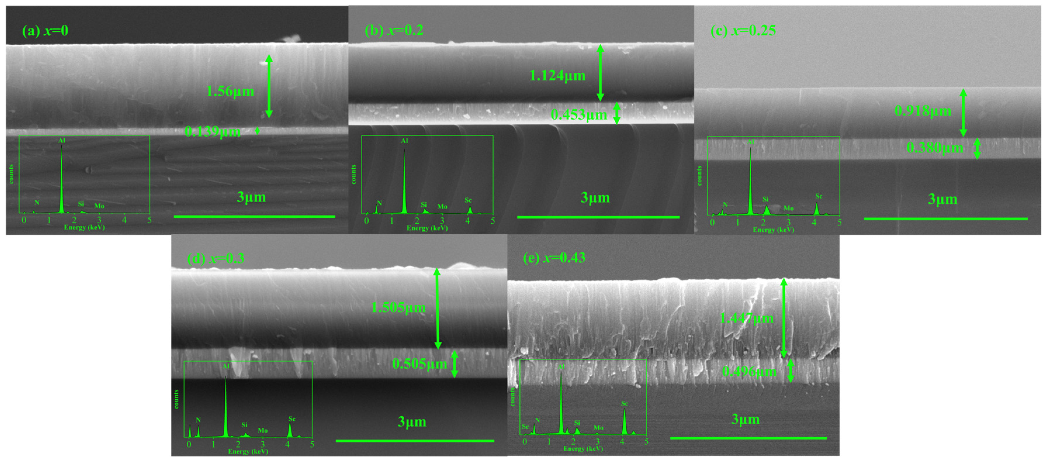
Figure 1 presents cross-sectional SEM morphology images of Al
1−xSc
xN thin films with different Sc contents. From the cross-sectional images, it is evident that the films maintained a dense structure and grew via a columnar crystal mode regardless of the Sc concentration. Even though all Al
1−xSc
xN (
x = 0, 0.2, 0.25, 0.3, and 0.43) thin films were deposited for the same duration, they showed various thicknesses. The different deposition rate resulted from the combined effects of Al
1−xSc
x alloy targets’ chemical composition and distinct sputtering processing parameters (see
Table 1). The AlN thin film demonstrated more controlled growth characteristics during the deposition processes, with around 120 nm Mo layers as the buffer. However, the lattice distortion of the Al
1−xSc
xN thin films intensified significantly with the increasing Sc content. As a result, thicker Mo buffer layers were needed to induce the oriented growth of the prepared thin films, as shown in
Figure 1. The energy-dispersive spectrometer (EDS) results of the thin films show that the chemical composition of all the thin films tested was Al
1−xSc
xN with
x = 0, 0.2, 0.25, 0.3, and 0.43, respectively.
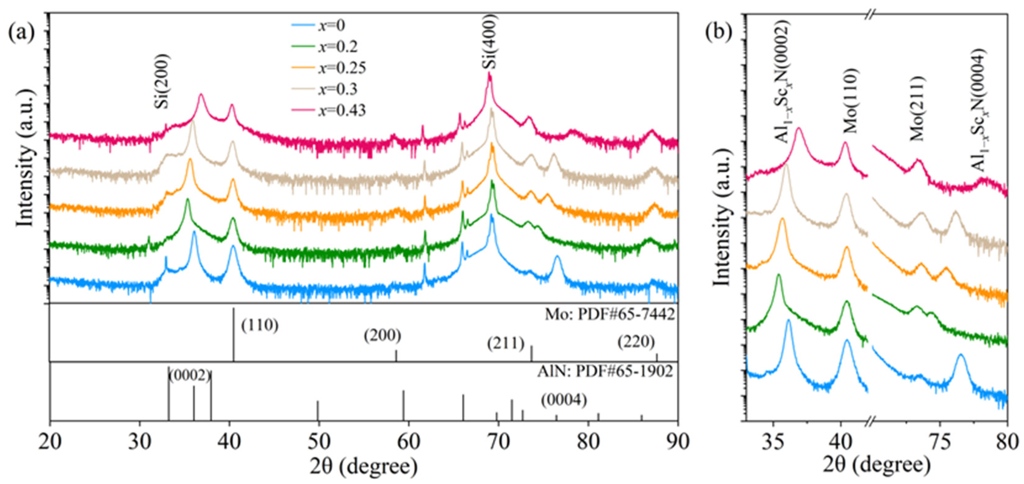
Figure 2 shows the XRD results of the as-prepared Al
1−xSc
xN films. The only observed diffraction peaks correspond to wurtzite AlN (0002), (0004) and Al
1−xSc
xN (0002), (0004) cubic Mo (110), (200), (211) seed layer, and cubic Si (200), (400) substrate compared with those of PDF card # 65-1902 AlN, card # 65-7442 Mo, and card # 80-0018 Si, respectively. The results indicate that all Al
1−xSc
xN films crystallized in the wurtzite structure and exhibited preferential growth along the (0002) orientation. The shifts in the (0002) and (0004) diffraction peaks revealed the modulation of the Sc concentration to the out-of-plane lattice constant. The
c-axis length of the Al
1−xSc
xN thin films increased with the increase in the x values, ranging from 0.2 to 0.3. The obvious right shift in the (0002) and (0004) diffraction peaks indicated a decrease in
c-axis length for the Al
0.57Sc
0.43N thin film.
The
c-axis values and full width at half maximum (FWHM) of the (0002) diffraction peaks from the data in
Figure 2a of all Al
1−xSc
xN thin films are given in
Table 2. The FWHM showed an increasing trend, which was attributed to the intensified lattice distortion with the increase in Sc content in the prepared Al
1−xSc
xN thin films.
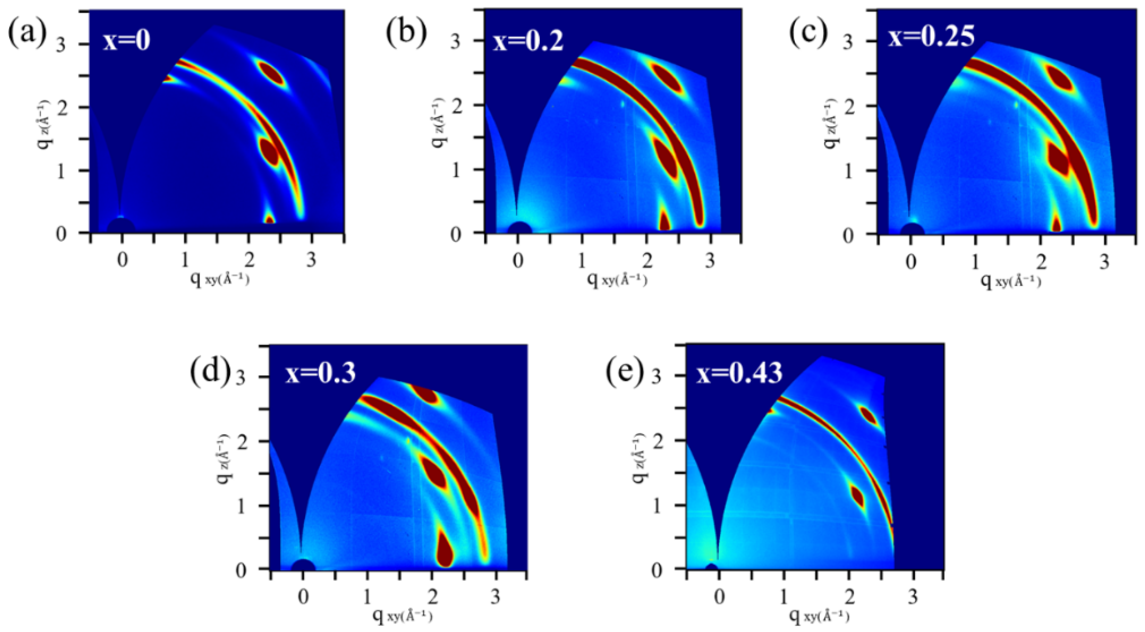
The determination of lattice parameters in crystalline materials is critical for material analysis. Grazing-incidence wide-angle X-ray scattering (GIWAXS) was employed to further investigate the influence of scandium incorporation on the crystal structure of Al
1−xSc
xN. Compared to conventional laboratory-based XRD, synchrotron radiation X-ray scattering exhibits higher brightness [
20]. This approach enables the capture of all scattered signals, which is particularly advantageous for highly textured thin-film samples, as most diffraction peaks are often missed in laboratory XRD data. The hexagonal wurtzite crystal model of AlN and the rock salt-phase crystal model of ScN were constructed using the VESTA tool(ver. 3. 5. 8). The GIWAXS-tools (ver. 2. 3. 14) software was subsequently employed to simulate the GIWAXS patterns based on these models. The constructed crystal models and their corresponding simulated GIWAXS results are displayed in
Figure 3. From the simulated results, it can be observed that, when Sc completely replaces Al atoms and forms a fully cubic rock salt phase, the (10
0), (10
1), and (10
2) diffraction spots disappear from the first quadrant, while the (111), (101), and (112) diffraction spots emerge.
Figure 4a–e display the GIWAXS test results of the as-prepared Al
1−xSc
xN thin films. Consistent with the simulated patterns in
Figure 3a, three distinct diffraction spots corresponding to the (10
0), (10
1), and (10
2) crystallographic planes can be observed in
Figure 4a–d for the prepared Al
1−xSc
xN thin films with
x = 0, 0.2, 0.25, and 0.3. For the thin film with
x = 0.43, the (10
0) diffraction spot is absent, which reveals significant lattice distortion due to the large amount of Al atoms being replaced by Sc atoms at this Sc concentration. All the discrete spots indicate the high crystallinity of the prepared thin films. After Sc atom doping, the diffraction spots of (10
0), (10
1), and (10
2) exhibit slight broadening, indicating that Sc doping induces a certain degree of reduction in the overall crystallinity. The ring-shaped diffraction streaks originate from the (110) plane of the cubic polycrystalline Mo layer, reflecting its polycrystalline growth characteristics.
The scattering peaks observed in the
q-space are objectively convertible to the 2
θ-angle coordinate system, governed by Bragg’s law:
The interplanar spacing
d can be determined as follows:
The interplanar spacing
d of the hexagonal system is given by the following:
where
h,
k, and
l are indices of the crystal plane, and d is the interplanar spacing. By combining Equations (2) and (3), the lattice parameters
a and
c values of the as-prepared Al
1−xSc
xN thin films could be calculated from the GIWAXS data, as shown in
Figure 5.
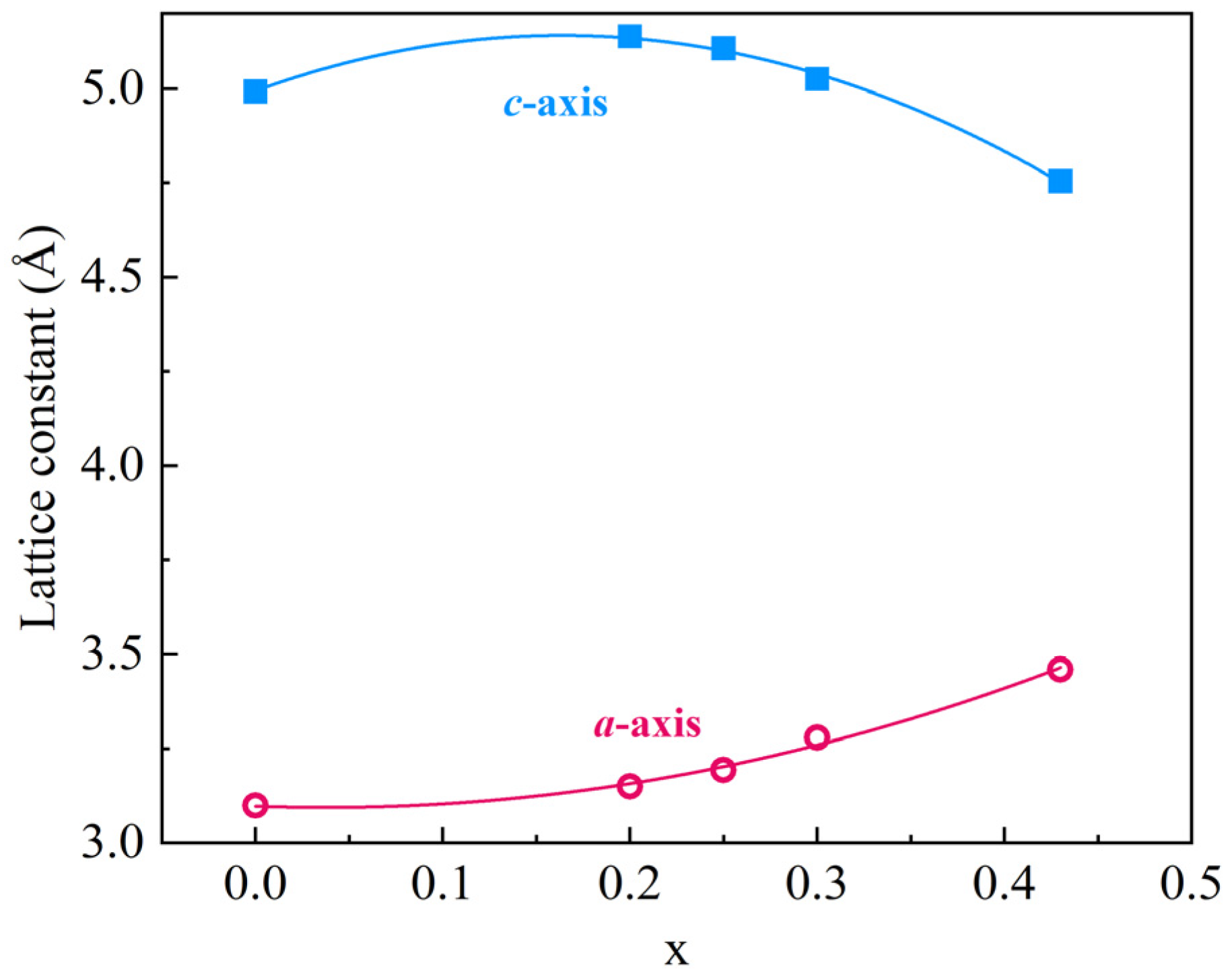
The curves in
Figure 5 indicate that both the
a-axis and
c-axis lattice parameters exhibit nonlinear variations with increasing Sc concentration. The
a-axis parameter demonstrates a monotonic increase from 3.0998 Å at (
x = 0) to 3.4602 Å (
x = 0.43), corresponding to a relative expansion of 11.6%. In contrast, the
c-axis parameter displays two-stage mild evolution: it initially rises from 4.9925 Å (
x = 0) to 5.1387 Å (
x = 0.2) with 2.9% expansion and is then followed by a progressive contraction to 4.7544 at
x = 0.43. This different behavior suggests distinct structural responses of the lattice distortion to Sc concentration.
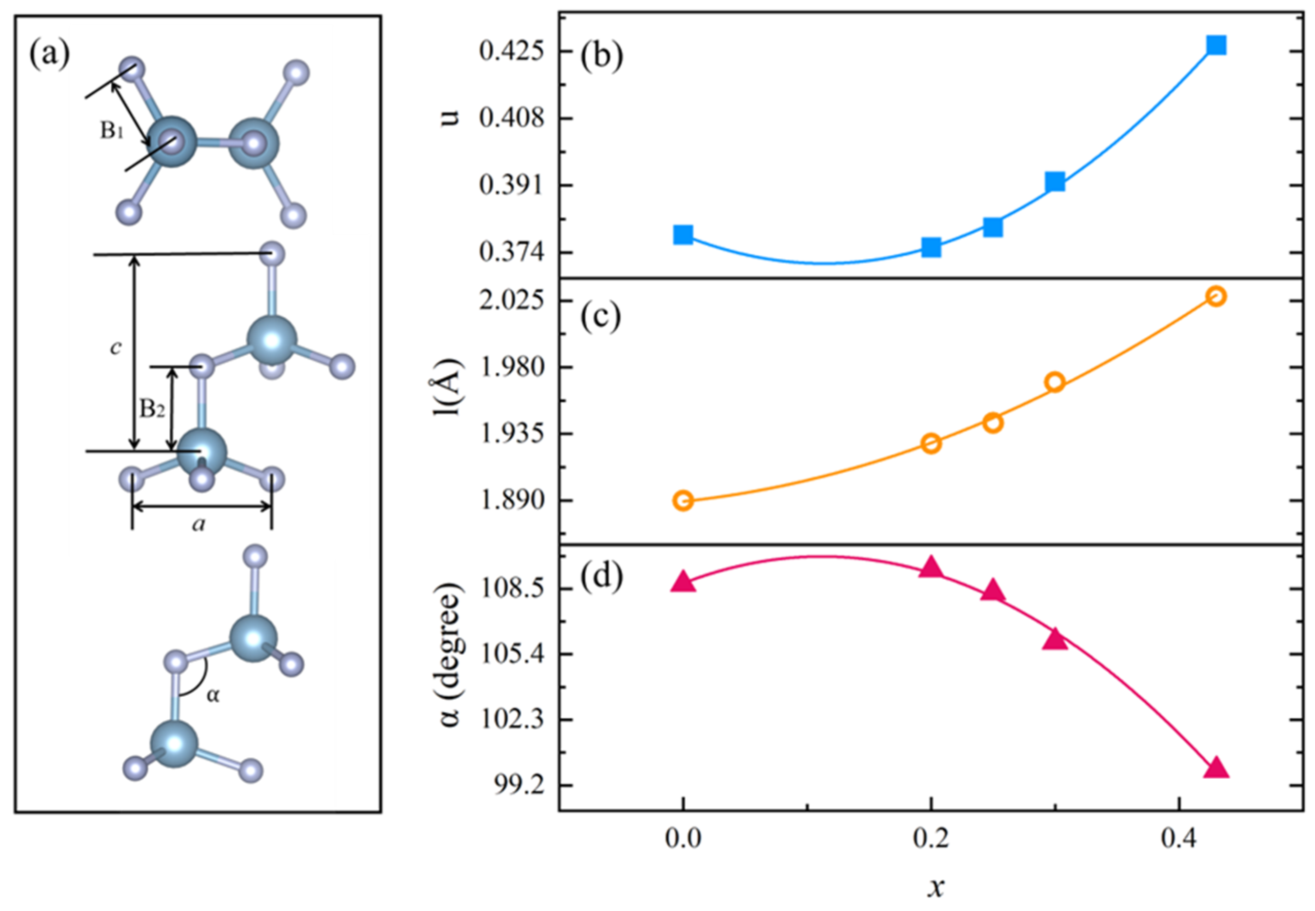
Figure 6a illustrates the 3D schematic diagrams of the unit cell parameters (
a,
c) and bond lengths (
ℓ1,
ℓ2) as well as bond angle (
α) in the AlN molecular structure. In AlN, the B1 bond length is designated as
ℓ1, the B
2 bond length as
ℓ2, and the Al–N–Al bond angle between B
1 and B
2 bonds as
α. A critical parameter in the wurtzite structure, denoted as
u =
ℓ2/c, quantifies the fractional deviation of specific atomic positions from their ideal lattice sites. Specifically,
u represents the ratio of the B
2 bond length along the
c-axis to the total
c-axis length.
The lengths of the
c-axis-parallel B2 bond (ℓ
2) and the in-plane B1 bond (ℓ
1) are ex-pressed as follows [
15]:
Assuming ℓ
1 = ℓ
2 = ℓ (for AlN, this approximation induces an error <1% [
21]), the coupled solutions of Equations (4) and (5) yield the following:
Given the internal parameters, the bond length
ℓ can be calculated using Equation (4), and the bond angle
α is determined through Equation (7):
The calculated results of the internal parameter
u, bond length
ℓ, and bond angle
α are shown in
Figure 6b–d. The monotonic expansion of the
a-axis lattice parameter is primarily dominated by
ℓ, as evidenced by the proportional correlation between their monotonic increases across the entire doping range. In contrast, the non-monotonic variation in the c-axis arises from the synergistic interplay between bond length and bond angle. At lower Sc concentrations (
x < 0.2), the minimal angular distortion allows bond elongation to govern c-axis expansion. However, when
x > 0.2, the rapidly decreasing bond angle progressively overtakes the bond lengthening effect through enhanced interlayer compression, ultimately driving the
c-axis contraction. This competition between bond geometry parameters quantitatively explains the characteristic “increase-then-decrease” behavior observed in
c-axis evolution.
Figure 7a shows that the dielectric property characterization of Al
1−xSc
xN thin films reveals a remarkable upward trend in relative permittivity with increasing Sc composition. Experimental data demonstrate that the relative permittivity increases from 10.66 to 34.67 as the Sc content rises from 0 to 0.43, corresponding to a polynomial-fitting-derived relative growth rate of 225%. This enhancement mechanism arises from lattice distortion and enhanced local dipole moments induced by the incorporation of Sc ions.
The relative permittivity results were compared with the published literature. Data from Kurz 2019 [
22] and Yanagitani 2014 [
23] exhibit similar trends with minor absolute value deviations, yet consistently reinforce the conclusion that elevated Sc concentrations amplify permittivity.
Figure 7b demonstrates the variation in dielectric loss (tanδ) for Al
1−xSc
xN thin films at 1 MHz as a function of scandium concentration (
x = 0, 0.2, 0.25, 0.3, and 0.43). The undoped sample (
x = 0) exhibited an average dielectric loss value of 0.15%. As the Sc concentration increased to
x = 0.43, the dielectric loss rose significantly to 6.7%. The enhanced dissipation could be attributed to the following mechanisms: the substitution of Al
3+ by Sc
3+ formed Sc-N bonds with stronger ionic characteristics compared to the original Al-N bonds (Born effective charge increased from 2.82 to 3.16). Although this bonding modification effectively enhanced the piezoelectric coefficients, it simultaneously induced relaxation hysteresis in the ionic displacement response of the lattice under external electric fields. Specifically, under MHz-level high-frequency alternating fields, the delayed recombination process between defect centers and polar domain walls acted as an additional energy dissipation channel.
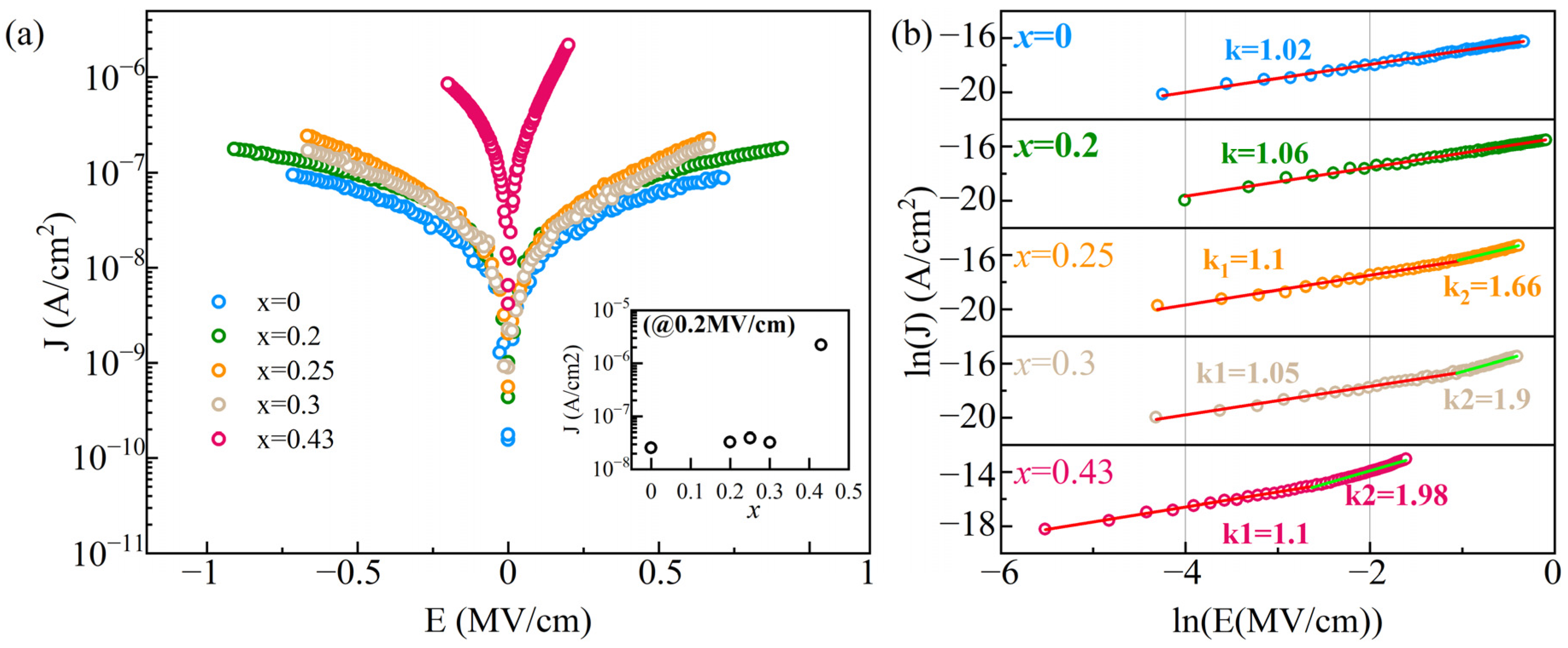
Figure 8 illustrates the dependence of electric field transport properties in Al
1−xSc
xN thin films on Sc doping concentration. By sweeping the applied electric field from −1 to +1 MV/cm, leakage current evolution curves were obtained for samples with varying Sc compositions (
x = 0, 0.2, 0.25, 0.3, and 0.43). The leakage current not only reflected material insulation performance but also correlated with defect density, interfacial quality, and electrical stability. The
J-E characteristics could be described by the following relationship:
In the equation, e, n, μ, and E denote the electronic charge, free charge carrier density, carrier mobility in the dielectric, and the applied electric field strength across the dielectric material, respectively.
The experimental results demonstrate a slight upshift in overall current density profiles with incremental increases in Sc doping level
x (
x ≦ 0.3), exhibiting a particularly abrupt increase at
x = 0.43 (the inset provides the leakage current density values of the Al
1−xSc
xN thin films at 0.2 MV/cm). This phenomenon reflects that Sc incorporation significantly modulated the microscopic charge transport mechanisms within the material. There are seldom reports on the leakage density of Al
1−xSc
xN thin films. Rudresh et al. [
24] reported that the leakage density of the Al
1−xSc
xN thin film decreased compared with the AlN thin film in their research, but unfortunately did not refer to any Sc content in the thin films. The electronic properties of Al
1−xSc
xN as a function of Sc distribution were studied using density functional theory (DFT). Bhattarai et al. [
25] and Yang et al. [
26] reported that the gap in Al
1−xSc
xN thin films decreased continuously with increasing Sc concentration, and the prominently small bandgap of Al
1−xSc
xN thin films corresponded to high electric conductivity.
The logarithmic scaling of current–voltage characteristics in
Figure 8b (ln(
J)–ln(
E) correlation) reveals critical transitions in charge transport mechanisms. The samples with
x = 0 and 0.2 exhibit a linear relationship within the measured range (1 MV/cm), consistent with the classical Ohmic conduction criterion (
J ∝ E), demonstrating conductivity dominated by intrinsic carriers (thermally excited electron–hole pairs). For
x = 0.25 and 0.3, the slopes rose (Stage II: k = 1.66–1.9) upon exceeding the threshold field of 0.35 MV/cm, signifying the onset of nonlinear transport mechanisms such as space-charge-limited current (SCLC) under high electric fields [
27]. At
x = 0.43, the Ohmic regime narrowed to below 0.072 MV/cm with premature SCLC activation.
Combining defect physics analysis, the intrinsic mechanism of leakage degradation in high-scandium-content samples (x = 0.43) could be attributed to the following two aspects: Lattice distortion induced by Sc3+ substitution exacerbated carrier scattering effects, leading to significant modifications in mobility (μ). Excessive doping caused aggravated lattice distortion due to the ionic radius mismatch between Sc3+ (~0.87 Å) and Al3+ (~0.54 Å) during Sc3+ substitution, introducing localized stress fields and crystalline defects. These defects acted as carrier trap states, capturing injected charges and forming localized space-charge accumulation.


