Effect of Negative Substrate Bias Voltage and Pressure on the Structure and Properties of Tungsten Films Deposited by Magnetron Sputtering Technique

 , ,
, ,  , , ,
, , ,  ,
,  ,
,  ,
,  and
and
Abstract
1. Introduction
2. Materials and Methods
2.1. Experimental Apparatus
2.2. Plasma Diagnostics
2.3. Mass Density (ρ) Measurements
2.4. Materials
2.5. Characterization of Coatings
3. Results
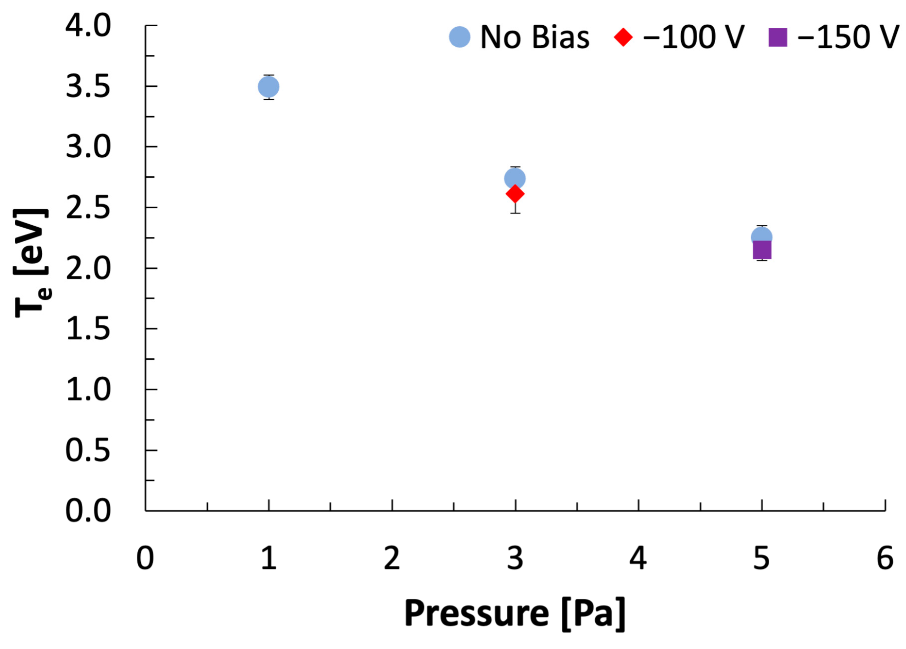
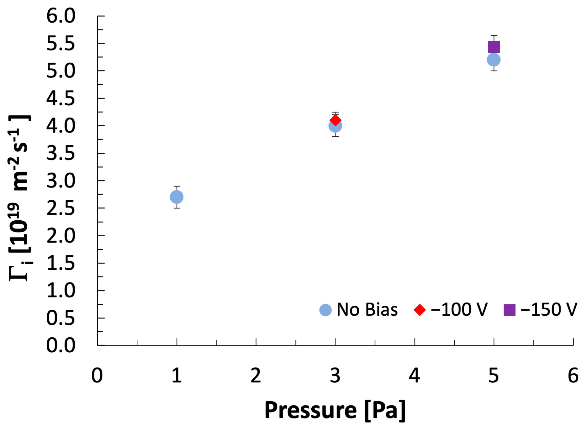
3.1. Plasma Characterization
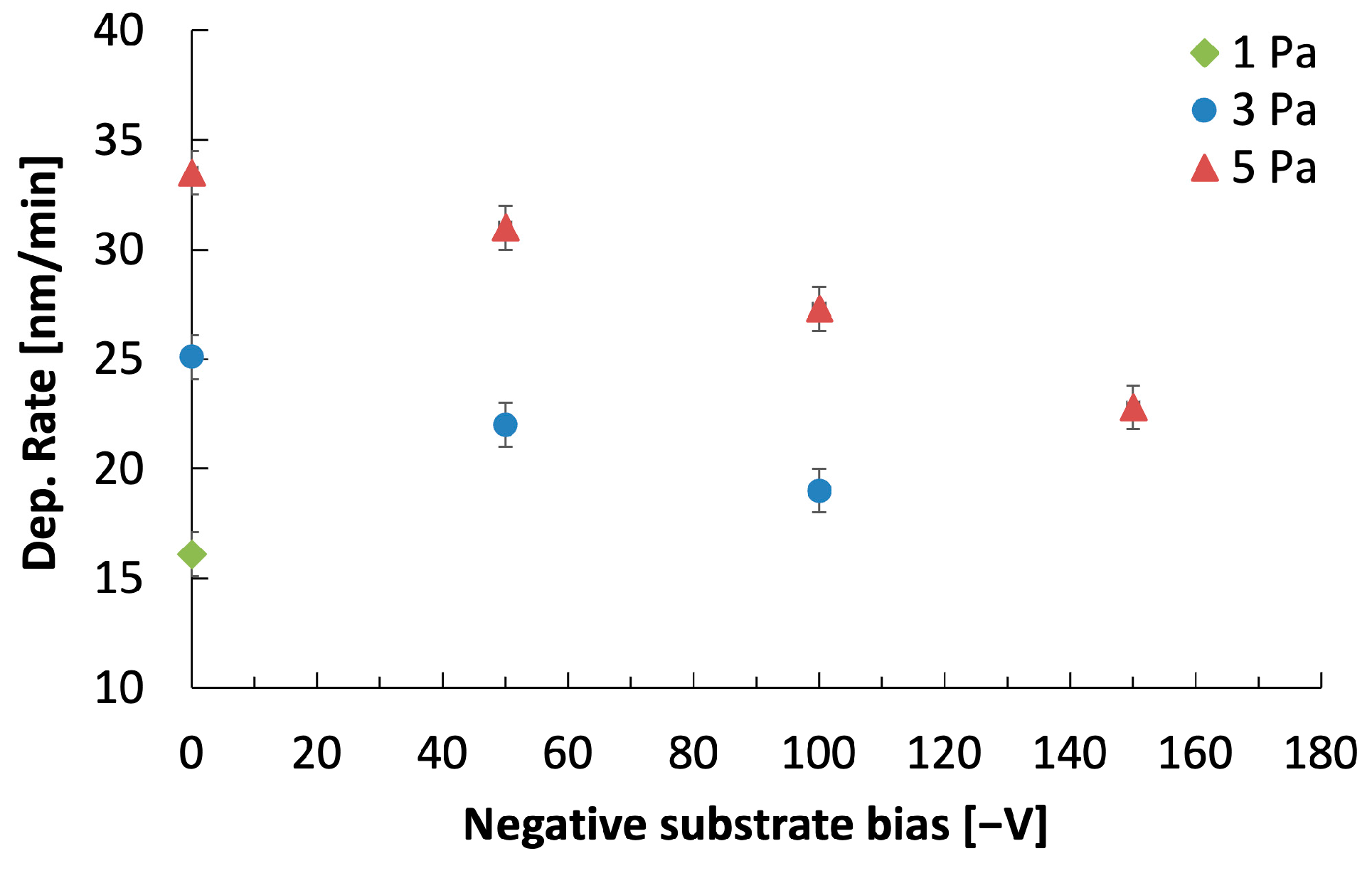
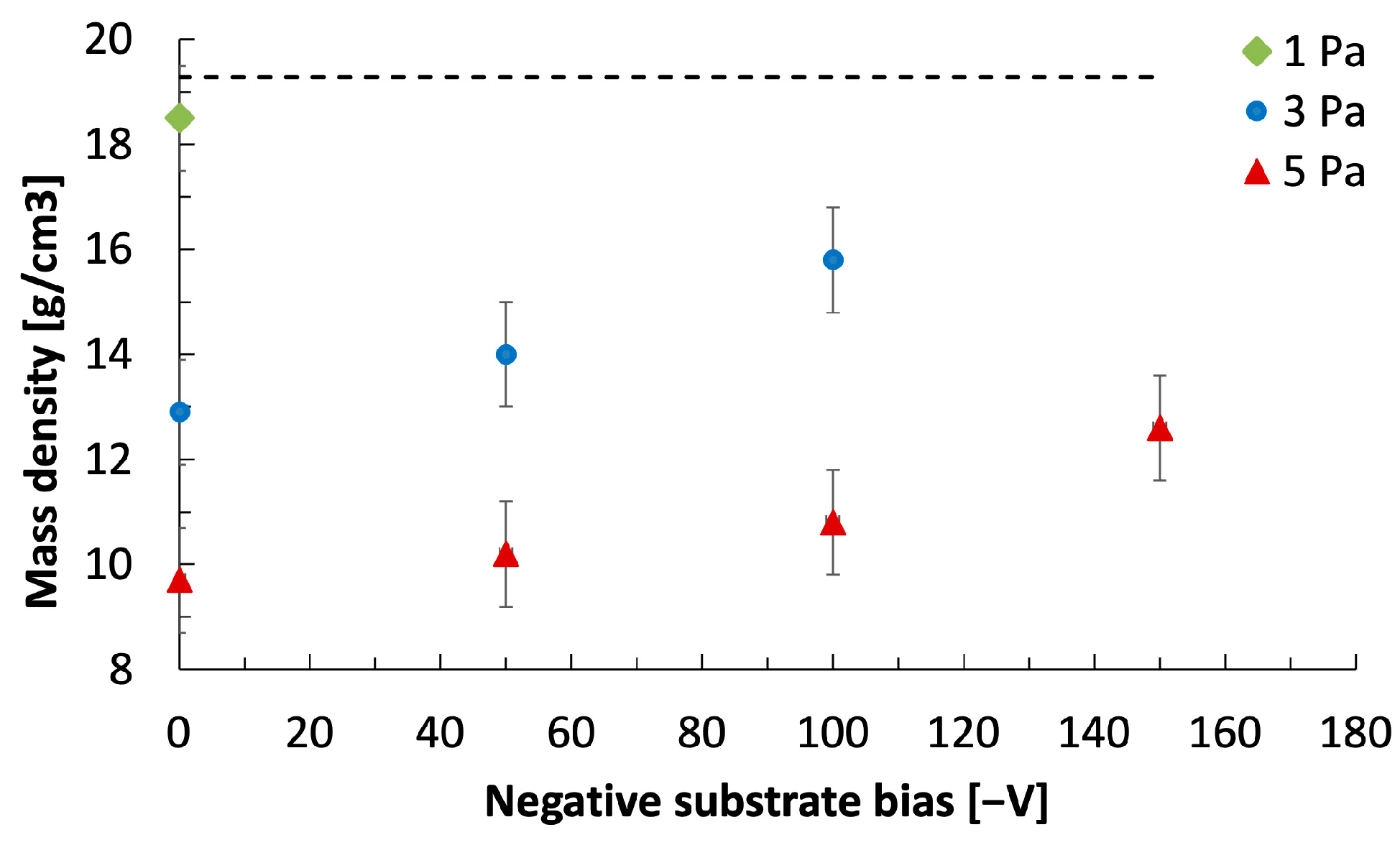
3.2. Characterization of the As-Deposited Films
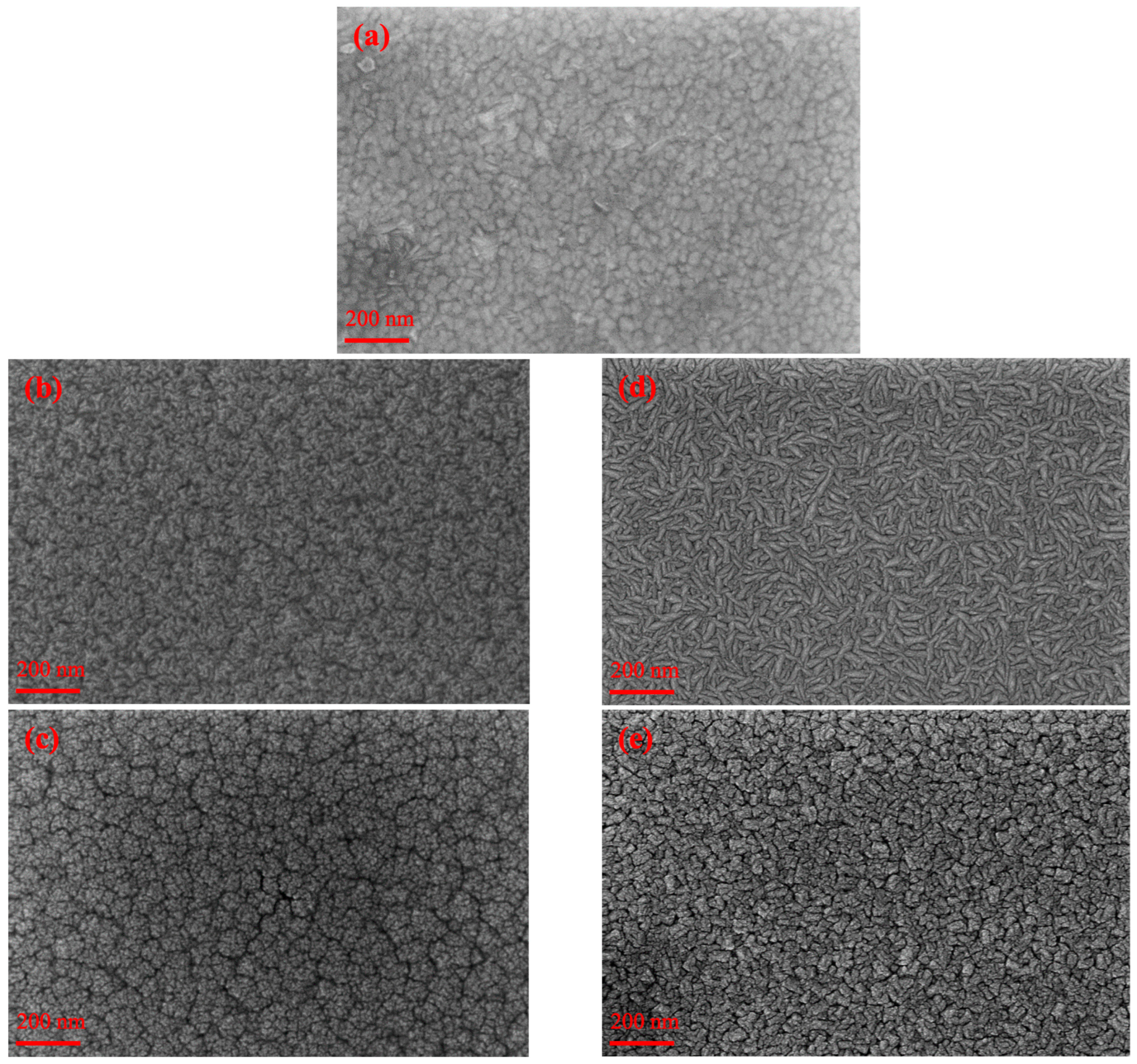
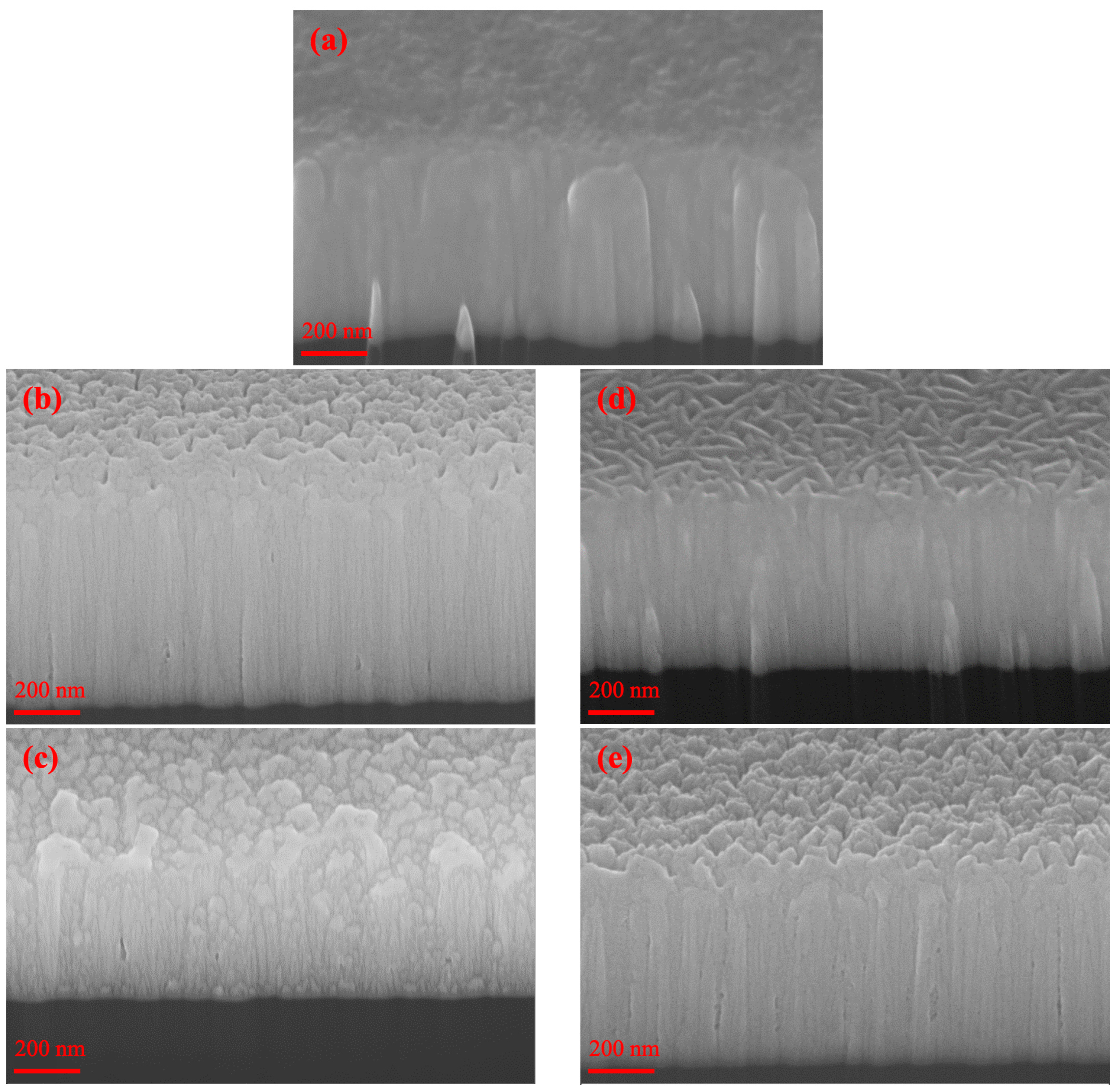
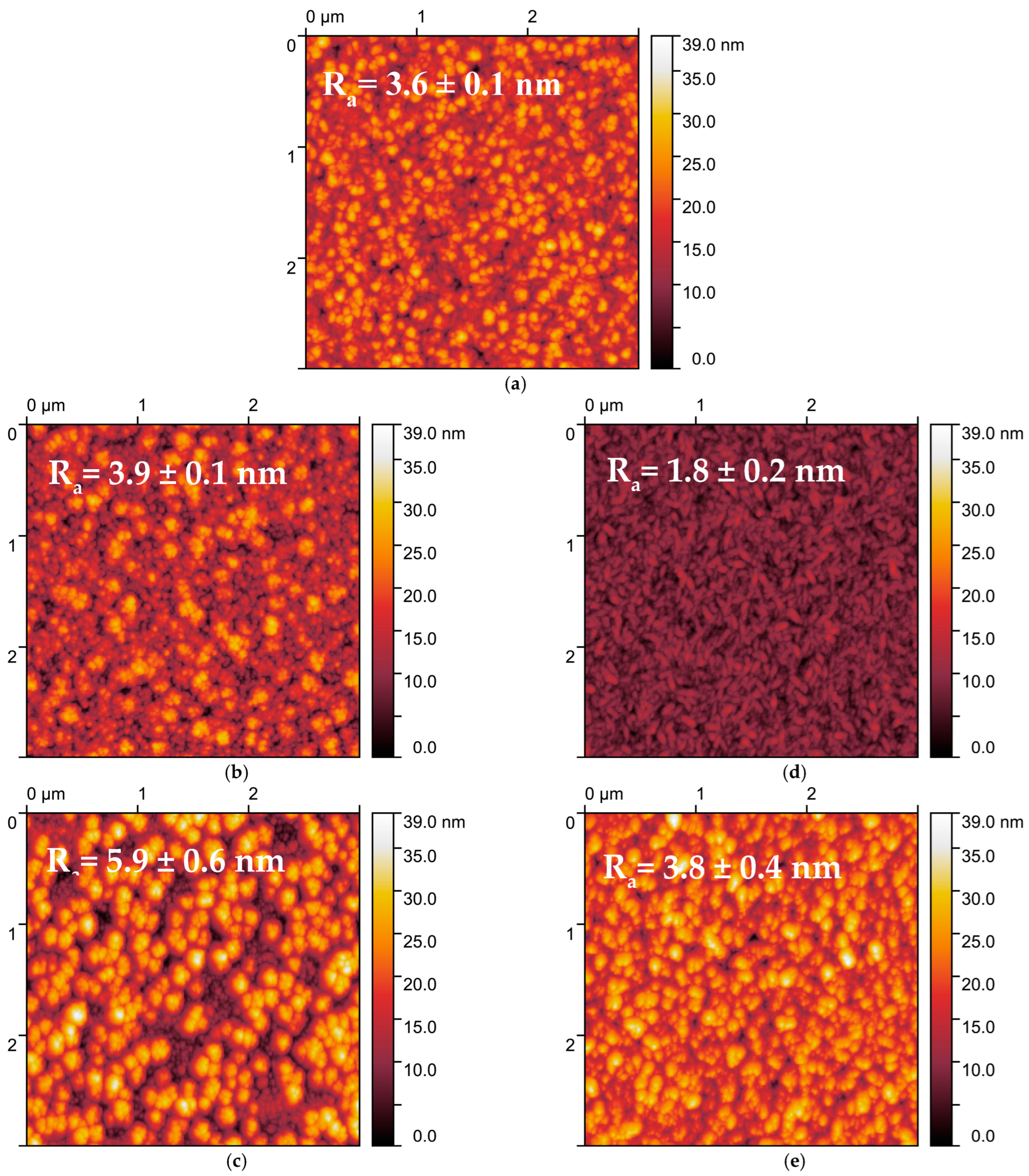
3.2.1. Surface Morphology and Microstructural Characterization (SEM, AFM and XRD)
3.2.2. Elemental Compositional Analysis
3.2.3. Electrical Resistivity
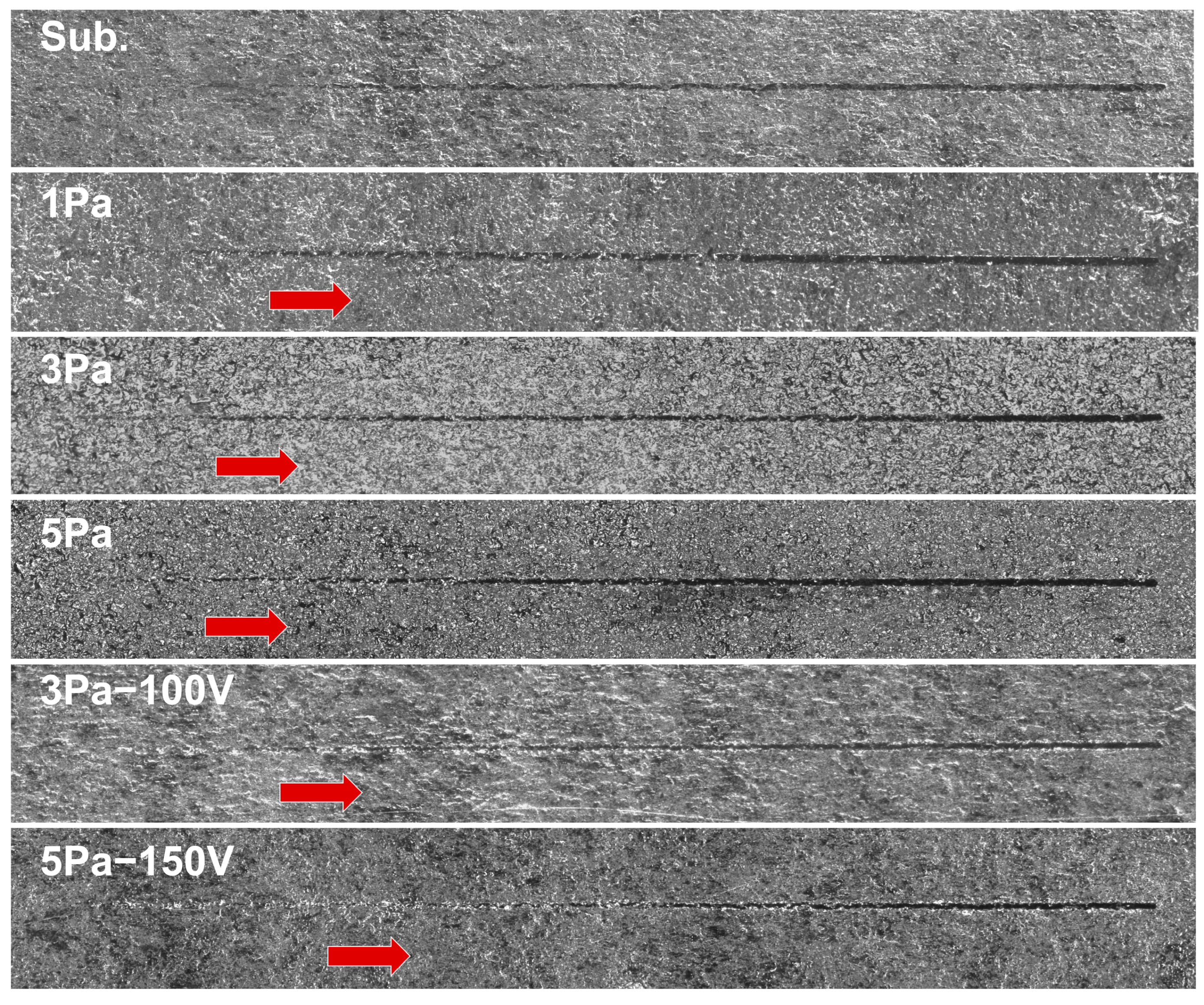
3.2.4. Mechanical Properties
4. Conclusions
Author Contributions
Funding
Institutional Review Board Statement
Informed Consent Statement
Data Availability Statement
Conflicts of Interest
References
- Lassner, E.; Schubert, W.-D. Tungsten: Properties, Chemistry, Technology of the Element, Alloys, and Chemical Compounds; Springer: New York, NY, USA, 1999. [Google Scholar]
- Rollinson, C.L. The Chemistry of Chromium, Molybdenum, and Tungsten; Pergamon Press: New York, NY, USA, 1975. [Google Scholar]
- Raumann, L.; Coenen, J.W.; Riesch, J.; Mao, Y.; Gietl, H.; Höschen, T.; Linsmeier, C.; Guillon, O. Modeling and validation of chemical vapor deposition of tungsten for tungsten fiber reinforced tungsten composites. Surf. Coat. Technol. 2020, 381, 124745. [Google Scholar] [CrossRef]
- Yeh, W.K.; Chen, M.C.; Wang, P.J.; Liu, L.M.; Lin, M.S. Deposition properties of selective tungsten chemical vapor deposition. Mater. Chem. Phys. 1996, 45, 284–287. [Google Scholar] [CrossRef]
- Dellasega, D.; Merlo, G.; Conti, C.; Bottani, C.E.; Passoni, M. Nanostructured and amorphous-like tungsten films grown by pulsed laser deposition. J. Appl. Phys. 2012, 112, 084328. [Google Scholar] [CrossRef]
- Souk, J.H.; O’Hanlon, J.F.; Angillelo, J. Characterization of electron-beam deposited tungsten films on sapphire and silicon. J. Vac. Sci. Technol. A 1985, 3, 2289–2292. [Google Scholar] [CrossRef]
- Shen, Y.G.; Mai, Y.M.; Zhang, Q.C.; McKenzie, D.R.; McFall, W.D.; McBride, W.R. Residual stress, microstructure, and structure of tungsten thin films deposited by magnetron sputtering. J. Appl. Phys. 2000, 87, 177–187. [Google Scholar] [CrossRef]
- Xu, Y.F.; Xu, Y.; Luo, L.M.; Zan, X.; Wu, Y.C. Manufacturing of magnetron sputtering tungsten coatings and irradiation damage behaviour under helium plasma exposure. Vacuum 2022, 205, 111411. [Google Scholar] [CrossRef]
- Abdelhameed, A.H.; Angloher, G.; Bauer, P.; Bento, A.; Bertoldo, E.; Canonica, L.; Fuchs, D.; Hauff, D.; Ferreiro Iachellini, N.; Mancuso, M.; et al. Deposition of tungsten thin films by magnetron sputtering for large-scale production of tungsten-based transition-edge sensors. J. Low Temp. Phys. 2020, 199, 401–407. [Google Scholar] [CrossRef]
- Verbrugghe, N.; Fasquelle, D.; Duponchel, B.; Députier, S. Study of tungsten films deposited by DC sputtering dedicated to integrated heaters. J. Vac. Sci. Technol. B 2017, 35, 031204. [Google Scholar] [CrossRef]
- Bouziane, K.; Mamor, M.; Meyer, F. DC magnetron sputtered tungsten: W film properties and electrical properties of W/Si Schottky diodes. Appl. Phys. A 2005, 81, 209–215. [Google Scholar] [CrossRef]
- Chen, G.S.; Yang, L.C.; Tian, H.S.; Hsu, C.S. Evaluating substrate bias on the phase-forming behavior of tungsten thin films deposited by diode and ionized magnetron sputtering. Thin Solid Films 2005, 484, 83–89. [Google Scholar] [CrossRef]
- Vijaya, G.; Muralidhar Singh, M.; Krupashankara, M.S.; Kulkarni, R.S. Effect of Argon Gas Flow Rate on the Optical and Mechanical Properties of Sputtered Tungsten Thin Film Coatings. IOP Conf. Ser. Mater. Sci. Eng. 2016, 149, 012075. [Google Scholar] [CrossRef]
- Chargui, A.; El Beainou, R.; Mosset, A.; Euphrasie, S.; Potin, V.; Vairac, P.; Martin, N. Influence of Thickness and Sputtering Pressure on Electrical Resistivity and Elastic Wave Propagation in Oriented Columnar Tungsten Thin Films. Nanomaterials 2020, 10, 81. [Google Scholar] [CrossRef] [PubMed]
- Zhu, L.; Li, G.; Wang, H.; Xu, B.; Zhuang, D.; Liu, J. Microstructures and nano mechanical properties of the metal tungsten film. Curr. Appl. Phys. 2009, 9, 510–514. [Google Scholar] [CrossRef]
- Maier, J.L.H.; Balden, M.; Linke, J.; Koch, F.; Bolt, H. Properties of tungsten coatings deposited onto fine grain graphite by different methods. Surf. Coat. Technol. 2001, 142-144, 733–737. [Google Scholar] [CrossRef]
- O’Keefe, M.J.; Grant, J.T.; Solomon, J.S. Magnetron sputter deposition of A-15 and bcc crystal structure tungsten thin films. J. Electron. Mater. 1995, 24, 961–967. [Google Scholar] [CrossRef]
- Zheng, P.; Ozsdolay, B.D.; Gall, D. Epitaxial growth of tungsten layers on MgO(001). J. Vac. Sci. Technol. A 2015, 33, 061505. [Google Scholar] [CrossRef]
- Rane, G.K.; Menzel, S.; Gemming, T.; Eckert, J. Microstructure, electrical resistivity and stresses in sputter deposited W and Mo films and the influence of the interface on bilayer properties. Thin Solid Films 2014, 571, 1–8. [Google Scholar] [CrossRef]
- Conrads, H.; Schmidt, M. Plasma generation and plasma sources. Plasma Sources Sci. Technol. 2000, 9, 441–454. [Google Scholar] [CrossRef]
- Smith, D.L. Thin Film Deposition: Principles and Practice; McGraw-Hill: New York, NY, USA, 1995. [Google Scholar]
- Amos, R.S.; Breyer, P.E.; Huang, H.H.; Lichtenberger, A.W. Stress and source conditions of DC magnetron sputtered Nb films. IEEE Trans. Appl. Supercond. 1995, 5, 2326–2329. [Google Scholar] [CrossRef]
- Xie, Q.; Fu, Z.; Wei, X.; Li, X.; Yue, W.; Kang, J.; Zhu, L.; Wang, C.; Meng, J. Effect of substrate bias current on structure and properties of CrNx films deposited by plasma enhanced magnetron sputtering. Surf. Coat. Technol. 2019, 365, 134–142. [Google Scholar] [CrossRef]
- Cao, F.; Munroe, P.; Zhou, Z.; Xie, Z. Influence of substrate bias on microstructural evolution and mechanical properties of TiAlSiN thin films deposited by pulsed-DC magnetron sputtering. Thin Solid Films 2017, 639, 137–144. [Google Scholar] [CrossRef]
- Ding, J.C.; Wang, Q.M.; Liu, Z.R.; Jeong, S.; Zhang, T.F.; Kim, K.H. Influence of bias voltage on the microstructure, mechanical and corrosion properties of AlSiN films deposited by HiPIMS technique. J. Alloys Compd. 2019, 772, 112–121. [Google Scholar] [CrossRef]
- Hajihoseini, H.; Kateb, M.; Ingvarsson, S.; Gudmundsson, J.T. Effect of substrate bias on properties of HiPIMS deposited vanadium nitride films. Thin Solid Films 2018, 663, 126–130. [Google Scholar] [CrossRef]
- Zenga, Y.; Tana, Z.; Zhou, L.; Jianga, M.; Qiua, Y.; Fanga, F.; Huanga, H.; Zhanga, X.; Jiang, J. Effects of bias voltage on Fen films prepared by magnetron sputtering. Mater. Res. 2015, 18, 115–119. [Google Scholar] [CrossRef]
- Wang, Z.; Zhang, D.; Ke, P.; Liu, X.; Wang, A. Influence of substrate negative bias on structure and properties of TiN coatings prepared by hybrid HIPIMS method. J. Mater. Sci. Technol. 2015, 31, 37–42. [Google Scholar] [CrossRef]
- Fan, Q.; Guo, M.; Wu, Z.; Hao, X.; Cao, F.; Liu, Y.; Wang, T. Effects of bias voltage on the microstructure and properties of AlCrN/AlTiN nanoscale multilayer coatings. Vacuum 2023, 215, 112327. [Google Scholar] [CrossRef]
- Ahn, S.M.; Jang, G.S.; Kim, D.Y.; Hwang, N.M. Effects of substrate bias and Ar pressure on growth of α-phase in W thin films deposited by RF magnetron sputtering. Electron. Mater. Lett. 2023, 19, 298–308. [Google Scholar] [CrossRef]
- Hugon, M.C.; Varniere, F.; Agius, B.; Froment, M.; Arena, C.; Bessot, J. Stresses, microstructure and resistivity of thin tungsten films deposited by RF magnetron sputtering. Appl. Surf. Sci. 1989, 38, 269–285. [Google Scholar] [CrossRef]
- Eser, E.; Ogilvie, R.E.; Taylor, K.A. The effect of bias on d.c. and r.f. sputtered WC-Co coatings. Thin Solid Films 1980, 67, 265. [Google Scholar] [CrossRef]
- Irimiciuc, S.A.; Chertopalov, S.; Lancok, J.; Craciun, V. Langmuir probe technique for plasma characterization during pulsed laser deposition process. Coatings 2021, 11, 762. [Google Scholar] [CrossRef]
- Chen, F.F. Electric Probes. In Plasma Diagnostic Techniques; Huddlestone, R.H., Leonard, S.L., Eds.; Academic Press: New York, NY, USA, 1965; Chapter 4; pp. 113–200. [Google Scholar]
- Chen, F.F.; Chang, J.P. Langmuir Probes. In Lecture Notes on Principles of Plasma Processing; Springer: Boston, MA, USA, 2003. [Google Scholar]
- Vassallo, E.; Pedroni, M.; Aloisio, M.; Minelli, D.; Nardone, A.; Chen, H.; Pietralunga, S.M.; Stinchelli, A.; Di Fonzo, F. Study of process parameters and characteristics properties of W coatings deposited by rf plasma sputtering. J. Vac. Sci. Technol. B 2023, 41, 032802. [Google Scholar] [CrossRef]
- Chung, P.M.; Talbot, L.; Touryan, K.J. Electric Probes in Stationary and Flowing Plasma; Springer: New York, NY, USA, 1975. [Google Scholar]
- Heidenreich, J.E., III.; Paraszczak, J.R.; Moisan, M.; Suave, G. Electrostatic probe analysis of microwave plasmas used for polymer etching. J. Vac. Sci. Technol. B 1987, 5, 347–354. [Google Scholar] [CrossRef]
- Lim, S.H.N.; McKenzie, D.R.; Bilek, M.M.M. Van der Pauw method for measuring resistivity of a plane sample with distant boundaries. Rev. Sci. Instrum. 2009, 80, 075109. [Google Scholar] [CrossRef]
- Van der Pauw, L.J. A method of measuring specific resistivity and Hall effect of discs of arbitrary shape. Philips Res. Rep. 1958, 13, 1–9. [Google Scholar]
- Keithley Application Note: Making van der Pauw Resistivity and Hall Voltage Measurements Using the 4200A-SCS Parameter Analyzer—Tektronix. Available online: https://www.tek.com (accessed on 1 February 2024).
- ISO 20502:2005; Fine Ceramics (Advanced Ceramics, Advanced Technical Ceramics)—Determination of Adhesion of Ceramic Coatings by Scratch Testing. ISO: Geneva, Switzerland, 2005.
- Dodd, R.; You, S.D.; Bryant, P.M.; Bradley, J.W. Negative ion density measurements in reactive magnetron sputtering. Plasma Process. Polym. 2009, 6, S615–S619. [Google Scholar] [CrossRef]
- Lieberman, M.A.; Lichtenberg, A.J. Principles of Plasma Discharges and Materials Processing, 2nd ed.; Wiley: Hoboken, NJ, USA, 2005. [Google Scholar]
- Legorreta, J.R.; Yousif, F.B.; Fuentes, E.B.; Vázquez, F.; Valencia, H.M. Interpretations of Langmuir probe data for positive ion number density of N2O DC plasma discharge. IEEE Trans. Plasma Sci. 2014, 42, 813–819. [Google Scholar] [CrossRef]
- Chen, F.F. Introduction to Plasma Physics and Controlled Fusion, 3rd ed.; Springer: New York, NY, USA, 2015. [Google Scholar]
- Holfman, W.; Thornton, J.A. Internal stresses in sputtered chromium. Thin Solid Films 1977, 40, 355–363. [Google Scholar] [CrossRef]
- Holfman, W.; Thornton, J.A. The compressive stress transition in Al, V, Zr, Nb and W metal films sputtered at low working pressures. Thin Solid Films 1977, 45, 387–396. [Google Scholar] [CrossRef]
- Holfman, W.; Thornton, J.A. Effects of substrate orientation and rotation on internal stresses in sputtered metal films. J. Vac. Sci. Technol. 1979, 16, 134–137. [Google Scholar] [CrossRef]
- Thornton, J.A.; Tabock, J.; Holfman, W.O. Internal stresses in metallic films deposited by cylindrical magnetron sputtering. Thin Solid Films 1979, 64, 111–119. [Google Scholar] [CrossRef]
- Holfman, W.; Thornton, J.A. Compressive stress and inert gas in Mo films sputtered from a cylindrical-post magnetron with Ne, Ar, Kr, and Xe. J. Vac. Sci. Technol. 1980, 17, 380–383. [Google Scholar] [CrossRef]
- Holfman, W.; Thornton, J.A. Internal stresses in Cr, Mo, Ta, and Pt films deposited by sputtering from a planar magnetron source. J. Vac. Sci. Technol. 1982, 20, 355–358. [Google Scholar] [CrossRef]
- Hoffman, D.W. Stress and property control in sputtered metal films without substrate bias. Thin Solid Films 1983, 107, 353–358. [Google Scholar] [CrossRef]
- Vüllers, F.T.N.; Spolenak, R. Alpha- vs. beta-W nanocrystalline thin films: A comprehensive study of sputter parameters and resulting materials’ properties. Thin Solid Films 2015, 577, 26–34. [Google Scholar] [CrossRef]
- Lee, M.K.; Kang, H.S. Characteristics of TiN film deposited on stellite using reactive magnetron sputter ion plating. J. Mater. Res. 1997, 12, 2393–2400. [Google Scholar] [CrossRef]
- Salamon, K.; Milat, O.; Radic, N.; Dubcek, P.; Jercinovic, M.; Bernstorff, S. Structure and morphology of magnetron sputtered W films studied by x-ray methods. J. Phys. D Appl. Phys. 2013, 46, 095304. [Google Scholar] [CrossRef]
- Maissel, L.I.; Glang, R. Handbook of Thin Film Technology; McGraw–Hill: New York, NY, USA, 1970. [Google Scholar]
- Brandes, E.A.; Brook, G.B. Smithells Metals Reference Book, 7th ed.; Butterworth-Heinemann: Oxford, UK, 1992. [Google Scholar]
- Lin, J.; Sproul, W.D.; Moore, J.J.; Wu, Z.L.; Lee, S.L. Effect of negative substrate bias voltage on the structure and properties of CrN films deposited by modulated pulsed power (MPP) magnetron sputtering. J. Phys. D Appl. Phys. 2011, 44, 425305. [Google Scholar] [CrossRef]
- Shen, Y.G.; Mai, Y.W. Influences of oxygen on the formation and stability of A15 β-W thin films. Mater. Sci. Eng. A 2000, 284, 176–183. [Google Scholar] [CrossRef]
- Ahangarani Farahani, F.; Depla, D. Phase composition of sputter deposited tungsten thin films. Surf. Coat. Technol. 2024, 494, 131447. [Google Scholar] [CrossRef]
- Weerasekera, I.A.; Shah, S.I.; Baxter, D.V.; Unruh, K.M. Structure and stability of sputter deposited beta-tungsten thin films. Appl. Phys. Lett. 1994, 64, 3231–3233. [Google Scholar] [CrossRef]
- Desai, P.D.; Chu, T.K.; James, H.M.; Ho, C.Y. Electrical resistivity of selected elements. J. Phys. Chem. Ref. Data 1984, 13, 1069–1096. [Google Scholar] [CrossRef]


| Sputtering Pressure [Pa] | Element | Element [Wt %] | ±SD |
|---|---|---|---|
| 1 | W | 99.47 | 1.05 |
| O | 0.53 | 0.10 | |
| 3 | W | 96.60 | 0.91 |
| O | 3.40 | 0.17 | |
| 5 | W | 96.10 | 1.10 |
| O | 3.90 | 0.20 |
| 1 Pa | 3 Pa | 5 Pa | 3 Pa −100 V | 5 Pa −150 V | |
|---|---|---|---|---|---|
| Lc3 (N) | 2.0 ± 0.1 | 1.7 ± 0.3 | 1.6 ± 0.1 | 2.2 ± 0.4 | 2.7 ± 0.2 |
Disclaimer/Publisher’s Note: The statements, opinions and data contained in all publications are solely those of the individual author(s) and contributor(s) and not of MDPI and/or the editor(s). MDPI and/or the editor(s) disclaim responsibility for any injury to people or property resulting from any ideas, methods, instructions or products referred to in the content. |
© 2025 by the authors. Licensee MDPI, Basel, Switzerland. This article is an open access article distributed under the terms and conditions of the Creative Commons Attribution (CC BY) license (https://creativecommons.org/licenses/by/4.0/).
Share and Cite
Vassallo, E.; Pedroni, M.; Saleh, M.; Minelli, D.; Firpo, G.; Miorin, E.; Deambrosis, S.M.; Zin, V.; Ripamonti, D.; Origo, L. Effect of Negative Substrate Bias Voltage and Pressure on the Structure and Properties of Tungsten Films Deposited by Magnetron Sputtering Technique. Coatings 2025, 15, 319. https://doi.org/10.3390/coatings15030319
Vassallo E, Pedroni M, Saleh M, Minelli D, Firpo G, Miorin E, Deambrosis SM, Zin V, Ripamonti D, Origo L. Effect of Negative Substrate Bias Voltage and Pressure on the Structure and Properties of Tungsten Films Deposited by Magnetron Sputtering Technique. Coatings. 2025; 15(3):319. https://doi.org/10.3390/coatings15030319
Chicago/Turabian StyleVassallo, Espedito, Matteo Pedroni, Miriam Saleh, Daniele Minelli, Giuseppe Firpo, Enrico Miorin, Silvia Maria Deambrosis, Valentina Zin, Dario Ripamonti, and Luca Origo. 2025. "Effect of Negative Substrate Bias Voltage and Pressure on the Structure and Properties of Tungsten Films Deposited by Magnetron Sputtering Technique" Coatings 15, no. 3: 319. https://doi.org/10.3390/coatings15030319
APA StyleVassallo, E., Pedroni, M., Saleh, M., Minelli, D., Firpo, G., Miorin, E., Deambrosis, S. M., Zin, V., Ripamonti, D., & Origo, L. (2025). Effect of Negative Substrate Bias Voltage and Pressure on the Structure and Properties of Tungsten Films Deposited by Magnetron Sputtering Technique. Coatings, 15(3), 319. https://doi.org/10.3390/coatings15030319