Article

The Amorphous Carbon Layers Deposited by Various Magnetron Sputtering Techniques

by
Rafal Chodun
1,*,
Lukasz Skowronski
2,
Marek Trzcinski
2,
Dobromil Zaloga
3,
Katarzyna Nowakowska-Langier
3,
Piotr Domanowski
4 and
Krzysztof Zdunek
1
1
Faculty of Materials Science and Engineering, Warsaw University of Technology, 02-507 Warsaw, Poland
2
Department of Surface Science, Faculty of Chemical Technology and Engineering, Bydgoszcz University of Science and Technology, 85-796 Bydgoszcz, Poland
3
National Centre for Nuclear Research (NCBJ), 05-400 Otwock, Poland
4
Faculty of Mechanical Engineering, Bydgoszcz University of Science and Technology, 85-796 Bydgoszcz, Poland
*
Author to whom correspondence should be addressed.
Coatings 2025, 15(12), 1367; https://doi.org/10.3390/coatings15121367 (registering DOI)
Submission received: 29 October 2025 / Revised: 17 November 2025 / Accepted: 20 November 2025 / Published: 22 November 2025

Abstract

This study investigates the synthesis and characterization of amorphous carbon (a-C) layers using three magnetron sputtering (MS) techniques: Pulsed MS (PMS), Gas Injection MS (GIMS), and High Power GIMS (HiPGIMS). The primary objective was to understand how these methods influence the sp3/sp2 hybridization ratio, a critical parameter for tailoring the properties of amorphous carbon. Plasma diagnostics via Optical Emission Spectroscopy revealed distinct discharge characteristics, with HiPGIMS exhibiting the highest current density and plasma ionization. Structural and compositional analyses using Raman Spectroscopy and X-ray Photoelectron Spectroscopy (XPS) demonstrated a clear trend: sp3 content increased significantly from PMS to GIMS to HiPGIMS, reaching up to 50% (Raman) and 39% (XPS). This enhancement is attributed to the higher plasma density and more energetic ion bombardment in HiPGIMS, which promotes the formation of sp3 bonds. Ellipsometric spectroscopy further supported these findings, showing that HiPGIMS produced layers with the widest bandgap, indicative of higher sp3 content. The research highlights the effectiveness of advanced MS techniques, particularly HiPGIMS, in precisely controlling the sp3/sp2 ratio and thereby the electrical, optical, and mechanical properties of a-C layers for various applications.

1. Introduction

Amorphous carbon (a-C) layers are incredibly versatile materials that are important in industry and scientific research [1]. Their unique properties, including exceptional hardness [2], low friction [3], excellent chemical inertness [4], and biocompatibility [5], make them ideal for a wide range of applications. a-C layers are extensively used to enhance the performance and lifespan of mechanical components, tools, and medical implants.
Scientifically, the tunable nature of a-C allows for the exploration of novel electronic and optical properties [6]. This tunability stems from the varying ratios of sp2 and sp3 hybridized carbon atoms within the amorphous structure [7]. This control enables the development of advanced materials for sensors [8,9], microelectronics [6,10], and energy storage devices [11,12]. Furthermore, their inertness makes them valuable as protective layers in harsh chemical environments [13,14] and as substrates for advanced biological studies [15,16].
The ability to tailor their characteristics makes amorphous carbon layers a cornerstone for innovation across diverse scientific and industrial frontiers. The properties of a-C layers are profoundly influenced by the relative proportion of sp3/sp2 bonding between carbon atoms [17]. The sp3 tetrahedral bonding dictates the layer’s hardness, density, and high elastic modulus. Conversely, sp2-bonded carbon contributes to the layer’s graphitic character, which in turn influences its electrical conductivity and optical absorption. Therefore, the sp3/sp2 ratio is a critical parameter in tailoring a-C layers for specific applications, allowing for the precise control of their mechanical, electrical, and optical characteristics, ranging from hard, diamond-like layers to more flexible, graphite-like layers.
The a-C layers can be deposited using various methods, each offering unique advantages and characteristics. Among the most common techniques are Magnetron Sputtering (MS) [18,19], Plasma-Enhanced Chemical Vapor Deposition [20,21], Laser Ablation [22,23], Filtered Cathodic Vacuum Arc [24,25], and Arc Deposition [26,27], among others. There is noticeable interest in using the MS techniques for a-C layers synthesis. This is due to the high scalability of the MS for industrial production, the high uniformity of the layers, and its high sensitivity to deposition conditions. This sensitivity enables the tailoring of the layers’ characteristics, chemical composition, phase composition, and structural features. In the context of a-C layers, controlling the sp3/sp2 ratio is crucial. Several technological MS parameters control the sp3/sp2 ratio, including sputtering pressure [28,29], substrate temperature [30,31], substrate bias [32,33], sputtering gas [34,35], and power density [36,37], among others. The explanation behind the sp3/sp2 ratio is the active role of ions during the phase and structure formation of the layer. A common concept in the literature concerns the shallow implantation of energetic species (up to 100 eV) in an amorphous sp2 carbon matrix. This model assumes that energetic species transfer their kinetic energy into reconfiguring the surrounding atoms during penetration, creating the sp3 hybridized volume of the matrix [38,39]. This mechanism is primarily expected to occur under conditions favoring rather low dissipation of the kinetic energy in inelastic collisions with cold gas molecules and/or with the substrate under negative biasing. The other mechanism explaining the formation of the sp3 phase is the homogeneous nucleation on ions as the crystallization centers [40,41]. This mechanism suggests that valence electrons in carbon clusters can be significantly excited through non-elastic collisions with plasma electrons. The excitation of these electrons favors the creation of sp3 bonds at the expense of sp2 bonds. The ultrasmall clusters prevent phonon excitations, so the energy exchanged can be used to create the metastable phase. After reaching the surface of the substrate, the clusters form a sp3-rich carbon film.
In this work, we wanted to address the issue of synthesizing a-C layers using various magnetron sputtering techniques but utilizing common apparatus components. Thus, it is important to have the ability to analyze the results of layer deposition resulting from different methods of plasma excitation and their propagation conditions. For this purpose, we used the following techniques:
  • Pulsed Magnetron Sputtering (PMS)—a technique that can be considered a technological standard of MS, characterized by a low degree of plasma component excitation and a power density in the range of 100–102 W/cm2 [42,43];
  • Gas Injection Magnetron Sputtering (GIMS)—a technique that uses power pulses with a density characteristic of the PMS technique but coupled with the operation of pulsed valves supplying working gas [44,45]. Thanks to this, the generated plasma pulses have a chance to propagate in an environment with a lower concentration of gas molecules, which leads to limiting the dissipation of plasma particle energy [46,47];
  • High Power Gas Injection Magnetron Sputtering (HiPGIMS)—pulsed technique using short power pulses with a density of around 102–103 W/cm2, coupled with the operation of pulsed valves supplying working gas [37] and characterized by a high degree of excitation of plasma components [48,49,50].
All MS versions were implemented in a common vacuum chamber, the same pumping system, gas dosing apparatus, magnetron gun, and graphite target. Glow discharges of each SM process were diagnosed to evaluate the plasma excitation state. The deposited layers were examined both structurally and in terms of phase composition, with a particular focus on determining the sp3/sp2 ratio. Additionally, optical properties were examined to estimate the electronic structure of the fabricated a-C layers.

2. Materials and Methods

2.1. Sputtering the Graphite Targets

Figure 1 presents a diagram of the three different MS techniques used in the experiment: PMS, GIMS, and HiPGIMS. All the process parameters are gathered and presented in Table 1. The 5 × 10⁻⁴ Pa base pressure in the chamber was established by a vacuum system comprising turbomolecular, Roots, and rotary pumps. The constant Ar atmosphere was created to perform the PMS process of a-C layers deposition. The mid-frequency DPS power supply (PS) (Dora Power Systems, Wroclaw, Poland) [51] (Posadowski et al., 2008) was used for PMS sputtering of a 5 cm diameter and 4 mm thick graphite target (purity 99.97%). The target was sputtered with an average current density of 14 mA/cm2 and a power density of 10 W/cm2.
The fast impulse gas valve (GV) system coupled with DPS PS was used to perform the GIMS process. The Ar was used as a sputtering gas and delivered through the outlet directed at the magnetron target. The GV operation parameters were adjusted by the electronic controller and are listed in Table 1: the opening time (tAr) and frequency (T). The controller was also coupled with PS, allowing for setting the power pulse ignition and turning it off. For this experiment, the 50 ms power pulses (tpulse) were used to deposit a-C films.
The duty cycle D of GIMS was 10%. Jdmean was calculated and equaled 23 mA/cm2 while Pdmean was 18 W/cm2. The pulse manner of gas distribution, with parameters described above, resulted in periodic pressure fluctuations (pAr) ranging from 10−3 to 10−1 Pa, in contrast to the PMS process’s pressure, which is fixed at 0.4 Pa.
The DPS high-power supply was used to perform the HIPGIMS process. The DPS HiPS was coupled with the GV system to create the same pressure oscillating conditions as the GIMS process: the opening time (tAr) and frequency (T). Under these conditions, the system generated 1 ms long plasma pulses with a Jdmean of 74 mA/cm2 and a Pdmean of 6 W/cm2. The D was 0.2%. The tpulse was the only technological parameter different from the GIMS process, which was an effect of the electronic construction of the DPS HiPS.
The a-C layers were fabricated onto Si (100) wafers, which were mounted perpendicularly to the Z axis of the magnetron at a distance of 80 mm from the target, as a result of the (tproc) deposition process. The wafers were cleaned by ultrasonic treatment in acetone for 15 min and then dried before being mounted in the vacuum chamber. The deposition process did not involve any intentional substrate biasing or heating. The deposition temperature did not exceed 60 °C.

2.2. Examination Methods

Plasma characterization was performed by analyzing the magnetron electric circuit’s current and voltage waveforms, as well as using optical emission spectroscopy (OES). The current and voltage waveforms were measured using a 1 A: 0.1 V Rogowski coil and a 1 kV: 1 V voltage probe (Dora Power Systems, Wroclaw, Poland), and recorded by a Rigol MSO5204 oscilloscope (Rigol Technologies Inc., Portland, OR, USA). All calculations were performed using OriginLab software (2019b ver. 9.6.5.169). OES investigations were executed using a Mechelle 900 optical spectrometer (Oxford Instruments Andor, Belfast, UK) with a mounted SensiCam Fs camera (300–1000 nm spectral range, relative spectral resolution ∆λ/λ = 900. The 100 ms (PMS and GIMS) and 10 ms (HiPGIMS) exposition frames were used to register the generated plasma’s OES spectra. Plasma spectra were registered during 100, 200, and 500 exposure frames for PMS, GIMS, and HiPGIMS, respectively. A high number of frames was crucial for achieving a satisfactory signal-to-noise ratio and for obtaining the most statistically representative plasma spectrum under the investigated conditions. Registration was triggered from a current rise measured by a Rogowski coil mounted in the magnetron cathode’s electric circuit. Exposition time was 100 (PMS and GIMS) or 10 ms (HiPGIMS) long. Spectra registration was performed by the optical collimator (Oxford Instruments Andor, Belfast, UK), which was positioned 80 mm from the cathode surface. The collimator was oriented parallel to the magnetron’s cathode surface. The intensity of registered OES spectra was further normalized considering various numbers of frames and exposure times.
The structure morphology of the 5 μm × 5 μm surface area of the a-C films was imaged using Atomic Force Microscopy (AFM) by an Innova device (Bruker Corp., Billerica, MA, USA). The investigation was conducted using the tapping mode. The analysis was performed using the Gwyddion software (ver. 2.61, GNU, Brno, Czech Republic). The surface roughness (Sa) has been calculated using Equation (1):
S a =   1 A A z x ,   y d x d y
where A and z(x, y) are the best-fitting mean plane and the height of the surface relative to A, respectively.
X-ray Photoelectron Spectroscopy (XPS) was used to examine the composition and sp3/sp2 ratio of the a-C films. The film samples were investigated in an ultra-high vacuum of ≤2 × 10⁻¹⁰ mbar. A lamp with an Al K-α aluminum anode (1486.6 eV) (Prevac, Rogow, Poland) was used as a source of the excitation radiation for the spectrometer. The photoelectron energy was measured using a VG-Scienta R3000 analyzer (VG-Scienta, Uppsala, Sweden) with a ΔE = 0.1 eV step. The experimental data were calibrated with respect to the position of the C1s level and fitted to Gauss-Lorentz shapes using Casa XPS software (ver. 2.3.17, Casa Software Ltd., Teignmouth, UK).
The vibrational spectroscopy of the a-C layers was studied using a 532 nm VIS laser (2.33 eV) and a 266 nm UV laser (4.66 eV). The Ar+ laser and the Crylas FQCW266-50 (CryLaS GmbH, Berlin, Germany) diode-pumped continuous-wave solid-state laser were used as the VIS and UV excitation sources, respectively. The scattered light was detected by a JASCO NRS-5100 spectrometer (JASCO International Co., Ltd., Tokyo, Japan), operating in backscattering mode. The ~20 μm spots of film samples were investigated. The registration conditions were optimized based on the satisfactory signal-to-noise ratio. The Spectra Manager Micro Imaging Analysis v.2.3 (JASCO, Tokyo, Japan) and Curve Fitting v.1.9 (JASCO, Tokyo, Japan) processing software were used to analyze the registered spectra. The spectra were processed by interpolation and background subtraction, aligning levels at each side of the presented range. The curve fitting operation determined the position and a full width at half maximum FWHM of the peaks D and G. The sp3 bond content was calculated based on the G peak dispersion rate [52]. The sp3/sp2 ratio, as the G peak dispersion is expressed by Equations (2) and (3):
s p c o n t e n t 3 =   0.07 + 2.5   ×   D i s p G   ± 0.06
D i s p G = P o s G @ λ 1 P o s G @ λ 2 λ 1 λ 2
where P o s G @ λ 1 and P o s G @ λ 2 are the G peak positions at λ 1 and λ 2 irradiation, respectively. λ 1 and λ 2 are the laser wavelength.
The ellipsometric azimuths ψ and Δ have been measured from 190 nm (6.5 eV) to 2000 nm (0.6 eV) for 65°, 70°, and 75° incidence. The Spectroscopic ellipsometry (SE) measurements were performed using the V-VASE device from J.A.Woollam Co., Ltd. (Lincoln, NE, USA). The ψ and Δ ellipsometric azimuths are defined as Equation (4) [53,54]:
ρ ~ =   tan ψ e x p i
where ρ ~ is the ratio of the amplitude reflection of the electromagnetic radiation for p and s polarization, and i   is the imaginary unit.
The WASE32 software (version 3.774) was used for further analysis. The refractive index n and extinction coefficient k optical constants were determined this way. Based on the k , the absorption coefficient α was calculated using Equation (5):
α =   4 π k λ
where λ is the wavelength of the incident light. The energy band gap of the layers was determined using the Tauc method [55,56]. This is based on the assumption that the energy-dependent absorption coefficient α can be expressed by Equation (6):
( α × h ν ) 1 / m = B ( h ν   E g )
where h ν is the photon energy, and B is a constant. The m factor depends on the nature of the electron transition and corresponds to 0.5, 1.5, 2, or 3 for the direct allowed, direct forbidden, indirect allowed, and indirect forbidden transition band gaps, respectively. Our experiment obtained the most linear curves for the indirect allowed transition ( m = 2). A linear fit procedure was used to extrapolate the linear parts of the plots. The bandwidths, Eg were read from the extrapolated lines that intersected the X-axis.

3. Results and Discussion

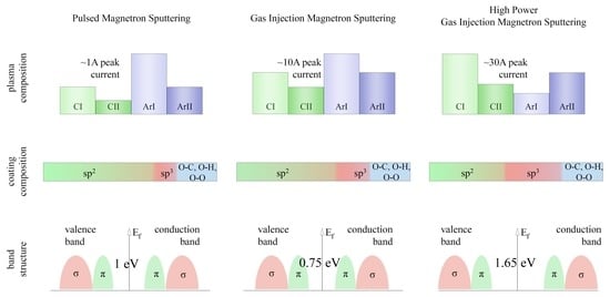
Figure 2 presents the current and voltage waveforms of the glow discharge generated in every process investigated in the experiment. The characteristics indicate differences in the nature of the discharge. The PMS is characterized by a relatively low 0.2 A average current, 14 mA/cm2 average current density (Jdmean), and a 10 W/cm2 power density (Pdmean). Due to the characteristics of graphite, i.e., low sputtering yield, high ionization energy of carbon atoms, and graphite structure, it is impossible to generate a discharge characterized by high power density without using an additional approach to assist sputtering and ionization. In the case of the GIMS process, the maximum current peak was registered as ~10 A. We have also noticed a significant improvement in the density of Jdmean and Pdmean, at 23 mA/cm2 and 18 W/cm2, respectively. Since the plasma is initiated by the injection of the working gas portion into the high-vacuum interelectrode space, it is possible to obtain high current values (higher ionization than in PMS) by reducing the kinetic energy dissipation of excited plasma species. The high current peak is ~1.5 ms long, and after this period, the plasma appears to become thermalized, resulting in a current level comparable to that observed in the PMS method. The full length of the plasma pulse was measured to be 50 ms. The HiPGIMS process demonstrates an approach to raise the Jdmean more than GIMS. The HiPGIMS combines the advantages of working gas injections with the use of a high-power source. The effect was ~30 A, with a current peak lasting 0.3 ms. The Jdmean increased to 74 mA/cm2, and the Pdmea was calculated as 6 W/cm2. The relatively low Pdmean compared to the other processes is due to the short HiPGIMS pulse duration (1ms HiPGIMS vs. 50 ms GIMS). Since the power density was averaged over the 500 ms period to calculate the Pdmean, the Pdmean does not adequately reflect the significance of the HiPGIMS process. To present the key difference between the power peak of GIMS and HiPGIMS, the power density was calculated based solely on the power peak. The power density at its peak was 254 W/cm2 for GIMS and 1274 W/cm2 for HiPGIMS, respectively.
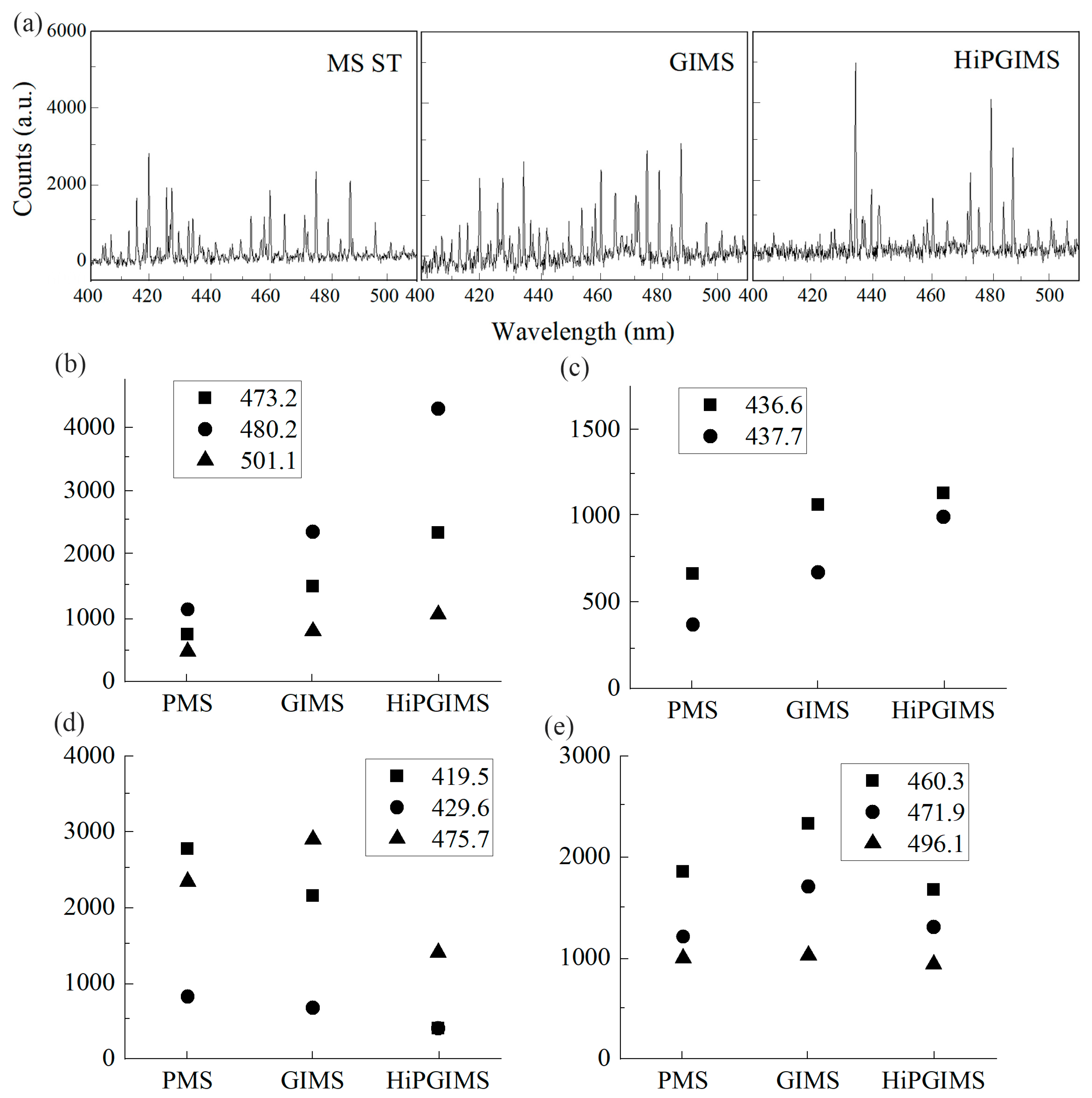
These significant differences in plasma pulses should be reflected in the composition of OES spectra. In Figure 3, the results of OES investigations are presented. Figure 3a presents a comparison of the individual spectral characteristics for each examined process. The detailed information on the assigned spectral lines is presented in Table 2.
The intensities of the spectra were normalized according to the various exposure times and the number of exposure frames. Although the intensities of the optical emission lines do not directly indicate the species population in the plasma, the trend of line intensity evolution within each species group can provide valuable information on the plasma content as the process version changes [57]. Trends are observed for a specific group of plasma constituents. In Figure 3b), we present the chosen normalized intensities of the lines of the C I species. The population of sputtered and excited C I carbon atoms seems to expand as the generated plasma is expected to be more ionized. We have observed the same trend for carbon ions (C II-Figure 3c). The trend is opposite in the case of gaseous-originated plasma constituents, excited Ar I (Figure 3d) species, and Ar II ions (Figure 3e). It demonstrates the positive role of utilizing the pulse action of a gas dosing valve, which limits the population of Ar excited species to the amount required to generate the discharge, and achieves the carbon vapors through sputtering. An excess population of excited gas plasma species (represented by a process with a constant concentration of working gas–PMS) does not yield positive results in the number of ionized plasma constituents. Interestingly, the lowest intensity of ionized Ar II was observed for HiPGIMS, while the highest was for GIMS. It can be explained by the reversed movement of ions generated by HiPGIMS due to a strong electric field in the magnetic trap region, which is oriented towards the target [58,59]. It is a common phenomenon for high-power MS techniques, and its effect creates a potential barrier that traps ions near the target, preventing them from reaching the substrate/OES collimator zone.
Figure 4 shows the morphology of the a-C films’ surface. There are not many differences between the films observed. All films exhibit dense and smooth surface characteristics for films deposited with a significant number of ions. The calculated roughness S a was about ~0.5 nm.
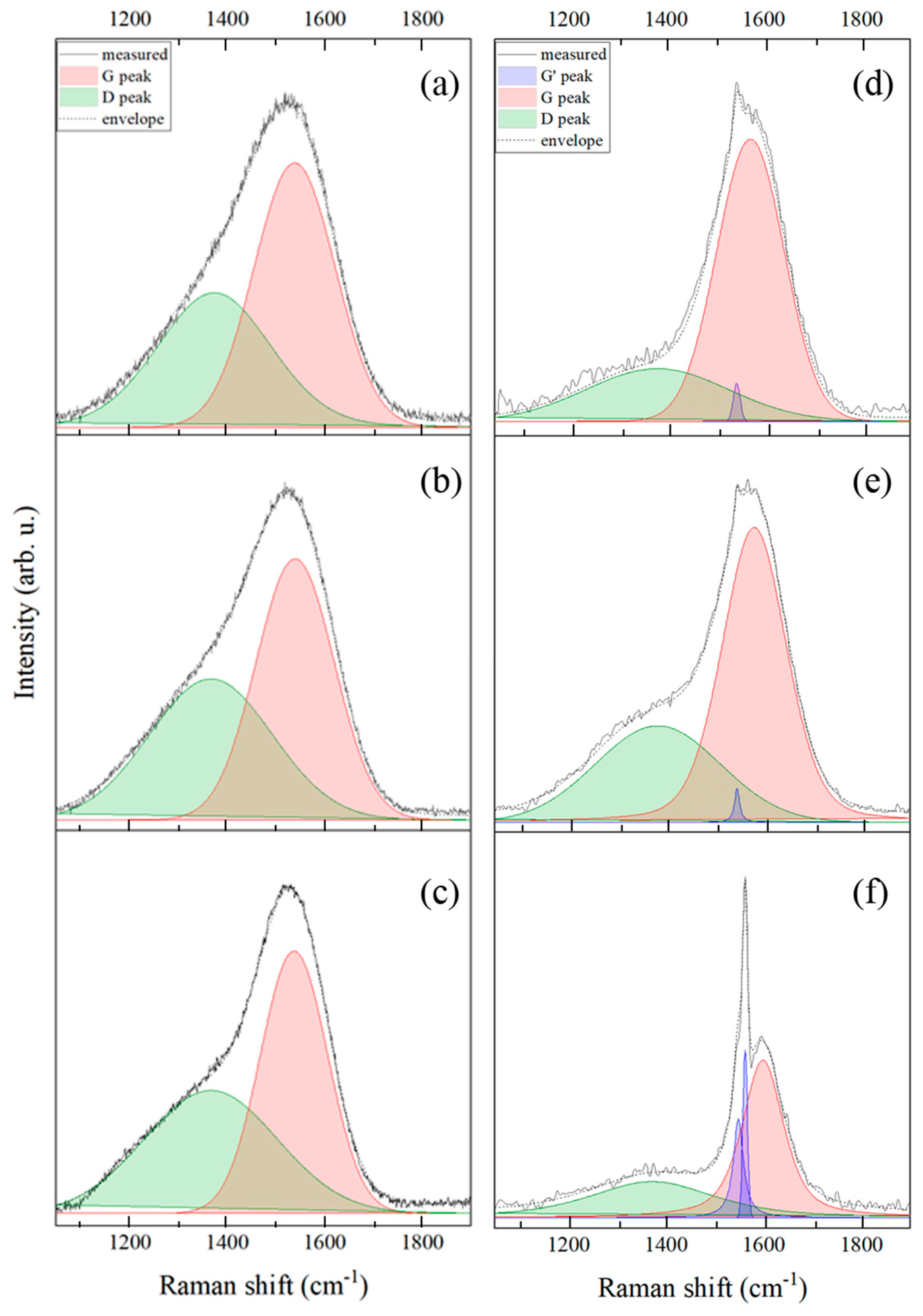
To evaluate the sp3/sp2 ratio, the a-C layers were examined by Raman spectroscopy. Monocrystal graphite exhibits a ~1580 cm−1 Raman active band E2g, labeled G (Graphite). The G peak affects the stretching vibration of the sp2 sites. With the graphite amorphization, an additional mode at ~1350 cm−1, A1g, appears, known as the D peak (Disorder). The D mode is attributed to the breathing modes of the sp2 sites in rings. According to the Ferrari diagram of 3-stage carbon amorphization [60], the sp3 bond is expected when the in-plane correlation length Ls is below 2 nm [61]. Correctly determining the characteristics of the G and D peaks (positions, intensity, and FWHM) from the a-C Raman spectra is reported as the method of evaluating the sp3 bond content. Figure 5 presents the Raman spectra of a-C layers collected under VIS and UV laser irradiation, as well as the effects of G and D mode fitting. Evaluated parameters of fitted peaks are shown in Table 3. The ~0.5 ratio of D peak to G peak intensity, the 160–200 cm−1 FWHM of G peak, and ~1538 cm−1 of G peak position suggest that 10–50% of sp3 content is expected [60,61,62]. To quantitatively evaluate the sp3/sp2 ratio, a method based on the dispersion of the G peak was used [52,63]. The ratio was calculated using Equation (2).
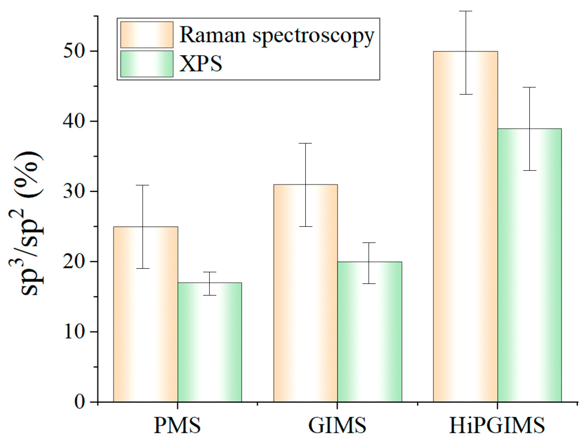
Figure 6 shows the calculated sp3/sp2 ratio from Raman spectroscopy and the XPS method. Despite the differences in the calculated ratio by both methods, a noticeable common trend of increasing sp3 is observed. The sp3 was evaluated as 25 ± 6, 31 ± 6, and 50 ± 6% for PMS, GIMS, and HiPGIMS, respectively (Raman spectroscopy approach), and 17 ± 2, 20 ± 3, and 39 ± 6% (XPS approach). In summary, more sp3 was obtained in high-current discharges. This is because the increased current results in a higher plasma density. This, in turn, provides more energetic ions that bombard the growing layer. These energetic ions can effectively promote the formation of sp3 bonds [37,64,65].
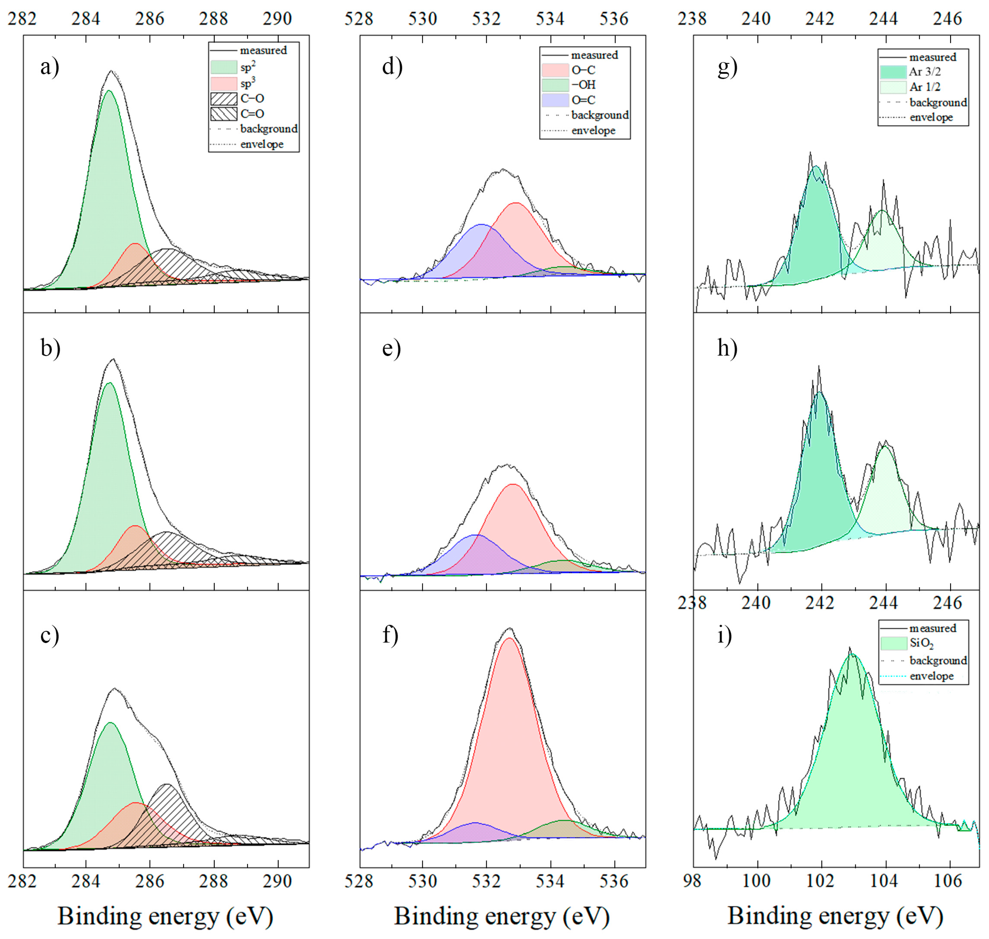
The differences in sp3 content between the experimental methods used likely stem from obstacles to accurately evaluating oxygen influence on Raman spectra of a-C films. The XPS method seems to be more precise than Raman spectroscopy. The second explanation is the fact that the surface region of a-C layers is enriched in sp2 bonds [66]. Therefore, an XPS study, which examines only the material at its surface (a few nanometers), always shows an increased sp2 content compared to methods that are sensitive to material features detected at a greater depth. Raman spectroscopy is an example of such a method. Films fabricated in the experiment were <50 nm thin, so Raman spectroscopy provided the spectroscopic information from the entire depth of the film, in contrast to XPS. Figure 7 shows the C1s and O1s core levels of a-C layers deposited by MS techniques. Additionally, a small amount of Ar was detected in the composition of the PMS and GIMS layers, as represented by the Ar2p orbital. The Si was observed in the chemical composition of HiPGIMS a-C layer (represented by Si2p core level). The detailed chemical composition of the deposited layers is shown in Table 4. The main components of the C1s core level are carbon peaks originating from sp2- and sp3-hybridized bonds, at 284.6 and 285.5 eV, respectively [67,68]. The C1s level incorporates additional C–O bonds on the surface, and carbonyl bonds (C=O) [67]. These levels were determined at binding energies of 286.3 and 288.8 eV, respectively. The O1s orbital incorporates three elementary components: O–C component at 532.8 eV, carbonyl O=C component at 531.5 eV, and O–H component at 534.6 eV [69]. The Ar2p orbital was present in the XPS spectra of PMS and GIMS layers. The measured argon 2p level consists of the Ar2p3/2 sublevel at 241.8 eV and Ar2p1/2 at 244.2 eV [70]. The Ar contamination of the layer structures is reported and studied in the literature. The total amount of working gas trapped in the layer structure may depend on the ion energy and flux to the substrate, which can be controlled by the shape, amplitude, and duration of the voltage and current pulses [71,72]. In the case of a-C layers deposited in our experiment, Ar was detected during the process, characterized by an increased content of Ar I and Ar II plasma species (see Figure 3d,e).
In the case of the HiPGIMS process, where the population of Ar species was evaluated as relatively low compared to other MS processes, no Ar2p core level was measured. The Si2p orbital was detected in the HiPGIMS layer with a SiO2 component at 103.0 eV [73]. In our opinion, the presence of Si atoms is the effect of partial sputtering and recondensation of the substrate surface at the initial stage of carbon layer deposition. The sputtering process can be efficient in the HiPGIMS process since it is recognized as the most energetic in terms of the degree of ionization of the plasma.
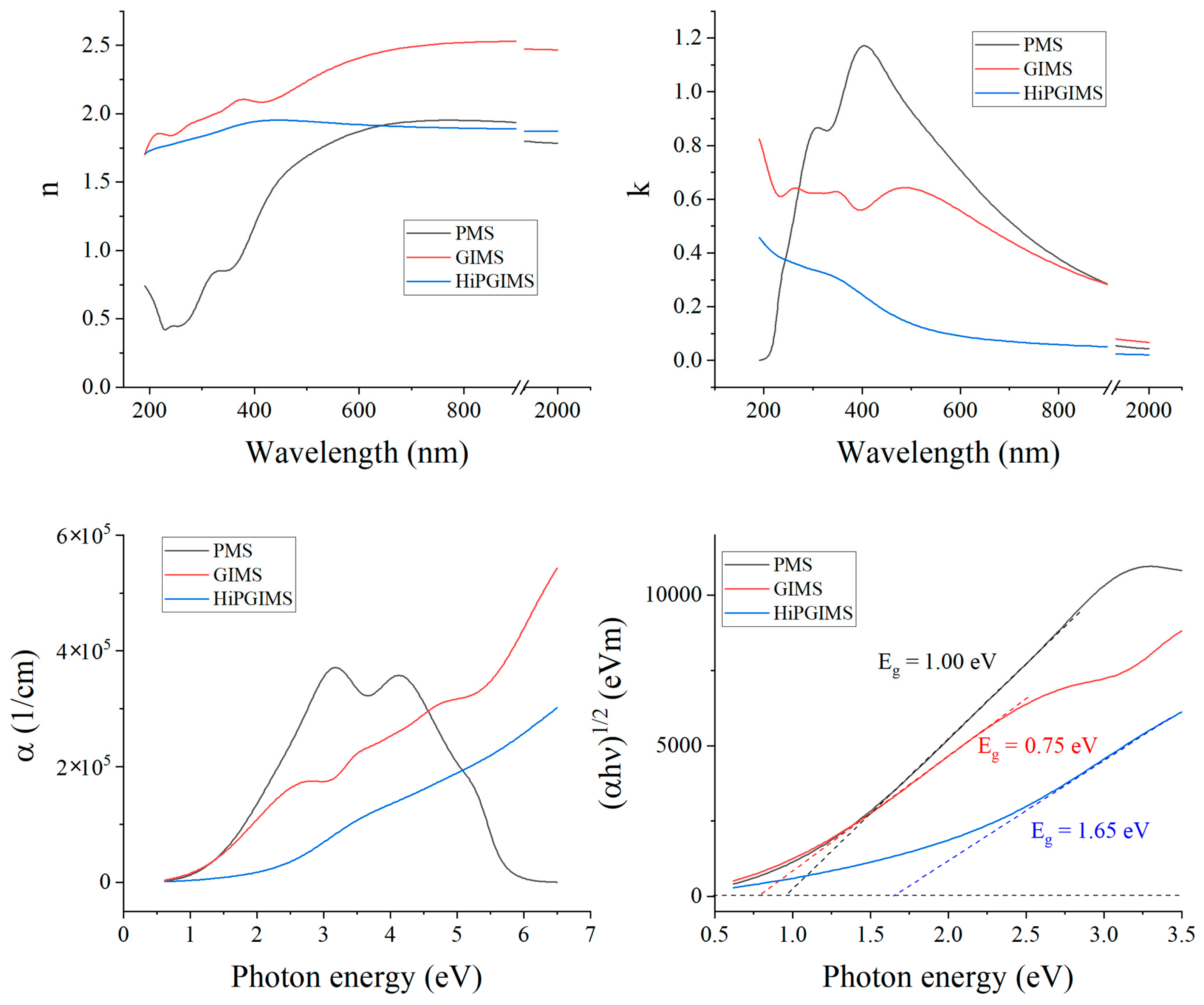
Spectroscopic ellipsometry was used to examine the optical properties of a-C layers and to determine their thickness. The thickness was determined to be 16.4 ± 0.1, 35.4 ± 0.5, and 34.3 ± 0.4 nm for PMS, GIMS, and HiPGIMS, respectively. Calculated deposition rate was: 16 Å/min (PMS), 2.95 Å/min (GIMS-10% duty cycle), and 2.86 Å/min (HiPGIMS-0.2% duty cycle). This is an expected trend, based on the increased effects of sputtering, measured as current density and the population of carbon species, as registered by OES in GIMS and HiPGIMS techniques. The optical constants (refractive index—n and the extinction coefficient—k), absorption coefficient α, and Tauc plots ( α h ν ) 1 / 2 are shown in Figure 8. PMS and the other processes have a difference in the shape of n. For UV, the n value takes very low values, ranging from 0.5 to 1.0. With the λ increase in the VIS range, the n significantly increases to 1.8 and remains at that level to the IR spectral range. This specific n shape is characteristic of low-density carbon materials, especially those rich with sp2 clusters [74,75]. The k of a-C layer synthesized by PMS is also characteristic of sp2 carbon, exhibiting a strong maximum in the visible range and low values in the UV and IR regions [74]. The n and k plots for layers fabricated using the other process are similar for dense carbon materials, contributing a significant content of the sp3 phase [74]. This conclusion is supported by the previously presented results, which indicate that the GIMS and HiPGIMS processes favor the synthesis of the sp3 phase, in contrast to the PMS.
The α plot exhibits similar features to k. The plot of the PMS process exhibits characteristic features for low-density carbon, where absorption rises in the IR region (~1 eV) and the UV region (~5.5 eV). The absorption region of a-C layers deposited by other methods is wider and characteristic of carbon materials, exhibiting an increased content in the sp3 phase [74].
The Tauc plots show differences in the electron structure of deposited a-C layers. The calculated bandgap energy (Eg) is presented as 1.00 ± 0.03, 0.75 ± 0.02, and 1.65 ± 0.03 eV for PMS, GIMS, and HiPGIMS, respectively. The highest value of Eg presents the layer that contributes the highest amount of sp3–HiPGIMS. None of the layers presents a sharp edge of absorption. It means that there is a significant influence of π π transition characteristic for the sp2 phase of carbon.
In the context of the analyzed magnetron sputtering techniques, a clear relationship exists between the measured plasma parameters and the obtained sp3/sp2 hybridization ratio. The PMS technique was characterized by the lowest average current density (14 mA/cm2) and average power density (10 W/cm2), resulting in the generation of a relatively low ionized plasma. Neither the subplantation mechanism nor homogeneous nucleation of metastable phases such as sp3-hybridized carbon is favored by such a plasma environment. As a result, the carbon film with the lowest sp3 was deposited. In the case of GIMS, an increase in the average current density to 23 mA/cm2 and average power density to 18 W/cm2 was observed, with a peak power of 254 W/cm2, resulting in the creation of a more energetic plasma environment. An increase in ions and a decrease in the working gas’s unionized species were observed. The only difference from PMS was the pulsating mechanism of gas dosing, which created favorable conditions for preserving kinetic energy by the plasma species. This resulted in a higher sp3 content in the deposited film. A sp3 increase in relation to PMS is not significant: from 25 ± 6 to 31 ± 6% (according to Raman spectroscopy) and from 17 ± 2 to 20 ± 3% (according to XPS). Despite a 1.5 ms strong current peak of the GIMS discharge, a significant part of it (48.5 ms) consists of a low-current part, resembling the PMS process. This results in the plasma composition becoming potentially complex over time, and the material of the deposited film can also be complex, exhibiting characteristics of both carbon phases formed in a low-ionization environment (sp2) and those formed in a high-ionization environment (sp3). The HiPGIMS showed the highest average current density (74 mA/cm2) and a significantly higher peak power density (1274 W/cm2), which was associated with the highest degree of plasma ionization. The most intense spectral lines of ions of sputtered atoms. These more energetic plasma conditions in HiPGIMS resulted in the highest sp3 content in the films, as determined by Raman (50 ± 6%) and XPS (39 ± 6%) measurements. Similar to GIMS, the current characteristic consists of high- and low-current parts, resulting in the formation of both sp3 and sp2 carbon phases. In the case of HiPGIMS, the peak power density is significantly higher, and the low-current part is similar in length to the high-current part; therefore, the significant content of sp3 was measured in this film. In summary, increased current and power density, and consequently, higher plasma density and more energetic ion bombardment, effectively promote the formation of sp3 bonds, which are crucial for controlling the properties of amorphous carbon layers.

4. Conclusions

This study successfully investigated the synthesis and characterization of a-C layers deposited using three distinct MS techniques: PMS, GIMS, and HiPGIMS. The primary objective was to elucidate the influence of these deposition methods on the critical sp3/sp2 hybridization ratio, which dictates the material’s properties.
Plasma diagnostics, particularly OES, revealed significant differences in discharge characteristics, with HiPGIMS exhibiting the highest current density and plasma ionization. Structural and compositional analyses, employing Raman Spectroscopy and XPS, consistently demonstrated a clear trend: the sp3 content progressively increased from PMS to GIMS and reached its maximum in HiPGIMS layers, achieving values of up to 50 ± 6% (Raman) and 39 ± 6% (XPS). This enhanced sp3 bonding is directly attributed to the higher plasma density and more energetic ion bombardment inherent in the HiPGIMS process. Further corroboration came from ellipsometric spectroscopy, which showed that HiPGIMS-deposited layers possessed the widest bandgap, which indicates higher sp3 content. It appears that there is still some margin for increasing the sp3 content, which would provide greater control over the current pulse, particularly the elimination of the low-current component that is most likely responsible for the deposition of the sp2 fraction. Alternatively, specific effects could be achieved by using pulsed biasing of the substrate, adapted to the dynamically changing temporal structure of the generated plasma. The proper application of both the first and second methods requires further research, especially in deepening the characterization of the temporal-spatial nature of plasma pulses in GIMS and HiPGIMS methods.
In summary, this research highlights the superior capability of advanced MS techniques, particularly HiPGIMS, in precisely controlling the sp3/sp2 ratio within amorphous carbon layers. The ability to tune this fundamental structural parameter offers a robust pathway for tailoring the mechanical, electrical, and optical properties of a-C films, thereby expanding their potential for diverse technological applications.

Author Contributions

Conceptualization, R.C. and K.Z.; methodology, R.C. and K.Z.; software, R.C., L.S. and M.T.; validation, R.C., L.S., M.T. and K.N.-L.; formal analysis, R.C., L.S., M.T.; investigation, R.C., L.S., M.T., D.Z. and K.N.-L.; resources, P.D. and D.Z.; data curation, R.C., L.S., M.T., P.D. and D.Z.; writing—original draft preparation, R.C.; writing—review and editing, R.C., L.S. and M.T.; visualization, R.C.; supervision, K.Z. and R.C.; project administration, R.C.; funding acquisition, R.C. All authors have read and agreed to the published version of the manuscript.

Funding

This research was funded by Warsaw University of Technology’s Scientific Disciplines Councils, Grant No.504/04931/1090/43.082401.

Institutional Review Board Statement

Not applicable.

Informed Consent Statement

Not applicable.

Data Availability Statement

Dataset available upon request to the authors.

Acknowledgments

The authors thank Mieczyslaw Naparty of the Faculty of Chemical Technology and Engineering from Bydgoszcz University of Science and Technology for conducting the AFM measurements.

Conflicts of Interest

The authors declare no conflict of interest.

References

  1. Rajak, D.K.; Kumar, A.; Behera, A.; Menezes, P.L. Diamond-Like Carbon (DLC) Coatings: Classification, Properties, and Applications. Appl. Sci. 2021, 11, 4445. [Google Scholar] [CrossRef]
  2. Kulkarni, A.V.; Bhushan, B. Nanoindentation measurements of amorphous carbon coatings. J. Mater. Res. 1997, 12, 2707–2714. [Google Scholar] [CrossRef]
  3. Li, L.; Song, W.; Ovcharenko, A.; Xu, M.; Zhang, G. Effects of atomic structure on the frictional properties of amorphous carbon coatings. Surf. Coat. Technol. 2015, 263, 8–14. [Google Scholar] [CrossRef]
  4. Bhushan, B. Chemical, mechanical and tribological characterization of ultra-thin and hard amorphous carbon coatings as thin as 3.5 nm: Recent developments. Diam. Relat. Mater. 1999, 8, 1985–2015. [Google Scholar] [CrossRef]
  5. Grill, A. Diamond-like carbon coatings as biocompatible materials—An overview. Diam. Relat. Mater. 2003, 12, 166–170. [Google Scholar] [CrossRef]
  6. Kim, I.-S.; Shim, C.-E.; Kim, S.W.; Lee, C.-S.; Kwon, J.; Byun, K.-E.; Jeong, U. Amorphous Carbon Films for Electronic Applications. Adv. Mater. 2023, 35, 2204912. [Google Scholar] [CrossRef]
  7. Robertson, J. Structure and Electronic Properties of Diamond-Like Carbon. In Diamond and Diamond-like Films and Coatings; Clausing, R.E., Horton, L.L., Angus, J.C., Koidl, P., Eds.; Springer: New York, NY, USA, 1991; pp. 331–356. [Google Scholar] [CrossRef]
  8. Saparina, S.V.; Kharintsev, S.S. Amorphous Carbon Thin Films for Optical Sensing of Humidity. Bull. Russ. Acad. Sci. Phys. 2022, 86, S187–S190. [Google Scholar] [CrossRef]
  9. Zhou, J.; Guo, P.; Cui, L.; Yan, C.; Xu, D.; Li, F.; Zhang, C.; Wang, A. Wrinkled and cracked amorphous carbon film for high-performance flexible strain sensors. Diam. Relat. Mater. 2023, 132, 109619. [Google Scholar] [CrossRef]
  10. Silva, S.R.P.; Carey, J.D. Enhancing the electrical conduction in amorphous carbon and prospects for device applications. Diam. Relat. Mater. 2003, 12, 151–158. [Google Scholar] [CrossRef]
  11. Yaroslavtsev, A.B.; Stenina, I.A. Carbon coating of electrode materials for lithium-ion batteries. Surf. Innov. 2020, 9, 92–110. [Google Scholar] [CrossRef]
  12. Guo, T.; Hu, P.; Li, L.; Wang, Z.; Guo, L. Amorphous materials emerging as prospective electrodes for electrochemical energy storage and conversion. Chem 2023, 9, 1080–1093. [Google Scholar] [CrossRef]
  13. Yin, P.; Liu, Z.; Cao, X.; Lu, Z.; Zhang, G. Evaluation of the corrosion protection effect of amorphous carbon coating through the corrosion behaviors on different substrates. Diam. Relat. Mater. 2024, 142, 110771. [Google Scholar] [CrossRef]
  14. Li, S.; Li, H.; Guo, P.; Li, X.; Yang, W.; Ma, G.; Nishimura, K.; Ke, P.; Wang, A. Enhanced Long-Term Corrosion Resistance of 316L Stainless Steel by Multilayer Amorphous Carbon Coatings. Materials 2024, 17, 2129. [Google Scholar] [CrossRef]
  15. Roy, R.K.; Lee, K.-R. Biomedical applications of diamond-like carbon coatings: A review. J. Biomed. Mater. Res. Part B Appl. Biomater. 2007, 83B, 72–84. [Google Scholar] [CrossRef] [PubMed]
  16. Tiainen, V.-M. Amorphous carbon as a bio-mechanical coating—Mechanical properties and biological applications. Diam. Relat. Mater. 2001, 10, 153–160. [Google Scholar] [CrossRef]
  17. Robertson, J. Preparation and properties of amorphous carbon. J. Non-Cryst. Solids 1991, 137–138, 825–830. [Google Scholar] [CrossRef]
  18. Savvides, N.; Window, B. Diamond-like amorphous carbon films prepared by magnetron sputtering of graphite. J. Vac. Sci. Technol. A 1985, 3, 2386–2390. [Google Scholar] [CrossRef]
  19. Vetter, J.; Stüber, M.; Ulrich, S. Growth effects in carbon coatings deposited by magnetron sputtering. Surf. Coat. Technol. 2003, 168, 169–178. [Google Scholar] [CrossRef]
  20. Yáñez-Hernández, L.A.; Bonilla-Gameros, L.; Chevallier, P.; Sarkissian, A.; Mantovani, D. Plasma-Based Amorphous Carbon Coatings on Polymeric Substrates for Biomedical Applications: A Critical Review Focused on Adhesion. Appl. Sci. 2025, 15, 9968. [Google Scholar] [CrossRef]
  21. Che, J.; Yi, P.; Peng, L.; Lai, X. Impact of pressure on carbon films by PECVD toward high deposition rates and high stability as metallic bipolar plate for PEMFCs. Int. J. Hydrog. Energy 2020, 45, 16277–16286. [Google Scholar] [CrossRef]
  22. Voevodin, A.A.; Donley, M.S. Preparation of amorphous diamond-like carbon by pulsed laser deposition: A critical review. Surf. Coat. Technol. 1996, 82, 199–213. [Google Scholar] [CrossRef]
  23. Gaudiuso, R. Pulsed Laser Deposition of Carbon-Based Materials: A Focused Review of Methods and Results. Processes 2023, 11, 2373. [Google Scholar] [CrossRef]
  24. Hakovirta, M.; Tiainen, V.-M.; Pekko, P. Techniques for filtering graphite macroparticles in the cathodic vacuum arc deposition of tetrahedral amorphous carbon films. Diam. Relat. Mater. 1999, 8, 1183–1192. [Google Scholar] [CrossRef]
  25. Polo, M.C.; Andújar, J.L.; Hart, A.; Robertson, J.; Milne, W.I. Preparation of tetrahedral amorphous carbon films by filtered cathodic vacuum arc deposition. Diam. Relat. Mater. 2000, 9, 663–667. [Google Scholar] [CrossRef]
  26. Schultrich, B. Structure and Characterization of Vacuum Arc Deposited Carbon Films—A Critical Overview. Coatings 2022, 12, 109. [Google Scholar] [CrossRef]
  27. Schultrich, B.; Scheibe, H.-J.; Drescher, D.; Ziegele, H. Deposition of superhard amorphous carbon films by pulsed vacuum arc deposition. Surf. Coat. Technol. 1998, 98, 1097–1101. [Google Scholar] [CrossRef]
  28. Liu, J.Q.; Li, L.J.; Wei, B.; Wen, F.; Cao, H.T.; Pei, Y.T. Effect of sputtering pressure on the surface topography, structure, wettability and tribological performance of DLC films coated on rubber by magnetron sputtering. Surf. Coat. Technol. 2019, 365, 33–40. [Google Scholar] [CrossRef]
  29. Nguyen, T.; Ulrich, S.; Bsul, J.; Beauvais, S.; Burger, W.; Albers, A.; Stüber, M.; Ye, J. Influence of argon gas pressure and target power on magnetron plasma parameters. Diam. Relat. Mater. 2009, 18, 995–998. [Google Scholar] [CrossRef]
  30. Chowdhury, S.; Laugier, M.T.; Rahman, I.Z. Characterization of DLC coatings deposited by rf magnetron sputtering. J. Mater. Process. Technol. 2004, 153–154, 804–810. [Google Scholar] [CrossRef]
  31. Chowdhury, S.; Laugier, M.T.; Rahman, I.Z. Effects of substrate temperature on bonding structure and mechanical properties of amorphous carbon films. Thin Solid Film. 2004, 447–448, 174–180. [Google Scholar] [CrossRef]
  32. Ahmad, I.; Roy, S.S.; Maguire, P.D.; Papakonstantinou, P.; McLaughlin, J.A. Effect of substrate bias voltage and substrate on the structural properties of amorphous carbon films deposited by unbalanced magnetron sputtering. Thin Solid Film. 2005, 482, 45–49. [Google Scholar] [CrossRef]
  33. Nakamura, M.; Takagawa, Y.; Miura, K.; Kobata, J.; Zhu, W.; Nishiike, N.; Arao, K.; Marin, E.; Pezzotti, G. Structural alteration induced by substrate bias voltage variation in diamond-like carbon films fabricated by unbalanced magnetron sputtering. Diam. Relat. Mater. 2018, 90, 214–220. [Google Scholar] [CrossRef]
  34. Dai, W.; Gao, X.; Wang, Q.; Xu, A. Influence of Ne sputtering gas on structure and properties of diamond-like carbon films deposited by pulsed-magnetron sputtering. Thin Solid Film. 2017, 625, 163–167. [Google Scholar] [CrossRef]
  35. Sahu, B.B.; Kim, S.I.; Lee, M.W.; Han, J.G. Effect of helium incorporation on plasma parameters and characteristic properties of hydrogen free carbon films deposited using DC magnetron sputtering. J. Appl. Phys. 2020, 127, 14901. [Google Scholar] [CrossRef]
  36. Dai, W.; Li, X.; Wu, L.; Wang, Q. Influences of target power and pulse width on the growth of diamond-like/graphite-like carbon coatings deposited by high power impulse magnetron sputtering. Diam. Relat. Mater. 2021, 111, 108232. [Google Scholar] [CrossRef]
  37. Skowronski, L.; Chodun, R.; Trzcinski, M.; Zdunek, K. Optical Properties of Amorphous Carbon Thin Films Fabricated Using a High-Energy-Impulse Magnetron-Sputtering Technique. Materials 2023, 16, 7049. [Google Scholar] [CrossRef] [PubMed]
  38. Lifshitz, Y.; Kasi, S.R.; Rabalais, J.W.; Eckstein, W. Subplantation model for film growth from hyperthermal species. Phys. Rev. B 1990, 41, 10468–10480. [Google Scholar] [CrossRef] [PubMed]
  39. Lifshitz, Y.; Lempert, G.D.; Grossman, E.; Avigal, I.; Uzan-Saguy, C.; Kalish, R.; Kulik, J.; Marton, D.; Rabalais, J.W. Growth mechanisms of DLC films from C+ ions: Experimental studies. Diam. Relat. Mater. 1995, 4, 318–323. [Google Scholar] [CrossRef]
  40. Sokołowska, A.; Zdunek, K.; Grigoriew, H.; Romanowski, Z. The structure and mechanical properties of carbon layers formed by crystallization from pulse plasma. J. Mater. Sci. 1986, 21, 763–767. [Google Scholar] [CrossRef]
  41. Sokołowski, M. Influence of the pulse plasma chemical content on the crystallization of diamond under conditions of its thermodynamic instability. J. Cryst. Growth 1981, 54, 519–522. [Google Scholar] [CrossRef]
  42. Belkind, A.; Freilich, A.; Lopez, J.; Zhao, Z.; Zhu, W.; Becker, K. Characterization of pulsed dc magnetron sputtering plasmas. New J. Phys. 2005, 7, 90. [Google Scholar] [CrossRef]
  43. Vlček, J.; Pajdarová, A.D.; Musil, J. Pulsed dc Magnetron Discharges and their Utilization in Plasma Surface Engineering. Contrib. Plasma Phys. 2004, 44, 426–436. [Google Scholar] [CrossRef]
  44. Zdunek, K.; Nowakowska-Langier, K.; Chodun, R.; Dora, J.; Okrasa, S.; Talik, E. Optimization of gas injection conditions during deposition of AlN layers by novel reactive GIMS method. Mater. Sci.-Pol. 2014, 32, 171–175. [Google Scholar] [CrossRef]
  45. Skowronski, L.; Zdunek, K.; Nowakowska-Langier, K.; Chodun, R.; Trzcinski, M.; Kobierski, M.; Kustra, M.K.; Wachowiak, A.A.; Wachowiak, W.; Hiller, T.; et al. Characterization of microstructural, mechanical and optical properties of TiO2 layers deposited by GIMS and PMS methods. Surf. Coat. Technol. 2015, 282, 16–23. [Google Scholar] [CrossRef]
  46. Chodun, R.; Nowakowska-Langier, K.; Wicher, B.; Okrasa, S.; Minikayev, R.; Dypa, M.; Zdunek, K. TiO2 coating fabrication using gas injection magnetron sputtering technique by independently controlling the gas and power pulses. Thin Solid Films 2021, 728, 138695. [Google Scholar] [CrossRef]
  47. Chodun, R.; Nowakowska-Langier, K.; Wicher, B.; Okrasa, S.; Kwiatkowski, R.; Zaloga, D.; Dypa, M.; Zdunek, K. The state of coating–substrate interfacial region formed during TiO2 coating deposition by Gas Injection Magnetron Sputtering technique. Surf. Coat. Technol. 2020, 398, 126092. [Google Scholar] [CrossRef]
  48. Alami, J.; Bolz, S.; Sarakinos, K. High power pulsed magnetron sputtering: Fundamentals and applications. J. Alloys Compd. 2009, 483, 530–534. [Google Scholar] [CrossRef]
  49. Ehiasarian, A.P.; New, R.; Münz, W.-D.; Hultman, L.; Helmersson, U.; Kouznetsov, V. Influence of high power densities on the composition of pulsed magnetron plasmas. Vacuum 2002, 65, 147–154. [Google Scholar] [CrossRef]
  50. Sarakinos, K.; Alami, J.; Konstantinidis, S. High power pulsed magnetron sputtering: A review on scientific and engineering state of the art. Surf. Coat. Technol. 2010, 204, 1661–1684. [Google Scholar] [CrossRef]
  51. Posadowski, W.M.; Wiatrowski, A.; Dora, J.; Radzimski, Z.J. Magnetron sputtering process control by medium-frequency power supply parameter. Thin Solid Film. 2008, 516, 4478–4482. [Google Scholar] [CrossRef]
  52. Cui, W.G.; Lai, Q.B.; Zhang, L.; Wang, F.M. Quantitative measurements of sp3 content in DLC films with Raman spectroscopy. Surf. Coat. Technol. 2010, 205, 1995–1999. [Google Scholar] [CrossRef]
  53. Woollam, J.A. Guide to Using WVASE32®; Wextech Systems Inc.: Mendota Heights, MN, USA, 2010. [Google Scholar]
  54. Fujivara, H. Spectroscopic Ellipsometry. In Principles and Applications; John Wiley and Sons: Hoboken, NJ, USA, 2009. [Google Scholar]
  55. Tauc, J. Optical properties and electronic structure of amorphous Ge and Si. Mater. Res. Bull. 1968, 3, 37–46. [Google Scholar] [CrossRef]
  56. Tauc, J.; Grigorovici, R.; Vancu, A. Optical Properties and Electronic Structure of Amorphous Germanium. Phys. Status Solidi (B) 1966, 15, 627–637. [Google Scholar] [CrossRef]
  57. Ganesan, R.; Murdoch, B.J.; Treverrow, B.; Ross, A.E.; Falconer, I.S.; Kondyurin, A.; McCulloch, D.G.; Partridge, J.G.; McKenzie, D.R.; Bilek, M.M.M. The role of pulse length in target poisoning during reactive HiPIMS: Application to amorphous HfO2. Plasma Sources Sci. Technol. 2015, 24, 35015. [Google Scholar] [CrossRef]
  58. Kadlec, S.; Čapek, J. Return of target material ions leads to a reduced hysteresis in reactive high power impulse magnetron sputtering: Model. J. Appl. Phys. 2017, 121, 171910. [Google Scholar] [CrossRef]
  59. Brenning, N.; Huo, C.; Lundin, D.; Raadu, M.A.; Vitelaru, C.; Stancu, G.D.; Minea, T.; Helmersson, U. Understanding deposition rate loss in high power impulse magnetron sputtering: I. Ionization-driven electric fields. Plasma Sources Sci. Technol. 2012, 21, 25005. [Google Scholar] [CrossRef]
  60. Ferrari, A.C.; Libassi, A.; Tanner, B.K.; Stolojan, V.; Yuan, J.; Brown, L.M.; Rodil, S.E.; Kleinsorge, B.; Robertson, J. Density, sp3 fraction, and cross-sectional structure of amorphous carbon films determined by x-ray reflectivity and electron energy-loss spectroscopy. Phys. Rev. B 2000, 62, 11089–11103. [Google Scholar] [CrossRef]
  61. Tuinstra, F.; Koenig, J.L. Raman Spectrum of Graphite. J. Chem. Phys. 1970, 53, 1126–1130. [Google Scholar] [CrossRef]
  62. Ferrari, A.C.; Robertson, J. Raman spectroscopy of amorphous, nanostructured, diamond–like carbon, and nanodiamond. Philos. Trans. R. Soc. A 2004, 362, 2477–2512. [Google Scholar] [CrossRef]
  63. Zdunek, K.; Chodun, R.; Wicher, B.; Nowakowska-Langier, K.; Okrasa, S. Characterization of sp3 bond content of carbon films deposited by high power gas injection magnetron sputtering method by UV and VIS Raman spectroscopy. Spectrochim. Acta Part A Mol. Biomol. Spectrosc. 2018, 194, 136–140. [Google Scholar] [CrossRef] [PubMed]
  64. Wiatrowski, A.; Kijaszek, W.; Posadowski, W.M.; Oleszkiewicz, W.; Jadczak, J.; Kunicki, P. Deposition of diamond-like carbon thin films by the high power impulse magnetron sputtering method. Diam. Relat. Mater. 2017, 72, 71–76. [Google Scholar] [CrossRef]
  65. Eliasson, H.; Rudolph, M.; Brenning, N.; Hajihoseini, H.; Zanáška, M.; Adriaans, M.J.; Raadu, M.A.; Minea, T.M.; Gudmundsson, J.T.; Lundin, D. Modeling of high power impulse magnetron sputtering discharges with graphite target. Plasma Sources Sci. Technol. 2021, 30, 115017. [Google Scholar] [CrossRef]
  66. Streletskiy, O.A.; Zavidovskiy, I.A.; Balabanyan, V.Y.; Tsiskarashvili, A.V. Antibacterial properties of modified a-C and ta-C coatings: The effects of the sp2/sp3 ratio, oxidation, nitridation, and silver incorporation. Appl. Phys. A 2022, 128, 929. [Google Scholar] [CrossRef]
  67. Kovtun, A.; Jones, D.; Dell’Elce, S.; Treossi, E.; Liscio, A.; Palermo, V. Accurate chemical analysis of oxygenated graphene-based materials using X-ray photoelectron spectroscopy. Carbon 2019, 143, 268–275. [Google Scholar] [CrossRef]
  68. Rabchinskii, M.K.; Dideikin, A.T.; Kirilenko, D.A.; Baidakova, M.V.; Shnitov, V.V.; Roth, F.; Konyakhin, S.V.; Besedina, N.A.; Pavlov, S.I.; Kuricyn, R.A.; et al. Facile reduction of graphene oxide suspensions and films using glass wafers. Sci. Rep. 2018, 8, 14154. [Google Scholar] [CrossRef]
  69. Chen, X.; Wang, X.; Fang, D. A review on C1s XPS-spectra for some kinds of carbon materials. Fuller. Nanotub. Carbon Nanostructures 2020, 28, 1048–1058. [Google Scholar] [CrossRef]
  70. Prenzel, M.; de los Arcos, T.; Kortmann, A.; Winter, J.; von Keudell, A. Embedded argon as a tool for sampling local structure in thin plasma deposited aluminum oxide films. J. Appl. Phys. 2012, 112, 103306. [Google Scholar] [CrossRef]
  71. Tiron, V.; Bulai, G.; Costin, C.; Velicu, I.-L.; Dincă, P.; Iancu, D.; Burducea, I. Growth and characterization of W thin films with controlled Ne and Ar contents deposited by bipolar HiPIMS. Nucl. Mater. Energy 2021, 29, 101091. [Google Scholar] [CrossRef]
  72. Akhavan, B.; Ganesan, R.; Matthews, D.T.A.; McKenzie, D.R.; Bilek, M.M.M. Noble gas control of diamond-like content and compressive stress in carbon films by arc-mixed mode high power impulse magnetron sputtering. Surf. Coat. Technol. 2021, 427, 127785. [Google Scholar] [CrossRef]
  73. Zheng, G.; Xiang, Y.; Xu, L.; Luo, H.; Wang, B.; Liu, Y.; Han, X.; Zhao, W.; Chen, S.; Chen, H.; et al. Controlling Surface Oxides in Si/C Nanocomposite Anodes for High-Performance Li-Ion Batteries. Adv. Energy Mater. 2018, 8, 1801718. [Google Scholar] [CrossRef]
  74. Liu, L.; Lu, F.; Tian, J.; Xia, S.; Diao, Y. Electronic and optical properties of amorphous carbon with different sp3/sp2 hybridization ratio. Appl. Phys. A 2019, 125, 366. [Google Scholar] [CrossRef]
  75. Kassavetis, S.; Patsalas, P.; Logothetidis, S.; Robertson, J.; Kennou, S. Dispersion relations and optical properties of amorphous carbons. Diam. Relat. Mater. 2007, 16, 1813–1822. [Google Scholar] [CrossRef]
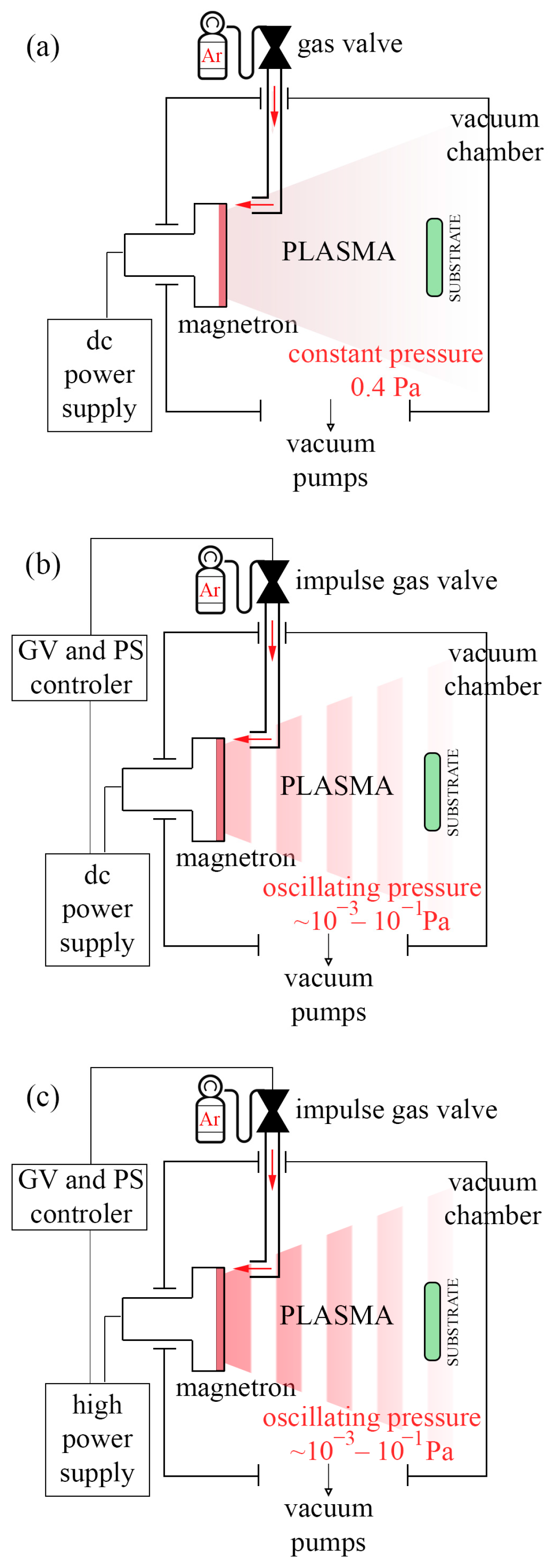
Figure 1. Diagrams of vacuum apparatus used in the experiment: (a) PMS, (b) GIMS, and (c) HiPGIMS.
Coatings 15 01367 g001
Figure 2. Voltage and current waveforms registered in the electric circuits of the magnetron cathode during the operation of PMS (a), GIMS (b), and HiPGIMS (c) processes.
Coatings 15 01367 g002
Figure 3. The OES spectra of plasma generated by various versions of MS (a), the trends of intensity of chosen spectral lines of: C I (b), C II (c), Ar I (d), and Ar II species (e).
Coatings 15 01367 g003
Figure 4. AFM images of the a-C layers’ surface with the S a roughness parameter calculated.
Coatings 15 01367 g004
Figure 5. Raman spectra of a-C layers deposited by PMS (a,d), GIMS (b,e), and HiPGIMS (c,f) collected during irradiation by 532 nm laser (left column) and 266 nm laser (right column).
Coatings 15 01367 g005
Figure 6. The sp3/sp2 ratio in a-C layers was calculated by Raman spectroscopy and the XPS method.
Coatings 15 01367 g006
Figure 7. XPS C1s (left column), O1s (middle column), and Ar2p/Si2p (right column) core levels of a-C layers synthesized by: PMS (a,d,g), GIMS (b,e,h), HiPGIMS (c,f,i).
Coatings 15 01367 g007
Figure 8. Optical properties of a-C layers deposited by various MS techniques: refractive index n, extinction coefficient k, absorption coefficient α, and Tauc plot with Eg bandgap determination.
Coatings 15 01367 g008
Table 1. Technological parameters of sputtering processes.
PMSGIMSHiPGIMS
tAr (ms) -44
T (Hz) -22
D (%) 100100.2
Jdmean (mA/cm2) 142374
Pdmean (W/cm2) 10186
pAr (Pa) 0.4 (steady)10−3–10−1 (oscillating)10−3–10−1 (oscillating)
tpulse (ms) -501
tproc (min) 10120120
Table 2. Spectral lines characteristics assigned to the spectra measured in the experiment.
Observed Wavelength (nm)SpeciesLower LevelUpper LevelIntensity (arb. u.)
PMSGIMSHiPGIMS
403.7C I2s22p3s2s22p5p430340in noise
405.1Ar II3s23p4(1D)4s3s23p4(1D)4p390301in noise
406.7C I2s22p3s2s22p5p625671778
410.2Ar II3s23p4(3P)4p3s23p4(3P)5s233515in noise
412.8Ar II3s23p4(1D)4s3s23p4(1D)4p760924in noise
415.5C I2s2p32s22p7p1597963in noise
418.3Ar I3s23p5(23/2)4s3s23p5(23/2)5p878401in noise
419.5Ar I3s23p5(23/2)4s3s23p5(23/2)5p27692153in noise
422.6C I2s2p32s22p(21/2)6f329475in noise
425.3Ar I3s23p5(21/2)4s3s23p5(21/2)5p19291569778
427.4C I2s22p3s2s22p5p19292192856
429.6Ar I3s23p5(23/2)4s3s23p5(23/2)5p817671in noise
432.9Ar II3s23p4(3P)4s3s23p4(3P)4p10319461401
434.4C I2s2p32s22p6p109226025145
436.6C II2s2p(3P°)3d2s2p(3P°)4f66410631131
437.7C II3s23p4(3P)4s3s23p4(3P)4p369671992
439.7Ar II3s23p4(3P)4p3s23p4(3P)5s2949061872
441.9Ar II3s23p4(3P)4d3s23p4(3P)4p4868671480
446.7C I2s2p32s22p(23/2)5f329223in noise
447.7C I2s2p32s22p(23/2)5f468458in noise
450.5Ar I3s23p5(21/2)4s3s23p5(23/2)5p604401in noise
454.1Ar II3s23p4(3P)4s3s23p4(3P)4p11491433682
457.3Ar II3s23p4(3P)4s3s23p4(3P)4p525924896
458.5Ar II3s23p4(1D)4s3s23p4(1D)4p118815121092
460.3Ar II3s23p4(1D)3d3s23p4(1D)4p185023271676
465.6Ar II3s23p4(3P)4s3s23p4(3P)4p126617651149
471.9Ar II3s23p4(3P)4s3s23p4(3P)4p120917041305
473.2C I2s2p32s22p5p73914902338
475.7Ar I3s23p5(23/2)4p3s23p5(23/2)8d233828941401
480.2C I2s2p32s22p5p113123494286
484.3C I2s22p3p2s22p(21/2)16d5869061519
487.5C I2s22p3s2s22p4p210330903001
493.1C I2s22p3s2s22p4p369536817
496.1Ar II3s23p4(3P)4s3s23p4(3P)4p9951024935
501.1C I2s22p3p2s22p(21/2)10d4687891052
505.4C I2s22p3p2s22p(23/2)7d4477321092
Table 3. Parameters of fitted G and D peaks of a-C layers Raman spectra.
G peakD peak
Position (cm−1)FWHM (cm−1)Intensity (arb. u.)Position (cm−1)FWHM (cm−1)Intensity (arb. u.)
266 nmPMS1572.8162.1288.01381.9342.953.7
GIMS1580.4154.9594.91383.1300.4194.7
HiPGIMS1598.3100.4220.51371.2303.250.6
532 nmPMS1538.5195.5347.21373.6273.7176.7
GIMS1539.4188.2488.01366.7296.9263.5
HiPGIMS1537.3162.21026.81366.4320.8481.1
Table 4. Chemical compositions of a-C layers synthesized by various MS techniques.
C
(sp2)
C
(sp3)
C
(C–O)
C
(C=O)
O-COHO=CSiO2Ar%C%O%Si%Ar
PMS63.7210.6814.194.343.660.312.74-0.3692.936.7100.36
GIMS62.1312.2214.443.544.510.622.03-0.5192.337.1600.51
HiPGIMS45.0917.7719.873.499.880.790.822.29-86.2211.492.290
Disclaimer/Publisher’s Note: The statements, opinions and data contained in all publications are solely those of the individual author(s) and contributor(s) and not of MDPI and/or the editor(s). MDPI and/or the editor(s) disclaim responsibility for any injury to people or property resulting from any ideas, methods, instructions or products referred to in the content.