Article

Structure, Composition and Optical Properties of Thin Films of Copper Sulphide and Bismuth Sulphide Deposited on Various Textiles by the SILAR Method

by
Vėja Sruogaitė
and
Valentina Krylova
*
Faculty of Chemical Technology, Kaunas University of Technology, Radvilenu Str. 19, LT-50254 Kaunas, Lithuania
*
Author to whom correspondence should be addressed.
Coatings 2025, 15(11), 1266; https://doi.org/10.3390/coatings15111266 (registering DOI)
Submission received: 23 September 2025 / Revised: 24 October 2025 / Accepted: 28 October 2025 / Published: 2 November 2025
(This article belongs to the Special Issue Advances in Coated Fabrics and Textiles)

Abstract

The synthesis of thin films in multilayer structures on different textiles is of interest due to their potential use in flexible solar absorber coatings and thin-film solar cells. The aim of the study was to deposit bismuth(III) sulphide and copper(II) sulphide thin films on various textiles at the same time. This was achieved using the sustainable and cost-effective successive ionic layer adsorption and reaction (SILAR) method. The study examined how the elemental distribution, phase composition, crystallinity, surface morphology, and optical features of the resulting films are determined by the intrinsic structure and material makeup of structural textiles. The analysis used data from scanning electron microscopy (SEM), energy dispersive X-ray (EDX) spectroscopy and X-ray diffraction (XRD), as well as ultraviolet-visible (UV-Vis) diffuse reflectance spectroscopy. Depending on the textiles used, the formed films were polycrystalline and rich in copper. According to the findings, the normalised atomic percentages were as follows: Cu, 57.66–68.75%; Bi, 1.19–5.26%; S, 30.06–38.63%. The direct transition optical energy gap values varied from 1.3 to 2.88 eV, while the indirect varied from 0.9 to 2.25 eV, and the refractive index from 1.3 to 1.8. These properties were influenced by the composition of the textiles and the films themselves. These properties directly impact the films’ applications.

1. Introduction

As concern for sustainability rises, the adoption of renewable energy sources accelerates. In 2024, more than 40% of global electricity was generated using alternative sources, this increase was led by solar power [1]. Most photovoltaic (PV) solar systems use crystalline silicon solar cells (SCs), which have drawbacks related to the cost inefficient, arduous process of silicon production, and limited flexibility of solar cells, as they are stiff and fragile. While the study of perovskite solar cells has been comprehensive and the appeal of their simple design is apparent, they are characterised by instability as semiconductors for charge transfer. Moreover, they exhibit inflexibility and are unusable in instances where a pliable and slight PV generator is required. The potential of creating flexible textile-based photovoltaic systems arose from using textiles in electronic devices, which led to them exhibiting exceptional performances. Finding suitable textiles and semiconductors is a key element in alternative PV system production.
Electrically conductive textile fabrics are made using conductive yarns. These yarns can be produced using chemical coatings or metallisation (with copper, silver or nickel nanoparticles). In metallisation, Ag and Cu show the highest value of electrical conductivity (around 642 S/m) [2]. The full silver- or copper-plated yarns, mostly using polyamide (PA), can be twisted, knitted, embroidered, woven and spun. Fabrics with surface metallisation are conductive and have an electrical resistance of less than 1 Ω/sq [2]. Their high electrical and thermal conductivity makes them suitable for use as current conductors for sensors and other applications.
Several materials show potential and are presently used for industrial implementation, for example: polyvinylchloride (PVC) coated polyester (PES) fabrics, polytetrafluoroethylene (PTFE) coated glass fibre (GF), etc. Polycotton is a blend of synthetic polyester and spandex (S) fibres intertwined with natural cotton (C) fibres to create a fabric that combines the best qualities of all three materials [3]. This combination produces a fabric that is stretchy, durable and easy to care for, making it ideal for a wide range of items. Characteristics like resilience, conductivity and energy efficiency of common fabrics can be enhanced by the deposition of semiconductor thin films.
Since being used in optoelectronic and advanced electronic devices, nanocrystalline semiconductors gained interest, due to their distinctive optical and structural properties. One of these semiconductors is a metal sulphide. Due to their unique properties, metal sulphides are gaining attention for expanding their application in electronics, optics, electrochemical detection, photocatalysis, biomedicine, energy storage and conversion [4,5,6,7].
As indicated by studies, copper sulphides are p-type semiconductors, used in optoelectronics [8], in lithium rechargeable batteries as cathode materials [9], for heterojunction diodes [10], and as gas sensors [11] and electrode materials for supercapacitors [12]. Nanocrystalline copper sulphide has at least five stable crystallographic phases at room temperature, which vary in their Cu:S molar ratio, from copper-rich chalcocite (orthorhombic Cu2S) to copper-deficient covellite (hexagonal CuS) phase. Chalcocite is the most widely studied of these compositions. The covellite phase can be used as a superconductive material due to holes present in its valence band, which are aligned with the 3p orbitals of sulphur [13]. Due to having a band gap of 1.21 eV, which can be tuned by changing the morphology, copper sulphides are compatible with properties required for their usage in solar cells [14] and photosensors [15]. Because of the efficient absorption in the near-infrared region, which can be altered by changing stoichiometries, copper sulphides show potential to be used in biomedical industries [16]. Furthermore, copper sulphides display metal-like electrical conductivity [17], increased conductivity at high temperatures [18], excellent electrochemical properties [9,19,20], and properties that align with excellent solar radiation absorption [21]. Copper sulphides are prone to form nanostructures with various morphologies, for example nanotubes, nanowires, nanospheres, nanoplates, nanorods, nanoflowers, nanoribbons [22].
Bismuth-based compounds are attractive due to bismuth’s versatility; it is found in ores such as bismuthinite (bismuth(III) sulphide) and bismite (bismuth(III) oxide) [23]. As it is a harmless element, bismuth is considered a ‘green metal’. Bi2S3 is used in several industries for thermoelectric cooling technologies [24], photovoltaic converters, photo-catalysts [19], and hydrogen storage [25], as a thermoelectric gas sensor [26,27], for optical detection for IR and UV light [28,29], photoelectrochemical solar cells, and electronic and optoelectronic devices [30]. It is a non-toxic n-type crystalline semiconductor, characterised by a low direct energy band gap (1.3–1.7 eV), which is in the optimal range of the solar spectrum. Furthermore, it displays exemplary properties, such as high ionic conductivity, adequate conversion efficiency of incident photons to electrons (~5%) [24], and a high absorption coefficient of 104–105 cm−1, which are in line with solar energy conversion devices [31]. Bismuth(III) sulphide exhibits an orthorhombic, lamellar structure held together by weak Bi–S bonds and is prone to form several nanostructures, including belts, spheres, stars, snowflakes, ribbons, flowers, rods, tubes, and wires [32,33,34,35,36]. Bi2S3 thin films have the potential to be used for memristors [37], cancer diagnostics [38,39], and lithium-ion batteries’ anode material [40].
Recently, a new class of bismuth-based chalcogenide materials has gained considerable attention due to its interesting optoelectronic properties and performance. This class comprises the ternary compounds I3-V-VI3, one of which is Cu3BiS3, also known as bismuth sulfosalt of copper or wittichenite. This material is non-toxic and abundant in the Earth’s crust. It is a stable phase with a low melting point of approximately 527 °C [41], demonstrating the potential for grain growth at low temperatures. It exhibits remarkable optoelectronic properties, including a strong absorption coefficient (>105 cm−1) in the visible spectrum, p-type conductivity and an energy bandgap of 1.10–1.86 eV [42], which falls within the optimum range for various applications. Consequently, bismuth-based chalcogenides have emerged as promising light absorbers due to their high optical absorption coefficient.
Copper bismuth sulphides show characteristics that align with the requirements for photovoltaic application, such as fitting band gap and high optical absorption abilities in the visible spectrum [43]. Furthermore, studies show that there is a growing demand for energy storage devices, and copper bismuth sulphides show promise for use in supercapacitors [44] and as photo absorbers and photocatalysts [45].
The physical methods of depositing bismuth and copper sulphides are well studied and include the ultrasonic method [46], thermal evaporation [47], microwave irradiation [35], spray pyrolysis [48], and pulser laser deposition [49]. However, these methods are costly and demanding, involving ultrahigh vacuums and high temperatures, and requiring complex equipment and high costs.
As an alternative, successive ionic layer adsorption and reaction (SILAR) [50,51] and chemical bath deposition (CBD) [52] provide a straightforward process. However, there are disadvantages to CBD film formation. The main problems with CBD are a lack of fundamental understanding of its chemistry, which hinders process optimisation, and poor control over film growth, which leads to inconsistent film properties and morphology. Specific issues include inefficient use of reactants, significant waste generation and limited control over film thickness due to supersaturation. The SILAR method is advantageous since the precursors are placed separately. One SILAR cycle involves immersing the substrate in a bath containing a cationic or an anionic precursor solution for a set period of time. Afterwards, the substrate is rinsed and placed in another bath for the same or a different amount of time. Each precursor solution may have a different required temperature. The deposition rate and film thickness are controlled by the immersion duration and number of cycles. In this study, the SILAR method was chosen to form copper bismuth sulphide thin films.
Various precursors are used to prepare thin metal chalcogenide films [21,41,50,51,52]. The binary solvent approach, for example, can be used to produce soluble precursors for a variety of metal chalcogenide semiconductors, such as Cu2X, Bi2X3 and SnX, where X = S, Se or Te, at room temperature and pressure. These chalcogenide–metallate precursors could potentially be used to coat fabrics in the future [53].
We have previously reported on the preparation of thin films of bismuth sulphide with respect to their application as photovoltaic components [50]. The structure, composition and thermal stability offered by chemical methods deposited on copper bismuth sulphide thin films in single and multilayer structures are of interest due to their potential applications in solar control and absorber coatings. Their potential use in thin-film solar cells has also been explored. This paper reports on XRD and SEM/EDS analyses of the films and their resulting effects on optical reflectance and absorbance, as well as providing information about their structures and surface resistivity. Such properties directly impact their applications.

2. Materials and Methods

2.1. Materials

Four samples of textiles with different compositions were selected for the deposition of copper bismuth sulphide thin films. Table 1 shows the composition and characteristics of each textile. For the investigations, the textiles were cut into 2 cm × 7 cm samples, with three identical samples taken from each textile.
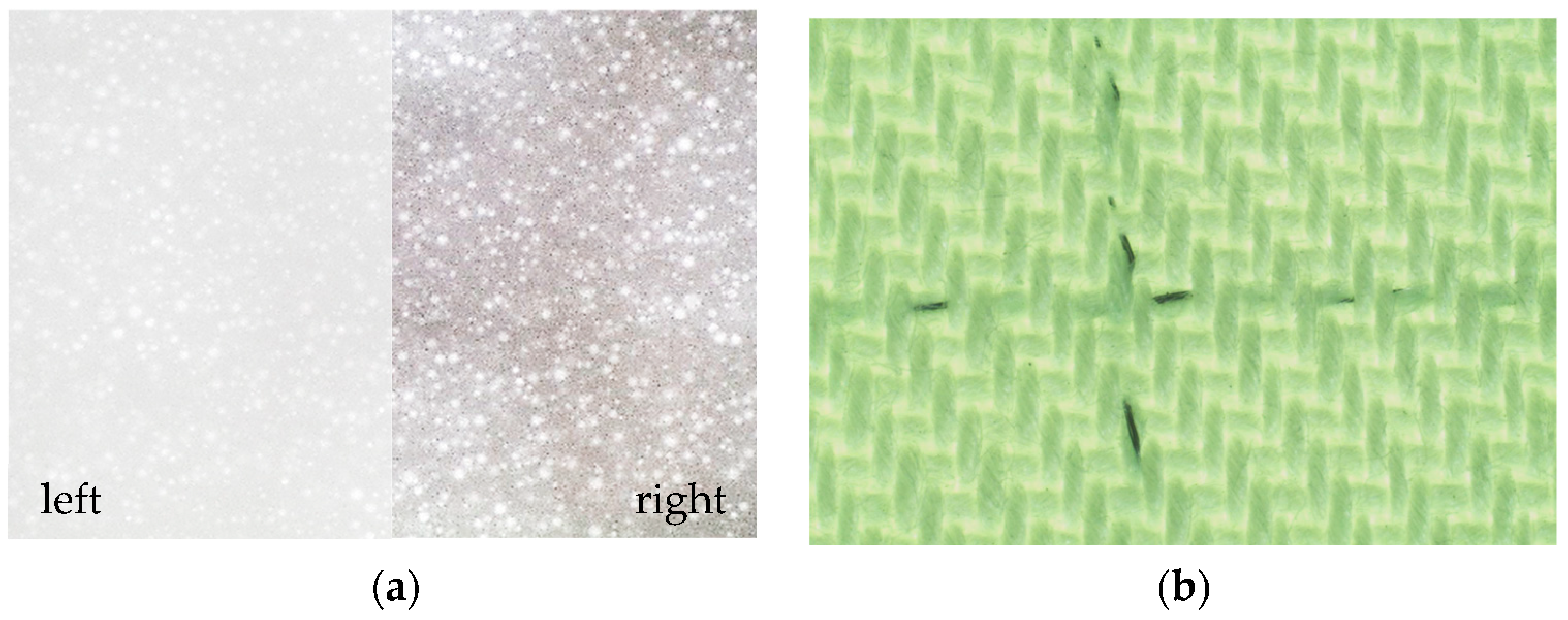
Figure 1 shows textural views of PA/Ag and PA/Cu textiles taken with a stereo microscope. PA/Ag is a knitted fabric with a metallic, silver-grey colour (Figure 1a), while PA/Cu is a woven fabric with a red-brown copper colour (Figure 1b).
Textural views of PET/PVC and C/PES/S textiles taken with an optical microscope are shown in Figure 2. The PET/PVC textile has a smooth, white surface with evenly distributed spherical filler particles (see Figure 2a on the left), which become more visible when the brightness and contrast of the image are increased (see Figure 2a on the right). The C/PES/S textile is a woven cotton fabric in a green colour with dark spandex thread (see Figure 2b).
To increase their adhesive properties, the PET/PVC samples were roughened and thermo-oxidatively acid-treated in a solution mixed with 7.2 M H2SO4, 6.6 M H3PO4 and 0.36 M CrO3 at 68 ± 1 °C before deposition, according to the procedure described in our previous work [50]. The reagents used to prepare the solutions are listed in Table 2.

2.2. Deposition of the Cu–Bi–S Thin Films

The bismuth sulphide films were deposited using the SILAR method. Bismuth(III) nitrate provides bismuth ions (Bi3+), copper(II) sulphate provides copper ions (Cu2+) and sodium thiosulphate provides sulphide ions (S2−). The solubility product of Bi2S3 is Ksp = 1 × 10−97 (mol/L)5 [54], and the molar solubility is approximately 1.55 × 10⁻²⁰ mol/L. The solubility product of CuS is Ksp = 6.0 × 10−37 (mol/L)2 [54], and the molar solubility is S = 7.75 × 10⁻¹⁹ mol/L. In order to deposit mixed Cu–Bi sulphide thin films, the less soluble Bi2S3 must be deposited first. Only then can the CuS film be deposited. Otherwise, some of the deposited CuS will either turn into Bi2S3 or dissolve in an acidic Bi(NO3)3 solution due to hydrolysis. Water is likely involved in the reactions as a solvent to facilitate the formation of sulphides. The basic equations of the reactions can be described as follows:
2 Bi ( NO 3 ) 3 ( aq ) + 3 Na 2 S 2 O 3 ( aq ) + 3 H 2 O ( l ) Bi 2 S 3 ( s ) + 3 H 2 S O 4 ( aq ) + 6 NaNO 3 ( aq ) ,
CuSO 4 ( aq ) + Na 2 S 2 O 3 ( aq ) + H 2 O ( l )     CuS ( s ) + Na 2 S O 4 ( aq ) + H 2 S O 4 ( aq ) .
The process parameters for depositing these thin films were fine-tuned through repeated experimentation. This included adjusting the concentration of the reagents, the temperature of the solutions, and the exposure time for one cycle and number of cycles until the desired quality of thin film was achieved. The deposition conditions for the Cu-Bi sulphide thin films are shown in Table 3.
A list of sample codes and their descriptions is provided in Table 4.

2.3. Characterisation Methods

A Nikon SMZ445 stereo microscope (Nikon Instruments Inc., Amstelveen, The Netherlands), equipped with zoom magnification ranging from 0.8× to 3.5×, was used to capture textural views. The surface of the textile was imaged using an Olympus CX31 optical microscope (Olympus Corporation, Tokyo, Japan) with 100× magnification. Images of the optical microscope were captured using an Olympus C-5050 digital camera with a resolution of 2560 × 1920 pixels.
The resistance of the conductive textile fabrics was measured using a direct current numerical measuring device MS8205F (Mastech, Taipei, Taiwan, China) with custom-built electrodes. These were manufactured using two nickel-plated copper plates. These plates were fixed 1 cm apart and the material was placed between them.
XRD analysis was performed on a Bruker Advance D8 diffractometer (Bruker AXS, Karlsruhe, Germany) with a tube voltage of 40 kV and a tube emission current of 40 mA. A 0.02 mm Ni filter was used to filter the X-ray beam, in order to select CuKα (λ = 0.15406 nm) radiation. A fast-counting detector, the Bruker LynxEye, which is based on silicon strip technology, was used to record diffraction patterns in a Bragg–Brentano geometry. The specimens of the samples were scanned over the range of 2θ = 3–70°. The scan rate was 0.02°min−1. The coupled two theta/theta scan type was used. Determination of the phase composition of the formed films was done using Crystallographica Search-Match v. 2.1 and ConvX v. 1.0 software.
Scanning electron microscopy (SEM) measurements were performed using a Hitachi S-3400N (Chiyoda, Tokyo, Japan) microscope equipped with a Bruker Quad 5040 energy dispersive X-ray spectroscopy (EDX) system. The samples were mounted using carbon tape. Both the SEM and EDX analyses were performed using an accelerating voltage of 10 kV. Images were captured using a secondary electron detector in standard high vacuum mode. Prior to recording the spectra, the EDX detector was cooled to −20 °C and its energy scale was calibrated using the Mo standard. The elements detected with EDX were quantified using the standard-less ZAF method.
UV-Vis diffuse reflectance spectra were recorded using a Lambda 35 UV-Vis spectrophotometer (Waltham, MA, USA). Barium sulphate was used as a white standard. The Kubelka–Munk method was employed to calculate the optical energy gap (Eop), using the following equations [55,56]:
F R = 1 R 2 2 · R ,
h v F ~ ( h v E o p ) n .
The Kubelka–Munk function (F), reflectance (R), photon energy () and band gap (Eop) are all key elements in this equation. n is a constant called the power factor of the transition mode. n takes values 1/2, 1/3, 2 and 2/3 for indirect allowed, indirect forbidden, direct allowed and direct forbidden transitions, respectively.
The difference in the refractive index of the constituent materials causes significant light scattering in organic–inorganic composites [57]. The refractive indices (n) were determined from the reflectance (R) data using the following formula [58,59]:
n = R + 1 ± 2 R R 1

3. Results and Discussion

The formation of a new phase on the surface of the textile samples under investigation confirms the dark black colour of the composites obtained. The adhesion of the deposited Cu–Bi–S films was tested by subjecting them to a steady stream of distilled water [60]. It has been demonstrated by the tests that thin films deposited on the textile substrates have adhered well.
Table 1 shows the measured surface resistance of the conductive textile fabrics only. Silver has a higher electrical conductivity than copper due to its greater concentration of free electrons and more efficient electronic structure, which allows electricity to flow more freely through it. However, the measured surface resistance of the PA/Ag textile sample was higher than that of the PA/Cu sample: 4.4 Ω/sq and 2.4 Ω/sq, respectively. This can be explained by the thickness of the PA fibres, since conventional polyamide fibre is an insulating material. The PA/Ag textile is almost twice as thick as the PA/Cu textile and has a basis weight that is 1.5 times lower (see Table 1). To evaluate the effect of the deposited Cu–Bi sulphide films on the electrical conductivity of these textile samples, their surface resistivity was measured. For composite S2 (PA/Ag textile substrate), the resistivity was 30 Ω/sq, whereas for sample S3 (PA/Cu textile substrate), it was 52 Ω/sq. The lower resistance of composite S2 suggests that thin films with a higher conductive phase ratio to the total film volume were formed.

3.1. XRD Characterisation

XRD was used to carry out the phase composition characterisation of the obtained Cu–Bi sulphide thin films on the surface of different structural textiles. We used a combination of data from the literature, our own data on bulk copper and bismuth sulphides precipitated under the same conditions as thin films, and JCPDS reference patterns to perform a detailed analysis of the XRD data.
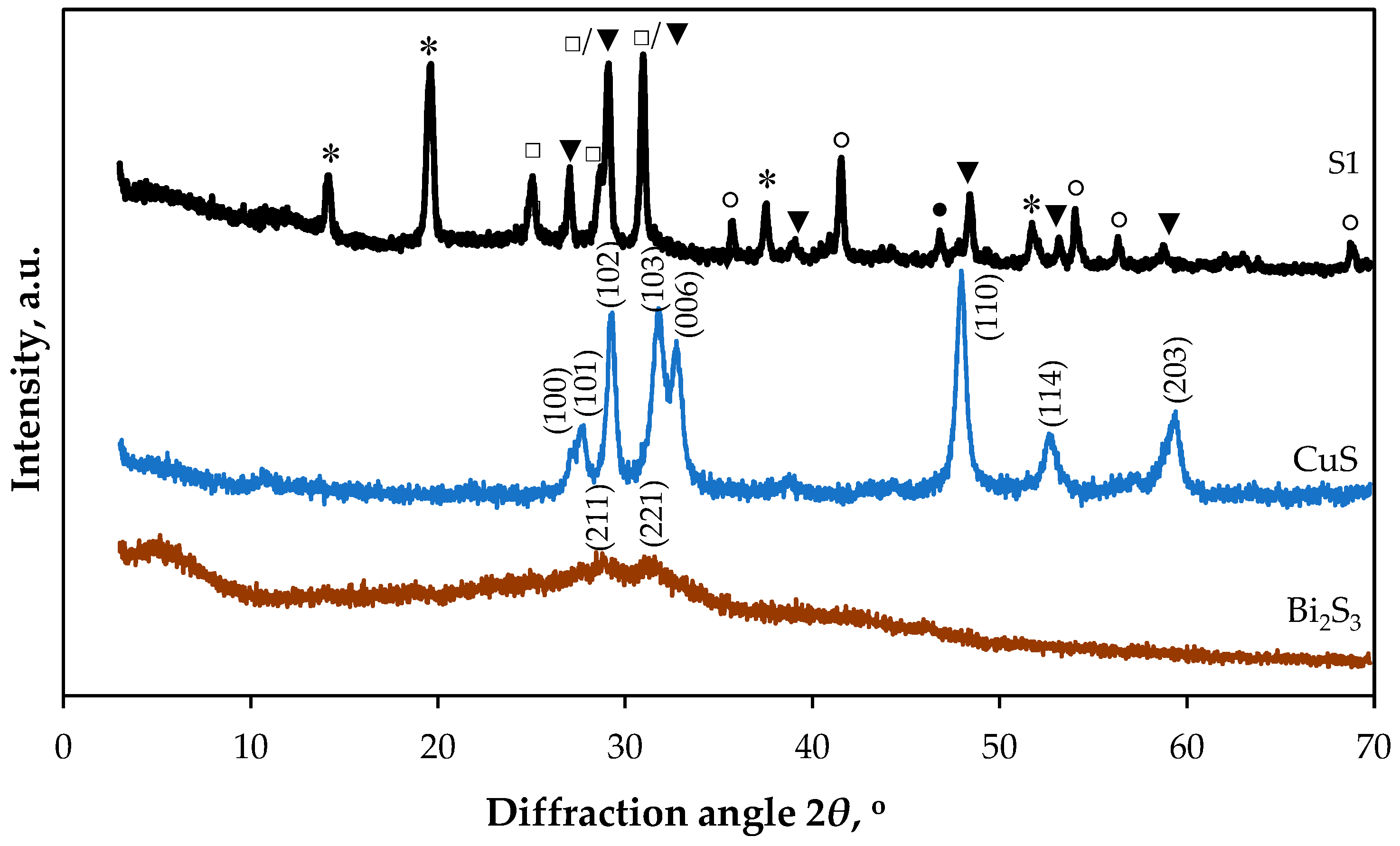
Figure 3 shows the diffractogram patterns of the S1 sample, as well as the copper and bismuth sulphide sediments. As previously reported [61], chemically deposited Bi2S3 films are often amorphous or polycrystalline in their as-deposited state. The presence of XRD peaks at 2θ = 28.45° and 31.57° in the bismuth sulphide sediment indicates that it is polycrystalline (see Figure 3). These peaks are attributed to the orthorhombic phase of Bi2S3, with the following crystallographic planes: (211) and (221) (JCPDS: 17-320).
All the primary diffraction peaks in the XRD curve of the copper sulphide sediment (Figure 3) are in good agreement with the standard data for the hexagonal structure of covellite (CuS, JCPDS: 78-0876). The 2θ Bragg angles of 27.27°, 27.78°, 29.31°, 31.78°, 32.74°, 47.95°, 52.62° and 59.39° correspond to the (100), (101), (102), (103), (006), (110), (114) and (203) directions, respectively.
PET/PVC is a PVC-coated, woven PET fabric consisting of multiple components. In this composite, the woven PET fabric is stabilised and protected by the main and top PVC coatings. The main PVC coating comprises the PVC polymer itself, a softener, calcium carbonate (CaCO3), a thermo-stabiliser, and a UV absorber. The top coating contains titanium dioxide (TiO2), which provides UV stability. The characteristic peak at 2θ = 46.85° corresponds to the (018) crystal plane of rhombohedral calcite (CaCO3, JCPDS: 05-0586). Similarly, five characteristic peaks at 2θ = 35.74°, 41.55°, 54.03°, 56.32° and 68.78° correspond to the (101), (200), (211), (220) and (301) crystal planes of the tetragonal rutile phase of titanium dioxide (TiO2, JCPDS: 04-006-1890) (see Figure 3, composite S1).
Many of these peaks correspond well with the XRD data obtained for bulk Bi2S3 and CuS. However, the specific 2θ values and their corresponding intensities slightly differ depending on the crystal quality and form (bulk or thin film). Some CuS and Bi2S3 peaks overlap (see Figure 3, sample S1). Peaks at 2θ = 14.13°, 19.62°, 37.55° and 51.73° are attributed to the orthorhombic phase of Cu3BiS3 (wittichenite) with the following crystallographic planes: (310), (111), (311) and (340) (JCPDS: 43-1479).
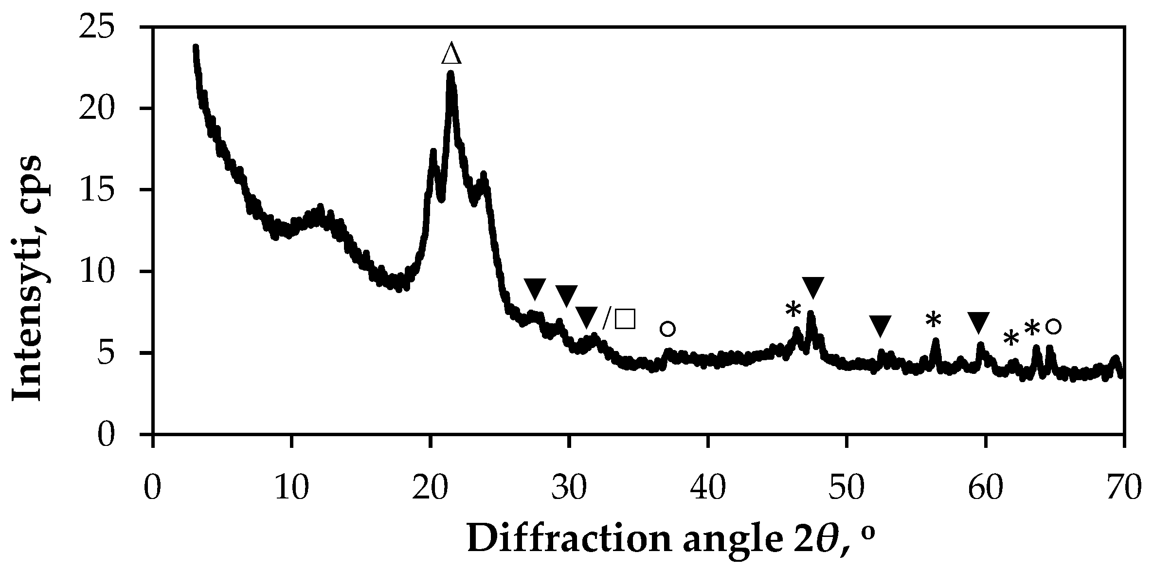
The XRD pattern of the Cu–Bi sulphide films deposited on a textile consisting of a PA fibre fabric with an Ag coating is shown in Figure 4. The XRD peaks are located at 2θ = 21.50°, 27.17°, 29.23°, 31.53°, 37.18°, 46.30°, 47.34°, 52.48°, 56.36°, 59.60°, 61.96°, 63.60° and 64.58°. Specifically, the peak at 2θ = 21.50° is attributed to the (001) crystal lattice plane of the γ-phase of PA6 in JCPDS: 12-923. Two additional peaks of different intensity were also registered at 2θ = 37.18° and 64.58°, corresponding to the face-centred cubic silver crystal lattice planes (111) and (220) (JCPDS: 04-0783), respectively. The other peaks of different intensity at 2θ = 27.17°, 29.23°, 47.34°, 52.48° and 59.60° are attributed to the hexagonal structure of covellite (CuS, JCPDS: 78-0876), with the following crystallographic planes: (100), (102), (110), (114) and (203). The peak at 31.53° can be attributed to CuS (crystallographic plane (103)) in relation to Bi2S3 (crystallographic plane (221)) (JCPDS: 17-320). The other peaks at 2θ = 46.30°, 56.36°, 61.96° and 63.60° are indexed to the orthorhombic phase of Cu3BiS3 (JCPDS: 43-1479) with the following crystallographic planes: (131), (241), (322) and (340).
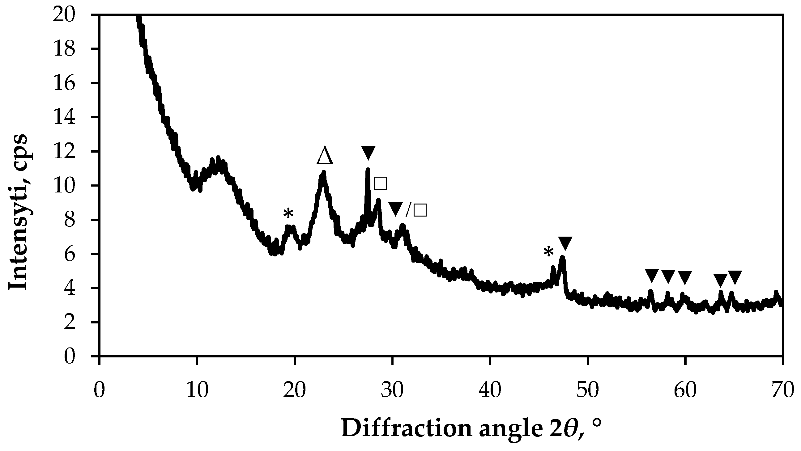
The XRD pattern of the Cu–Bi sulphide films deposited on a textile consisting of a PA fibre fabric with an Cu coating is shown in Figure 5. The peak at 2θ = 22.68°, assigned to the crystal lattice plane 002/202 of the α-crystalline form of PA6 (JCPDS: 022-0700). Peaks at 2θ = 19.72° and 46.30° are attributed to the orthorhombic phase of Cu3BiS3 (wittichenite) with the following crystallographic plane (340) and (131) (JCPDS: 43-1479). The XRD peak at 2θ = 28.52° are attributed to the orthorhombic phase of Bi2S3, with the following crystallographic plane (211) (JCPDS: 17-320). The peaks located at 2θ = 27.45°, 47.30°, 56.38°, 59.43°, 61.92°, 63.62° and 64.98° are attributed to the hexagonal structure of covellite (CuS, JCPDS: 78-0876), with the following crystallographic planes: (100), (102), (110), (114) and (203). The peak at 31.49° can be attributed to CuS (crystallographic plane (103)) in relation to Bi2S3 (crystallographic plane (221)) (JCPDS: 17-320).
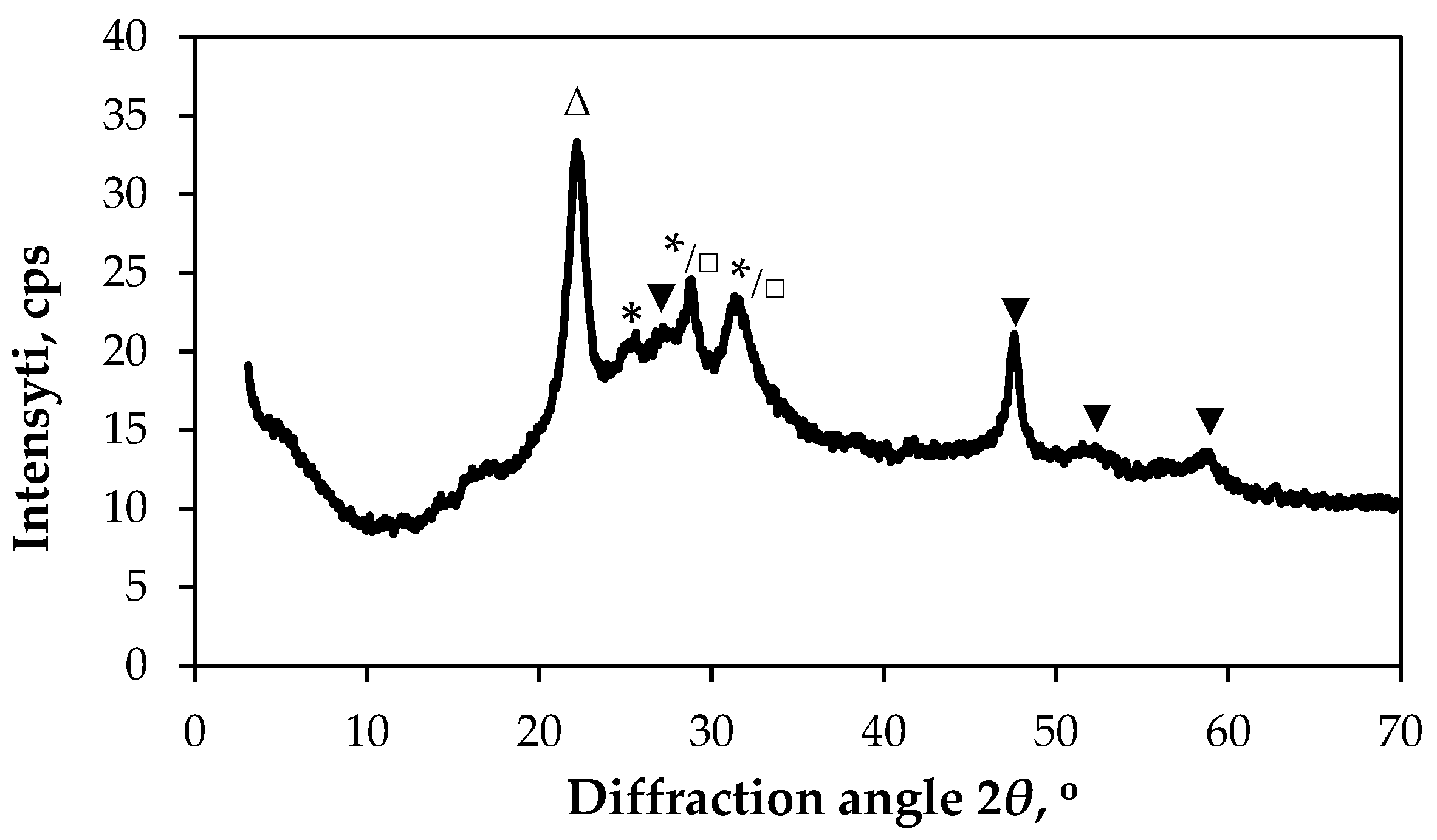
The diffraction patterns of the S4 samples (Figure 6) exhibited the peaks at around 2θ = 22.09°, 25.39°, 27.45°, 28.84°, 31.29°, 47.54°, 51.46° and 58.66°. The peak at 2θ = 22.09°, corresponding to the crystal lattice planes (220) of cellulose I, which is found within the cotton fibres (JCPDS: 03-0226). The peak at 25.39° attributed to orthorhombic Cu3BiS3 (JCPDS: 43-1479). The peaks at 2θ = 27.45°, 47.54°, 51.46° and 58.66° are indexed to the hexagonal structure of covellite (CuS, JCPDS: 78-0876), with the following crystallographic planes: (100), (110), (108) and (203/116). The peaks at 28.84° and 31.29° can be attributed to Cu3BiS3 (crystallographic planes: (220) and (131)) as well to Bi2S3 with (211) and (221) directions (JCPDS: 17-320).
The XRD data obtained are consistent with the EDX results, which indicates that the deposited thin films are copper-rich. Therefore, the dominant phases in the deposited multiphase thin films are CuS and Cu3BiS3.

3.2. SEM/EDX Characterisation

SEM-EDX spectroscopy was evaluated for the analysis of the surface elemental composition of a material, as well as its morphology.
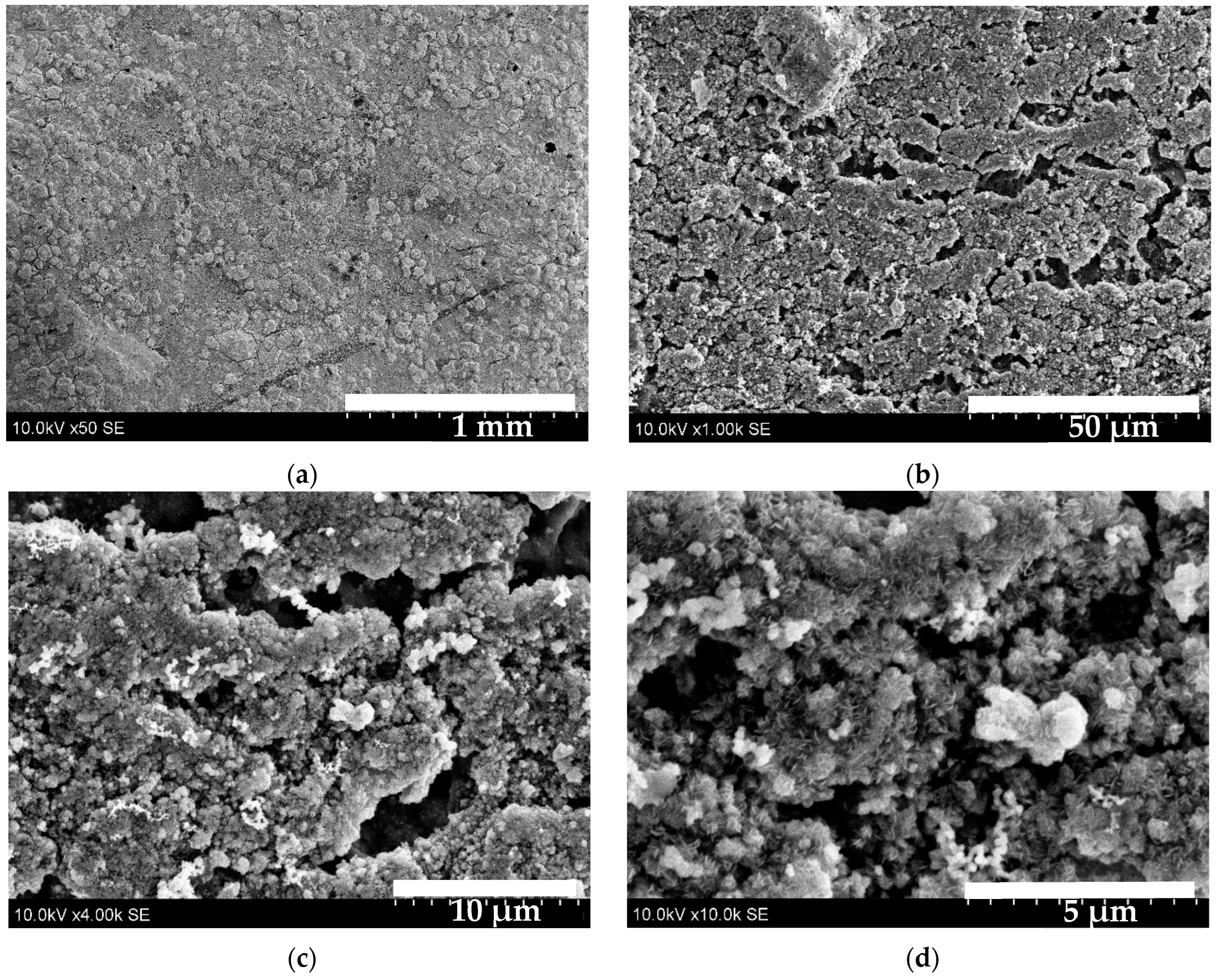
Figure 7 shows SEM images of the S1 sample. Image (a) shows a textured crystalline surface covered with rounded granular features. Cu–Bi–S granules are relatively uniform in size and densely packed forming a continuous layer. Upon higher magnification (image (b)) the surface exhibits a porous structure with irregularly shaped voids of varying sizes. Solid areas consist of small, agglomerated particles. Pores are not evenly distributed—some areas are densely packed with pores, while others are more compact. At 4000× magnification (image (c)) nanostructures become visible. The particles are not perfectly spherical; many appear angular or fused, and the exact shape of nanocrystals is unidentifiable. Image (d) shows an agglomeration of a nanoflake–shaped nanocrystalline structure.
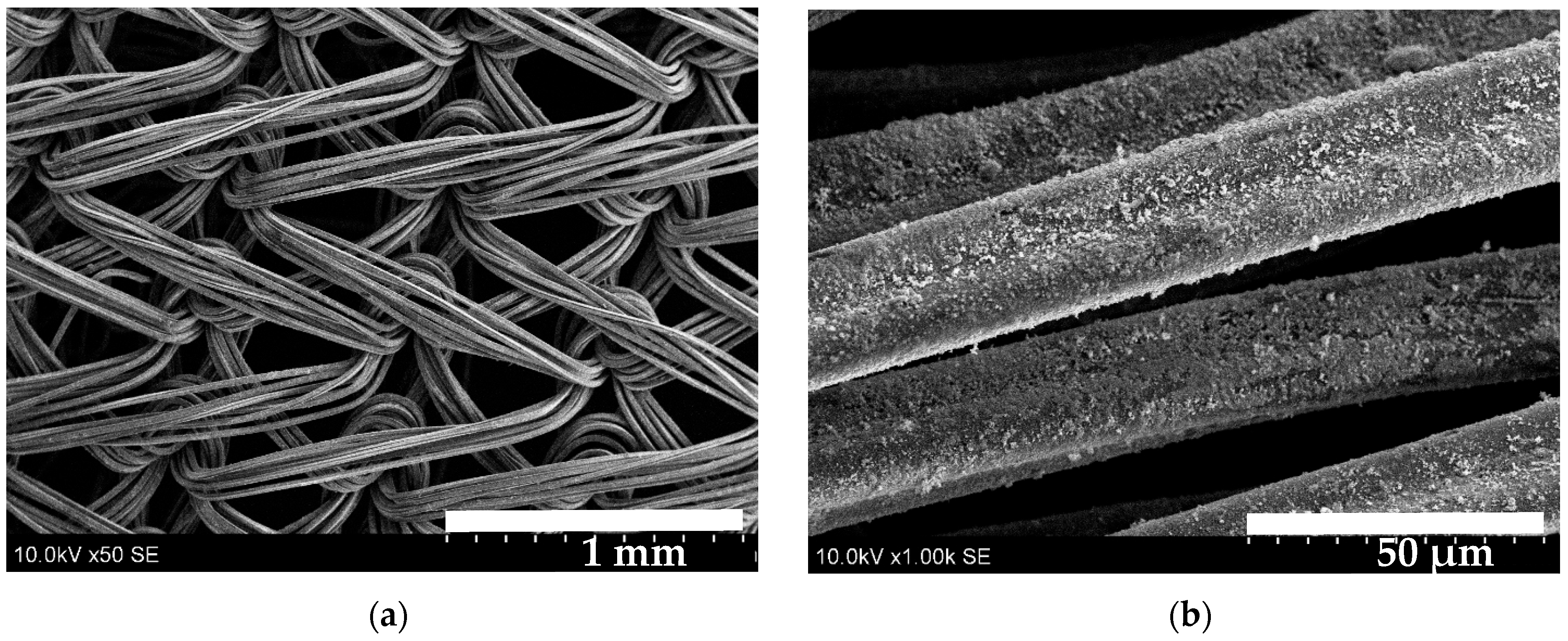
Figure 8 shows SEM images of the S2 sample. At 50× magnification (image (a)), the knitted texture of the fabric appears evenly coated, which is further confirmed at the higher magnification (image (b)). The fibre is covered by a homogenous layer; no pores or cracks are visible. Image (c) reveals that, although the strand is evenly coated, certain localized regions contain larger nanocrystals of varying shapes and sizes. Higher magnification (image (d)) shows nanoball-shaped nanocrystals that vary in size (0.45~1.36 µm) and are interconnected to form larger clusters.
Figure 9 shows SEM images of the S3 sample. At low magnification (image (a)), the woven texture of the fabric appears homogeneously coated. Higher magnification (image (b)) confirms that the strand is evenly coated, no pores or cracks are visible. Image (c) shows that the surface of the sample is roughly textured, nanocrystals are interconnected in a continuous nanocrystalline layer. These nanocrystals vary in both size and shape. At 10,000× magnification (image (d)) shows that nanoball-shaped crystals formed a homogenous layers and are clustered together.
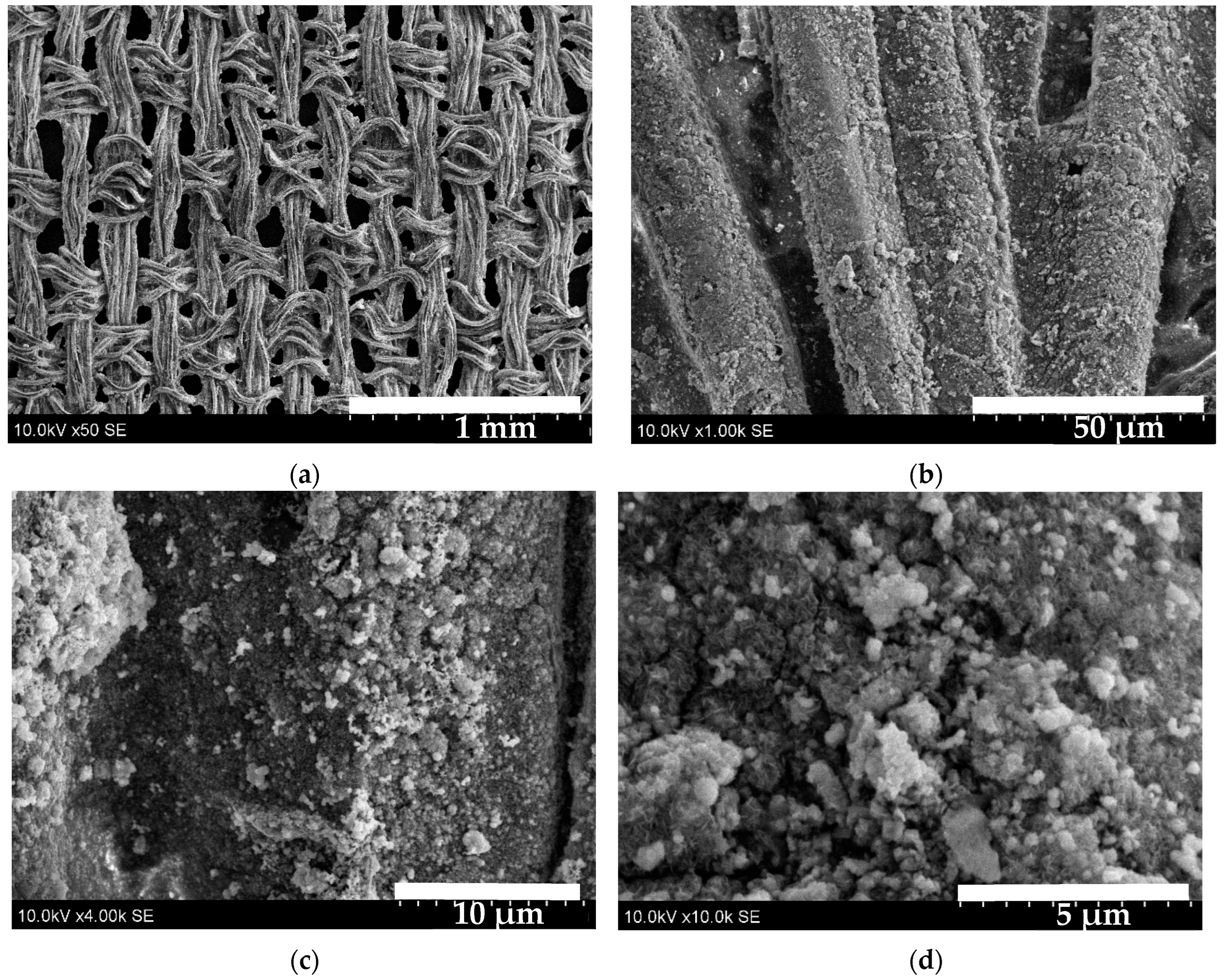
Figure 10 shows SEM images of the sample S4. These images show the complex, woven structure of the cotton fabric, with the threads and fibres clearly visible. Due to their small thickness and excellent adhesion to the fibre surface, the thin film particles on the fibre are practically invisible (image (a)). However, at higher magnification (image (b)), it can be seen that each fibre is covered in Cu–Bi sulphide particles of various sizes. While the coating may appear uneven, image (c) shows that there are no uncoated areas. Image (d) reveals individual crystallites about 100 nm of a distinctive shape that are closely spaced on the surface, as well as clusters of various sizes and shapes.
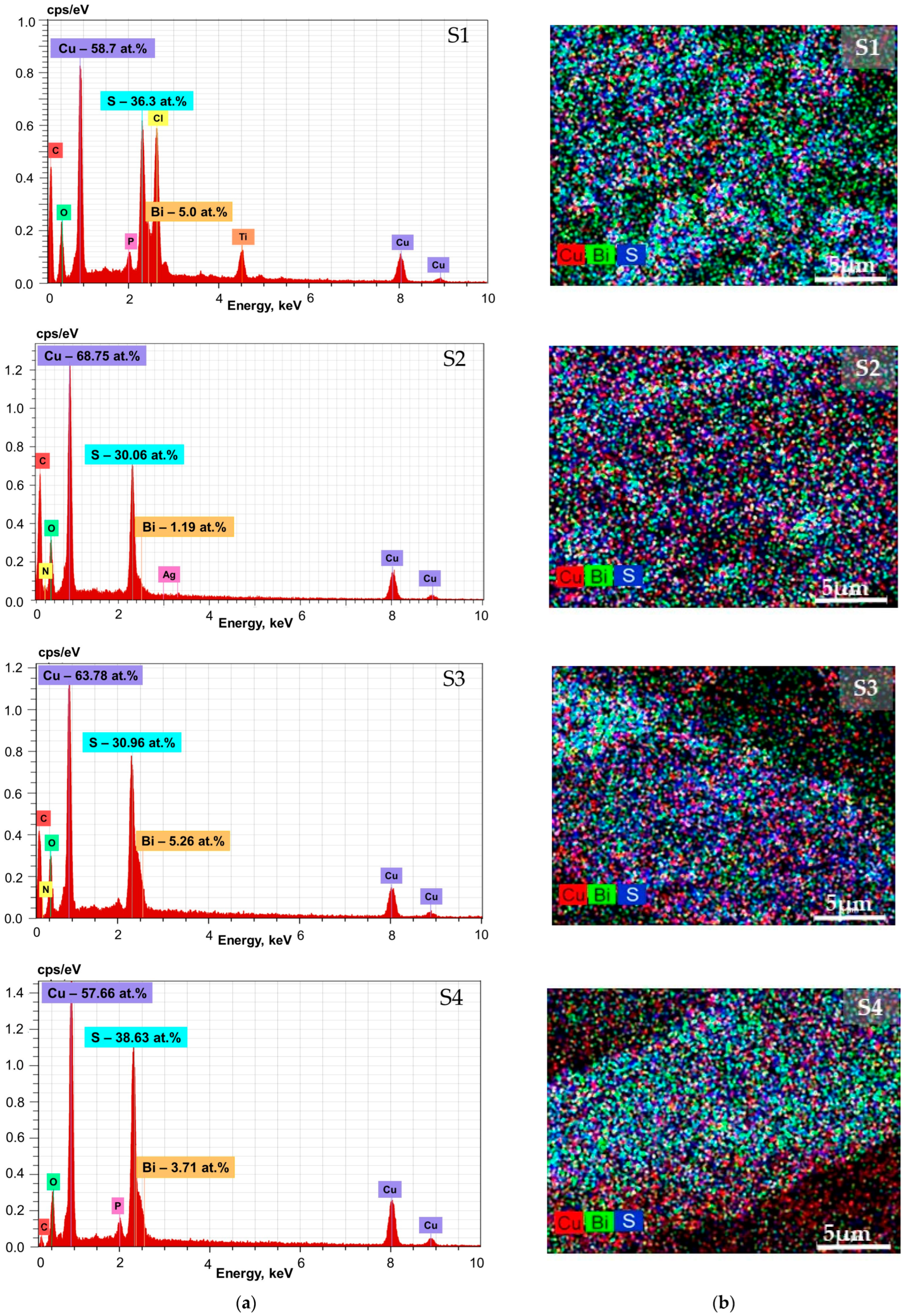
Reactions of bismuth and copper ions with thiosulphate ions occurred on the textile’s surfaces, combined with nucleation and growth of Cu–Bi sulphide particles, and enabled the development of particles immobilized on the surface, which are visible in SEM micrographs. EDX analysis confirmed the presence of Cu, Bi and S particles on the textile surface, as shown in Figure 11b.
Based on chemical elemental maps (Figure 11b) of the S1 and S4 samples, copper and sulphur are evenly spread out, while some localised areas contain more bismuth, which can be attributed to the formation of larger nanocrystalline structures. S2 and S3 elemental maps suggest a more even distribution of bismuth, copper and sulphur, which attributes to a more homogeneous composite surface.

3.3. UV-Vis Analysis

UV-Vis diffuse reflectance spectroscopy was used to characterise the optical properties of the obtained composites. This technique indirectly measures the material’s electronic structure and provides information about the electronic transitions of the different orbitals of a solid through the absorption spectra [55]. It has been reported that UV-Vis DR spectroscopy is the most effective method for evaluating the optical properties of textile fibres [62].
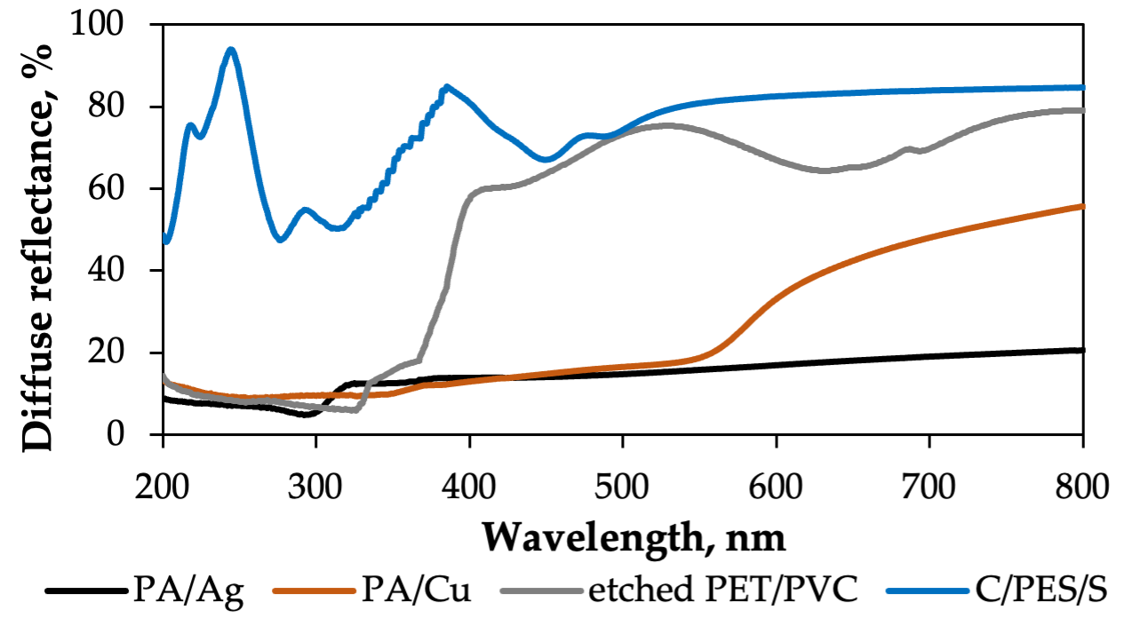
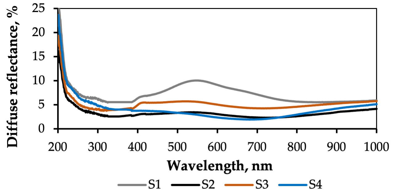
Figure 12 shows the reflectance values in the UV-Vis region of the textiles under investigation. For the etched PET/PVC textile sample, the spectrum shows 15–17% reflectance in the 200–330 nm range, increasing rapidly to 60% in the 330–400 nm range. The highest reflectance value is reached at 540 and 800 nm, with dips in reflectance at 440 and 640 nm. Figure 13 shows that the S1 composite has a consistent reflectance of 6% throughout the 250–1000 nm wavelength range, with slight increases to 8–10% in the 450–700 nm range and a sharp increase to 25% in the 220–200 nm range. The S1 composite demonstrates good sunlight absorption.
The slight dip in the reflectance of the PA/Ag textile sample (Figure 12) at 295 nm is attributed to PA6. After the 300 nm mark, reflectance gradually rises throughout the 300–800 nm range, reaching a value of 21–23%. The optical reflectance spectrum of the S2 composite (Figure 13) shows a continuous value of 2–3% throughout the 200–1000 nm range, which suggests high sunlight absorption.
Figure 12 shows that the PA/Cu textile spectrum exhibits a gradual increase in reflection in the 200–570 nm range. After this, the reflection value rises rapidly, reaching a maximum of 58% at 800 nm. Figure 13 shows that the reflection of the S3 composite remains consistent throughout the 200–800 nm range at 7–8%, suggesting absorption of 92–93%.
The C/PES/S textile sample consists of cotton, which reflects a substantial amount of visible light and has a highly distinctive reflectance region in the 200–400 nm range (Figure 12) [63]. The highest reflectance value of 92% is registered at around 250 nm, which is usually associated with impurities (e.g., lignin) in cellulose I. The spectrum of the S4 composite (Figure 13) shows absorption of around 97–98%, as indicated by the low reflectance value.
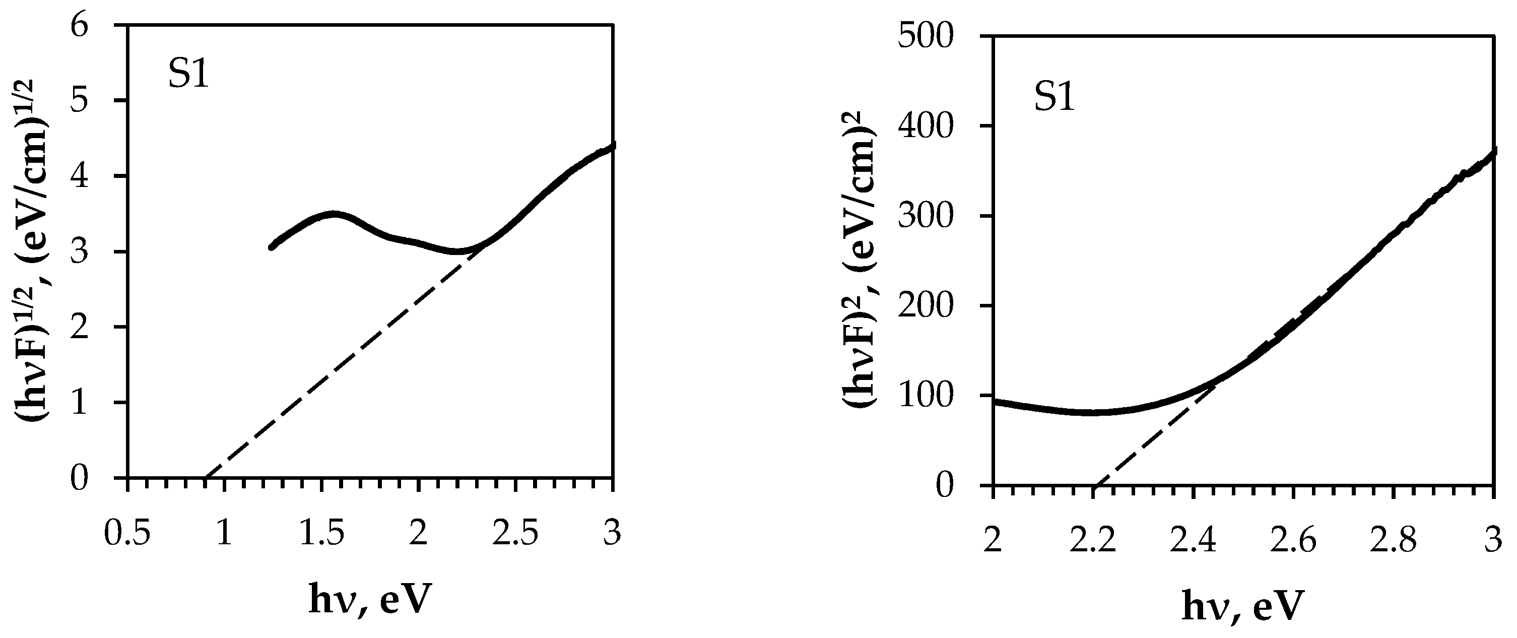
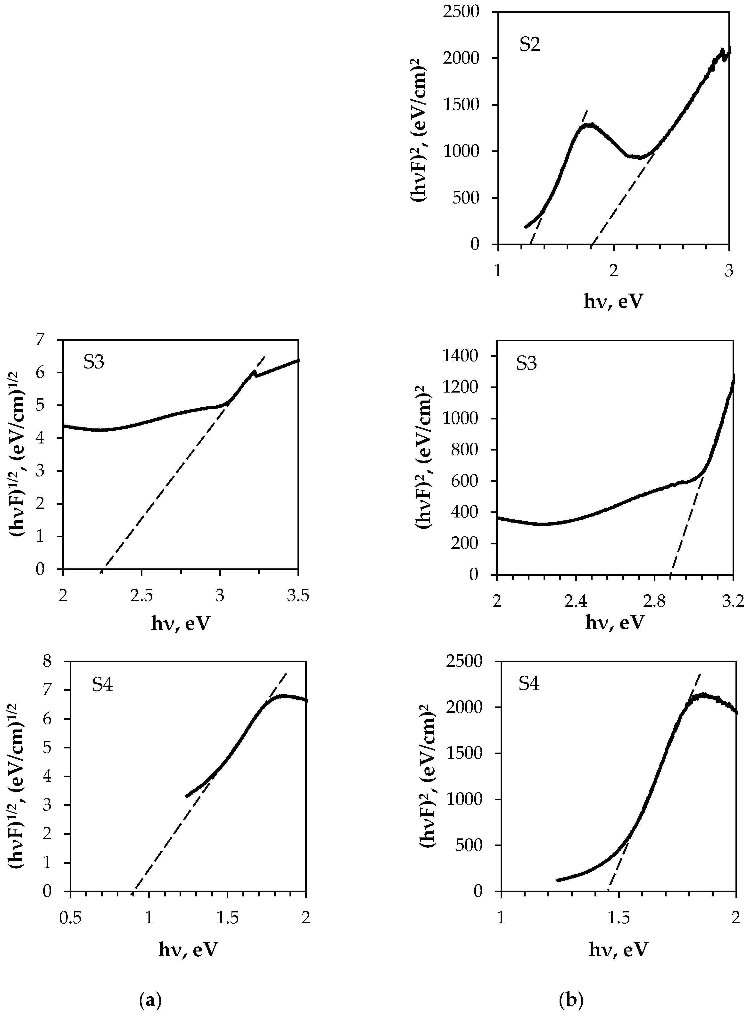
The bandgap energy of semiconducting materials depends on various factors, such as the growth technique and conditions, thickness, and type (e.g., bulk, thin film, or nanoparticles). Consequently, the bandgap energy of the same compounds varies. The indirect and direct optical energy gap (Eop) values of the obtained composites were determined from the intercept of the linear fit with the photon energy axis (see Figure 14). As can be seen, the Eop values of the samples differ greatly depending on the composition of both the textiles and the deposited thin films (see Table 5).
Bi2S3 films have two transitions on interaction with light: an indirect one at 1.03 eV [64], and a direct one at 1.3–1.7 eV [31,65]. This wide disparity in values is the result of varying stoichiometries, which in turn result from different deposition methods. The Bi2S3 thin films deposited by the SILAR method on the textiles under investigation exhibited the following direct-transition optical energy gap values: 1.58–1.68 eV [50].
CuxS have an experimentally observed indirect bandgap in range of 1.1–1.4 eV and a direct bandgap in range of 1.3–2.9 eV, depending on the material stoichiometry [66,67]. Moreover, this semiconductor exhibits near-metallic electrical conductivity due to the presence of copper vacancies, which act as electron acceptors and contribute free holes to the material’s valence band, thereby enhancing its electronic conductivity. CuS exhibits p-type conductivity, providing the compound with a remarkable potential for the design of heterojunctions [68].
Copper bismuth sulphide (Cu3BiS3) has p-type conductivity and an energy bandgap of 1.10–1.86 eV for direct transition [42,69] and 1.5–1.7 eV for indirect transition [70].
The direct optical energy gap values obtained from the fits (see Figure 14b) are consistent with the reported values for the Eop of multiphase Cu–Bi–S materials. The presence of two distinct Eop values (Figure 14b and Table 5) confirms that the S2 sample comprises two dominant semiconductor materials. The Eop value of 1.3 eV is similar to that of Cu–Bi sulphide compounds, while the value of 1.8 eV is similar to that of Ag nanoparticles [71] because Cu–Bi sulphide films were deposited on a polyamide textile metallised with silver. The highest Eop value for the S3 sample can be attributed to the Cu–Bi–S/Cu solid mixture. The indirect Eop values for the S1 and S4 samples were found to be 0.9 eV, i.e., about 0.2 eV lower than in other research. However, for the S3 sample, the Eop value was 2.25 eV, i.e., higher, similarly to the direct Eop value for this sample.
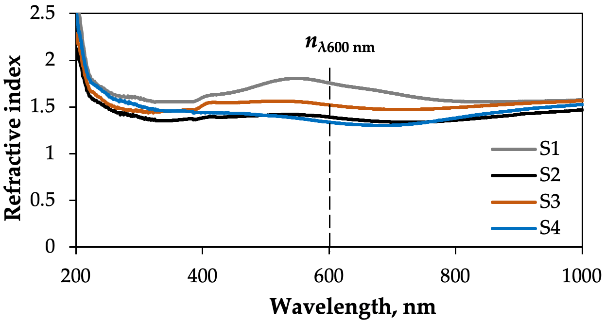
The refractive index (n) is a fundamental parameter for applying materials in optical equipment due to its direct relationship with energy dispersion. According literature data [72] the refractive index of Cu–Bi–S thin films varies depending on their composition and how they are deposited, but generally falls within the range of 1.4 to 2.5. The values of copper-doped bismuth sulphide films are between 1.4 and 1.8. The refractive index is significantly influenced by the specific copper-to-bismuth ratio, film thickness, and crystal phase (e.g., Bi2S3 vs. Cu3BiS3) absorption.
CuS thin films exhibit a higher refractive index, potentially around 2.31–2.64, while other copper sulphide (CuxS) compounds may show lower values like 2.07–2.26 [73,74].
Figure 15 shows the variation in the refractive index (n) of the S1–S4 samples within the 200–1000 nm wavelength range. The spectral behaviour of the refractive indices of the obtained composites was very similar within the wavelength regions of 200–400 nm and 800–1000 nm. They are approximately 1.5. However, obvious differences can be seen in the 400–800 nm region.
Table 5 presents a summary of the obtained data.
In our opinion, differences in the refractive index are related to the composition of textiles and films. The n value of a material depends greatly on the density of its electrons and how tightly they are bound to the atomic nucleus. Cu–Bi–S films contain various types of semiconductor, such as CuS, Cu3BiS3 and Bi2S3. Due to differences in the density of free electrons, the refractive index of each material varies. The volume fraction ratio of each phase to the film’s total volume also varies. It should also be noted that other interesting effects may occur in Cu–Bi–S films, and that the refractive index of the multiphase material cannot be predicted simply by interpolating the corresponding parameters of the pure phases.
Composite materials with an optical energy gap and refractive index obtained through the manufacturing process can be suitable for use in optical non-volatile memories, optical waveguides, and solar cells with improved efficiency, as these values are typical of standard lens materials.

4. Conclusions

Compact, multiphase Cu–Bi sulphide semiconductor nanocomposites were synthesised simultaneously on various textiles using the SILAR method. The results obtained imply that the surface morphology and elemental and phase composition of the nanocomposites, as well as their optical properties, were sensitive to the textiles used for thin film deposition. Scanning electron microscopy (SEM) analysis confirmed the development of a highly complex surface consisting of flake-like sub-micron structures and agglomerates. Deposition onto PET/PVC and C/PES/S textile samples with normalised atomic percentages of Cu (57.66–58.7%), Bi (3.71–5.0%) and S (36.3–38.63%) resulted in the formation of a large, non-uniform crystalline layer. In contrast, the analysis of thin films deposited onto PA/Ag and PA/Cu textile samples with normalised atomic percentages of Cu (63.78–68.75%), Bi (1.19–5.26%) and S (30.06–30.96%) suggested the formation of a homogeneous thin film with low surface resistivity of 30 Ω/sq and 52 Ω/sq, respectively.
Energy dispersive spectroscopy (EDX) confirmed the presence of copper, bismuth and sulphur. A higher Cu content was observed in all of the composite samples obtained, which distinctly suggests the dominance of copper sulphide compounds. The X-ray diffraction (XRD) analysis data are consistent with the EDX results and suggest that the deposited thin films are copper-rich. Consequently, the predominant phases in the deposited multiphase thin films are CuS and Cu3BiS3.
The direct optical band gap (Eop) was found to be 1.38–2.88 eV and the indirect to be 0.9–2.25 eV. The variation in band gap depends on the textile substrate used, as well as the volume fraction ratio of each phase (CuS, Bi2S3 and Cu3BiS3) to the film’s total volume. The refractive indices are also influenced by the composition of the textiles and films. Optical analysis indicated that Cu–Bi–S thin films are a suitable flexible absorber material for photovoltaic applications due to their suitable band gap and high optical absorption in the visible spectrum. The results presented are promising for optimising the fabrication process of Cu–Bi sulphide/textile nanocomposites, which are one of the most important components in flexible electronics.
The results suggest that future research should focus on selecting appropriate textiles, as well as optimising the bismuth sulphide deposition process, in order to achieve the desired Eop. This would prove the obtained composites to be valuable for utilisation.

Author Contributions

Conceptualization, V.K. methodology, V.K. and V.S.; software, V.S.; formal analysis, V.S.; investigation, V.K.; data curation, V.K.; writing—original draft preparation, V.K.; supervision, V.K.; funding acquisition, V.K. All authors have read and agreed to the published version of the manuscript.

Funding

This research was funded by the Lithuanian Research Council through its funding of student research and internships, Grant No. S-SV-25-272.

Institutional Review Board Statement

Not applicable.

Data Availability Statement

The original contributions presented in this study are included in the article. Further inquiries can be directed to the corresponding author.

Conflicts of Interest

The authors declare no conflicts of interest.

References

  1. Graham, E.; Fulghum, N.; Altieri, K. Global Electricity Review 2025. Ember. 8 April 2025. Available online: https://ember-energy.org/latest-insights/global-electricity-review-2025 (accessed on 22 September 2025).
  2. Ojstršek, A.; Plohl, O.; Gorgjeva, S.; Kurečič, M.; Jančič, U.; Hribenik, S.; Fakin, D. Metallisation of textiles and protenction of conductive layers: An overview of application techniques. Sensors 2021, 21, 3508. [Google Scholar] [CrossRef]
  3. Choudhury, K.; Tsianou, M.; Alexandridis, P. Recycling of Blended Fabrics for a Circular Economy of Textiles: Separation of Cotton, Polyester, and Elastane Fibres. Sustainability 2024, 16, 6206. [Google Scholar] [CrossRef]
  4. Zhong, H.; Bai, S.; Zou, B. Tuning the luminescence properties of colloidal I-III-VI semiconductor nanocrystals for optoelectronics and biotechnology applications. J. Phys. Chem. Lett. 2012, 3, 3167–3175. [Google Scholar] [CrossRef]
  5. Talapin, D.V.; Lee, J.S.; Kovalenko, M.V.; Shevchenko, E.V. Prospects of colloidal nanocrystals for electronic and optoelectronic applications. Chem. Rev. 2010, 110, 389–458. [Google Scholar] [CrossRef] [PubMed]
  6. Manimegalai, D.K.; Manikandan, A.; Moortheswaran, S.; Antony, S.A. One-pot microwave irradiation synthesis and characterization studies of nanocrystalline CdS photocatalysts. Adv. Sci. Eng. Med. 2015, 7, 722–727. [Google Scholar] [CrossRef]
  7. Manikandan, A.; Antony, S.A. A novel approach for the synthesis and characterization studies of Mn2+-Doped CdS nano-crystals by a facile microwave-assisted combustion method. J. Supercond. Nov. Magn. 2014, 27, 2725–2733. [Google Scholar] [CrossRef]
  8. Lou, Y.; Chen, X.; Samia, A.C.; Burda, C. Femtosecond Spectroscopic Investigation of the Carrier Lifetimes in Digenite Quantum Dots and Discrimination of the Electron and Hole Dynamics via Ultrafast Interfacial Electron Transfer. J. Phys. Chem. B 2003, 107, 12431–12437. [Google Scholar] [CrossRef]
  9. Chung, J.S.; Sohn, H.J. Electrochemical behaviors of CuS as a cathode material for lithium secondary batteries. J. Power Sources 2002, 108, 226–231. [Google Scholar] [CrossRef]
  10. Deb, S.; Kalita, P.K. Green synthesis of copper sulfide (CuS) nanostructures for heterojunction diode applications. J. Mater. Sci. Mater. Electron. 2021, 32, 24125–24137. [Google Scholar] [CrossRef]
  11. Chen, X.; Wang, T.; Shi, J.; Lv, W.; Han, Y.; Zeng, M.; Yang, J.; Hu, N.; Su, Y.; Wei, H.; et al. A Novel Artificial Neuron-Like Gas Sensor Constructed from CuS Quantum Dots/Bi2S3 Nanosheets. Nano-Micro Lett. 2022, 14, 8. [Google Scholar] [CrossRef] [PubMed]
  12. Heiba, Z.K.; Deyab, M.A.; Mohamed, M.B.; Farag, N.M.; El-naggar, A.M.; Plaisier, J.R. Electrochemical performance of CuCo2O4/CuS nanocomposite as a novel electrode material for supercapacitor. Appl. Phys. A 2021, 127, 853. [Google Scholar] [CrossRef]
  13. Liang, W.; Whangbo, M.H. Conductivity anisotropy and structural phase transition in Covellite CuS. Solid State Commun. 1993, 85, 405. [Google Scholar] [CrossRef]
  14. Gopi, C.V.V.M.; Sambasivam, S.; Vinodh, R.; Kim, H.J.; Obaidat, I.M. Nanostructured Ni-doped CuS thin film as an efficient counter electrode material for high–performance quantum dot–sensitized solar cells. J. Mater. Sci. Mater. Electron. 2020, 31, 975–982. [Google Scholar] [CrossRef]
  15. Huse, N.P.; Dive, A.S.; Gattu, K.P.; Sharma, R. An experimental and theoretical study on soft chemically grown CuS thin film for photosensor application. Mater. Sci. Semicond. Process. 2017, 67, 62–68. [Google Scholar] [CrossRef]
  16. Ain, N.; Nasir, J.A.; Khan, Z.; Butler, I.S.; Rehman, Z. Copper sulfide nanostructures: Synthesis and biological applications. RSC Adv. 2022, 12, 7550–7567. [Google Scholar] [CrossRef]
  17. Mao, G.; Dong, W.; Kurth, D.G.; Mohwald, H. Synthesis of Copper Sulfide Nanorod Arrays on Molecular Templates. Nano Lett. 2004, 4, 249–252. [Google Scholar] [CrossRef]
  18. Folmer, J.C.W.; Jellinek, F. The valence of copper in sulphides and selenides: An X-ray photoelectron spectroscopy study. J. Less Common Met. 1980, 76, 153–162. [Google Scholar] [CrossRef]
  19. Han, Y.; Wang, Y.; Gao, W.; Wang, Y.; Jiao, L.; Yuan, H.; Liu, S. Synthesis of novel CuS with hierarchical structures and its application in lithium-ion batteries. Powder Technol. 2011, 212, 64–68. [Google Scholar] [CrossRef]
  20. Lai, C.H.; Huang, K.W.; Cheng, J.H.; Lee, C.Y.; Hwang, B.J.; Chen, L.J. Direct growth of high-rate capability and high capacity copper sulfide nanowire array cathodes for lithium–ion batteries. J. Mater. Chem. 2010, 20, 6638–6645. [Google Scholar] [CrossRef]
  21. Mane, R.S.; Lokhande, C.D. Chemical deposition method for metal chalcogenide thin films. Mater. Chem. Phys. 2000, 65, 1–31. [Google Scholar] [CrossRef]
  22. Saranya, M.; Santhosh, C.; Prathap Augustine, S.; Nirmala Grace, A. Synthesis and characterication of CuS nanomaterials using hydrothermal route. J. Exp. Nanosci. 2014, 9, 329–336. [Google Scholar] [CrossRef]
  23. Deady, E.; Moon, C.; Moore, K.; Goodenough, K.M.; Shail, R.K. Bismuth: Economic geology and value chains. Ore Geol. Rev. 2022, 143, 104722. [Google Scholar] [CrossRef]
  24. Onwudiwe, D.C.; Nkwe, V.M. Morphological variations in Bi2S3 nanoparticles synthesized by using single source precursor. Heliyon 2020, 6, e04505. [Google Scholar] [CrossRef]
  25. Renuka Devee, D.; Sivanesan, T.; Muthukrishnan, R.M.; Pourkodee, D.; Mohammed Yusuf Ansari, P.; Abdul Kader, S.M.; Raniani, R.A. A novel photocatalytic activity of Bi2S3 nanoparticles for pharmaceutical and organic pollution removal in water remediation. Chem. Phys. Impact 2024, 8, 100605. [Google Scholar] [CrossRef]
  26. Razavi, F.S.; Mahdi, M.A.; Ghanbari, D.; Dawi, E.A.; Abed, M.J.; Ganduh, S.H.; Jasmin, L.S.; Salavati-Niasari, M. Fabrication and design of four-component Bi2S3/CuFe2O4/Cu2O nanocomposite as new active materials for high performance electrochemical hydrogen storage application. J. Energy Storage 2024, 94, 113493. [Google Scholar] [CrossRef]
  27. Yu, Y.; Hu, Z.; Lien, S.Y.; Yu, Y.; Gao, P. Self-powered thermoelectric hydrogen sensors based on low-cost bismuth sulphide thin films: Quick response at room temperature. ACS Appl. Mater. Interfaces 2022, 14, 47696–47705. [Google Scholar] [CrossRef] [PubMed]
  28. Kan, H.; Yang, W.; Guo, Z.; Li, M. Highly sensitive room-temperature NO2 gas sensor based on Bi2S3 nanorods. J. Mater. Sci. Mater. Electron. 2024, 35, 331. [Google Scholar] [CrossRef]
  29. Rong, P.; Gao, S.; Ren, S.; Lu, H.; Yan, J.; Li, L.; Zhang, M.; Han, Y.; Jiao, S.; Wang, J. Large-area freestanding Bi2S3 nanofibrous membranes for fast photoresponse flexible IR imaging photodetector. Adv. Funct. Mater. 2023, 33, 2300159. [Google Scholar] [CrossRef]
  30. Singh, A.; Chauhan, P.; Verma, A.; Yadav, B.C. Interfacial engineering enables polyaniline-decorated bismuth sulphide nanorods towards ultrafast metal-semiconductor-metal UV-Vis broad spectra photodetector. Adv. Compos. Hybrid Mater. 2024, 7, 88. [Google Scholar] [CrossRef]
  31. Supekar, A.T.; Bhujbal, P.K.; Salunke, S.A.; Rathod, S.M.; Patole, S.P.; Pathan, H.M. Bismuth sulphide and antimony sulphide-based solar cells: A review. ES Energy Environ. 2023, 19, 848. [Google Scholar] [CrossRef]
  32. Yu, X.L.; Cao, C.B. Photoresponse and field-emission properties of bismuth sulphide nanoflowers. Cryst. Growth Des. 2008, 8, 3951–3955. [Google Scholar] [CrossRef]
  33. Yu, Y.; Jin, C.H.; Wang, R.H.; Chen, Q.; Peng, L.M. High-quality ultralong Bi2S3 nanowires: Structure, growth, and properties. J. Phys. Chem. B 2005, 109, 18772–18776. [Google Scholar] [CrossRef]
  34. Ajiboye, T.O.; Onwudiwe, D.C. Bismuth sulphide based compounds: Properties, synthesis and applications. Results Chem. 2021, 3, 100151. [Google Scholar] [CrossRef]
  35. Onwudiwe, D.C.; Ovewo, O.A.; Atamtürk, U.; Ojelere, O.; Mathur, S. Photocatalytic reduction of Cr(VI) using star-shaped Bi2S3 obtained from microwave irradiation of bismuth complex. J. Environ. Chem. Eng. 2020, 8, 103816. [Google Scholar] [CrossRef]
  36. Zhang, M.; Chen, D.J.; Wang, R.Z.; Feng, J.J.; Bai, Z.; Wang, A.J. D-penicillanime assited hydrothermal synthesis of Bi2S3 nanoflowers and their electrochemical application. Mater. Sci. Eng. 2013, 33, 3980–3985. [Google Scholar] [CrossRef]
  37. Terdalkar, P.; Kumbhar, D.D.; Pawar, S.D.; Nirmal, K.A.; Kim, T.G.; Mukherjee, S.; Khot, K.V.; Dongale, T.D. Revealing switching statistics and artificial synaptic properties of Bi2S3 memristor. Solid State Electron. 2025, 225, 109076. [Google Scholar] [CrossRef]
  38. Zhao, Y.; Tao, Y.; Huang, Q.; Huang, J.; Kuang, J.; Gu, R.; Zeng, P.; Li, H.-Y.; Liang, H.; Liu, H. Electrochemical Biosensor Employing Bi2S3 Nanocrystals-Modified Electrode for Bladder Cancer Biomarker Detection. Chemosensors 2022, 10, 48. [Google Scholar] [CrossRef]
  39. Yang, Z.; Wang, L.; Zhang, J.; Liu, J.; Yu, X. Application of bismuth sulphide based nanomaterials in cancer diagnosis and treatment. Nano Today 2023, 49, 101799. [Google Scholar] [CrossRef]
  40. Zhang, X.; Xie, J.; Tang, Y.; Lu, Z.; Hu, J.; Wang, Y.; Cao, Y. Oxygen self-doping Bi2S3@C spheric successfully enhanced long-term performance in lithium-ion batteries. ACS Appl. Mater. Interfaces 2024, 16, 52423–52431. [Google Scholar] [CrossRef]
  41. Fang, Y.; Zhao, W.; Li, W.; Han, X. Effects of thiourea dosage on the structural, optical and electrical properties of one–step solution processed Cu3BiS3 film for photovoltaics. Appl. Phys. A 2021, 127, 9. [Google Scholar] [CrossRef]
  42. Deshmukh, S.G.; Kheraj, V. A comprehensive review on synthesis and characterizations of Cu3BiS3 thin films for solar photovoltaics. Nanotechnol. Environ. Eng. 2017, 2, 15. [Google Scholar] [CrossRef]
  43. Yang, Y.; Xiong, X.; Yin, H.; Zhao, M.; Han, J. Study of copper bismuth sulfide thin films for the photovoltaic application. J. Mater. Sci. Mater. Electron. 2018, 30, 1832–1837. [Google Scholar] [CrossRef]
  44. Shankar, E.G.; Ramulu, B.; Nagaraju, M.; Yu, J.S. Electrochemically triggered rational design of bismuth copper sulfide for wearable all–sulfide semi–solid–state supercapacitor with a wide operational potential window (1.8V) and ultra–long life. Inorg. Chem. Front. 2024, 11, 3270–3284. [Google Scholar] [CrossRef]
  45. Santos, D.R.; Shukla, S.; Vermang, B. Prospects of copper–bismuth chalcogenide absorbers for photovoltaics and photoelectrocatalysis. J. Mater. Chem. A 2023, 11, 22087–22104. [Google Scholar] [CrossRef]
  46. Parra-Arciniega, S.M.; Garcia-Gomez, N.A.; Garza-Toyar, L.L.; García-Gutiérrez, D.I.; Sánchez, E.M. Ultrasonic irradiation-assisted synthesis of Bi2S3 nanoparticles in aqueous ionic liquid at ambient condition. Ultrason. Sonochem. 2017, 36, 95–100. [Google Scholar] [CrossRef] [PubMed]
  47. Ran, Y.; Song, Y.; Jia, X.; Gu, P.; Cheng, Z.; Zhu, Y.; Wang, Q.; Pan, Y.; Li, Y.; Gao, Y.; et al. Large-Scale Vertically Interconnected Complementary Field-Effect Transistors Based on Thermal Evaporation. Small 2024, 20, 2309953. [Google Scholar] [CrossRef]
  48. Bouachri, M.; Oubakalla, M.; El Farri, H.; Diaz-Guerra, C.; Mhalla, J.; Zimou, J.; El-Habib, A.; Beraich, M.; Nouneh, K.; Fahoume, M.; et al. Substrate temperature effects on the structural, morphological and optical properties of Bi2S3 thin films deposited by spray pyrolysis: An experimental and first-principles study. Opt. Mater. 2023, 135, 113215. [Google Scholar] [CrossRef]
  49. Rodriguez-Rosales, K.; Cruz-Gomez, J.; Cruz, J.S.; Guillen-Cervantes, A.; de Moure-Flores, F.; Villagran-Muniz, M. Plasma emission spectroscopy for studying Bi2S3 produced by pulsed laser deposition and effects of substrate temperature on structural, morphological, and optical properties of thin films. Mater. Sci. Eng. B 2025, 312, 117867. [Google Scholar] [CrossRef]
  50. Sruogaite, V.; Krylova, V. Formation and Study of Bismuth Sulphide Thin Films on Textiles of Different Compositions. Appl. Sci. 2025, 15, 9904. [Google Scholar] [CrossRef]
  51. Sartale, S.D.; Lokhande, C.D. Growth of copper sulphide thin films by successive ionic layer adsorption and reaction (SILAR) method. Mater. Chem. Phys. 2000, 65, 63–67. [Google Scholar] [CrossRef]
  52. Carillo, A.; Rivas-Valles, B.G.; Castillo, S.J.; Ramirez, M.M.; Luque-Morales, P.A. New formulation to synthesize semiconductor Bi2S3 thin films using chemical bath deposition for optoelectronic applications. Symmetry 2022, 14, 2487. [Google Scholar] [CrossRef]
  53. Nandihalli, N. Thermoelectric films and periodic structures and spin Seebeck effect systems: Facets of performance optimization. Mater. Today Energy 2022, 25, 100965. [Google Scholar] [CrossRef]
  54. Hobbs, P.V. Basic Physical Chemistry for the Atmospheric Sciences, 2nd ed.; Cambridge University Press: Cambridge, UK, 2000; ISBN 9780521785679. 222p. [Google Scholar]
  55. López, R.; Gómez, R. Band-gap energy estimation from diffuse reflectance measurements on sol-gel and commercial TiO2: A comparative study. J. Sol-Gel Sci. Technol. 2012, 61, 1–7. [Google Scholar] [CrossRef]
  56. Nasr, M.; Viter, R.; Eid, C.; Warmont, F.; Habchi, R.; Miele, P.; Bechelany, M. Synthesis of novel ZnO/ZnAl2O4 multi co-centric nanotubes and their long-term stability in photocatalytic application. RSC Adv. 2016, 6, 103692–103699. [Google Scholar] [CrossRef]
  57. Loste, J.; Lopez-Cuesta, J.-M.; Billon, L.; Garay, H.; Save, M. Transparent polymer nanocomposites: An overview on their synthesis and advanced properties. Prog. Polym. Sci. 2019, 89, 133–158. [Google Scholar] [CrossRef]
  58. Rashad, M. Tuning the optical properties of polyvinyl alcohol doped with different metal oxide nanoparticles. Opt. Mater. 2020, 105, 109857. [Google Scholar] [CrossRef]
  59. Krylova, V.; Dukštienė, N.; Markevičiūtė, H. Ag-Se/Nylon Nanocomposites Grown by Template-Engaged Reaction: Microstructures, Composition, and Optical Properties. Nanomaterials 2022, 12, 2584. [Google Scholar] [CrossRef]
  60. Mina, M.S.; Kabir, H.; Rahman, M.M.; Kabir, M.A.; Rahaman, M.; Bashar, M.S.; Islam, M.S.; Sharmin, A.; Ahmed, F. Optical and Morphological Characterization of BaSe Thin Films Synthesized via Chemical Bath Deposition. IOSR J. Appl. Phys. 2013, 4, 30–35. [Google Scholar] [CrossRef]
  61. Rincón, M.E.; Campos, J.; Suárez, R. A comparison of the various thermal treatments of chemically deposited bismuth sulfide thin films and the effect on the structural and electrical properties. J. Phys. Chem. Solids 1999, 60, 385–392. [Google Scholar] [CrossRef]
  62. Si, J.; Ma, R.; Wu, Y.; Dong, Y. Microstructure and magnetic properties of novel powder cores composed of iron-based amorphous alloy and PTFE. J. Mater. Sci. 2022, 57, 8154–8166. [Google Scholar] [CrossRef]
  63. Goncalves, G.; Marques, P.A.; Pinto, R.J.; Trindade, T.; Neto, C.P. Surface modification of cellulosic fibres for multi-purpose TiO2 based nanocomposites. Compos. Sci. Technol. 2009, 69, 7–8. [Google Scholar] [CrossRef]
  64. Mahuli, N.; Saha, D.; Sarkar, S.K. Atomic Layer Deposition of p-Type Bi2S3. Phys. Chem. C 2017, 121, 14–8136. [Google Scholar] [CrossRef]
  65. Nambiar, S.; Osei, E.K.; Yeow, J.T.W. Bismuth sulfide nanoflowers for detection of X-rays in the mammographic energy range. Sci. Rep. 2015, 5, 9440. [Google Scholar] [CrossRef]
  66. Xu, Q.; Huang, B.; Zhao, Y.; Yan, Y.; Noufi, R.; Wei, S.H. Crystal and electronic structures of CuxS solar cell absorbers. Appl. Phys. Lett. 2012, 100, 061906. [Google Scholar] [CrossRef]
  67. Oppong-Antwi, L.; Gunawan, D.; Toe, C.Y.; Yao, Y.; Valanoor, N.; Hart, J.N. CuxS films as photoelectrodes for visible-light water splitting. Mater. Sci. Semicond. Process. 2024, 184, 108833. [Google Scholar] [CrossRef]
  68. Mohammed, K.A.; Ahmed, S.M.; Mohammed, R.Y. Investigation of Structure, Optical, and Electrical Properties of CuS Thin Films by CBD Technique. Crystals 2020, 10, 684. [Google Scholar] [CrossRef]
  69. Fazal, T.; Iqbal, S.; Shah, M.; Elkaeed, E.B. Optoelectronic, structural and morphological analysis of Cu3BiS3 sulfosalt thin films. Res. Phys. 2022, 36, 105453. [Google Scholar] [CrossRef]
  70. Kumar, M.; Persson, C. Ternary Cu3BiY3 (Y = S, Se, and Te) for Thin-Film Solar Cells. MRS Online Proc. Libr. 2013, 1538, 235–240. [Google Scholar] [CrossRef]
  71. Hlapisi, N.; Ajibade, P.A. Preparation of pure phase silver nanoparticles: Morphological, optical, binding interactions with bovine serum albumin and antioxidant potential studies. J. Mol. Struct. 2025, 1322, 140219. [Google Scholar] [CrossRef]
  72. Fazal, T.; Ismail, B.; Wafee, S.; Kambooh, A.H.; Khan, A.R. Cu doped Bi2S3 as potential absorbers for thin film solar cells: Optical and structural properties. Chalcogenide Lett. 2016, 13, 225–231. [Google Scholar]
  73. Erken, O.; Gunes, M.; Kirmizigul, F.; Gumus, C. Investigation of properties the copper sulfide thin films prepared from different copper salts. Optik 2018, 168, 884–891. [Google Scholar] [CrossRef]
  74. Habiboglu, C.; Erken, O.; Gunes, M.; Yilmaz, O.; Cevlik, H.C.; Ulutas, C.; Gumus, C. Effect of molar concentration on the structural, linear and nonlinear optical properties of CuS (covellite) thin films. Solid State Commun. 2022, 352, 114823. [Google Scholar] [CrossRef]
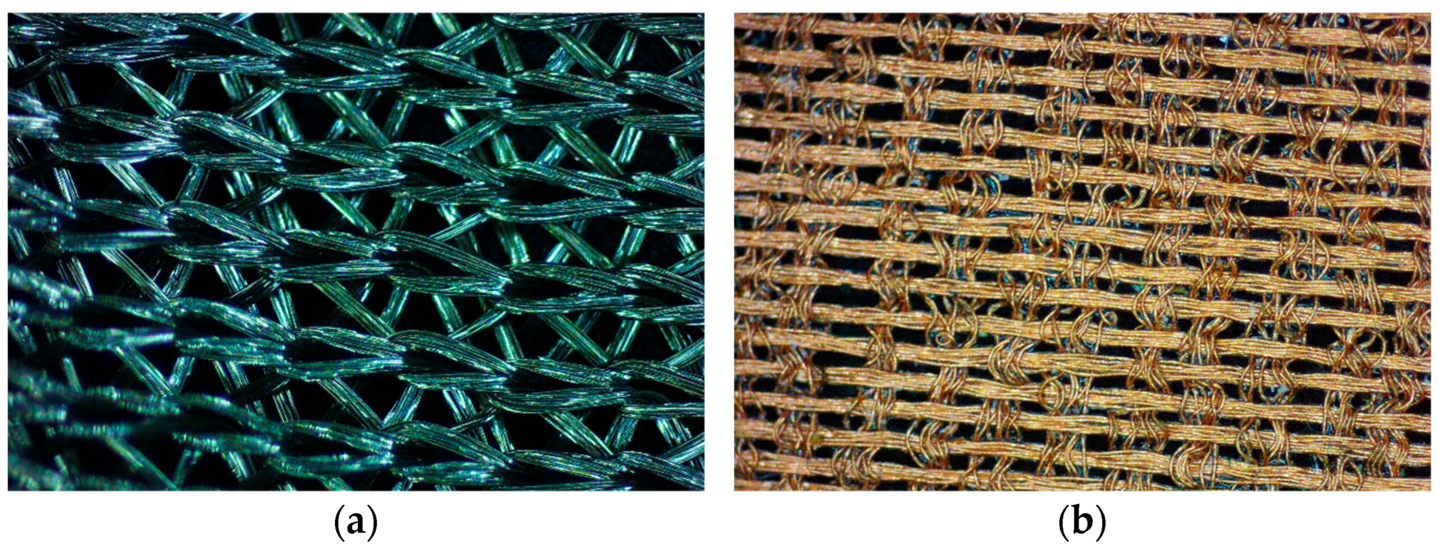
Figure 1. Textural views by stereo microscope: (a) PA/Ag textile; (b) PA/Cu textile. Zoom magnification is 3.2×.
Coatings 15 01266 g001
Figure 2. Textural views by optical microscope: (a) PET/PVC textile; (b) C/PES/S textile. Zoom magnification is 100×.
Coatings 15 01266 g002
Figure 3. XRD diffractogram of Bi2S3 sediment, CuS sediment and sample S1. Peaks are labelled as follows: ●—rhombohedral CaCO3 (JCPDS: 05-0586); ○—tetragonal TiO2 (JCPDS: 04-006-1890); □—orthorhombic Bi2S3 (JCPDS: 17-320); ▼—hexagonal CuS (JCPDS: 78-0876); *—orthorhombic Cu3BiS3 (JCPDS: 43-1479).
Coatings 15 01266 g003
Figure 4. XRD diffractogram of sample S2. Peaks are labelled as follows: Δ—PA6 (JCPDS: 12-923); ○—Ag (JCPDS: 04-0783); ▼—hexagonal CuS (JCPDS: 78-0876); □—orthorhombic Bi2S3 (JCPDS: 17-320); *—orthorhombic Cu3BiS3 (JCPDS: 43-1479).
Coatings 15 01266 g004
Figure 5. XRD diffractogram of sample S3. Peaks are labelled as follows: Δ—PA6 (JCPDS: 12-923); ▼—hexagonal CuS (JCPDS: 78-0876); □—orthorhombic Bi2S3 (JCPDS: 17-320); *—orthorhombic Cu3BiS3 (JCPDS: 43-1479).
Coatings 15 01266 g005
Figure 6. XRD diffractogram of sample S4. Peaks are labelled as follows: Δ—cellulose I (JCPDS: 03-0226); ▼—hexagonal CuS (JCPDS: 78-0876); □—orthorhombic Bi2S3 (JCPDS: 17-320); *—orthorhombic Cu3BiS3 (JCPDS: 43-1479).
Coatings 15 01266 g006
Figure 7. SEM images of the S1 sample: (a)—50× magnified; (b)—1000× magnified; (c)—4000× magnified; (d)—10,000× magnified.
Coatings 15 01266 g007
Figure 8. SEM images of the S2 sample: (a)—50× magnified; (b)—1000× magnified; (c)—4000× magnified; (d)—10,000× magnified.
Coatings 15 01266 g008aCoatings 15 01266 g008b
Figure 9. SEM images of the S3 sample: (a)—50× magnified; (b)—1000× magnified; (c)—4000× magnified; (d)—10,000× magnified.
Coatings 15 01266 g009
Figure 10. SEM images of S4 sample: (a)—50× magnified; (b)—1000× magnified; (c)—4000× magnified; (d)—10,000× magnified.
Coatings 15 01266 g010
Figure 11. EDX results relating to the S1–S4 samples: (a) Representative EDX spectra. The normalised atomic percentages of Cu, Bi and S in the films are shown in the corresponding insets; (b) Chemical elemental maps of Cu (red), Bi (green) and S (blue), 5000× magnified.
Coatings 15 01266 g011
Figure 12. Optical diffuse reflectance spectra of the investigated textile sample as a function of wavelength in the range of 200–800 nm.
Coatings 15 01266 g012
Figure 13. Optical diffuse reflectance spectra as a function of wavelength, ranging from 200 to 1000 nm, for obtained composites.
Coatings 15 01266 g013
Figure 14. Optical energy gap determination from diffuse reflectance spectra by the Kubelka–Munk method: (a) indirect transition; (b) direct transition.
Coatings 15 01266 g014aCoatings 15 01266 g014b
Figure 15. Refractive index as a function of wavelength, ranging from 200 to 1000 nm, of the obtained composites.
Coatings 15 01266 g015
Table 1. Characteristics of investigated commercial textiles.
Textile CompositionColourThickness, mmBasis Weight, g/m2Heat Resistance, °CCold Resistance, °CSurface Resistivity, Ω/sqManufacturer
YarnCoating
PET *PVCwhite0.56850+70−30Verseidag-Indutex GmbH, Krefeld, Germany
PAAgmetallic-grey0.1034 ± 2+70−304.4Kufner Holding GmbH, Unterhaching, Germany
PACured-brown0.0552 ± 5+70−302.4Kufner Holding GmbH, Unterhaching, Germany
C/PES/S **green0.35290+80−30Mianyang Jialian Printing and Dyeing Co., Ltd., Mianyang, China
* PET fabric, double-sided PVC coating and lacquer, upside high-gloss embossed, flame retardant acc. to DIN 75 200, free of cadmium. ** The most commonly used spandex fibre is made up of at least 85% polyurethane and 15% other materials, such as nylon or polyester.
Table 2. The reagents used in the research.
ReagentCAS No.Purity, wt%Supplier
NameFormula
Sulphuric acidH2SO47664–93–9≥96Eurochemicals *
Orthophosphoric acidH3PO47664–38–2≥60Eurochemicals *
Chromium trioxideCrO31333–82–0≥97Sigma–Aldrich **
Bismuth nitrate pentahydrateBi(NO3)3 × 5H2O10035-06-0≥99Sigma–Aldrich **
Copper sulphate pentahydrateCuSO4 × 5H2O7758-99-8≥99Eurochemicals *
Sodium thiosulfate pentahydrateNa2S2O3 × 5H2O7757–83–7≥98Sigma–Aldrich **
* UAB Eurochemicals, Vilnius, Lithuania. ** Sigma-Aldrich Chemie GmbH, Munich, Germany.
Table 3. Thin films of copper bismuth sulphide deposition conditions.
Semiconductor Precursors Solution Concentration and TemperatureNumber
of Cycles
0.05 M Na2S2O3
20 ± 1 °C
0.1 M Bi(NO3)3
20 ± 1 °C
0.1 M CuSO4
69 ± 1 °C
Exposure time for one cycle, hBi2S3887
CuS1119
Table 4. Sample codes and description.
CodeCopper Bismuth Sulphide Is Deposited onto Textiles
S1mechanically roughened and thermo-oxidatively acid-treated polyethylene terephthalate fabric coated with polyvinyl chloride
S2100% nylon, metallised with silver
S3100% nylon, metallised with copper
S475% cotton, 24% polyester and 1% spandex
Table 5. Composition, optical energy gap values (Eop) and refractive indices (n) of the obtained composites.
SampleComposition from XRDComposition, at. % from EDXEop, eVnλ600 nm
CuBiSDirect TransitionIndirect Transition
S1hexagonal CuS,
orthorhombic Cu3BiS3,
orthorhombic Bi2S3
58.75.036.32.2 ± 0.010.9 ± 0.0151.76
S268.751.1930.061.3 ± 0.01
1.8 ± 0.02
1.39
S363.785.2630.962.88 ± 0.012.25 ± 0.011.52
S457.663.7138.631.45 ± 0.020.9 ± 0.011.34
Disclaimer/Publisher’s Note: The statements, opinions and data contained in all publications are solely those of the individual author(s) and contributor(s) and not of MDPI and/or the editor(s). MDPI and/or the editor(s) disclaim responsibility for any injury to people or property resulting from any ideas, methods, instructions or products referred to in the content.