Abstract
To address the issue in the pure oxide molten salt system Na2WO4-WO3, where the relatively high melting temperature often causes thermal corrosion of the base material and reduces electrodeposition efficiency. A new molten salt system for electrodeposition tungsten coatings on CuCrZr substrates at relatively low temperatures was investigated. The crystal structure and microstructure of the tungsten coatings were analyzed using X-ray diffraction (XRD), scanning electron microscopy (SEM), and energy-dispersive X-ray spectroscopy (EDS). The results indicate that the power supply mode, current density, and duty cycle significantly affect the microstructure, crystalline characteristics, and overall performance of the tungsten coating. Pure tungsten coatings were successfully fabricated on CuCrZr substrates at 943 K. The best electrodeposition parameters were determined to be a current density of 40 mA/cm2 and a duty cycle of 40%. Moreover, after prolonged electrodeposition (60 h), the tungsten coatings retained fine grains, with sizes ranging from 2 μm to 6 μm.
1. Introduction
Nuclear fusion energy is widely recognized as one of the most promising energy sources due to its advantages of abundant availability, environmental cleanliness, and high energy efficiency [1]. The material issue is the key factor determining whether controlled nuclear fusion can be ultimately achieved. Among nuclear fusion materials, plasma-facing materials and components (PFC, Plasma Facing Components) are considered to be the most important category. In the fusion reactor, PFC is directly exposed to the high-energy particles from the plasma edge. Tungsten metal has emerged as a leading candidate material for the first wall in modern tokamak devices, owing to its excellent physical properties, including a high melting point (3695 K), high thermal conductivity, minimal tritium retention, low vapor pressure (p = 1.3 × 10⁻⁷ Pa), a low coefficient of thermal expansion, and superior resistance to sputtering [2,3,4]. Copper-based heat sink materials possess excellent thermal conductivity and machinability, and can effectively transfer the high heat load on the surface materials of PFC. Therefore, they are selected as the heat sink materials in PFC. However, significant differences exist between the thermal expansion coefficients of tungsten and CuCrZr alloy (a commonly used heat sink material), posing considerable challenges in bonding dissimilar materials. In the fabrication of tungsten coatings, techniques such as plasma spraying (PS), chemical vapor deposition (CVD), and physical vapor deposition (PVD) [5] have been widely adopted. Specifically, the PS technique [6] is known for its simplicity and high efficiency; however, the resulting coatings often exhibit porosity or cracking due to the inherent characteristics of the process. The CVD method enables rapid deposition of tungsten but requires high-temperature conditions. Although PVD can produce high-quality, dense, and uniform tungsten coatings, it faces limitations in terms of cost and technical difficulty when depositing thick coatings [7]. In contrast, direct preparation of tungsten coatings on substrate surfaces via molten salt electrodeposition is considered a promising solution to this engineering challenge.
Electrodeposition in the Na2WO4-WO3 molten salt system can yield high-quality tungsten coatings with dense and uniform microstructures [8]. However, the relatively high melting temperature of this oxide-based system often leads to thermal corrosion of the substrate and reduces electrodeposition efficiency. Therefore, it is of great significance to search for a molten salt system that is compatible with more substrates to reduce the electrodeposition temperature and improve the electrodeposition efficiency for the development of tungsten coating preparation by molten salt electrodeposition. Fan Jiang et al. [9] successfully deposited tungsten coatings with low oxygen content on copper alloy substrates via pulse electroplating in the Na2WO4-WO3-NaPO3 molten salt system, achieving dense morphologies under various conditions. Ningbo Sun et al. [10] conducted tungsten electrodeposition in the Na2WO4-WO3 molten salt at 1173 K. Yusha Li et al. [11] fabricated a 433.72 µm tungsten coating on a CuCrZr alloy substrate via pulse current electrodeposition using a Na2WO4-WO3-KCl-NaF molten salt system at an electrodeposition temperature of 1053 K. This coating exhibited high density, absence of impurities, excellent adhesion to the substrate, and superior stability and durability. To reduce the electrodeposition temperature, some researchers have explored halide-based molten salt systems, such as NaCl-KCl-NF-WO3 [12] and LiF-KCl-Li2WO4 [13]. In this study, a KCl-KF-WO3 molten salt system was designed for tungsten electrodeposition at 943 K. By optimizing the power supply mode, current density, duty cycle, and electrodeposition time, the halide-oxide KCl-KF-WO3 molten salt system successfully produced tungsten coatings with fine grains, uniform microstructure, and high density on CuCrZr substrates. A systematic investigation was also conducted to evaluate the influence of process parameters within this moderate-temperature molten salt system on the phase composition, microstructure, and properties of the resulting tungsten coatings.
2. Experiment and Parameters
2.1. Coating Deposition
In this experiment, a metallic tungsten coating was prepared using the molten salt electrodeposition technique. The molten salt system employed was composed of KF-KCl-WO3. The WO3 (purity: 99.5%, Tianjin FuChen Chemical Reagent Co., Ltd., Tianjin, China), KCl (purity: 99%, Macklin Biochemical Technology Co., Ltd., Shanghai, China), and KF (purity: 99%, Macklin Biochemical Technology Co., Ltd., Shanghai, China) used in the experiment were all analytical-grade reagents. KF, KCl, and WO3 were individually dried at 473 K for 12 h in a vertical furnace. Subsequently, the pre-dried reagents were weighed in a predetermined molar ratio of 1.2:1:0.1 (KF:KCl:WO3) and thoroughly mixed in a ball mill before being loaded into a graphite crucible. The crucible was then placed inside a reaction vessel, which was positioned in an electric furnace. The CuCrZr alloy served as the anode electrode, while a tungsten plate (purity: 99.99%, Beijing Tianlong Tungsten & Molybdenum Technology Co., Ltd., Beijing, China) was used as the cathode electrode. The crucial role of selecting tungsten as the anode is to precisely replenish tungsten ions. In the KCl-KF-WO3 molten salt system, the tungsten ions required for electro-deposition mainly come from the dissolution of the anode tungsten. The reaction can be understood as follows: At the anode, the tungsten block is oxidized to tungsten ions and enters the molten salt; these ions then form active ions in the molten salt and migrate to the cathode; at the cathode, the active ions are reduced to metallic tungsten and deposited on the substrate. This is a self-consuming equilibrium process, where the dissolution rate of the anode tungsten matches the deposition rate of the cathode tungsten, which is crucial for obtaining a stable composition and uniform thickness coating. The elemental composition of the CuCrZr alloy is provided in Table 1, and the purity details of the tungsten plate are listed in Table 2. Prior to electrodeposition, both electrodes were mechanically polished using 240-, 600-, 1000-, 1500-, and 2000-mesh sandpaper sequentially to achieve a smooth surface. They were then ultrasonically cleaned in distilled water and alcohol to ensure a clean and contaminant-free surface. The furnace temperature was increased at a rate of 5 K/min, and a circulating water cooling system was activated to maintain thermal stability. Argon gas (purity ≥ 99.99%, Beijing Longyuan Jingcheng Gas Technology Co., Ltd., Beijing, China) was introduced as a protective atmosphere. The temperature was gradually raised according to the programmed heating schedule until the desired electrodeposition temperature was reached. The pre-treated electrodes were then carefully immersed into the molten salt, ensuring that the electrode spacing met the specified requirements. Once immersed, the power supply was turned on, and electrodeposition was carried out under the preset parameters, as detailed in Table 3. We chose the specific current density values of 20 mA/cm2, 30 mA/cm2, 40 mA/cm2, 50 mA/cm2, and 60 mA/cm2 because predecessors discovered in their research on the Na2WO4-WO3 molten salt system, a dense surface and high bonding strength of tungsten coatings could be obtained within the current density range of 30 mA/cm2 to 40 mA/cm2 [8]. Therefore, this research focused on the current density range of 30 mA/cm2 to 40 mA/cm2, and expanded the current density within a certain range upwards and downwards to find the suitable current density for this molten salt system. The current densities of samples 6 to 9 were selected as 40 mA/cm2 because the relatively optimal current density of 40 mA/cm2 was obtained in the first five sets of experiments. Therefore, based on this, we continued to explore other influencing factors. After the electrodeposition process was completed, the sample was immersed in a NaOH solution and ultrasonically cleaned to remove any residual molten salt. The above-mentioned salt ratio was determined based on the lowest melting point of this salt system.

Table 1.
Elements and Contents of CuCrZr Alloy (wt%).
Table 2.
Elements and Contents of Metal Tungsten (wt%).
Table 3.
Process Parameters for Electrodeposition of Tungsten Coatings in KCl-KF-WO3 Molten Salt System.
2.2. Coating Characterization
High-resolution microstructural observations and elemental composition analysis of the tungsten coatings were performed using a GeminiSEM 500 scanning electron microscope (SEM) manufactured by Zeiss (Oberkochen, Germany), in conjunction with its integrated energy dispersive spectrometer (EDS). The crystallographic structure and phase composition distribution of both the substrate and the tungsten coating were systematically characterized using a Rigaku D/MAX-RBX X-ray diffractometer (XRD) produced by Rigaku Denki Co., Ltd. (Tokyo, Japan). The texture coefficient was calculated based on the XRD data, reflecting the extent to which the measured diffraction intensity of a specific crystal plane (hkl) deviates from the average intensity expected for a randomly oriented sample. The texture coefficients of the substrate and the coating were determined through XRD analysis. The corresponding calculation formula is presented below as Equation (1):
where I(hkl) is the cumulative intensity of a certain crystal plane (hkl) in the actual measurement results, I0(hkl) is the reference intensity of the corresponding crystal plane under random orientation, n is the number of independent crystal planes tested.
The microhardness of the coating was measured using an EM-1500L microhardness tester (Future-Tech, Tokyo, Japan). The test parameters were set to a load of 50 gF and a dwell time of 15 s. Five random measurement points were selected on each sample surface, and the final microhardness value was calculated as the arithmetic mean of these five readings. The density was determined using the displacement method based on Archimedes’ principle. The procedure involved separating the coating from the substrate through a peeling process, followed by mass and volume measurements using a BSA224S density balance (Sartorius Group, Göttingen, Germany). The porosity of the coating was analyzed using an Autopore IV 9520 mercury porosimetry (Micromeritics Instrument Corporation, Norcross, GA) instrument manufactured in the US.
3. Results and Discussions
3.1. Surface Morphology and Crystal Structure of Tungsten Coatings Under Direct Current
Careful observation of the macroscopic surface morphology of the tungsten coatings under varying current densities is essential for understanding the influence of process parameters on coating formation. The macroscopic morphologies are illustrated in Figure 1. As the current density increases, distinct changes occur on the surface characteristics of the tungsten coatings. As shown in the figure, all six experimental groups successfully produced complete tungsten coatings on the CuCrZr substrates, each displaying a certain degree of metallic luster. At current densities of 20 mA/cm2 and 30 mA/cm2, the coating surfaces appear relatively smooth and flat but exhibit non-uniformity and noticeable color variations. When the current density reaches 40 mA/cm2, the coating becomes uniformly distributed, with no visible pores, gaps, or color differences observed. As the current density increases further to 50 mA/cm2, the metallic luster begins to diminish, and coarse grains start to appear on the surface. At a current density of 60 mA/cm2, the coating uniformity deteriorates significantly, and the coarse grains continue to grow in size.
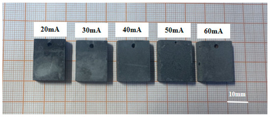
Figure 1.
Macroscopic morphology of tungsten coatings at different DC current densities.
The surface microstructure of the tungsten coating is primarily examined using SEM images. Figure 2 presents SEM images and EDS analysis diagrams of the surface microstructure of tungsten coatings produced at various current densities under direct current. The images reveal that tungsten grains are in a polygonal, agglomerated state and are relatively evenly distributed, with some sparse and irregular pores. At a current density of 20 mA/cm2, the deposition rate is slow, and tungsten nuclei have not fully developed on the substrate surface. As the current density rises to 30 mA/cm2, tungsten grain nucleation occurs concurrently, and some nuclei begin to grow gradually, leading to a few areas of grain aggregation. EDS analysis indicates that the coatings produced at current densities of 20 mA/cm2 and 30 mA/cm2 are primarily composed of pure tungsten, though there are still some uncovered substrate areas, characterized by copper. When the current density further increases to 40 mA/cm2, the higher current density hastens the nucleation process and also promotes rapid growth in some grains. Previously nucleated sites preferentially grow into larger grains, causing the coating to exhibit unevenness, yet the macroscopic surface remains relatively flat. EDS analysis confirms that the coating surface is pure tungsten, and the substrate is entirely covered. Upon reaching current densities of 50 mA/cm2 and 60 mA/cm2, the abnormal growth of grains and agglomeration become pronounced. It is because the current densities of 50 and 60 mA/cm2 have reached or exceeded the limit diffusion current density for this system, resulting in a sharp decrease in the concentration of tungsten ions at the cathode solution interface. A significant ion concentration difference is generated between the interface and the solution body, causing a drastic change in the cathode potential. The extremely high overpotential causes the existing crystal nuclei to grow preferentially and rapidly, competing for the limited tungsten ions. Due to the lack of ions at the interface, it becomes very difficult to form new crystal nuclei, leading to abnormal grain growth. The electrodeposition tends to occur at the protrusions where ions can easily reach, forming agglomerations, and ultimately resulting in abnormal growth and agglomeration of the microstructure [14].
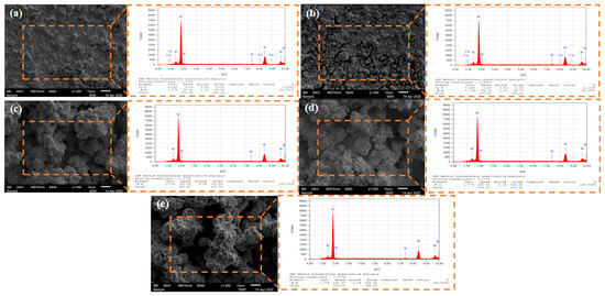
Figure 2.
SEM and EDS images of tungsten coating surface under different DC current densities: (a) 20 mA/cm2; (b) 30 mA/cm2; (c) 40 mA/cm2; (d) 50 mA/cm2; (e) 60 mA/cm2.
The evolution of the coating’s crystal structure was analyzed using an X-ray diffraction (XRD) system, which is crucial for elucidating the mechanism underlying the relationship between current density and coating integrity. Figure 3 displays the XRD spectra of the tungsten coating surface under varying direct current densities. The experimental data indicate that the XRD spectra of tungsten coatings produced at different current densities all exhibit four distinct sets of diffraction peaks. These peaks correspond to the (111), (200), (211), and (220) crystallographic planes of tungsten, confirming that the coating possesses a tungsten phase structure and exhibits good crystallinity. At current densities of 20 mA/cm2 and 30 mA/cm2, diffraction peaks corresponding to copper’s (111), (200), and (220) planes are also observed in the XRD spectra. The presence of these peaks can be explained as follows: at low current densities, the local electric field energy is insufficient to overcome the nucleation barrier, resulting in a smaller reduction in the critical nucleus size of tungsten grains [15,16]. Consequently, the nucleation rate decreases, and the growth of existing grains slows down, leading to the formation of larger grains. Local grain growth is limited, resulting in an insufficient coating thickness in those regions. Due to the substantial penetration depth of X-rays, some X-rays reach and reflect from the CuCrZr substrate, generating copper characteristic diffraction peaks. When the current density increases to 40–60 mA/cm2, both the nucleation rate and grain growth rate of tungsten significantly increase, resulting in thicker coatings. In this case, X-rays are unable to effectively penetrate the tungsten coating, thereby shielding the CuCrZr substrate signal. As a result, there are no copper diffraction peaks on the XRD patterns.
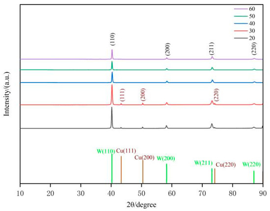
Figure 3.
XRD patterns of tungsten coatings prepared at different current densities.
3.2. Surface Morphology and Crystal Structure of Tungsten Coatings Under Pulsed Current
The characterization of the tungsten coating under specified direct current conditions shows that at a current density of 40 mA/cm2, the tungsten coating fully covers the substrate and achieves the highest deposition efficiency. However, the tungsten coating fabricated via direct current deposition exhibits pronounced abnormal grain growth, leading to a relatively rough surface. To address this issue, pulse electrodeposition was employed to improve coating quality. Figure 4 presents the macroscopic surface morphology of the tungsten coating at various pulse duty ratios. During pulse electrodeposition with a 30% duty cycle, the short conduction time results in low energy density, which leads to an uneven metallic luster on the coating surface. Nevertheless, the coating maintains good continuity, with no signs of substrate oxidation or localized exposure. As the duty cycle increases to 40%, the coating surface remains continuous and exhibits a uniform silver-white metallic luster. This improvement can be attributed to the extended current conduction time, which facilitates the uniform deposition of tungsten ions across the substrate surface, resulting in a denser coating. When the duty cycle is further increased to 50%, the prolonged conduction time leads to a thicker diffusion layer, insufficient ion replenishment, and a rougher coating surface, which causes the metallic luster to diminish.
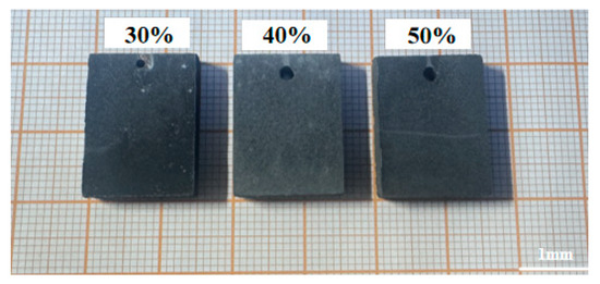
Figure 4.
Macroscopic morphology of tungsten coatings at different pulse duty cycles.
Figure 5 illustrates the microstructural features and elemental composition of the tungsten coating produced via pulsed electrodeposition at different duty cycles. The results show that the tungsten grains are densely packed, forming a polycrystalline aggregate structure characterized by irregular surfaces, pores, and protrusions. These features may be related to the characteristics of the molten salt system. At a duty cycle of 30%, the tungsten grains are relatively fine, yet the coating surface exhibits “pits”. This is attributed to the short conduction time, which results in insufficient crystal nucleus growth, leading to a mixture of dense and sparse regions and causing local non-uniformity. Increasing the duty cycle to 40% provides a moderate current conduction time, thereby extending the effective deposition period. Consequently, the ion migration and diffusion dynamics within the molten salt are significantly enhanced, promoting a higher deposition rate of tungsten ions and facilitating the relatively uniform growth of crystal grains. When the duty cycle reaches 50%, noticeable accumulation and stacking of crystal grains occur, and holes begin to appear. This phenomenon arises because a higher duty cycle corresponds to a longer current conduction time. During this stage, the continuous depletion of tungsten ions at the cathode surface leads to a sharp decrease in ion concentration near the electrode. The insufficient ion replenishment, combined with the enhanced electric field around cathode surface protrusions, promotes preferential ion deposition, resulting in dendritic growth. In contrast, the depressed areas experience slower deposition due to ion depletion, leading to the formation of holes. The resulting loose crystal structure contributes to a decline in coating performance. Energy-dispersive spectroscopy (EDS) analysis confirms that under all tested duty cycles, the coating consists of single-phase metallic tungsten with high coverage. Therefore, compared to direct current electrodeposition, pulsed electrodeposition improves deposition efficiency and effectively addresses the issue of inadequate coating coverage associated with direct current methods.
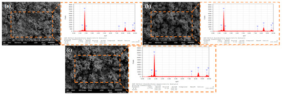
Figure 5.
SEM and EDS images of tungsten coating surface under different pulse duty cycles: (a) 30%; (b) 40%; (c) 50%.
Figure 6 presents the X-ray diffraction (XRD) spectra of tungsten coatings produced under various duty cycles. The XRD results indicate that all samples exhibit the characteristic diffraction peaks of a body-centered cubic (BCC) tungsten lattice. The main diffraction peaks are located at 2θ = 40°, corresponding to the (110) crystal plane; at 2θ = 58°, corresponding to the (200) plane; at 2θ = 73°, corresponding to the (211) plane; and at 2θ = 87°, corresponding to the (220) plane. Notably, the (110) diffraction peak is significantly more intense than the others, and its full width at half maximum (FWHM) is narrower, indicating that the tungsten coating possesses a high degree of crystallinity and a low defect density along the (110) plane during the pulsed electroplating process. The favorable lattice alignment of the (110) plane with the ion migration direction in the molten salt system synergistically promotes preferential grain growth, while the relatively low surface energy of the (110) plane facilitates nucleation. When the duty cycle increases from 30% to 40%, the conduction time of the pulse current is appropriately prolonged. Near the cathode, the metal ions are rapidly consumed due to the reduction reaction, resulting in a sudden drop in local ion concentration. The appropriate prolongation of the conduction time ensures that the ion concentration is restored in time, allowing the thermodynamically most stable (110) crystal plane to grow preferentially. This is manifested in the XRD spectrum as an increase in the relative intensity of the W(110) diffraction peak. When the duty cycle increases from 40% to 50%, the high duty cycle means a longer conduction time and a higher average current density, resulting in a significant acceleration of the deposition rate. This causes the reaction ions at the cathode interface to be rapidly consumed, while the ions in the bulk solution have no time to diffuse and replenish. In this non-equilibrium state, the deposition process no longer prioritizes the crystal plane with the lowest surface energy but rather those with the fastest growth rate, leading to a weakening of the relative intensity of the W(110) peak [17].
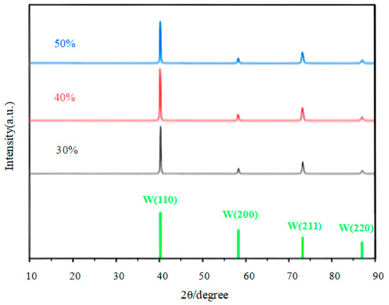
Figure 6.
XRD patterns of tungsten coatings prepared at different pulse duty cycles.
3.3. The Microstructure, Crystal Structure, and Properties of the Tungsten Coating Obtained Through Long-Term (60-h) Electrodeposition
The previous study primarily investigated the effects of two key parameters—current density and duty cycle-on the morphology and structure of tungsten coatings. It was found that under conditions of 40 mA/cm2 current density and 40% duty cycle, pure metallic single-phase tungsten coating with favorable microstructural morphology and uniform coverage could be obtained. Under these optimized conditions, a tungsten coating was fabricated through long-term electrodeposition at 943 K over a period of 60 h.
Figure 7 presents the SEM and EDS images of the surface of the long-term electrodeposited tungsten coating. The surface exhibits protrusions, with an average grain size of approximately 3 µm, which is smaller than that of tungsten coatings produced within oxide-based systems. This grain refinement is attributed to the relatively limited tungsten source and the reduced energy input due to the lower deposition temperature. The figure also reveals defect characteristics of the long-term electrodeposited tungsten coating, such as grain aggregation and pore formation. In the second picture of Figure 7, the area circled by the circle represents the grain aggregation, and the area marked by the triangle represents the pores. The non-uniform grain growth is associated with uneven nucleation of tungsten grains. Over time, the initial nucleation sites consumed a significant portion of the tungsten source, leading to rapid grain growth, whereas regions without early nucleation experienced insufficient tungsten replenishment, ultimately resulting in localized grain aggregation and inhomogeneous growth. EDS analysis confirms that the coating consists of pure tungsten, and the substrate is fully covered without detectable impurities. In addition, after a long period of electro-deposition, the anode may experience passivation or uneven dissolution, which will result in uneven current distribution, local deposition interruption, and thus form defects.
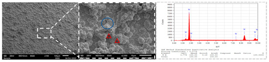
Figure 7.
SEM and EDS images of the tungsten coating surface obtained via long-term electrodeposition.
Figure 8 shows the SEM and EDS images of the cross-section of the tungsten coating after 60 h of electro-deposition. From the SEM image of the cross-section, it can be seen that after 60 h of electro-deposition, the coating thickness is 30–50 µm. Through EDS analysis, it was found that the entire cross-section consists only of the base material and the tungsten coating, with no other impurities mixed in.
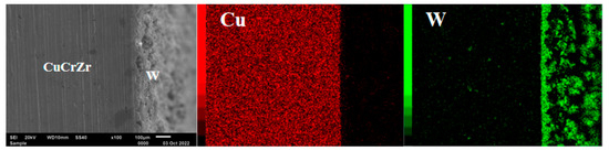
Figure 8.
SEM and EDS images of the cross-section of the tungsten coating after 60 h of electro-deposition.
Figure 9 presents the XRD pattern of the coating surface after 60 h of electrodeposition, confirming the formation of pure metallic tungsten. Texture coefficients were calculated from the XRD data and are summarized in Table 4. The results indicate that with increasing electrodeposition time, tungsten crystals exhibit relatively uniform growth in the (110), (200), and (211) crystallographic directions, suggesting a tendency toward isotropic growth of the tungsten coatings.
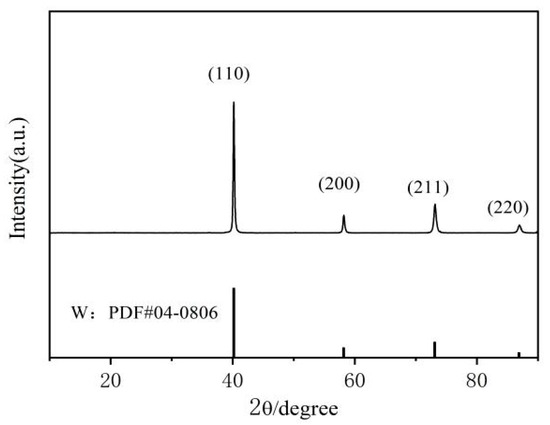
Figure 9.
XRD patterns of the tungsten coating surface after long-term (60 h) electrodeposition.
Table 4.
Grain texture coefficient of the surface of tungsten coating obtained through long-term electrodeposition.
Table 5 summarizes the physical properties of the tungsten coating fabricated via long-term electrodeposition over a 60-h period. The data show that the coating’s density of 18.60 g/cm3 is lower than the theoretical density of pure tungsten, which is 19.3 g/cm3. In addition, the coating exhibits a porosity of 2.15% and a hardness of 487.50 HV, indicating the presence of localized porosity within the coating. This phenomenon is likely attributed to the limited mass transfer efficiency of the electrolyte in the low-temperature molten salt system. However, the bonding strength of this coating is 55 MPa, which indicates that there is good interface compatibility between the substrate material and the tungsten coating. In the research on coatings on the same substrate by Li et al., they believed that when the bonding strength reached 49.28 MPa, there was good interfacial compatibility between the substrate and the coating [12].
Table 5.
Physical properties of samples with long-term electrodeposited tungsten coating.
Table 6 presents the porosity of all samples. It can be observed that after 2 h of electro-deposition, the porosity of the samples did not vary significantly, with the maximum being 1.24% and the minimum being 1.08%. However, after a long period of (60 h) electro-deposition, the porosity of the samples significantly increased to 2.15%. This is because as time progresses, smaller and more energetic grains gradually dissolve, while larger grains continue to grow to reduce the overall surface energy. Coarse grains mean fewer grain boundaries, which are the rapid filling channels for tungsten ion deposition. The structure after coarsening is more likely to contain larger pores and defects between the grains. From the roughness data in Table 6, it can be observed that the influence of current density on the surface roughness of the coating is greater than that of the power supply type. Moreover, as the electrodeposition time increases, the surface roughness of the tungsten coating significantly increases.
Table 6.
Porosity of different samples.
4. Conclusions
In this study, a KF-KCl-WO3 molten salt system was developed to reduce the electrodeposition temperature. Tungsten coatings were electro-deposited on CuCrZr substrates. Under varying the current density, current mode, duty cycle, and electrodeposition time, various tungsten coatings were produced. The microstructural and crystallographic characteristics of the coatings were systematically analyzed. Additionally, the density, porosity, and hardness of the tungsten coating deposited under relatively optimal conditions over an extended period were evaluated. The main findings are summarized as follows:
(1) In the KCl-KF-WO3 molten salt system, a metallic tungsten coating was successfully fabricated at an electrodeposition temperature of 943 K, which is 250 K lower than the 1193 K required in the Na2WO4-WO3 molten salt system.
(2) Under direct current electrodeposition, excessively low current densities resulted in slow deposition rates and insufficient grain growth, leading to incomplete coverage of the substrate. In contrast, high current densities accelerated grain nucleation but also induced abnormal growth of pre-existing grains, increasing surface roughness. Transitioning from direct current to pulse current electrodeposition improved ion migration and diffusion within the molten salt. An appropriate duty cycle further enhanced the deposition rate. Consequently, the optimal electrodeposition parameters in this system were determined to be an electrodeposition temperature of 943 K, a current density of 40 mA/cm2, pulse current mode, and a duty cycle of 40%.
(3) Using the optimized parameters in the KCl-KF-WO3 molten salt system, a tungsten coating was obtained after 60 h of long-term electrodeposition. The surface tungsten grains exhibited a fine and uniform morphology, with an average size of 2–6 µm. The coating had an average thickness of approximately 40 µm, a porosity of 2.15%, a hardness of 487.50 HV, and a bonding strength of 55 MPa.
Author Contributions
Conceptualization, X.D. and W.L.; methodology, W.L.; validation, W.L. and Y.L.; formal analysis, W.L. and Z.G.; investigation, Z.G.; resources, X.D. and W.L.; data curation, W.L.; Writing—original draft, X.D. and W.L.; writing–review & editing, W.L. and Y.L.; visualization, Z.G.; supervision, Y.Z.; project administration, Y.Z.; funding acquisition, Y.Z. All authors have read and agreed to the published version of the manuscript.
Funding
This study was supported by National MCF Energy R&D Program (NO. 2019YFE03130002).
Institutional Review Board Statement
Not applicable.
Informed Consent Statement
Not applicable.
Data Availability Statement
Data are contained within the article.
Conflicts of Interest
The authors declare no conflicts of interest.
References
- Ongena, J.; Koch, R.; Wolf, R.; Zohm, H. Magnetic-confinement fusion. Nat. Phys. 2016, 12, 398–410. [Google Scholar] [CrossRef]
- Matthews, G.F.; Coad, P.; Greuner, H.; Hill, M.; Hitai, T.; Likonen, J. Development of divertor tungsten coatings for the JET ITER-like wall. J. Nucl. Mater. 2009, 390–391, 934–937. [Google Scholar] [CrossRef]
- Piip, K.; Paris, P.; Hakola, A. Influence of He/D2 Plasma Fluxes on the Morphology and Crystallinity of Tungsten Coatings. Phys. Scr. 2014, 89, 39–50. [Google Scholar] [CrossRef]
- Ribis, J.; Bordas, E.; Trocellier, P. Comparison of the neutron and ion irradiation response of nano-oxides in oxide dispersion strengthened materials. J. Mater. Res. 2015, 30, 2210–2221. [Google Scholar] [CrossRef]
- Sun, Q.L.; Mao, X.C.; Yao, Y.F.; Li, J.N.; Shen, Z.S.; Tu, K.N.; Liu, Y.X. Effect of WC thickness on the microstructure and properties of WC-C/DLC coated 304 steel. J. Appl. Surf. Sci. 2025, 704, 163418. [Google Scholar] [CrossRef]
- Xie, J.J.; Fang, H.J.; Wang, Y.X.; Wang, W.Q.; Yu, J.H.; Li, J.C.; He, X.D.; Pu, J.B. Controlling the porosity to enhance the high-temperature tribological performance of plasma-sprayed NiCr–Cr3C2-BaF2/CaF2 coating by adopting axial feeding. J. Mater. Res. Technol. 2025, 36, 2577–2588. [Google Scholar] [CrossRef]
- Ganne, T.; Crépin, J.; Serror, S.; Zaoui, A. Cracking behaviour of PVD tungsten coatings deposited on steel substrates. Acta Mater. 2002, 50, 4149–4163. [Google Scholar] [CrossRef]
- Liu, Y.H.; Zhang, Y.C.; Li, H.L.; Liu, D.J. Analysis on Composition of Binary Molten Salt Na2WO4-WO3 and Study of Electrodepositing Tungsten Coatings. J. Mater. Her. 2015, 29, 34–36+45. [Google Scholar] [CrossRef]
- Jiang, F.; Zhang, Y.C.; Li, X.L.; Sun, N.B.; Wang, L.L. Tungsten coating prepared on V-4Cr-4Ti alloy substrate by electrodeposition from molten salt in air atmosphere. Fusion Eng. Des. 2014, 89, 83–87. [Google Scholar] [CrossRef]
- Sun, N.B.; Zhang, Y.C.; Lang, S.T.; Jiang, F.; Wang, L.L. Tungsten coatings electro-deposited on CFC substrates from oxide molten salt. J. Nucl. Mater. 2014, 455, 450–453. [Google Scholar] [CrossRef]
- Li, Y.S.; Dong, X.X.; Liu, Q.; You, Y.J.; Gao, Z.Y.; Zhang, Y.C. Preparation and Properties of Thick Tungsten Coating Electrodeposited from Na2W04-WO3-KCl-NaF Molten Salt System. J. Coat. 2024, 14, 1471. [Google Scholar] [CrossRef]
- Qi, Y.F.; Tang, Y.H.; Wang, B.; Zhang, M.; Ren, X.Q.; Li, Y.G.; Ma, Y.T. Characteristics of tungsten coatings deposited by molten salt electrodeposition and thermal fatigue properties of electrodeposited tungsten coatings. Int. J. Refract. Met. Hard Mater. 2019, 81, 183–188. [Google Scholar] [CrossRef]
- Nohira, T.; Ide, T.; Meng, X.D.; Norikawa, Y.; Yasuda, K. Electrodeposition of Tungsten from Molten KF-KCl-WO3 and CsF-CsClWO3. J. Electrochem. Soc. 2021, 168, 046505. [Google Scholar] [CrossRef]
- Zhu, D.; Zhang, W.F.; Lei, W.N. Study on Refinig Grains of Nanocrystalline Materials Based on Electrodeposition. J. Synth. Cryst. 2021, 5, 765–769. [Google Scholar] [CrossRef]
- Pérez, H.D.; González, A.J.; Romo, R.M.; Hernández, R.S.; Mejía, E.A.; Gil, M.P.; Piñon, S.N.; Garrido, S.A.; Pardavé, P.M. Electrochemical Nucleation and Growth of Neodymium on Glassy Carbon Electrodes using Reline as a Deep Eutectic Solvent. J. Electrochim. Acta 2025, 535, 146643. [Google Scholar] [CrossRef]
- Wang, R.Q.; Li, G.Y.; Wu, F.; Wang, S.M.; Zhang, C.Z. Cycling performance of Li metal anode in localized high concentration electrolyte and dynamic mechanism analysis. J. Electroanal. Chem. 2024, 959, 118176. [Google Scholar] [CrossRef]
- Chen, W.T.; Wang, Q.W.; Yang, Y.F. Research on Parameter Regulation and Structural Properties of Pulse Electrodeposited Zn-Ni-PTFE Composite Coatings. J. Surf. Eng. Remanuf. 2025, 25, 1–18. [Google Scholar] [CrossRef]
Disclaimer/Publisher’s Note: The statements, opinions and data contained in all publications are solely those of the individual author(s) and contributor(s) and not of MDPI and/or the editor(s). MDPI and/or the editor(s) disclaim responsibility for any injury to people or property resulting from any ideas, methods, instructions or products referred to in the content. |
© 2025 by the authors. Licensee MDPI, Basel, Switzerland. This article is an open access article distributed under the terms and conditions of the Creative Commons Attribution (CC BY) license (https://creativecommons.org/licenses/by/4.0/).