Article

Silicon Oxycarbide Coatings Produced by Remote Hydrogen Plasma CVD Process from Cyclic Tetramethylcyclotetrasiloxane

by
Agnieszka Walkiewicz-Pietrzykowska
1,*,
Krzysztof Jankowski
2,
Romuald Brzozowski
1,
Joanna Zakrzewska
1 and
Paweł Uznański
1,*
1
Centre of Molecular and Macromolecular Studies, Polish Academy of Sciences, Sienkiewicza 112, 90-363 Lodz, Poland
2
Technical Department, Jacob of Paradies University, Chopina 52, 66-400 Gorzow Wielkopolski, Poland
*
Authors to whom correspondence should be addressed.
Coatings 2025, 15(10), 1179; https://doi.org/10.3390/coatings15101179
Submission received: 27 August 2025 / Revised: 1 October 2025 / Accepted: 2 October 2025 / Published: 8 October 2025

Abstract

The development of high-speed computers and electronic memories, high-frequency communication networks, electroluminescent and photovoltaic devices, flexible displays, and more requires new materials with unique properties, such as a low dielectric constant, an adjustable refractive index, high hardness, thermal resistance, and processability. SiOC coatings possess a number of desirable properties required by modern technologies, including good heat and UV resistance, transparency, high electrical insulation, flexibility, and solubility in commonly used organic solvents. Chemical vapor deposition (CVD) is a very useful and convenient method to produce this type of layer. In this article we present the results of studies on SiOC coatings obtained from tetramethylcyclotetrasiloxane in a remote hydrogen plasma CVD process. The elemental composition (XPS, EDS) and chemical structure (FTIR and NMR spectroscopy-13C, 29Si) of the obtained coatings were investigated. Photoluminescence analyses and ellipsometric and thermogravimetric measurements were also performed. The surface morphology was characterized using AFM and SEM. The obtained results allowed us to propose a mechanism for the initiation and growth of the SiOC layer.

1. Introduction

The development of high-speed computers and electronic memories, high-frequency communication networks, electroluminescent and photovoltaic devices, flexible displays, and so on requires new polymer materials with unique properties, such as a low dielectric constant, a tunable refractive index, high hardness, thermal resistance, and processability [1,2,3,4,5]. These materials will be primarily used for the production of thin, functional layers or coatings. Polysiloxanes have a number of desirable properties required in modern technologies such as a low dielectric constant [6,7,8,9], high thermal and chemical stability, and good mechanical properties [10,11]. They are mainly used in electronics as a dielectric material in integrated circuits and memories, in photovoltaics for the production of solar cells as protective and passive layers, in lithium-ion cells as a ceramic anode material, and as a composite nanomaterial in supercapacitors [12]. Furthermore, due to the possibility of surface functionalization, SiOC layers are used in biomedicine as a material for biocompatible coatings and sensors [13,14,15]. Unfortunately, linear, functional polydimethylsiloxanes do not form stable layers. To obtain functionalized siloxanes with a well-defined structure as precursors to thin films, it is necessary to develop new synthetic methods enabling their crosslinking. Such a method is the controlled synthesis of organosilicon polymers and copolymers using the hydride transfer process (HTP) in siloxanes with a Si-H functional group, recently discovered at ours laboratory [16]. An example of a siloxane precursor undergoing HTP and potentially useful for the production of advanced coatings is 1,3,5,7-tetramethylcyclotetrasiloxane (D4H). In this case, the reaction proceeds in an unusual manner, leading to the formation of branches accompanied by extensive cyclization, leading to the formation of a siloxane polymer structure functionalized with Si–H groups and ultimately to a cross-linked and insoluble polymer of the SiOC-type layer. Another method of crosslinking and curing hydrogen silanes is to use hydrogen radicals.
Based on previous studies conducted at our facility with linear hydrosilyl monomers [17,18], we expected that the use of cyclic siloxane precursors (such as D4H) and a selective CVD process initiated by atomic hydrogen would allow obtaining good quality SiOC layers.
In the RHP-CVD (Remote Hydrogen Plasma Chemical Vapor Deposition) process, the layer-forming reactions occur outside the plasma region, where only non-energetic, long-lived hydrogen radicals are present. Hydrogen atoms attack only the hydrogen silane Si–H groups in the precursor. The activated precursor molecules serve as reactive fragments or reactive sites in the polymerization, branching, and cross-linking processes. The remote CVD process leads to high uniformity of the chemical structure and morphology of the deposited layer. The main factor controlling the deposition reactions, in addition to the physical parameters of the plasma, is the temperature of the substrate (TS) on which the layer deposition and growth occur. Temperature influences the properties of the deposit, which can change from a highly cross-linked polymer structure to a ceramic structure during the CVD process.
RHP-CVD reactions using siloxanes demonstrate new possibilities for the synthesis of silicon oxycarbide coatings, which are crucial for the production of new materials. Cyclic hydrosiloxane layers may be particularly useful for obtaining dielectrics with a low dielectric constant (low k value), essential in the production of modern electronic systems.
The key to innovation in SiOC research is currently shifting from “mass” production to precise “material design” at the molecular level. This allows the creation of advanced layers with unique, often multifunctional properties, opening the door to applications in the most demanding fields of science and technology. Our research is a key part of this trend, and the method we employ enables the “design” of materials with specific, predetermined properties. In this paper we presented the preparation and characterization of SiOC thin films, a class with a given composition and properties from a new organosilicon precursor: cyclic tetramethylcyclotetrasiloxane (D4H).

2. Materials and Methods

Thin films were deposited using the commercially available cyclic precursor 1,3,5,7-tetramethylcyclotetrasiloxane ((HMeSiO)4, D4H) (Thermoscientific, Waltham, MA, USA 99%). The linear analog of D4H is 1,1,3,3-tetramethyldisiloxane (TMDSO), which possesses Si–O and Si–CH3 structural units, which are the source of the atoms in the produced film, and reactive Si–H hydrosilyl units. Their presence, as demonstrated in previous work by our group [19], is necessary to initiate the selective CVD process using remote hydrogen plasma.
SiOC thin films from the D4H precursor were deposited in the microwave-assisted CVD reactor as previously described in detail [20]. Briefly, the system consists of three sections: a glass tube, the upper part of which is coupled to microwaves (2.45 GHz) and is used to generate atomic hydrogen. The lower part is a remote section and is equipped with a Wood’s horn photon trap. The tube is connected to a CVD reactor through a center conical joint (29/32). A CVD reactor consists of two flat flange lids (HWS Labortechnik, Mainz, Germany) with nominal widths of 20 cm, also having side sockets, sealed with an O-ring. A heated stainless-steel substrate holder (13 cm in diameter) was placed in the lower lids. A source compound injector (4 mm in diameter) is located at the inlet of the hydrogen stream approximately 4 cm in front of the substrate. The distance between the plasma edge and the substrate was ~40 cm. No deposition was observed during CVD process in the remote section, indicating that there was no back diffusion of a source compound into the hydrogen supply tube.
The D4H monomer is easy to dose in vapor form using the Mass Flow Controller (MKS, Herdecke, Germany) (MFC). Despite the high boiling point of the compound (b.p. = 135 °C) and the heat of evaporation of ΔHvap: 177.9 kJ/mol (42.5 kcal/mol), no temperature control of the monomer supply line to the CVD reactor was required.
The CVD reactor was evacuated using a two-stage rotary pump (40 m3 h−1, Leybold, Model TRIVAC D40B). The chamber pressure was measured with a resistive manometer (Pfeiffer Vacuum, Model TPR 280, Wetzlar, Germany) and monitored via a TPG 262 unit. The samples were deposited with the following parameters: hydrogen gas flow rate F(H2) = 100 sccm, monomer flow rate F(D4H) = 5 sccm (5.2 mg min−1), total pressure during deposition p = 380 Pa (2.85 Torr), and input power of 2.45 GHz microwave plasma p = 70 W. The hydrogen flow was regulated by a mass flow controller (MKS, Herdecke, Germany). The coatings were produced in the substrate temperature range TS = 30–350 °C on p-type c-Si (100) wafers for the infrared, XPS, ellipsometric analysis, and nanoindentation tests and on Fisher microscope glass (20 × 20 × 0.2 mm) for the film mass determination.
Fourier transform infrared (FTIR) absorption spectra of the coatings were measured in normal transmission mode using a JASCO FTIR-6200 (Tokyo, Japan) spectrometer with a nitrogen purge.
The chemical structure of the samples was investigated by 29Si and 13C solid-state CP/MAS NMR measurements with proton decoupling using a Bruker Model Avance III WB 400 MHz NMR spectrometer (Billerica, MA, USA) at a frequency of 79.5 and 100.6 MHz for 29Si and 13C nuclei, respectively. CP cross polarization contact time was 10 ms for both 1H−29Si and 1H−13C CP/MAS NMR experiments. The sample rotation frequency was 8 kHz. Spectra were collected a few days after deposition. The films measured by CP/MAS NMR were deposited on an unheated silicon wafer substrate for about 300 min. The resulting material (approx. 200 mg) was then scraped off and analyzed.
Surface chemical characterization of the SiOC films was carried out using AXIS Ultra photoelectron spectrometer (XPS, Kratos Analytical Ltd., Manchester, UK) equipped with a monochromatic Al–Kα X-ray source (1486.6 eV). The power of the anode was set at 150 W, and the hemispherical electron energy analyzer was operated at a pass energy of 20 eV for all high-resolution measurements. Measurements were carried out with a charge neutralizer. The main component of the C 1s line, assigned to C–C/C–H and set to 284.6 eV, was used to calibrate the spectra.
The surface morphology of the films was studied by atomic force microscopy (AFM) on c-Si substrates using a Nanoscope IIIa Digital Instruments (Veeco, Santa Barbara, CA, USA) equipped with a JV scanner operating in tapping mode (Veeco, Santa Barbara, CA, USA). The surface roughness was characterized by the root mean square Rrms of the laser beam position, which is equal to the statistical deviation of the vertical displacement component of the blade.
Photoluminescence (PL) spectra were recorded at room temperature by means of a Horiba Jobin Yvon, Fluorolog 3–22 spectrofluorimeter (Oberursel, Germany) using an excitation wavelength of 350 nm.
SEM images were obtained using Jeol 6010LA (Tokyo, Japan) at an accelerating voltage of 10 kV, connected to a secondary electron detector and X-ray energy dispersive spectrometer (EDS). The samples were placed on a double-sided conductive tape on an aluminum holder. Several images were obtained from various parts of the sample, to assure the reproducibility of the final image taken as representative of the entire sample, as well as the silica EDS elemental analysis.
Thickness and optical properties of the coatings deposited on the c-Si wafers were obtained using variable-angle spectroscopic ellipsometry (VASE) with a J. A. Woollam V-VASE ellipsometer (Lincoln, IL, USA). The ellipsometric angles psi (Ψ) and delta (Δ) were measured in the range of 260–1000 nm with a step of 5 nm, at three incidence angles of 65°, 70°, and 75°, at 20 revolutions of the analyzer to average each measured point signal for all samples. To obtain the values of thickness and optical parameters n (λ) and k (λ), i.e., the refractive index (RI) and extinction coefficient, respectively, the Cauchy–Urbach dispersion equation was used as a model for fitting to ellipsometric data. The film density was calculated based on independently determined mass and thickness values measured gravimetrically and ellipsometrically, respectively.
Thermogravimetric measurements of the changes in the SiOC deposit mass as a function of temperature were performed using a TGA 5500 device (TA Instruments, New Castle, DE, USA) in the range of 30–1000 °C, at a heating rate of 10 °C/min in nitrogen flow. Thermal analysis of the samples was performed by differential scanning calorimetry (DSC) by heating them from −50 °C to 350 °C at a rate of 10 °C/min using a DSC 2920 calorimeter (TA Instruments, New Castle, DE, USA).

3. Results and Discussion

3.1. Influence of Substrate Temperature on Deposition Kinetics

The rate of growth of the rd layer and the efficiency of the CVD process for the D4H precursor depended on the substrate temperature (Figure 1a). With the increase in substrate temperature, the deposition rate decreases from the maximum value of about rd = 16.3 nm∙min−1 at room temperature of the substrate, and above 200 °C, it is set at 2.1 nm∙min−1 for TS = 350 °C. Figure 1b shows the activation dependence of the growth rate as a function of the reciprocal of temperature.
On the Arrhenius diagram, as in the case of the three previously discussed precursors, two linear relationships can be distinguished, related to two stages of layer growth in the range up to 180–190 °C and above 200 °C, which correspond to layers with different degrees of hydrogenation and cross-linking—polymer-like and ceramic-like (see IR studies). The calculated negative activation energies of Eapp. = 0 kJ∙mol−1 and Eapp. = −11.5 kJ∙mol−1, respectively, indicate that the CVD process is controlled mainly by adsorption of vapor-phase layering precursors on the growth surface. The apparent activation energy resulting from the Arrhenius equation, Eapp., can be described by the equation:
E a p p . = E a + Δ H a d
where Ea is the activation energy of the layer-forming reaction, and ΔHad is the apparent heat of adsorption of the layer precursors on the growth surface, which has a negative value. The negative value of Eapp. calculated from the graph is due to the fact that the absolute value Δ of Had is greater than the value of Ea.

3.2. Chemical Structure of CVD Layers

The chemical structure of CVD layers with D4H that were deposited on silicon wafers was studied using transmission infrared absorption spectroscopy (FTIR) and X-ray photoelectron spectroscopy (XPS).

3.2.1. FTIR Analysis of Layer Structure

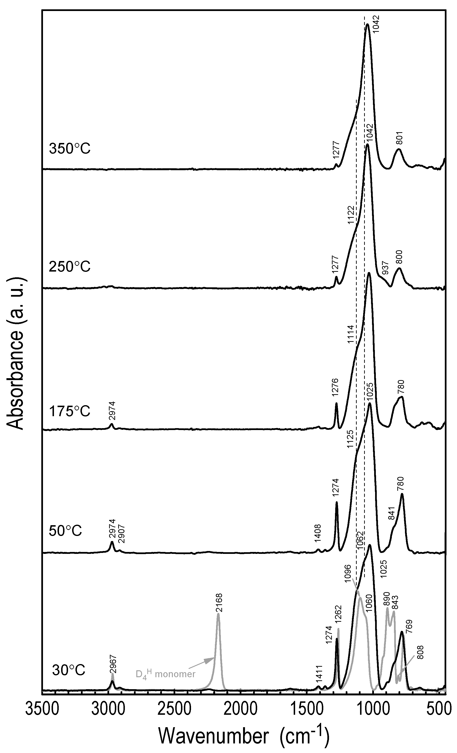
Figure 2 shows the transmission FTIR spectra of D4H layers obtained at different substrate temperatures. The assignment of IR bands to individual groupings is presented in Table 1. The spectra show that the temperature of the substrate has a strong influence on the chemical structure of the layers, similarly to CVD layers obtained from other monomers [21]. These layers are amorphous hydrogenated structures of silicon, oxygen, and carbon, which, with increasing temperature, take on the structure of silicon oxycarbide, SiOC, of a ceramic character.
The conditions of the process have been selected in such a way that during deposition on an unheated substrate in the layer, products containing the reactive silyl moiety Si–H at 2168 cm−1 and 918 cm−1, which are present in the monomer molecule, are not observed. The rapid disappearance of Si–H bonds proves the efficient reaction of the Si–H moiety with atomic hydrogen, leading to the formation of layering products. There is also a complete chemical reorganization of the O–SiH(CH3) group, manifested by a change in the position of the vibration band δas(CH3) from 1262 cm−1 to 1274 cm−1 and the disappearance of the complex band from the maximum at 890 cm−1. The increase in substrate temperature causes the gradual disappearance of absorption bands from tensile vibrations of C–H (2967–2907 cm−1) and methylsilyl groups, Si–Mex (1274 cm−1), and the formation of wide bands with maxima in the range of 1200–900 cm−1 and 900–700 cm−1, which are characteristic of the siloxane (Si–O) and carbosilane (Si–CHx) moieties and, at the highest temperature, even of inorganic carbide bonds (silicon carbide), Si–C [17,22,23,24,25,26].
Already, for the TS = 30 °C layer in relation to the precursor (Figure 2), significant changes in the position and shape of the bands can be seen in the range of 1300–680 cm−1, which result from the possibility of overlapping signals from the newly formed groups. As can be seen from the number of inflection points, the wide absorption band in the range of 1200–900 cm−1 consists of three bands with maxima at 1114, 1062, and 1025 cm−1 corresponding to the cyclic and linear bonds Si–O–Si (or Si–O–C) and the Si–CH2–Si moiety, respectively. In the 950–680 cm−1 band, in the spectra of the layers obtained at Ts = 30 °C, there are three component bands, 890 cm−1, 843 cm−1, and 780 cm−1, derived from Si–Mex and carbosilane Si–CH2–Si moieties, respectively.
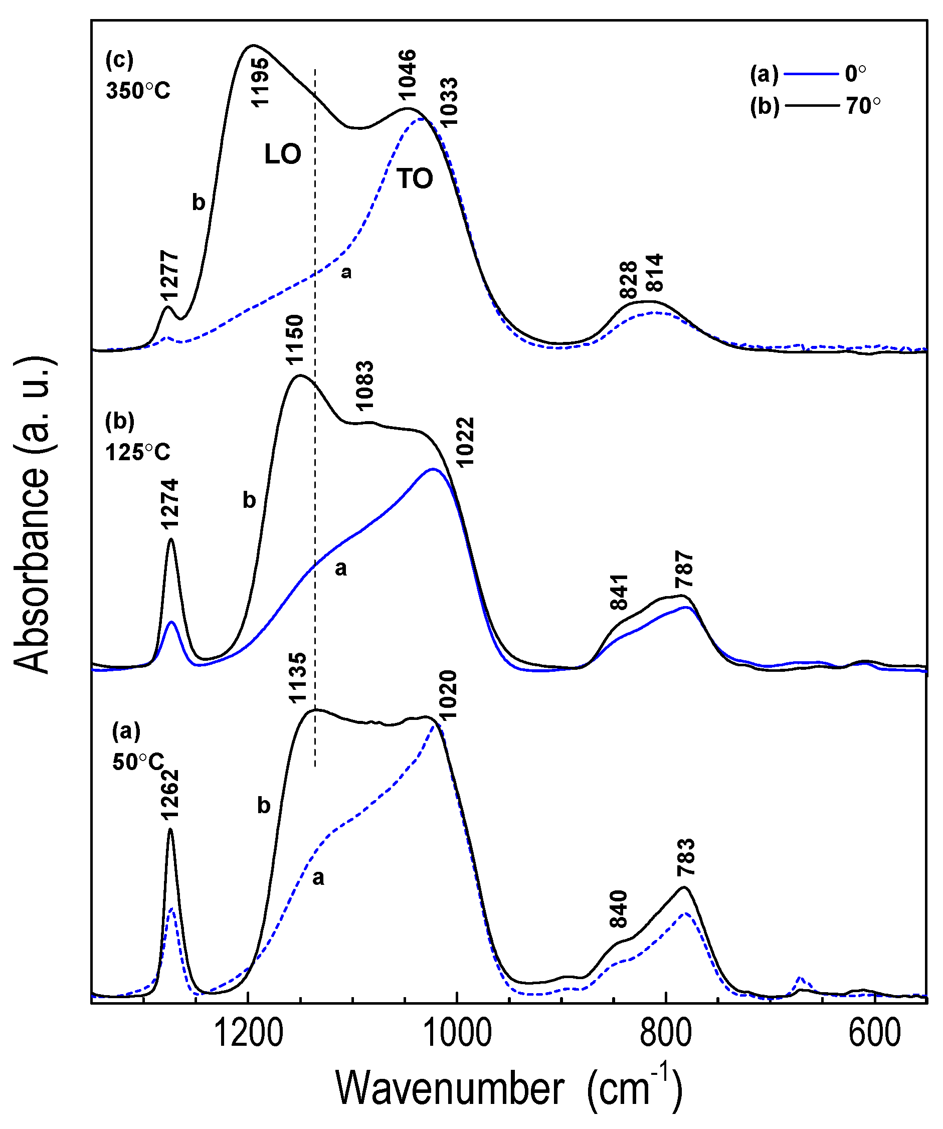
The presence of temperature-initiated cross-linking processes during the deposition of CVD layers from D4H can be demonstrated and characterized by infrared transmittance measurements, analogous to the description of an amorphous SiO2 silica web, in which there are collective vibrations of atoms—longitudinal (LO) or transverse (TO) phonons in relation to wave propagation (Figure 3). Cross-linked ceramic layers should differ spectrally from polymer layers. Figure 3 shows the IR spectra of the layers produced at 50 °C (D4H-CVD-50 °C), 125 °C (D4H-CVD-125 °C), and 350 °C (D4H-CVD-350 °C), which were taken at two angles of incidence of the analysis beam θ = 0° and 70° relative to the normal beam. The spectrum of the sample TS = 50° in the range of 1200–900 cm−1 for θ = 70° differs significantly from the spectrum made for θ = 0° by the developed maximum at 1135 cm−1, which in the normal spectrum has the character of an extensive ridge. As the temperature increases, this band increases in intensity, shifting slightly towards higher energy. It turns out, however, that for TS = 350 °C, we observe two bands in the spectrum—the one developed in TS = 125 °C at 1150 cm−1 and the new ones with a maximum at 1195 cm−1. The 800 cm−1 band is also modified by the appearance of a ridge on the higher energy side at 828 cm−1. Thus, the bands associated with the Si–O–Si, Si–C and Si–O–C vibrations clearly depend on the slope of the sample. The interpretation of these changes should be associated with the vibrations of the formed silica/silicon oxycarbide network [27].
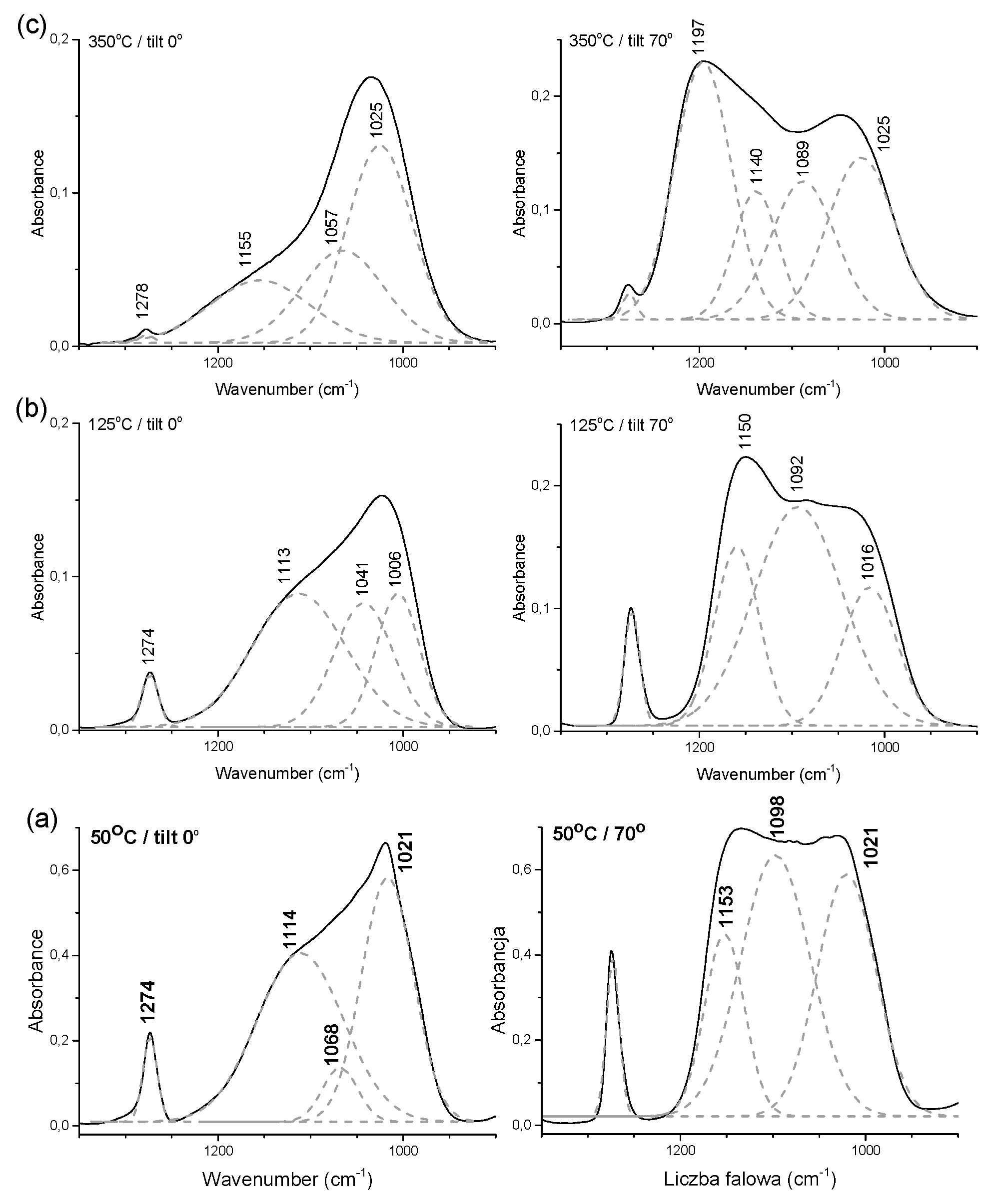
The nature of the changes in the IR spectra as a function of the temperature TS was further analyzed in detail by means of spectral distribution into Gaussian component bands (Figure 4). The case in the range of 1250–900 cm−1 consists of three bands, at 1021, 1041, and 1113 cm−1, for spectra recorded at normal inclination (θ = 0°), and at 1021, 1098, 1153 cm−1, for measurements at an angle of θ = 70°, for all overlapping temperatures TS. A new band at 1197 cm−1 appeared for TS = 350 °C at an angle of inclination of θ = 70°.
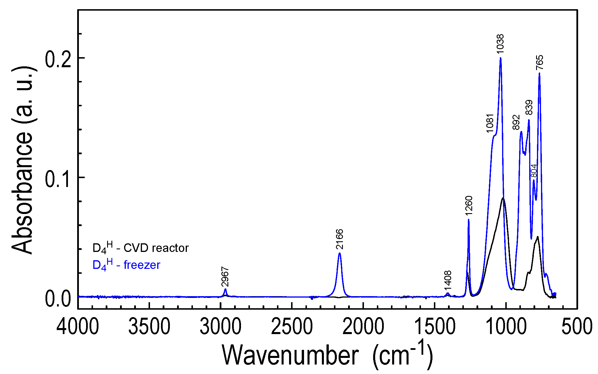
Volatile products obtained in the CVD process and frozen in a cold trap at the liquid nitrogen temperature (D4H-Freezer) were also tested by FTIR-ATR (Figure 5). Comparing this powder material with samples deposited in a CVD reactor at 30 °C (D4H-CVD-30 °C), its structure is similar, as can be seen from the analysis of IR spectra, to the structure of the monomer.

3.2.2. Chemical Composition Analysis by XPS

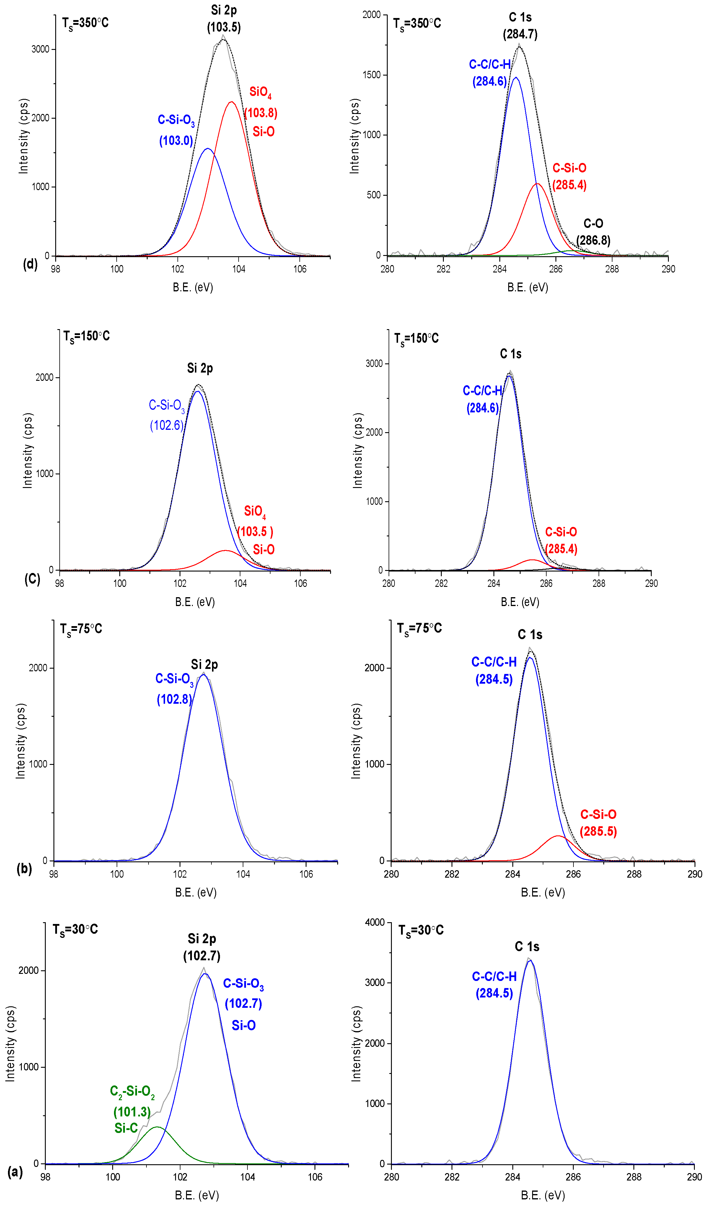
In the photoelectron spectra of X-rays of XPS radiation made in a narrow energy scan recorded for the layers from D4H for TS substrate temperatures in the range of 30–350 °C, photoelectron bands characteristic of silicon–carbon deposits are visible, corresponding to silicon atoms Si2p and Si2s, carbon C1s, and oxygen O1s. The areas under these bands were used to calculate the atomic composition of the obtained layers.
High-resolution XPS scans (so-called detailed scans) provide information about the chemical environment of a given element as a result of slight differences in binding energy (1–10 eV). An example of the separation of individual photoelectron bands into component bands for the layers obtained from D4H at substrate temperatures TS = 30°, 75°, 125°, and 350 °C is shown in Figure 6.
Individual XPS component bands of the studied layers with D4H identified on the basis of literature data [28] are presented in Table 2.
From the data in this Table 2 it can be seen that in the Si2p band, there are components from inorganic SiC bonds (101.3 eV) and SiO bonds (102.7, 103.5, 103.8 eV). In contrast, the C1s photoelectron band contains the component bands assigned to the CHx or CC (284.5 ± 0.2 eV) and CSiO (285.4 ± 0.2 eV) moieties.
With the increase in the substrate temperature, the position of the maximum Si2p moves from the initial position of 102.7 eV to 103.5 eV for the layer obtained at 350 °C. This is accompanied by the disappearance of Si–(O2)– bonds and the formation of Si–(O3)– T-type (T type—Si structures with three adjacent oxygen atoms) moieties for intermediate TS temperatures and then Si–(O4)– (Q-type Si structures with a four adjacent oxygen atoms) structures for TS > 200. The constituent band assigned to Si–C carbide structures is not observed. In the case of the C-1s band, which for the CVD-30 °C layer comes from the organic bonds CHx/C–C, with the increase in temperature, we observe a change in its half-width caused by the appearance of a new component band associated with the C–O–Si structure. It should be noted that the absence/low intensity of the XPS band from Si–H bonds proves that these units are very reactive with atomic hydrogen and few of them, if they reach the layer, are incorporated with hydrogen abstraction. It is worth noting that the main direction of structural changes observed on the basis of the XPS analysis is consistent with the results of FTIR spectroscopy described earlier.

3.2.3. Elemental Composition of the Layers

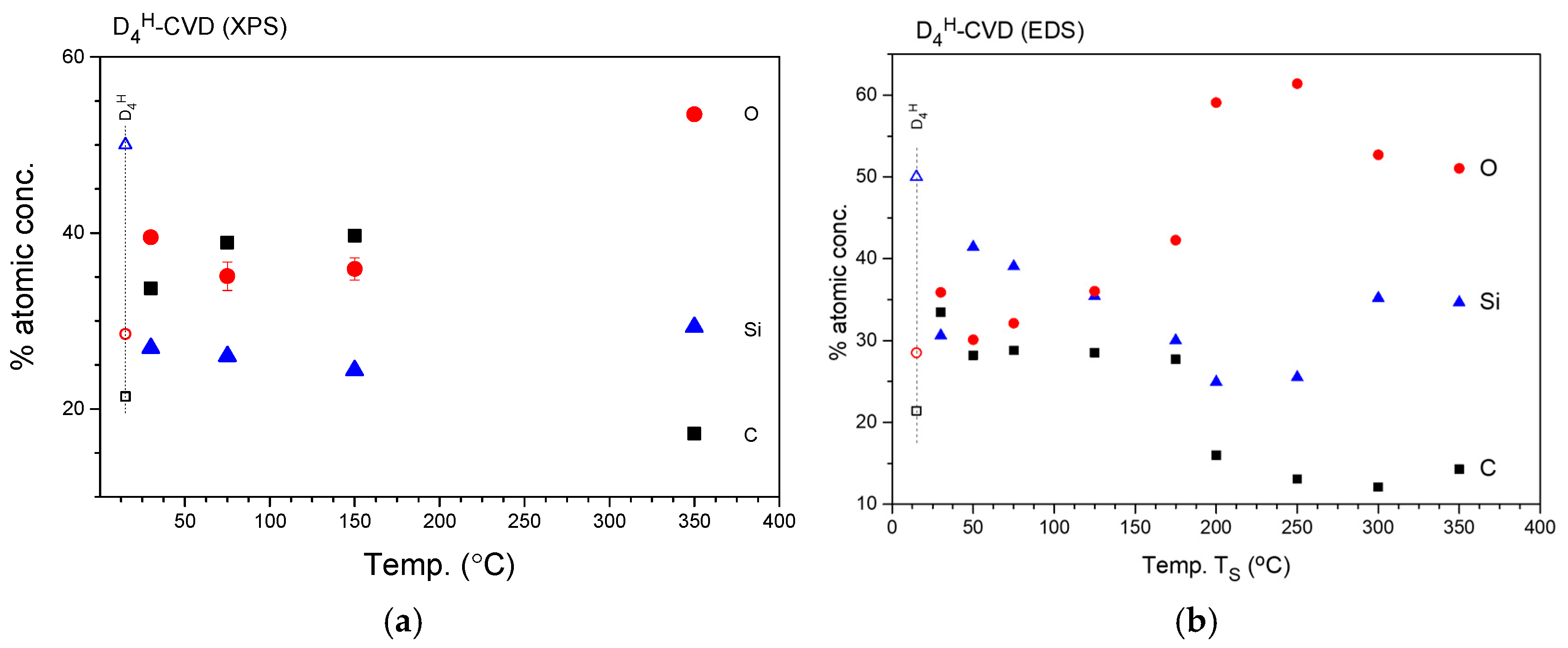
The surface atomic compositions of the films calculated from the XPS analyses together with the volume composition calculated from the EDX-SEM analysis are given on Figure 7.
The elementary composition of the surface zone of the layers was determined from the total area of the photoelectron bands Si2p, C1s, and O1s. Figure 7a shows the temperature relationships of the relative atomic fraction of individual elements on the surface of the layers obtained from D4H in the range of TS = 30–350 °C.
As can be seen from the relationship between changes in the elemental composition of the surface zone and the increase in substrate temperature, the oxygen share increases and the carbon share decreases, while the silicon content remains at a similar level (Figure 7a). Interestingly, noticeable changes in the elemental composition occur at substrate temperatures above 150 °C. A significant value of O/Si~1.8 achieved at high substrate temperatures of TS~350 °C proves that for TS > 200 °C, there is elimination of organic groups in the deposition process with simultaneous formation of mainly Si–O bonds.
Figure 7b shows the percentage atomic composition of the layer depending on the temperature of the TS substrate, which was determined by energy-dispersive X-ray spectroscopy (EDS). Literature data for various silicon carbide, silicon oxycarbide, and silicon carbonitride precursors [18] show that the atomic concentrations of individual elements in the volume of the layer are almost constant, except for the area adjacent to the substrate and the surface zone. This proves the high chemical homogeneity of the layer resulting from the defined mechanism of initiation of layer-forming products. The graph shows the changes in the relative percentage of three elements, oxygen (O), silicon (Si), and carbon (C), depending on the substrate temperature, in the range from room temperature 30 °C to 350 °C. The analysis shows that as the substrate temperature increases, the proportion of oxygen in the D4H-CVD layers increases steadily, reaching its maximum close to 60% in the temperature range from 200° to 250 °C. Silicon, on the other hand, shows the highest percentage share of 35%–40% in layers deposited at a temperature of 100 °C. In the temperature range from 100° to 250 °C, the proportion of silicon decreases significantly, but after reaching a temperature of 300 °C, it rises again and stabilizes at 35%, maintaining this level up to 350 °C. The percentage of carbon is stable in the temperature range from 50 °C to about 175 °C, remaining at about 30%. After exceeding the temperature of 200 °C, the share of carbon decreases significantly, falling below 20%. The increase in substrate temperature promotes an increase in the proportion of oxygen in the D4H-CVD layers, which may suggest an increased presence of oxides at higher temperatures. Silicon, although initially dominant at lower temperatures, exhibits complex dynamics, with a marked decrease at medium temperatures and then an increase at higher temperatures. Carbon, on the other hand, retains a relatively stable percentage share in the average temperature range, but its content decreases significantly at higher temperatures.

3.2.4. 29Si and 13C NMR Spectroscopy of D4H-CVD and D4H-Freezer Films

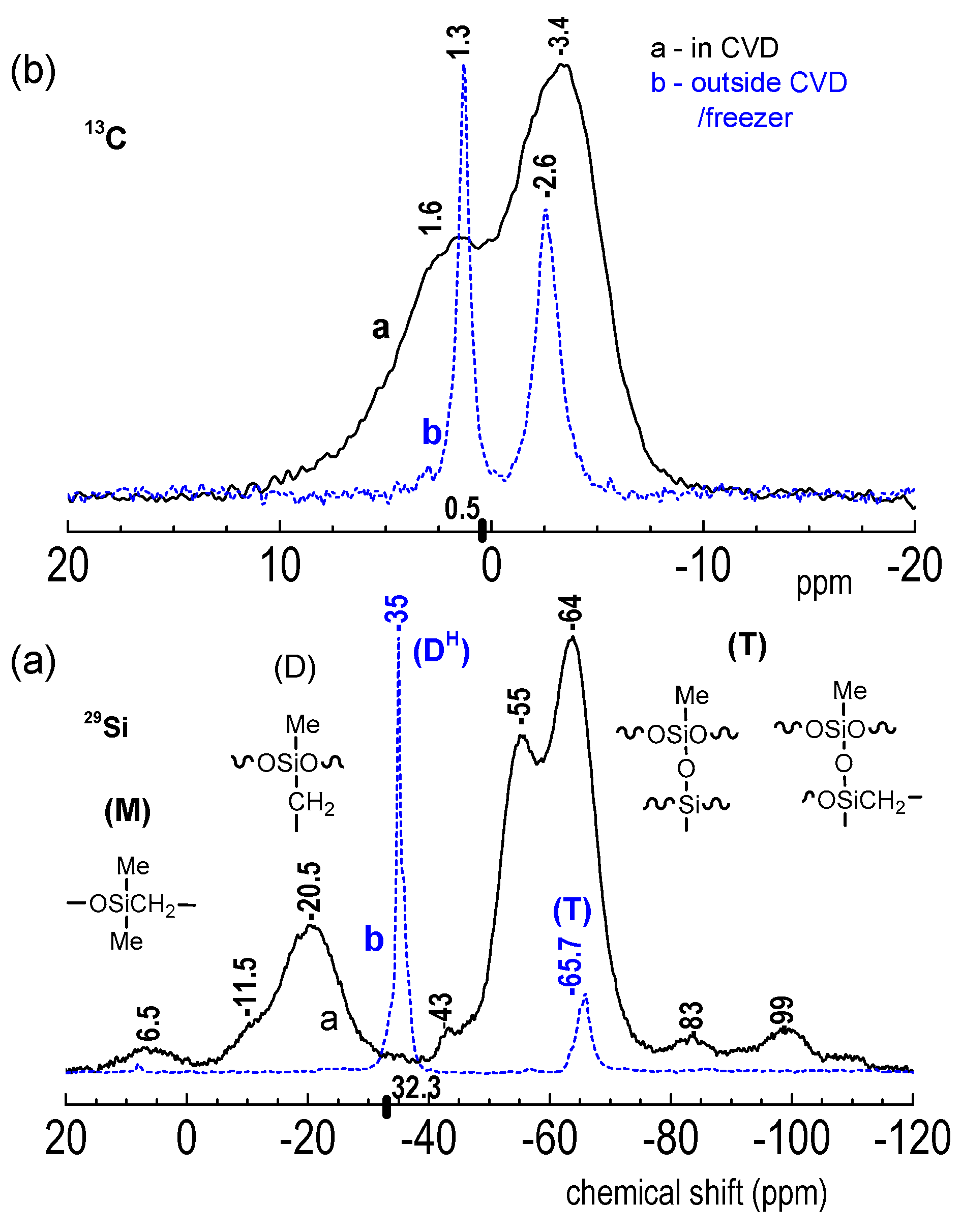
For NMR measurements, samples after a two-hour deposition were used, collected from two different locations in the system: (a) deposited in the CVD reactor on a stage on silicon wafers at 30 °C, at the point of obtaining all layers (D4H-CVD-30 °C), and (b) outside the reactor, captured in the cold trap at the temperature of liquid nitrogen (D4H-Freezer). The samples were scraped and tested using solid state NMR methods. The spectra of the solid 13C and 29Si NMR samples were made by the CP/MAS method, but it was not possible to analyze NMR in the liquid because the samples in CDCl3 were only partially soluble in the form of a gel.
Figure 8 shows the comparative spectra of 13C and 29Si NMR samples obtained by methods (a) and (b). The D4H monomer in CDCl3 possesses resonance peaks of 1H at 4.76 (t) and 0.255 ppm (triplet doublets); 13C at 0.74, 0.5, and 0.24 ppm (triplet doubles); and 28Si at 9.35 (low int.), and −32.3 ppm (t). The resonance lines of the D4H-Freezer sample are narrow. On the other hand, the D4H-CVD-30 °C resonances are wide. Both samples have two 13C resonances at 1.6/1.3 ppm from carbon CH3, whose environment is similar to the monomer structure, and a new line of −3.4/−2.6 ppm. The number and positions of the 29Si nuclei resonance lines for the two samples differ significantly, with only the D4H-Freezer deposit having a 29Si line with a shift of δ = −35 ppm, very close to the D4 monomer (32.3 ppm). The second line is the weak resonance at −65.7 attributed to the T structure (CH3SiO3).
The 29Si NMR spectrum of the D4H-CVD-30 °C layer is complex and has a range of wide resonant signals at 6.5, −11.5, −20.5, −43, −55, −64, −83, and −99 ppm. These signals are associated with the presence of the siloxane structures M, D, T, and Q, the assignment of which is proposed in Figure 8. It is worth noting the presence of resonance lines located above −65 ppm, associated with “Q”-type (SiO4) moieties.

3.2.5. Thermogravimetric Studies of D4H-CVD and D4H-Freezer Films

Thermolysis of CVD layers obtained from the organosilicon precursor D4H on an unheated substrate leads to the production of a ceramic product, which is silicon oxycarbide SiOC, but this occurs only at high temperatures.
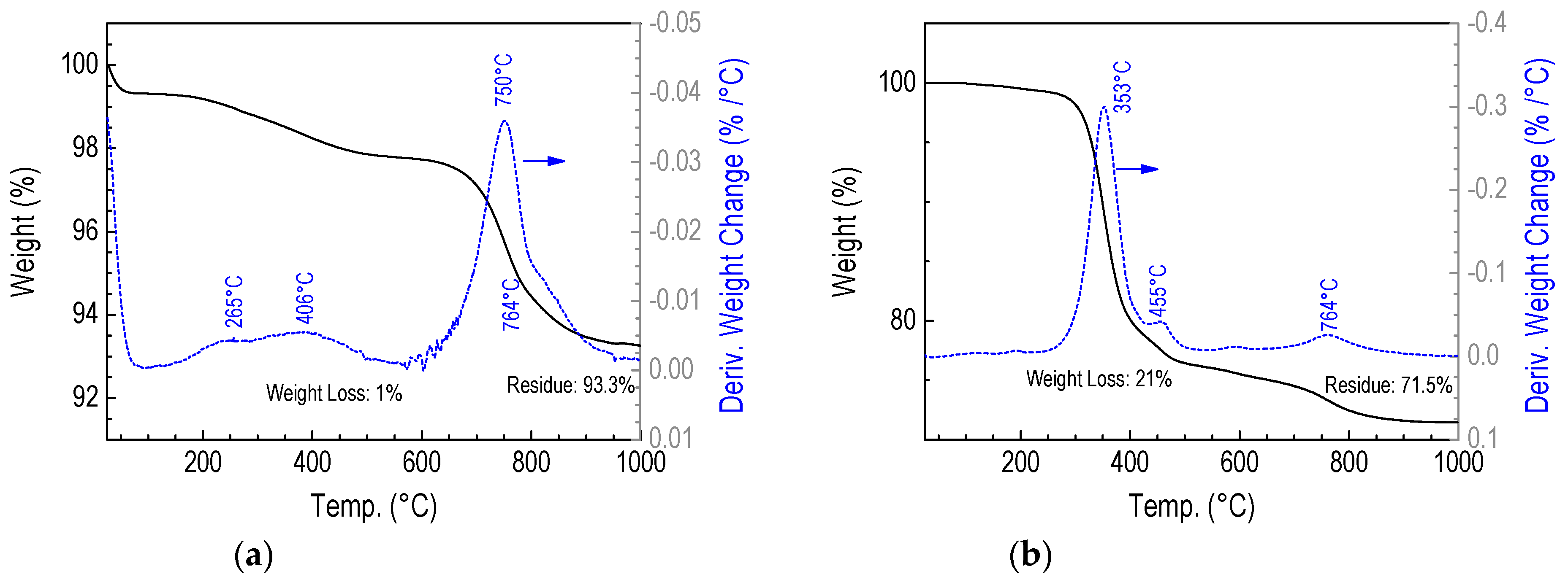
Two types of materials were tested: a D4H-CVD-30 °C layered deposit formed from D4H on an unheated substrate, and a CVD deposit from D4H gas-phase products that were evacuated from the reactor volume and collected in a cold trap (Figure 9).
The analysis of TGA in the nitrogen stream of two types of CVD deposits from Figure 9, i.e., produced in the reactor and products accumulated from the gas phase outside the reactor, tested in the temperature range of 25–1000 °C, is a continuous process, leading to small changes in mass loss. Up to 600 °C, only 1% of the mass in the material structure is lost, and up to 1000 °C 6.7%. Products created in the gas phase and evacuated from the reactor space are less thermally resistant and the main loss of mass in the amount of 21% occurs up to a temperature of 400 °C. At a temperature of 1000 °C, we observe a loss of 29.5%. The main product of CVD after pyrolysis at 1000 °C is silica as well as a certain amount of silicon oxycarbide with traces of amorphous carbon [29].

3.2.6. Elementary Chemical Reactions Occurring in the RHP-CVD Process with the Participation of the D4H Precursor

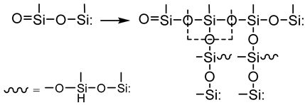
On the basis of the our previous studies of the chemical structure of CVD SiOC layers and literature data describing the reactions of methylsilanes with atomic hydrogen [30,31] and thermochemical processes occurring during low-pressure pyrolysis of polymethylcarbosilanes [32,33], hypothetical elemental reactions involved in the formation of silicon oxycarbide layers from tetramethylcyclotetrasilane were developed. The total process of layer growth can be divided into three stages: activation, growth, and cross-linking.
  • Activation step
No cyclic structures were found in the products of the layer deposited in the CVD reactor at 30 °C. The D4H molecule in the presence of hydrogen radicals can undergo a reaction in the gas phase leading to the opening of the ring, in a similar way to the fragmentation of the TMDSO molecule [17]. The resulting linear intermediate product has two reactive methylsilane and methylsilene centers at its ends (1).
Coatings 15 01179 i001
This product, having Si-H units, can further fragment in the presence of H• radicals, forming shorter silanone–disiloxane–silylene units (2):
Coatings 15 01179 i002a
A whole cycle can be fragmented at the same time:
Coatings 15 01179 i002b
  • Growth and networking stage
The methylsilene fragment can be isomerized to the silene biradical (3):
Coatings 15 01179 i003
and the silanone part is easily inserted into Si-O or reacted with a silene biradical to form branched structures (4):
Coatings 15 01179 i004
Also, the hydrosilyl units (MeHSiO) of reaction (1) can be converted to branched MeSiO1.5 units with the release of a methylsilane molecule:
Coatings 15 01179 i005
Cross-linking reactions can occur according to the scheme, leading to the formation of Si-CH2-Si carbosilane units:
Coatings 15 01179 i006
At room temperature, T-type units are formed with a large proportion of methyl groups in the structure. With increasing temperature, organic groups, e.g., –CH3, are rearranged and removed from the layer structure.

3.2.7. Analysis of Surface Morphology

Understanding the morphological structure of the layer surface is necessary due to their potential applications as intermediate layers or covering layers (with the possibility of further modification with organic compounds).
  • Scanning electron microscopy (SEM)
Studies of the surface morphology of the produced siliconoxycarbide layers were carried out using scanning electron microscopy (SEM) and atomic force microscopy (AFM). Figure 10 shows SEM images of the surface of layers deposited from D4H for the two extreme substrate temperatures of 30° and 350 °C.
The images show that on a micrometric scale, the surface of the layers is smooth, without defects, with high morphological homogeneity regardless of the substrate temperature. The absence of layers of characteristic powder structures on the surface indicates that in the RHP-CVD process, propagation occurs mainly on the growth surface and not in the gas phase.
  • Atomic force microscopy (AFM)
AFM measurements revealed some influence of substrate temperature on the film surface morphology at the nanometer scale. Figure 11 shows the film surface of selected samples prepared at TS temperatures of 30°, 100°, and 350 °C. The determined size of the root mean square Rrms from the measured altitude profile determines the surface roughness. The values of Rrms are shown as a function of the substrate temperature in Figure 11d.
From these relationships, it can be seen that the surface roughness Rrms of the studied silicon oxycarbide layers in the range up to 75 °C is low below 1 nm. At a temperature of approx. TS = 100 °C, it rapidly rises above 2.2 nm, and then, with an increase in substrate temperature to 250 °C, it decreases to approx. 1 nm. For TS ≥ 250 °C, the values of the mean square surface roughness are in the range of very small values of 0.7 nm ≤ Rrms ≤ 0.5 nm. The values of profile changes as a function of temperature are reflected in the surface morphology, which at 30 °C has the character of continuous undulations with the presence of isolated “hills”. However, already at 100 °C, globular structures with diameters of 70–100 nm begin to form, which dominate at temperatures TS > 250 °C, and their size is reduced to 30–50 nm. The observed temperature dependence of the surface roughness of the layers is a complex phenomenon that may result from the thermally activated surface mobility of layer-forming precursors formed in the gas phase and from the processes of layer cross-linking. Both of these factors may be responsible for the formation of fairly homogeneous globules, and their small size causes the effect of smoothing the surface. This behavior can be explained by the fact that at higher temperatures of the TS substrate, the surface of layer growth is quite mobile, which, combined with chemical reactions, causes its strong cross-linking leading to the formation of a high-density material. The diagram shows that for high substrate temperatures, the surface roughness approaches the value of Rrms = 0.5 nm, i.e., close to the roughness of the native substrate c–Si (Rrms Si = 0.3 nm).
The low surface roughness of the studied layers indicates the possibility of producing morphologically homogeneous silicon oxycarbide thin-film materials on substrates with complex surface topography in the hydrogen-initiated CVD process.
  • Conformal step coverage
The assessment of the uniformity of the coating thickness of the produced layers and the surface mobility of the layer-forming precursors was carried out on the basis of tests of the conformity of substrate mapping during CVD coating. Figure 12 shows SEM images of the fracture of a trapezoidal groove substrate at the micrometer scale, covered with a layer made of D4H at a substrate temperature of 350 °C. These images show that the layer thicknesses at the bottom of the groove, on the side walls, and on the surface are similar, indicating conformal mapping of the substrate. Such a coating is formed in the presence of layer-forming precursors with high surface mobility and low reactivity [34]. SEM images suggest that CVD ceramic films produced at temperatures above 300 °C are distinguished by very high homogeneity, difficult to obtain with other plasma methods [35]. This may be due to both the precursor used and the RHP-CVD method, which, due to the defined reaction initiating the plasmochemical process, also leads to homogeneous deposition on substrates with a complex profile, the so-called conformal coating. An important parameter characterizing complex topological covers is the aspect ratio (AR). The AR is the ratio of the height to the width of the groove. The conformality of the cover is measured using the step coverage parameter, which is the ratio of the thickness of the deposited layer at the bottom to its thickness at the groove wall. In the case of the siloxane precursor—TMDSO—the uniformity of a similar grooved substrate was approximately 95%. Generally, RHP-CVD is observed to provide a very high degree of coverage, which can be attributed to the presence of layer-forming decomposition products of the precursors, capable of rapid migration across the surface. This particularly advantageous property of remote hydrogen plasma processes has also been observed for a-sSiC:H layers produced from a methylsilane [36] (dimethylsilyl)(trimethylsilyl)methane [34] precursor and CVD a-SiO2 layers produced in remote oxygen plasma from tetraethoxysilane (TEOS) [37].

3.3. Physical and Physicochemical Properties of D4H-CVD Layers

Studies on the basic physical, physicochemical, mechanical, and optical properties of the produced silicon carbon layers as a function of changes in the deposition temperature were performed.
  • Density of D4H-CVD
Measurements of the density (ρ) of layers of different thicknesses, which can be controlled by deposition time, indicate their high physical homogeneity and constant density. The density of the layers was determined by measuring the mass of the deposited layer on a microscope slide of known surface and thickness, which was obtained from ellipsometric measurements. The determined densities for different substrate temperatures Ts in the range of 30–350 °C are shown in Figure 13.
As the deposition temperature of the TS layers increases, the density value ρ increases slightly in the range of values of 1.35–1.5. Only from ~200 °C is a significant increase to ρ ≈ 2.5 observed. This change is interpreted by the increasing degree of atom packing caused by the elimination of Si–CH3 organic groups absorbing at 2974 and 1277 cm−1 (visible decrease in the intensity of these IR bands), occurring at higher substrate temperatures. The increase in density is the result of the previously described changes occurring in the chemical structure of the layers and cross-linking processes, leading to the formation of Si–O and Si–C bonds and the transformation of the layer from a polymer-like material for low temperatures to a ceramic-like material created for higher substrate temperatures with visible elimination of Si–CHx- groups. The low density for Ts < 200 °C (~1.5 g∙cm−3) is probably due to the presence of cyclic/cavity structures with a low degree of cross-linking. Note that the density of the D4H precursor (ρ = 0.991 g∙cm−1) is significantly lower.
  • Refractive index of CVD layers
The optical properties of the layers were determined by spectroscopic ellipsometry. To determine the thickness and optical parameters n (λ) and k (λ), i.e., the refractive index (RI) and the extinction coefficient of the layer, corresponding to the structure of the measured optical system, respectively, the Cauchy–Urbach dispersion model was used as a fitting model for ellipsometric data. The obtained values of the n coefficient depending on the substrate temperature are shown in Figure 14.
Figure 14 shows that the nature of changes in the refractive index n is similar to the dependence of the density ρ on TS; i.e., initially in the range of 30–200 °C, it changes slowly in the range of 1.432–1.438. Then, with an increase in the substrate temperature above 200 °C, the index n changes significantly, reaching a not-very-high maximum value of n = 1.484. It is worth noting that the measured values of the refractive index are lower than 1.5 and differ from the previously described values for SiOC layers produced, for example, from the TMDSO precursor [17] (n = 1.7) or from 2D2 [21] (n = 1.6). Low values should be associated with the dominant content of Si–O bonds in the 3D structure of the SiOC network and the presence of vacancies. Increasing the Si–O content in the layer cross-linking process causes a limited increase in the refractive index n.
  • Photoluminescence of CVD layers
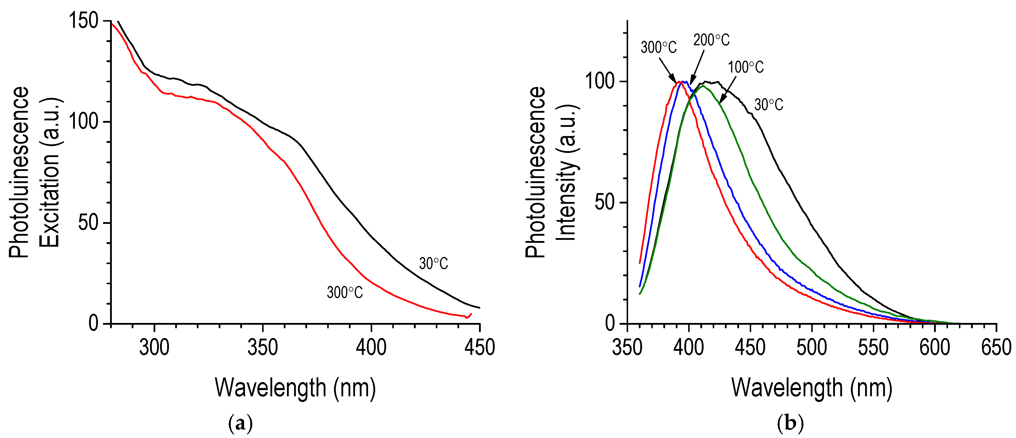
Photoluminescence (PL) studies of the studied layers show that they are characterized by a wide emission spectrum, with a blue–white spectrum observed with the naked eye (excitation with a UV lamp at a wavelength of 320–370 nm). We analyzed the emission spectra (λex = 350 nm) and photoluminescence excitation spectra (λem = 450 nm) for the layers deposited at different substrate temperatures. The results for different substrate temperatures (TS) normalized to the intensity at the PL maximum are presented in Figure 15. All emission spectra are characterized by a single asymmetric band, with a maximum in the wavelength range of λ = 390–420 nm, depending on the deposition temperature. These results are consistent with data published by other research teams [38,39]. Increasing TS causes a shift of the PL maximum toward higher energies (hypsochromic effect) and a decrease in the spectral half-width. On the other hand, the excitation spectra, which generally reflect absorption, are broadband, with several peaks at 330 and 360 nm. With temperature increases, the long-wavelength tail of the spectrum decreases and shifts toward short wavelengths. The wide width of the emission bands is due to the presence of varying degrees of delocalization states formed during the deposition of the layers.
Particularly important in the electronic structure is the contribution of dandling bonds with excess or missing electrons and structures with silicon clusters that may be present in the layer. The energy width of these states, as shown by the spectra, decreases with increasing temperature. Similar studies of PL SiOC layers were carried out and described earlier [17].

4. Conclusions

The data for the thermally activated layer’s deposition rate shows that in the tested substrate temperature range TS = 30–350 °C, the RHP-CVD process with the use of the D4H cyclic precursor proceeds according to two mechanisms with different activation parameters. On the basis of the results of FTIR and 13C and 29Si CP/MAS NMR studies, it was found that the layers produced in the low-temperature range contain structural fragments derived from the parent precursors, including not only the unreacted methylsilyl and ethoxysilyl functional groups, but also newly formed silanol groups. At high temperatures, densely packed lattice structures are observed with a small presence of organic groups CHx (x < 3). This means that the increase in TS is associated with the elimination of organic groups and subsequent cross-linking through the formation of a backbone Si–O–Si network with a rather low presence of carbide/hydrocarbon units. The process of elimination above 125 °C is also manifested by a drastic increase in density and an increase in the refractive index. The RI (n) of the a-SiOC layers in the range of TS = 30–125 °C reaches the minimum value, which can be attributed to the formation of a porous deposit structure. A reduction in the RI value of thin films can also be achieved by high-temperature annealing of the product. This process was clearly observed for the layer formed at TS = 30 °C. The refractive index RI decreased from 1.49 to 1.42 after aging at 600 °C in the N2 atmosphere. In this case, as shown by FTIR studies, thermal aging led to partial elimination of organic groups from the structure and formation of new Si–O–Si siloxane bonds as a result of condensation of Si–OH silanol groups. The porosity of the material is evidenced by the presence of a more intense slope at 1135 cm−1 in relation to the main maximum of the Si–O–Si vibration band at 1040 cm−1. The formation of additional Si–O–Si bonds as a result of thermal aging improves the mechanical properties of the deposit.
In light of the AFM and SEM tests, the SiOC layers are defect-free materials, are morphologically homogeneous and have a low surface roughness. However, the roughness of their surface increases with increasing temperature, which contrasts with the changes in surface roughness of layers produced from other organosilicon precursors observed in the further part of the paper. The observed surface roughness with the increase in TS is attributed to the reduced surface mobility of the layer-forming molecules and their high adhesion coefficient. Lower surface mobility of adsorbent molecules may slightly impair coating properties as observed in SEM studies of SiOC-coated groove substrates.
The selectivity of reactions induced by atomic hydrogen also promotes the transformation of alkoxy groups into silyl radicals or silanol groups, which easily undergo reactions leading to the formation of a siloxane network. This process leads to a decrease in RI to the observed value of 1.40. At high substrate temperatures, thermochemical reactions predominate, as a result of which the alkyl silyl groups of the precursor are transformed into Si–C carbide structures. In our work, we presented the most probable mechanism of cross-linking and layer formation, which is a significant step towards understanding the mechanism of obtaining this type of coatings by the CVD method.
Deposition of SiOC films from tetramethylcyclotetrasiloxane CVD can provide excellent conformal step coverage and create uniformly thick vertical coating with excellent protective properties. Overlay SiOC coatings can also be modified with active functional groups for various applications.

Author Contributions

Conceptualization, A.W.-P. and K.J.; methodology, A.W.-P. and K.J.; formal analysis, A.W.-P.; investigations, A.W.-P., K.J., and R.B.; resources, A.W.-P. and K.J.; data curation, A.W.-P.; writing—original draft preparation, A.W.-P. and P.U.; writing—review and editing, A.W.-P. and P.U.; visualization, A.W.-P., K.J., J.Z., and R.B.; supervision, P.U. All authors have read and agreed to the published version of the manuscript.

Funding

This research received no external funding.

Institutional Review Board Statement

Not applicable.

Informed Consent Statement

Not applicable.

Data Availability Statement

The original contributions presented in this study are included in the article. Further inquiries can be directed at the corresponding author.

Conflicts of Interest

The authors declare no conflicts of interest.

Abbreviations

The following abbreviations are used in this manuscript:
CVDChemical Vapor Deposition
RHPRemote Hydrogen Plasma
AFMAtomic Force Microscopy
HTPHydride Transfer Process
PLPhotoluminescence
XPSX-ray Photoelectron Spectroscopy
D4H1,3,5,7-tetracyclotetrasiloxane
TMDSO1,1,3,3-tetramethyldisiloxane
TGAThermogravimetric analysis
EDSEnergy Dispersive X-ray Spectroscopy
SEMScanning Electron Microscopy
M, D, T, QSi structures with a specific number of adjacent oxygen atoms, one, two, three and four, respectively

References

  1. Riedel, R.; Mera, G.; Hauser, R.; Klonczynski, A. Silicon-based polymer-derived ceramics: Synthesis properties and applications-a review dedicated to Prof. Dr. Fritz Aldinger on the occasion of his 65th birthday. J. Ceram. Soc. Jpn. 2006, 114, 425–444. [Google Scholar] [CrossRef]
  2. Godavarthi, S.; Wang, C.; Verdonck, P.; Matsumoto, Y.; Koudriavtsev, I.; Dutt, A.; Tielens, H.; Baklanov, M. Study of porogen removal by atomic hydrogen generated by hot wire chemical vapor deposition for the fabrication of advanced low-k thin films. Thin Solid Film. 2015, 575, 103–106. [Google Scholar] [CrossRef]
  3. Islam, M.Z.; Fu, Y.; Deb, H.; Hasan, M.K.; Dong, Y.; Shi, S. Polymer-based low dielectric constant and loss materials for high-speed communication network: Dielectric constants and challenges. Eur. Polym. J. 2023, 200, 112543. [Google Scholar] [CrossRef]
  4. Salehi, M.M.; Mohammadi, M.; Akbarzadeh, A.R.; Babamoradi, M.; Maleki, A.; Zare, E.N. Advancements in preceramic inorganic polymers for environmental applications: Properties, synthesis, and potential uses. RSC Adv. 2025, 15, 25514–25541. [Google Scholar] [CrossRef]
  5. Mazo, M.A.; Padilla, I.; López-Delgado, A.; Tamayo, A.; Rubio, J. Silicon Oxycarbide and Silicon Oxycarbonitride Materials under Concentrated Solar Radiation. Materials 2021, 14, 1013. [Google Scholar] [CrossRef]
  6. Chen, J.; King, S.W.; Muthuswamy, E.; Koryttseva, A.; Wu, D.; Navrotsky, A. Thermodynamic Stability of Low-k Amorphous SiOCH Dielectric Films. J. Am. Ceram. Soc. 2016, 99, 2752–2759. [Google Scholar] [CrossRef]
  7. Yang, H.; Chen, Y.; Wah Wong, M. Generating amorphous SiOC:H Structure: A novel Unit-Cell algorithm and its application in low-k porous material simulations. Comput. Mater. Sci. 2024, 242, 113093. [Google Scholar] [CrossRef]
  8. Yuan, C.; van der Sluis, O.; Zhang, G.Q.; Ernst, L.J.; Driel, W.; van silfhout, R.; Thijsse, B. Chemical–mechanical relationship of amorphous/porous low-dielectric film materials. Comput. Mater. Sci. 2007, 42, 606–613. [Google Scholar] [CrossRef]
  9. Ramos-Serrano, J.R.; Matsumoto, Y.; Ávila, A.; Romero, G.; Meneses, M.; Morales, A.; Luna, J.A.; Flores, J.; Minquiz, G.M.; Moreno-Moreno, M. Luminescence Study of Hydrogenated Silicon Oxycarbide (SiOxCy:H) Thin Films Deposited by Hot Wire Chemical Vapor Deposition as Active Layers in Light Emitting Devices. Inorganics 2024, 12, 298. [Google Scholar] [CrossRef]
  10. Grill, A. From tribological coatings to low-k dielectrics for ULSI interconnects. Thin Solid Film. 2001, 398–399, 527–532. [Google Scholar] [CrossRef]
  11. Du, P.; Wang, X.; Lin, I.K.; Zhang, X. Effects of composition and thermal annealing on the mechanical properties of silicon oxycarbide films. Sens. Actuators A Phys. 2012, 176, 90–98. [Google Scholar] [CrossRef]
  12. Plummer, J.D. Silicon VLSI Technology: Fundamentals, Practice, and Modeling; Pearson Education India: Delhi, India, 2009. [Google Scholar]
  13. Arango Ospina, M.; Xie, F.; Gonzalo de Juan, I.; Riedel, R.; Ionescu, E.; Boccaccini, A. Review: Silicon oxycarbide based materials for biomedical applications. Appl. Mater. Today 2019, 18, 100482. [Google Scholar] [CrossRef]
  14. Zhuo, R.; Colombo, P.; Pantano, C.; Vogler, E.A. Silicon oxycarbide glasses for blood-contact applications. Acta Biomater. 2005, 1, 583–589. [Google Scholar] [CrossRef]
  15. Böke, F.; Giner, I.; Keller, A.; Grundmeier, G.; Fischer, H. Plasma-Enhanced Chemical Vapor Deposition (PE-CVD) yields better Hydrolytical Stability of Biocompatible SiOx Thin Films on Implant Alumina Ceramics compared to Rapid Thermal Evaporation Physical Vapor Deposition (PVD). ACS Appl. Mater. Interfaces 2016, 8, 17805–17816. [Google Scholar] [CrossRef]
  16. Mizerska, U.; Rubinsztajn, S.; Chojnowski, J.; Cypryk, M.; Uznanski, P.; Walkiewicz-Pietrzykowska, A.; Fortuniak, W. Self-Restructuring of Polyhydromethylsiloxanes by the Hydride Transfer Process: A New Approach to the Cross-Linking of Polysiloxanes and to the Fabrication of Thin Polysiloxane Coatings. Materials 2022, 15, 6981. [Google Scholar] [CrossRef]
  17. Wrobel, A.M.; Uznanski, P.; Walkiewicz-Pietrzykowska, A. Silicon Oxycarbide Films Produced by Remote Microwave Hydrogen Plasma CVD using a Tetramethyldisiloxane Precursor: Growth Kinetics, Structure, Surface Morphology, and Properties. Chem. Vap. Depos. 2015, 21, 307–318. [Google Scholar] [CrossRef]
  18. Uznanski, P.; Walkiewicz-Pietrzykowska, A.; Jankowski, K.; Zakrzewska, J.; Wrobel, A.M.; Balcerzak, J.; Tyczkowski, J. Atomic Hydrogen Induced Chemical Vapor Deposition of Silicon Oxycarbide Thin Films Derived from Diethoxymethylsilane Precursor. Appl. Organomet. Chem. 2020, 34, e5674. [Google Scholar] [CrossRef]
  19. Agnieszka, W.-P.; Pawel, U.; Aleksander, M.W. Silicon Carbide, Silicon Carbonitride, and Silicon Oxycarbide Thin Films Formed by Remote Hydrogen Microwave Plasma CVD. Curr. Org. Chem. 2017, 21, 2229–2239. [Google Scholar] [CrossRef]
  20. Uznanski, P.; Glebocki, B.; Walkiewicz-Pietrzykowska, A.; Zakrzewska, J.; Wrobel, A.M.; Balcerzak, J.; Tyczkowski, J. Surface modification of silicon oxycarbide films produced by remote hydrogen microwave plasma chemical vapour deposition from tetramethyldisiloxane precursor. Surf. Coat. Technol. 2018, 350, 686–698. [Google Scholar] [CrossRef]
  21. Walkiewicz-Pietrzykowska, A.; Jankowski, K.; Kurjata, J.; Dolot, R.; Brzozowski, R.; Zakrzewska, J.; Uznanski, P. Silicon Oxycarbide Thin Films Produced by Hydrogen-Induced CVD Process from Cyclic Dioxa-Tetrasilacyclohexane. Materials 2025, 18, 2911. [Google Scholar] [CrossRef]
  22. King, S.W.; French, M.; Bielefeld, J.; Lanford, W.A. Fourier transform infrared spectroscopy investigation of chemical bonding in low-k a-SiC:H thin films. J. Non-Cryst. Solids 2011, 357, 2970–2983. [Google Scholar] [CrossRef]
  23. Raynaud, P.; Despax, B.; Segui, Y.; Caquineau, H. FTIR Plasma Phase Analysis of Hexamethyldisiloxane Discharge in Microwave Multipolar Plasma at Different Electrical Powers. Plasma Process. Polym. 2005, 2, 45–52. [Google Scholar] [CrossRef]
  24. Vautrin-Ul, C.; Roux, F.; Boisse-Laporte, C.; Pastol, J.L.; Chausse, A. Hexamethyldisiloxane (HMDSO)-plasma-polymerised coatings as primer for iron corrosion protection: Influence of RF bias. J. Mater. Chem. 2002, 12, 2318–2324. [Google Scholar] [CrossRef]
  25. Wu, Q.; Gleason, K.K. Plasma-Enhanced CVD of Organosilicate Glass (OSG) Films Deposited from Octamethyltrisiloxane, Bis(trimethylsiloxy)methylsilane, and 1,1,3,3-Tetramethyldisiloxane. Plasmas Polym. 2003, 8, 31–41. [Google Scholar] [CrossRef]
  26. Launer, P.; Arkles, B. Infrared Analysis of Organosilicon Compounds. In Silicon Compounds: Silanes & Silicones; Gelest Inc.: Glen Rock, PA, USA, 2013; pp. 175–178. [Google Scholar]
  27. Smith, A.L. Infrared spectra-structure correlations for organosilicon compounds. Spectrochim. Acta 1960, 16, 87–105. [Google Scholar] [CrossRef]
  28. Yu, S.; Tu, R.; Goto, T. Preparation of SiOC nanocomposite films by laser chemical vapor deposition. J. Eur. Ceram. Soc. 2015, 36, 403–409. [Google Scholar] [CrossRef]
  29. Ma, J.; Shi, L.; Shi, Y.; Luo, S.; Xu, J. Pyrolysis of polymethylsilsesquioxane. J. Appl. Polym. Sci. 2002, 85, 1077–1086. [Google Scholar] [CrossRef]
  30. Ellul, R.; Potzinger, P.; Reimann, B. Reaction of hydrogen atoms with hexamethyldisilane. J. Phys. Chem. 1984, 88, 2793–2796. [Google Scholar] [CrossRef]
  31. Fabry, L.; Potzinger, P.; Reimann, B.; Ritter, A.; Steenbergen, H.P. Gas-phase homolytic substitution reactions of hydrogen atoms at silicon centers. Organometallics 1986, 5, 1231–1235. [Google Scholar] [CrossRef]
  32. Yajima, S.; Hasegawa, Y.; Hayashi, J.; Iimura, M. Synthesis of continuous silicon carbide fibre with high tensile strength and high Young’s modulus. J. Mater. Sci. 1978, 13, 2569–2576. [Google Scholar]
  33. Birot, M.; Pillot, J.-P.; Dunogues, J. Comprehensive Chemistry of Polycarbosilanes, Polysilazanes, and Polycarbosilazanes as Precursors of Ceramics. Chem. Rev. 1995, 95, 1443–1477. [Google Scholar] [CrossRef]
  34. Wróbel, A.M.; Walkiewicz-Pietrzykowska, A.; Klemberg-Sapieha, J.E.; Nakanishi, Y.; Aoki, T.; Hatanaka, Y. Remote Hydrogen Plasma Chemical Vapor Deposition from (Dimethylsilyl)(trimethylsilyl)methane. 1. Kinetics of the Process; Chemical and Morphological Structure of Deposited Silicon−Carbon Films. Chem. Mater. 2003, 15, 1749–1756. [Google Scholar] [CrossRef]
  35. Baxamusa, S.H.; Gleason, K.K. Thin Polymer Films with High Step Coverage in Microtrenches by Initiated CVD. Chem. Vap. Depos. 2008, 14, 313–318. [Google Scholar] [CrossRef]
  36. Wrobel, A.M.; Walkiewicz-Pietrzykowska, A.; Uznanski, P. Remote hydrogen microwave plasma chemical vapor deposition from methylsilane precursors. 2. Surface morphology and properties of deposited a-SiC:H films. Thin Solid Film. 2014, 564, 232–240. [Google Scholar] [CrossRef]
  37. Wróbel, A.M.; Walkiewicz-Pietrzykowska, A.; Wickramanayaka, S.; Hatanaka, Y. Mechanism of Amorphous Silica Film Formation from Tetraethoxysilane in Atomic Oxygen-Induced Chemical Vapor Deposition. J. Electrochem. Soc. 1998, 145, 2866–2876. [Google Scholar] [CrossRef]
  38. Coyopol, A.; Garcia-Salgado, G.; Díaz-Becerril, T.; Vásquez-Agustín, M.A.; Romano-Trujillo, R.; López, R.; Rosendo, E.; Nieto-Caballero, F.G.; Morales-Ruiz, C.; Morales-Sanchez, A. Strong white light emission from SiCxOy films grown by HFCVD technique. Opt. Mater. 2020, 99, 109551. [Google Scholar] [CrossRef]
  39. Oh, T. Photoluminescence characteristics of SiOC thin films deposited by using inductively coupled plasma chemical vapor deposition with annealing. Inf. Int. Interdiscip. J. 2013, 16, 1391–1397. (In Japanese) [Google Scholar]
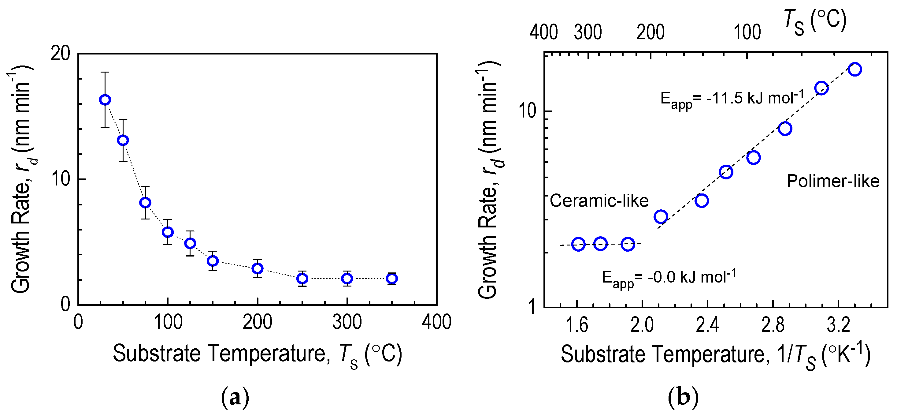
Figure 1. (a) Thickness rate of growth of the layer sourced from the D4H precursor as a function of substrate temperature. (b) Arrhenius plot of the growth rate of the rd layer. Process conditions: F(D4H) = 5 sccm; F(H2) = 100 sccm; p = 70 W.
Coatings 15 01179 g001
Figure 2. FTIR transmission spectra of layers with a thickness of 380–600 nm, obtained from tetramethylcyclosiloxane at different TS substrate temperatures in the range of 30−350 °C.
Coatings 15 01179 g002
Figure 3. Transmission FTIR spectra of CVD−50 °C, CVD−125 °C, and CVD−350 °C layers with a thickness of ~200 nm for two angles of inclination of the sample in relation to the analysis beam: a-dashed line, θ = 0°, and b-solid line, θ = 70°. The 1195 cm−1 band can be attributed to LO vibrations, and the 1033 cm−1 band to TO vibrations of the amorphous network.
Coatings 15 01179 g003
Figure 4. Fragment of IR spectra of CVD layers from D4H with distribution into component bands made at substrate temperature TS = 50° (a), 125° (b), and 350 °C (c) at different sample inclination angles θ = 0° and 70°.
Coatings 15 01179 g004
Figure 5. FTIR-ATR spectra of deposits from the CVD reactor black line and from the cold trap located outside the reactor blue line.
Coatings 15 01179 g005
Figure 6. Photoelectron spectra of Si p and C1s of layers obtained from tetramethylcyclotetrasiloxane at substrate temperatures TS = 30°C (a), 75°C (b), 125°C (c), and 350 °C (d) with decomposition into Gaussian component bands.
Coatings 15 01179 g006
Figure 7. Temperature dependencies of the relative fraction of individual atoms Si2p, C1s, and O1s in the surface zone of layers obtained from tetramethylcyclotetrasiloxane in the range TS = 30–350 °C determined in XPS measurements (a). Percentage of individual elements in the volume of D4H-CVD layers as a function of substrate temperature TS obtained on the f EDS measurements (b). The percentage composition of the monomer is also indicated in the figures (open symbols).
Coatings 15 01179 g007
Figure 8. Spectra of 29Si CP/MAS NMR (a) and 13C CP/MAS NMR (b) of the D4H-CVD deposit, deposited at 30 °C in the CVD reactor (a, solid line), and the D4H-Freezer deposit, deposited in the cold trap outside the CVD reactor (b, blue line, dashed); black bar on the δ axis−positions of the D4H monomer NMR signals in CDCl3.
Coatings 15 01179 g008
Figure 9. Thermolysis plot of stratified deposit D4H−CVD-30 °C formed on unheated substrate (a) and CVD deposit frozen from the gas phase (b).
Coatings 15 01179 g009
Figure 10. SEM images of the surface of siliconoxycarbide coatings produced from cyclosiloxane D4H on crystalline silicon wafers at two extreme substrate temperatures of 30° (a) and 350 °C (b).
Coatings 15 01179 g010
Figure 11. AFM images of CVD layers deposited with cyclosiloxane D4H on c-Si substrate at TS = 30°, 100°, and 350 °C, denoted as (a), (b), and (c), respectively, and roughness values, based on the root mean square Rrms of the height profile of the layer surface, as a function of substrate temperature (d). The area of the entire AFM image was used to calculate Rrms.
Coatings 15 01179 g011
Figure 12. SEM image of the fracture of a substrate with a trapezoidal groove covered with a layer made of cyclosiloxane D4H-CVD-350 °C with a thickness of ~30 nm at TS = 350 °C. Coating conformity for a high groove AR = 7:1 is 76% (for a groove with AR = 2.5:1 is 95%).
Coatings 15 01179 g012
Figure 13. Dependence of the density of layers made of D4H as a function of the deposition temperature TS.
Coatings 15 01179 g013
Figure 14. The dependence of the refractive index n for the wavelength λ = 630 nm of layers made of D4H as a function of the substrate temperature TS.
Coatings 15 01179 g014
Figure 15. Photoluminescence spectra (PL) of layers made of D4H for different temperatures of the TS substrate normalized to the intensity at the maximum: (a) excitation spectrum and (b) emission spectrum.
Coatings 15 01179 g015
Table 1. Vibration bands observed in the IR spectrum of the D4H monomer and in the spectra of the CVD layers.
Vibration Assignment *Band Position (cm−1)
D4H
(Precursor)
CVD-30 °C TS = 30 °CCVD-175 °C TS = 175 °CCVD-250 °C TS = 250 °CCVD-350 °C TS = 350 °C
νas(CH3)296729672974--
νs(CH3)290729072916--
νas(Si–H)21682240---
δas(CH3) in Si-(CH3)141114111413--
δ(Si–CH2–)-13611364-
δs(CH3) in Si-(CH3)12621274127612771277
νas(Si–O–Si)10961125 sh1114 sh1122 sh1155 sh
νas(Si–O–Si)1060 sh1062 sh---
νs(Si–O–Si)-1025103010421042
δ(Si–H)918 sh----
–O–SiHCH3890890---
ρ(CH3) CHw Si–(CH3)843840 sh832 sh831 sh-
Si–C (carbide) 800801
808
νs(Si–C) in Si–(CH3)769780780--
* vibration designations: ν—tensile; δ—bending; ρ—swinging (swinging); as—asymmetrical; s—symmetrical; sh—the ridge of the band.
Table 2. Photoelectron band components identified in the XPS spectra of CVD layers obtained from D4H.
Electron LevelNumber of Component BandsBinding Energy (eV)Half-Width
(eV)
Assigned
Structure
Si(2p)4101.3
102.7
103.5
103.8
1.1
1.1
1.2
Si–C
Si–O2
Si–O3
Si–O4
C(1s)2284.5
285.4
1.2
1.2
CHx, C–C
C–O–Si
O(1s)1532.41.2–1.4O–Si
Disclaimer/Publisher’s Note: The statements, opinions and data contained in all publications are solely those of the individual author(s) and contributor(s) and not of MDPI and/or the editor(s). MDPI and/or the editor(s) disclaim responsibility for any injury to people or property resulting from any ideas, methods, instructions or products referred to in the content.