Review

Phenomenological Analysis of Percolation Phenomena in Porous Low-k Dielectrics

by
Mungunsuvd Gerelt-Od
1,*,
Md Rasadujjaman
2,
Valerii E. Arkhincheev
3,
Konstantin A. Vorotilov
1 and
Mikhail R. Baklanov
1
1
Research and Educational Center “Technological Center”, MIREA—Russian Technological University (RTU MIREA), 78 Vernadsky Av., Moscow 119454, Russia
2
Department of Physics, Mawlana Bhashani Science and Technology University, Santosh, Tangail 1902, Bangladesh
3
Institute of Mathematics, Physics and Computer Sciences, Buryat State University, 24a Smolin St., Ulan-Ude 670000, Russia
*
Author to whom correspondence should be addressed.
Coatings 2025, 15(10), 1138; https://doi.org/10.3390/coatings15101138
Submission received: 29 August 2025 / Revised: 22 September 2025 / Accepted: 23 September 2025 / Published: 1 October 2025

Abstract

This work reviews percolation-related phenomena in porous organosilica glass (OSG) low-k dielectrics and their critical impact on mass transport, electrical conductivity, mechanical integrity, and dielectric breakdown. We discuss how leakage current arises from the formation of minimal percolating conductive paths along pores and defect chains, while dielectric breakdown requires system-spanning pore connectivity, resulting in a higher effective percolation threshold. Mechanical properties similarly degrade when pores coalesce into a connected network, exhibiting multiple percolation thresholds due to both chemical network modifications and porosity. Experimental trends demonstrate that leakage current increases sharply at low porosity, whereas breakdown voltage and mechanical stiffness collapse at higher porosity levels (~20%–30%). We highlight that distinct percolation classes govern transport, mechanical, and nonlinear phenomena, with correlation length and diffusion timescales providing a unified framework for understanding these effects. The analysis underscores the fundamental role of network connectivity in determining the performance of organosilicate glass-based ultra-low-k dielectrics and offers guidance for material design strategies aimed at simultaneously improving electrical, mechanical, and chemical robustness.

1. Introduction

The interest in low dielectric constant (low-k) films in microelectronics emerged in the late 1990s when it was recognized that, starting from the 90–130 nm technology nodes, signal propagation delays in the interconnects of ULSI (Ultra Large Scale Integrated) circuits began to exceed those at the transistor level. It became evident that this issue could be mitigated by reducing the resistance-capacitance (RC) delay in interconnects. Conductive wires needed lower resistance (R) compared to traditional aluminum, and the low-k intermetal dielectric had to replace traditional SiO2 and facilitate a reduction in capacitance (C). Aluminum (Al) was replaced by copper (Cu) due to its superior metallic conductivity and resistance to electromigration compared to aluminum (Al) [1,2,3].
The transition to Cu as the conductor was one of the most significant milestones in the history of semiconductor manufacturing. It required replacing the traditional subtractive process (metal etching followed by dielectric gap filling) with damascene technology. In this new approach, the dielectric is etched first, followed by metal gap filling using superfilling techniques. This technique must promote higher deposition rates at the bottom of trenches relative to the sidewalls, enabling void-free filling of trenches and vias. This technological shift demanded substantial modifications to the dielectric layers. The lower dielectric constant compared to traditional silicon oxide could be achieved either by using materials with low bond polarizability (e.g., organic polymers) or by employing silica-like materials with a high volume of nanometer-scale voids (pores) [4,5]. However, organic polymers (such as SiLK and Flare) were found to be largely incompatible with standard fabrication processes due to their poor integration with interconnect technology. One of the most critical issues is their high coefficient of thermal expansion (CTE) relative to other components of the integrated circuit [6]. As a result, the development of low-k dielectrics focused increasingly on porous silica-like (organosilica) materials [5,6,7,8,9].
The 1994 National Technology Roadmap for Semiconductors (NTRS)—the US predecessor of the International Technology Roadmap for Semiconductors (ITRS) [4]—projected that within 10 years the industry should be able to use dielectric materials with k < 1.5 (Figure 1). However, the real situation has been much more challenging and complicated.
In this figure, FOX is a fluorinated oxide (or FSG—Fluorinated Silicate Glass) with a dielectric constant k = 3.0–3.5. It was used for 130 and 180 nm technology nodes. BD1 is an organosilica glass (OSG) low-k film with a k value of 3.0, deposited via plasma-enhanced chemical vapor deposition (PECVD) without artificial porosity, and used in ULSI devices with technology nodes of 90 to 65 nm. These materials are represented by black squares as ULSI integrated components (Figure 1). SiLK is a dense organic polymer with a k value of 2.6. It was rejected by the microelectronics industry as a candidate for interconnect technology due to its poor compatibility, particularly its higher coefficient of thermal expansion (CTE) compared to other components of ULSI devices.
XLK, LKD, and NCS are typical representatives of highly porous ultralow-k (ULK) organosilica films [7]. However, they have generally not found real-world applications (except for NCS at Fujitsu) [12]. The main reason for their rejection is their porosity exceeding the percolation threshold (Table 1), leading to severe degradation during plasma and chemical processing and deterioration of mechanical and electrical properties. These findings highlight the importance of thoroughly analyzing percolation phenomena in porous low-k dielectrics for future ULSI technology.
One of the most difficult challenges in integrating these materials is also related to their hybrid (inorganic-organic) nature and inherent porosity. The hybrid nature arises from the incorporation of organic components, such as methyl groups, into the silica matrix [7]. Porous silica is naturally highly hydrophilic due to polar Si-OH bonds presence, and since the dielectric constant of adsorbed water is around 80, doping with organic groups is essential to maintain hydrophobicity and preserve low-k properties. However, these organic components possess different chemical properties from the silica matrix, making their concentration susceptible to change during various chemical treatments and plasma processes. For example, oxygen plasma—commonly used for resist stripping and cleaning—preferentially removes the organic groups, leading to an increase in the dielectric constant (k-value) and leakage current [13]. Porosity amplifies this effect, as the open structure of highly porous materials allows easier penetration of reactive species deep into the film, resulting in more extensive modification. The percolation threshold, which indicates the degree of pore interconnectivity, is obviously one of the key factors. Additionally, porous low-k materials are generally soft, mechanically weak, and do not adhere well to silicon or metal wires. Such low-k materials also exhibit higher leakage currents and a lower breakdown field.
As a result, the ITRS prediction that ultralow-k materials with a dielectric constant of approximately 1.5–1.7 would be integrated by around 2004 was not realized (Figure 1). A revised ITRS forecast published in 2006 projected the integration of materials with k = 2.5 starting in 2012. However, even this updated prediction also did not materialize.
The current strategy focuses on maintaining the k-value around 3.0 while reducing RC delay by introducing new conductive materials with lower resistance than copper (Cu) in narrow interconnect lines, along with thinner diffusion barriers [14]. The use of nearly dense low-k materials with k ≈ 3.0 with improved mechanical properties also enables the implementation of air gaps at selected metallization levels, further reducing overall RC delay. According to the latest edition of the IRDS (International Roadmap of Devices and Systems—the successor to the ITRS), materials with k ≈ 3.0 are expected to remain in use until at least 2029 [10]. However, projections beyond 2030 still envision the adoption of materials with k-values below 2.5. Currently, no viable non-porous options are known for achieving such low dielectric constants.
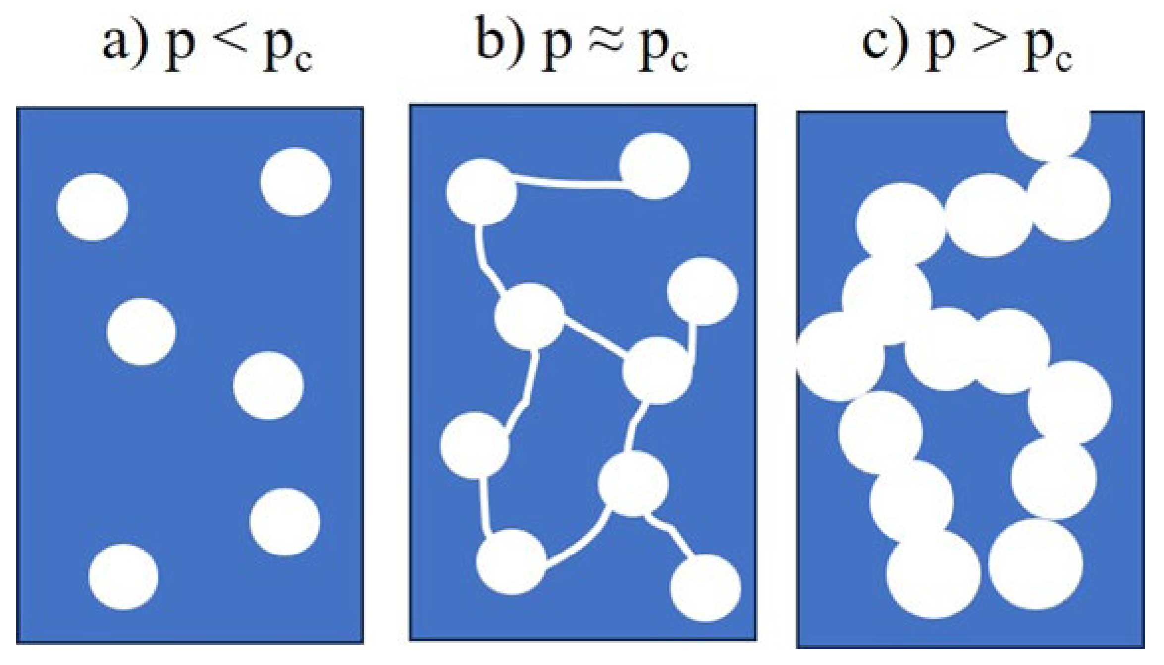
Figure 1 and Table 1 clearly show that a central concept governing these challenges is percolation—the formation of system-spanning networks of connected pores or defects (dashed line). The materials with porosity exceeding percolation threshold have not been successfully integrated so far. The percolation threshold denotes the critical porosity at which isolated pores transition into a continuous, interconnected pore network. This structural transition has profound implications for the material’s behavior. Below the threshold, the pores remain isolated or weakly connected, and the matrix retains much of its original barrier, mechanical, and dielectric properties. Above the threshold, however, continuous pathways emerge that facilitate the diffusion of moisture, reactive species, and contaminants; they also reduce mechanical strength and can significantly degrade the dielectric’s ability to insulate against electrical fields [7,8,9].
The percolation threshold thus serves as a critical structural limit in the design and processing of porous low-k materials. While lowering the dielectric constant by increasing porosity is desirable, approaching or crossing the percolation threshold can render the material mechanically fragile, chemically vulnerable, and electrically unstable. For instance, plasma radicals and moisture can penetrate deep into the dielectric via percolated pore networks, leading to irreversible modifications such as carbon depletion, silanol formation, and densification. Mechanically, interconnected pores can act as stress concentrators, lowering the elastic modulus and fracture toughness, and increasing susceptibility to damage during chemical mechanical polishing (CMP) or packaging-induced stress. Electrically, percolation may enable leakage pathways that compromise insulation and raise the risk of dielectric breakdown.
From the standpoint of microstructural engineering, percolation introduces a complex interplay between pore size, shape, distribution, orientation, and connectivity. Achieving a low dielectric constant while maintaining structural integrity requires careful tuning of these parameters through deposition conditions, porogen loading, curing strategies, and post-deposition treatments. Advanced characterization techniques such as positron annihilation lifetime spectroscopy (PALS) [15], ellipsometric porosimetry (EP) [16], and FIB-TEM tomography [17] have revealed how even small changes in pore architecture can shift the system toward or away from percolation behavior.
This review aims to provide a comprehensive assessment of percolation phenomena in porous low-k dielectrics, emphasizing the structure–property relationships that underpin mass transport, mechanical, and electrical behavior. The structure of this review is as follows:
  • Section 2 examines mass transport mechanisms in porous low-k films, with a focus on how percolation controls diffusivity and reactive species infiltration, including the role of percolated networks in facilitating the diffusion of stable molecules, plasma radicals, and environmental contaminants.
  • Section 3 explores how percolation affects key electrical properties, including permittivity, breakdown voltage, and dielectric degradation, particularly emphasizing how percolation alters dielectric breakdown strength, leakage currents, and long-term reliability.
  • Section 4 discusses the mechanical consequences of percolation, including stress localization, fracture pathways, and mechanical failure modes, with an emphasis on how pore connectivity impacts elastic modulus, hardness, toughness, and reliability under mechanical stress.
  • The conclusion highlights the broader implications of percolation for material design and outlines strategies for mitigating percolation-driven degradation while achieving ultra-low-k performance.
Understanding and controlling percolation phenomena is thus central to the development of next-generation dielectric materials. By bridging insights from microstructure characterization, transport theory, and mechanical modeling, this review aims to guide the design of porous low-k dielectrics that are both electrically superior and integration-ready.

2. Mass Transport and the Role of Percolated Networks in Facilitating the Diffusion of Stable Molecules, Plasma Radicals, Positronium (Ps) and Environmental Contaminants

2.1. Fabrication of Porous Low-k Films

Low-k films used in semiconductor manufacturing may exhibit constitutive porosity, which refers to inherent or intrinsic pores (voids) present within the material structure. In contrast, subtractive porosity typically describes intentionally introduced voids created during processing, such as through etching or the use of sacrificial porogens. Both types of porosity significantly influence the film’s overall dielectric properties and its suitability for specific applications in integrated circuit fabrication [7,16].
For example, materials like BD1 [18], which are deposited by PECVD with organosilane precursors without the use of sacrificial porogens, achieve reduced density and dielectric constant primarily due to a high volume of terminal organic groups that are replacing bridging oxygen atoms in silica like matrix. In sol–gel-based technologies, density reduction can be achieved during the aging process and through the hierarchical aggregation of primary sol particles. This reduction in density can be interpreted as porosity and is measurable using advanced techniques such as ellipsometric porosimetry (EP) [16] and positron annihilation lifetime spectroscopy (PALS) [15]. According to EP measurements, such films typically exhibit the total porosity levels below 10%–12%, with pore sizes comparable to that of the molecular probe used (e.g., a toluene molecule). Notable examples include the aforementioned BD1 and Aurora, developed by Applied Materials and ASM Japan in the early 2000s [8,19]. The porosity in these films is well below the predicted percolation threshold (~30%), which means they maintain robust mechanical integrity (Young’s modulus E > 10–15 GPa), show minimal degradation during plasma processing, and possess favorable electrical characteristics. These properties have enabled their successful integration into ultra-large-scale integration (ULSI) devices (Table 1).
The deposition of highly porous low-k films with a dielectric constant (k) below 2.7 typically requires the use of a sacrificial porogen (also referred to as a template in sol–gel films). This porogen in PECVD processes is usually a relatively volatile organic polymer, whose precursor is co-deposited with the matrix material. While the preparation of surfactant-templated sol–gel materials predates the development of low-k dielectrics [20], integrating sacrificial porogens into PECVD processes—preferred by the microelectronics industry—posed a much greater challenge. This technology was pioneered and developed at IBM by a team led by A. Grill [21,22]. Today, it has become a standard approach widely adopted by both researchers and semiconductor manufacturers.
During processing, an initial thermal treatment of deposited films at moderate temperatures (typically 150–200 °C) stabilizes and cross-links the matrix while the porogen mainly remains intact [23]. Final porogen removal is carried out at higher temperatures (around 400–450 °C), where the polymer decomposes into small volatile fragments that can diffuse out of the film and desorb. This removal process is inherently slow (the procedure takes more than an hour), but it can be significantly accelerated using UV light, electron beams, or microwave radiation [24,25,26].

2.2. Types of Porosity and Mass Transport

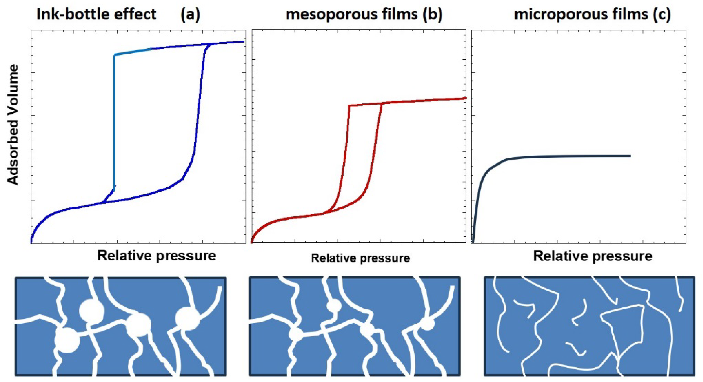
Figure 2 illustrates various types of low-k films fabricated using different deposition techniques, along with the corresponding adsorption isotherms obtained through adsorption porosimetry. Figure 2a demonstrates the so-called ink-bottle effect [27,28], where the material contains large internal voids—reflected in the adsorption branch—connected to the atmosphere through narrower necks, which influence the shape of the desorption branch. Such low-k films typically exhibit very high porosity, often exceeding 50%–60%, and are commonly deposited via sol–gel methods using polymeric templates with large feature sizes [28,29,30,31].
Figure 2b represents the typical behavior of most ultralow-k (ULK) films, which exhibit porosity levels ranging from 30% to 50% and corresponding dielectric constants (k-values) between approximately 2.5 and 2.0. The isotherm still displays a hysteresis loop, commonly interpreted as evidence of internal voids whose sizes are comparable to those of the connecting necks. The initial part of the isotherm (at near-zero relative pressure) suggests the presence of micropores, which, as already mentioned, are typically indicative of organic groups. Such films can be deposited using both PECVD and sol–gel techniques.
Figure 2c depicts microporous low-k films deposited without the use of sacrificial porogen; hence, the observed porosity is constitutive, originating from the intrinsic structure of the material. These films typically exhibit no hysteresis in their adsorption isotherms and have porosity levels below 15%. Representative examples include early versions of BD1 and Aurora. Some pores may be isolated—i.e., not connected to the atmosphere—and thus inaccessible to adsorbates during adsorption porosimetry. However, in the case of ellipsometric porosimetry, the volume of such closed pores can be indirectly estimated from the calculated refractive index of the matrix [16,28,29,30].
The pore size distribution, particularly in materials with multiple types of isolated voids, can be effectively assessed using PALS. However, the size of open pores can only be measured in samples with ‘capped’ pores, for instance, by depositing thin SiNx films. PALS also provides information on pore connectivity by measuring the depth from which positronium (Ps) can escape to vacuum, where it exhibits its characteristic lifetime of 142 ns. While materials shown in Figure 2a,b appear fully interconnected according to adsorption porosimetry, some of them show limited positronium diffusivity, as detected by PALS. This discrepancy between adsorption porosimetry and PALS data introduces uncertainty in defining the percolation threshold for mass transport in low-k films.
Extensive cross-evaluation of various low-k films deposited with different porogen concentrations (ranging from 0% to 50%) was carried out using EP and PALS techniques [32,33]. EP measurements, performed on all samples [33], revealed that most pores are accessible for adsorption and, therefore, remain interconnected even at porogen loadings well below 20%. In contrast, PALS results indicate that pore interconnectivity becomes restricted when the porogen concentration reaches approximately 20%–25%, despite both EP and PALS showing similar pore size measurements. A similar discrepancy between the diffusion of stable molecules and positronium was also observed in earlier studies, where degree and length of pore interconnectivity was evaluated using a specialized technique based on the diffusion of organic solvents [34] and the results compared with PALS data [35].
Therefore, the commonly accepted idea that the percolation threshold for mass transfer is close to 30% may have a more nuanced meaning. While this threshold is theoretically predicted by percolation theory, it strictly depends on the topology and dimensionality of the system. For example, site percolation on a 3D cubic lattice yields a threshold of approximately 0.31, while continuum percolation models—such as those involving overlapping spheres or pores—can produce similar or slightly different values depending on the shape and size distribution.
In the context of low-k films, the matrix (or wall) inherently contains small voids and channels due to the relatively large size of organic components (CH3). Moreover, as already mentioned, additional micropores of molecular size can form during the removal of porogen fragments. Stable molecules can slowly diffuse through these pores if their diameter is larger than that of the diffusing molecules. However, the situation becomes more complex with unstable species like free radicals formed in the plasma. In this case, their lifetime is drastically reduced due to collisions with the pore wall (surface recombination), leading to deactivation before they can diffuse through the pores. The depth of active radicals penetration ( δ ) depends on effective diffusivity (Deff) and recombination rate constant (kr) as Equation (1):
δ = D e f f k r ,
In the case of low-k films the pore size is much less than 100 nm and therefore D e f f = p τ D K , where p is porosity, t is pores tortuosity and DK is Knudsen diffusion coefficient. The depth of penetration δ, as already mentioned, is smaller than the theoretical percolation length and also depends on chemical nature of active radicals. Consequently, researchers studying the depth of low-k modification may conclude that pore permeability is limited [13].
The estimation of penetration depth (Equation (1)) relies on the assumption of normal diffusion (Equation (2)):
< x 2 t > = D e f f t ~ D e f f k r ,
where <x2(t)> is the mean squared displacement (MSD) of a particle (or probe) as a function of time t.
However, in complex branched systems, which are typical of porous low-k films, transport often exhibits subdiffusive behavior, as described by Equation (3):
< x 2 t > ~ ( D e f f t ) γ ,
where γ is a critical subdiffusion exponent, determined primarily by the type and topology of branching. These anomalous transport properties are frequently interpreted in terms of the fractal dimension of the system, reflecting its inherent self-similarity. The branched diffusion in these materials can even reduce the depth of penetration due to small value of critical exponent 0.25 < γ < 0.5 [36,37]. Therefore, a possible way to reduce the penetration depth is to fabricate films with smaller and more tortuous pores.
The situation becomes even more complex for positronium (Ps). In addition to accelerated surface annihilation, Ps is subject to quantum mechanical constraints that hinder its diffusion from large pores into narrow necks due to differences in ground-state energy between large voids and small constrictions [38,39]. As a result, the effective permeability of pores—and consequently the apparent percolation threshold—is lower for Ps than for reactive radicals.
For practical applications, the diffusion of active radicals is more relevant than that of Ps, as it directly reflects the depth of modification in low-k films during plasma processing. This underscores the need for a clear distinction between different definitions of percolation thresholds. Classically, the percolation threshold pc is defined as the critical fraction of open pathways (pores, channels, or bonds) at which a connected path spanning the material first emerges, enabling macroscopic transport. In percolation theory:
  • p < pc → no continuous path exists → macroscopic transport is effectively zero.
  • p > pc → a connected network exists → transport becomes possible.
This threshold is purely geometric, depending only on the connectivity of the medium. In real mass transport scenarios, particularly in porous media or low-k films, molecules or radicals have a finite lifetime τ due to reaction, decay, or adsorption. If the paths are long or tortuous, species may not survive long enough to traverse the system, introducing a dynamic, lifetime-dependent percolation threshold pc (τ) > pc. For very short-lived species, geometrically connected paths may fail to contribute to macroscopic transport because the species decays before reaching the outlet. As τ → ∞ (e.g., stable species like toluene in EP), the effective percolation threshold converges to the geometric threshold. For finite τ, the effective threshold shifts upward: a higher fraction of open paths is required for successful transport within the species’ lifetime.

2.3. Depth Profile of Plasma-Induced Damage

Plasma damage to porous low-k materials is a multifaceted phenomenon encompassing chemical damage from neutral radicals formed during etching and resist stripping (e.g., O, H, F), ion-induced bond breakage and densification, and the impact of VUV photons. Together, these factors create a complex scenario that necessitates thorough analysis. Plasma damage can alter the chemical composition and mechanical properties of low-k materials, while also introducing electrically active defects. The chemical changes increase their susceptibility to moisture adsorption and the accumulation of organic impurities, both of which negatively affect the long-term reliability of integrated structures [13,24].

2.3.1. Damage by Active Radicals

A downstream plasma reactor was used for this purpose, where the influence of ion bombardment is negligibly small. In this setup, active radicals diffuse into the pores, react with the material, and convert the low-k film into a hydrophilic state. Oxygen radicals remove CH3 groups and form Si–OH, while hydrogen can break Si–CH3 bonds and hydrogenate the silicon, also contributing to hydrophilicity. Fluorine atoms generated in fluorocarbon plasma can attack the Si–O backbone, generating various defects such as oxygen deficient centers.
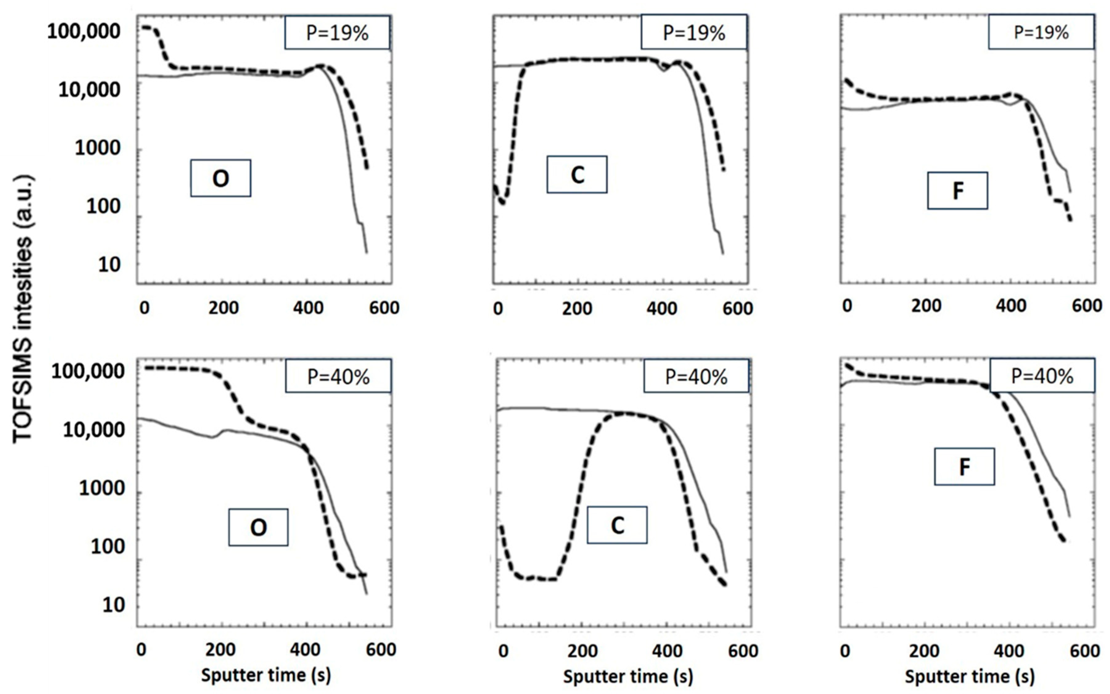
The top graphs in Figure 3 show plasma damage in low-k films with porosities below the theoretical percolation threshold (31%), while the bottom graphs illustrate the behavior of films with porosities above this threshold. The difference is especially pronounced with oxygen plasma, whereas fluorine plasma shows minimal variation. Oxygen plasma causes a significant reduction in carbon concentration and an increase in oxygen concentration, leading the upper layers of the films to adopt a silica-like composition. In the 19% porous film, the depth of modification was less than 100 nm, while in the 40% porous film, it extended to approximately 250–300 nm.
In contrast, fluorine plasma primarily results in surface fluorination, with negligible difference between the 19% and 40% porous films. The fact that even the 19% porous film was affected by oxygen plasma indicates that low-k films with porosities below the percolation threshold can still allow the diffusion of oxygen radicals, likely due to the presence of narrow pore necks. The lack of porosity-dependent behavior in the case of fluorine plasma is probably due to the high recombination probability of fluorine atoms, which limits their penetration depth.

2.3.2. Damage by Ion Bombardment

Physical damage caused by ion bombardment results from energetic ions accelerated in the plasma sheath. These ions can break Si–O and Si–C bonds, collapse pores, and sputter material from the surface. As a result, densification, changes in pore structure, and degradation of electrical properties can be observed. However, the depth of ion-induced damage is normally very limited, typically affecting only the top of the surface layer (it is about or less than 5 nm). This shallow damage is the basis for using ion bombardment in pore sealing, where the densification of the surface helps protect the underlying film from further damage by active radicals.
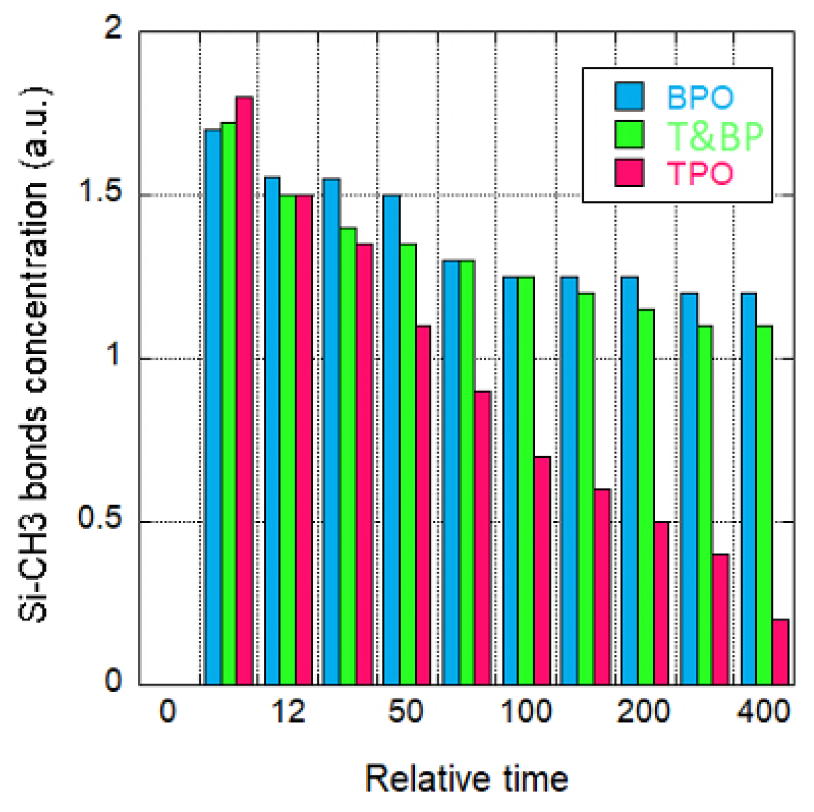
Modern plasma etch reactors provide the ability to control both the intensity of ion bombardment and the impact of active radicals. To better understand the individual contributions of these plasma components to plasma-induced damage, a series of experiments were conducted using an ICP plasma reactor [39]. Low-k films were treated under three different conditions:
  • Top Power Only (TPO)—generating plasma radicals without ion bombardment;
  • Bottom Power Only (BPO)—applying a bias to the bottom electrode, resulting in strong ion bombardment with minimal radical generation;
  • Top and Bottom Power (T&BP)—combining both plasma radicals and ion bombardment.
The exposure time in each condition was chosen to match the duration required to remove a specific thickness of photoresist (Figure 4). The results show that the reduction in Si–CH3 bonds (the 1275 cm−1 FTIR peak) under BPO and T&BP conditions is nearly the same and significantly lower than under TPO. This suggests that active radicals, particularly oxygen species, are primarily responsible for damaging the low-k films due to their ability to easily penetrate open pores. In contrast, ion bombardment in the BPO and T&BP conditions appears to partially seal the surface, thereby inhibiting the penetration of active radicals. Furthermore, the similarity in behavior between BPO and T&BP indicates that the efficiency of surface sealing by ion bombardment is independent of the presence of active radicals. It should be noted that the porous low-k films investigated in this work exhibited a porosity of 33% and a characteristic pore size of ~2.5 nm, as determined by ellipsometric porosimetry. The efficiency of surface sealing induced by ion bombardment is strongly dependent on both porosity and pore size (Figure 3).

2.3.3. VUV Damage

Plasma also emits vacuum ultraviolet (VUV) radiation, which possesses sufficient energy to break chemical bonds. VUV-induced damage to low-k materials has been extensively studied in the past, and significant insights have been gained through a variety of advanced characterization techniques. The most important findings have been reviewed and analyzed in Ref. [24]. The effects of VUV radiation can resemble those caused by chemical damage, though they are often more complex. The extent and depth of UV/VUV-induced damage strongly depend on the wavelength of the emitted photons. For example, when photon energy is below 6 eV, the damage is minimal. Maximum damage typically occurs in the 6–9 eV range. At higher photon energies, the degree of damage may decrease due to the high absorption coefficient of silica-based low-k materials, which limits light penetration depth.
VUV photons are capable of damaging even dense materials, although their absorption coefficients are influenced by the material’s density. Evidence of VUV-induced damage is apparent in the data presented in Figure 3 and Figure 4. In both cases, the depth of damage observed in films with porosities below the percolation threshold (Figure 3) and under ion bombardment (Figure 4) reaches several tens of nanometers. This is notably deeper than expected, given the limited penetration of active radicals in sub-threshold porosity films and the expected surface sealing from ion bombardment. These results suggest that the observed deeper damage may be attributed to the influence of VUV photons generated in the plasma. A more detailed analysis of these effects, including the synergistic interaction between active radicals and VUV photons, has been carried out using specialized gap experiments [41,42,43] and is thoroughly reviewed in the paper [7].
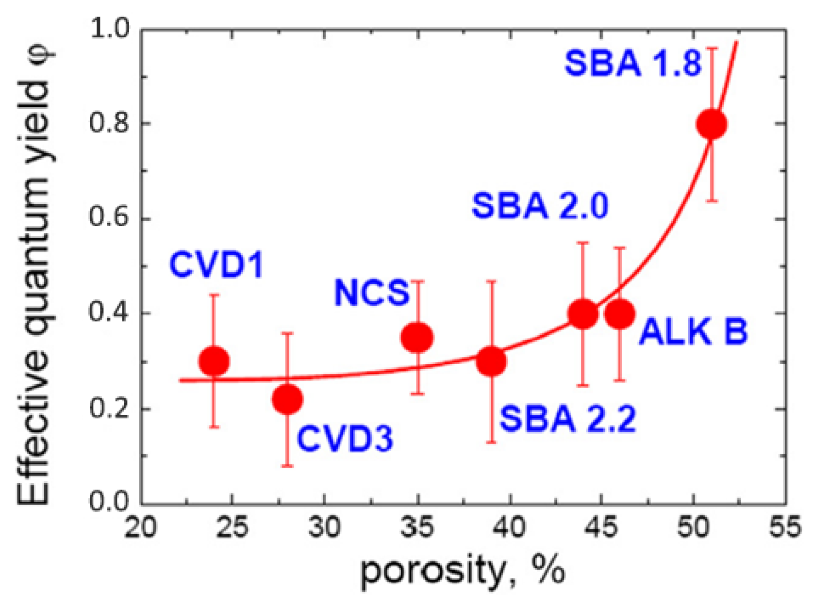
The data related to effect of porosity are limited. Rakhimova et al. [44] studied systematically effects of different wavelengths on low-k films with different porosity. In Figure 5, the effective quantum yield was calculated based on the VUV exposure results of the low-k dielectrics with porosity ranging from 20% to 55%. The effective quantum yield in the range between 0 and 1 quantifies the efficiency of CH3 escaping from the porous film with a possible reattachment of –CH3 back to dangling Si-bonds. For our opinion this dependence fairly correlating with percolation behavior is related to efficiency of removal of reaction products (CH3 radical) detached from the silicon atoms. They can be attached back during the diffusion through interconnected pores.
The electrical properties of low-k films are also strongly influenced by VUV exposure. Nichols et al. [45,46] reported that VUV irradiation decreases dielectric failure times and charge-to-breakdown in low-k dielectrics. In addition, VUV exposure can reduce leakage currents by promoting the decomposition of photoactive compounds [47]. In a manner analogous to UV curing. Conversely, other studies have shown that VUV photons generate additional defects and distorted bonds within the dielectric matrix. Similar increases in defect density and leakage current following UV irradiation have also been reported [48]. Sinha et al. [49] further suggested that photon irradiation produces trapped charges inside low-k materials, where such charge accumulation may pose long-term reliability concerns.

2.4. Concluding Remarks of Section 2

Low-k organosilica films developed for the interconnects of ULSI devices exhibit a complex structure. Materials with k ≥ 2.7–2.8 are typically deposited without sacrificial porogens, featuring constitutional porosity (<10%) and molecular-sized pores (0.5–1 nm). Films with k < 2.7 are deposited using sacrificial porogens, containing larger voids interconnected by narrow necks within the matrix. Both types of films demonstrate measurable diffusivity of neutral molecules such as toluene and isopropyl alcohol, as assessed by ellipsometric porosimetry. However, PALS reveals that first type films have non-interconnected pores, while more porous materials (>30% porosity) exhibit interconnected pores. The percolation threshold for positronium (Ps) is observed around 25%–30%, consistent with theoretical predictions for randomly embedded voids. The discrepancy between PALS and ellipsometric porosimetry data arises from Ps annihilation near pore walls and quantum mechanical constraints preventing Ps diffusion from large voids to narrow necks.
These characteristics are crucial for interpreting experimental results. For instance, the diffusion behavior of plasma-generated active radicals differs due to possibilities of recombination and interaction with pore walls. Furthermore, the depth of penetration depends on the nature of the radicals, as depicted in Figure 3. Therefore, understanding the percolation threshold measured by PALS is essential for assessing plasma damage. Additional efforts in process optimization, such as pore sealing, low-energy plasmas, and pulsed etching at sub-zero temperatures with pore-filling agents, are critical. Optimizing porosity and the chemistry of processing steps (e.g., hard masks, plasma conditions, repair layers) is crucial to maintaining film integrity while achieving desired k values. Techniques like pore stuffing (P4 approach) and cryogenic etching with micro-capillary condensation are also effective.
It is important to recognize that the percolation threshold exerts a substantial influence on both mechanical and electrical properties, including overall material reliability, as will be discussed in the following section. When analyzing the transport of various species, it is crucial to distinguish between the geometric and effective percolation thresholds. The geometric percolation threshold is intrinsic to the network structure and is independent of species lifetime. In contrast, the effective percolation threshold for species with finite lifetimes increases as the lifetime decreases. Consequently, in practical terms, percolation relevant to mass transport exhibits a clear dependence on species lifetime.

3. Percolation Phenomena Governing Electrical Failure in Low-k Films

3.1. General Overview of Percolation Phenomena in Porous OSG Low-k Films

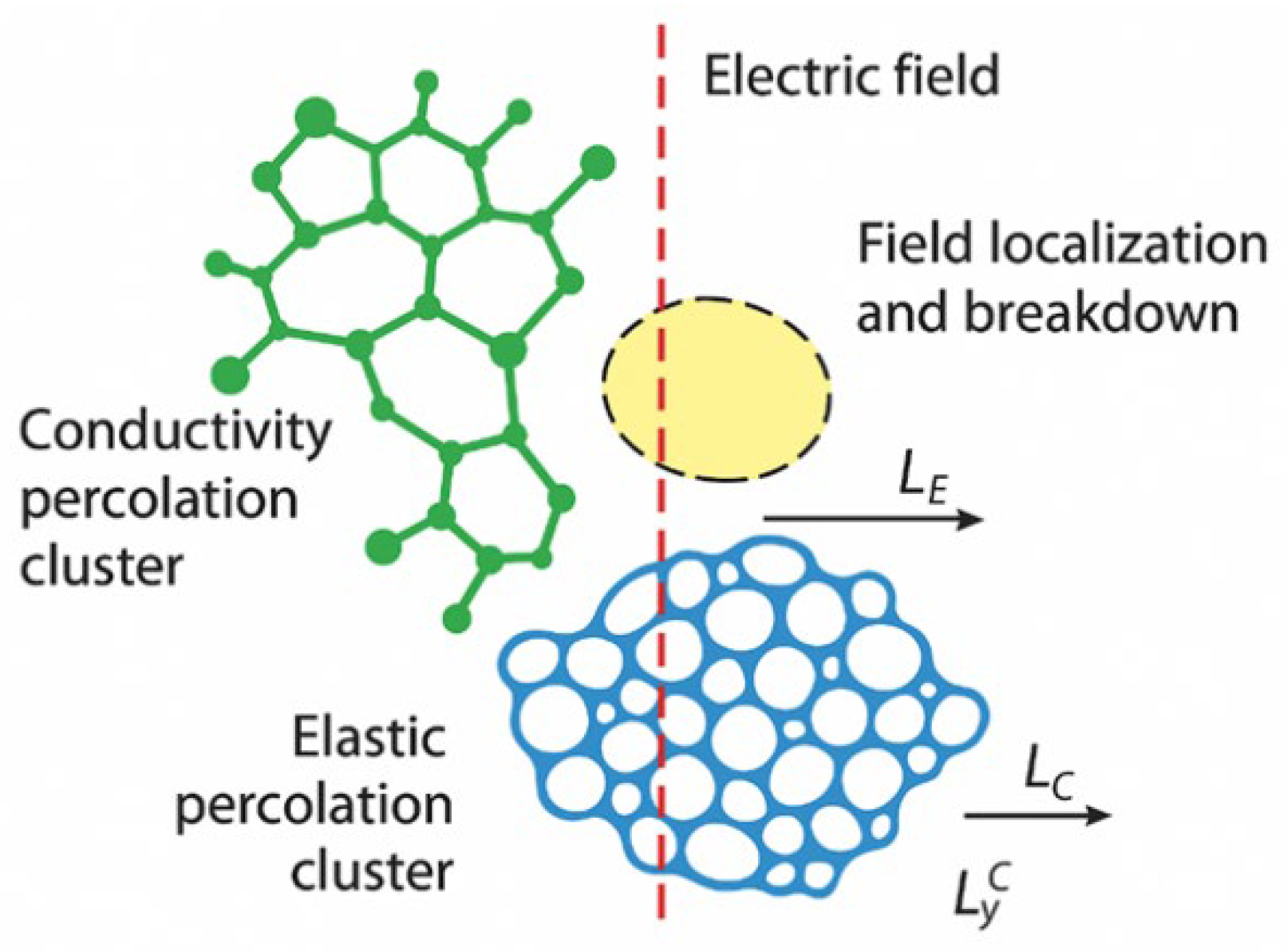
Percolation phenomena in porous OSG low-k dielectrics represent a critical bottleneck, where nanoscale porosity, introduced to achieve ultralow permittivity (k < 2.5), triggers catastrophic electrical failures when pore interconnectivity exceeds a critical porosity threshold pc (pc ~ 25%–30%). At this threshold point (Figure 6), isolated pore transition into percolating pathways that act as electrical short circuits, enabling rapid transport of charge carriers, moisture, and metal ions. These pathways drastically degrade dielectric integrity through three mechanisms: (i) breakdown voltage reduction by 40%–60%, as electric fields concentrate at pore/skeleton interfaces [50,51] (ii) exponential leakage current surges via Poole-Frenkel (PF) emission along defect chains [52]; and (iii) accelerated reliability failures as copper diffusion and moisture ingress propagate along connected pores, collapsing time-dependent dielectric breakdown (TDDB) lifetimes [53,54]. This threshold behavior is topologically deterministic, governed by pore morphology, defect density, and interfacial chemistry, making percolation a fundamental constraint in advanced interconnect scaling. To statistically quantify the failure risks arising from this percolative behavior, the Weibull distribution is widely employed. It models failure data such as TDDB using its shape parameter (β), which reflects the failure rate trend—for example, distinguishing between early-life, random, or wear-out failures.
Intrinsic material defects, such as graphitic sp2 carbon residues and oxygen vacancies—both originating from incomplete porogen (template) burnout—act as conductive nodes that seed percolation paths [55]. Extrinsic integration processes (like plasma etching, CMP) amplify damage by stripping hydrophobic methyl groups (–CH3), creating hydrophilic Si–OH bonds that adsorb moisture (k ≈ 80) [24]. This moisture enables ionic conduction via Grotthuss proton hopping [56] and facilitates copper migration, forming metallic filaments that bridge electrodes. Critically, the Weibull slope (β) of TDDB distributions flattens near the percolation threshold [51], reflecting heightened statistical dispersion in failure times due to stochastic defect clustering. Below 20 nm thicknesses, defect densities >1016 cm−3 guarantee percolation paths, rendering dielectric robustness irreversible [50,52]. Consequently, mitigation strategies must suppress porosity [57] and engineer network topology to delay percolation onset, as validated by cross-linked a-SiC:H films that maintain robustness at 40% porosity through optimized bond coordination [52].
Table 2 summarizes the trade-offs between dense and porous OSG films: while porous variants with lower k-values (<2.5), they suffer from 40% to 60% lower breakdown fields and compromised mechanical strength due to percolation-driven mass transport and plasma damage susceptibility. These weaknesses underscore the delicate balance between ultra-low permittivity and electrical reliability.
The details of percolation threshold and its influence on various properties of porous OSG low-k films are presented in Table 3.

3.1.1. Dielectric Constant and Leakage Current vs. Porosity and Chemical Composition

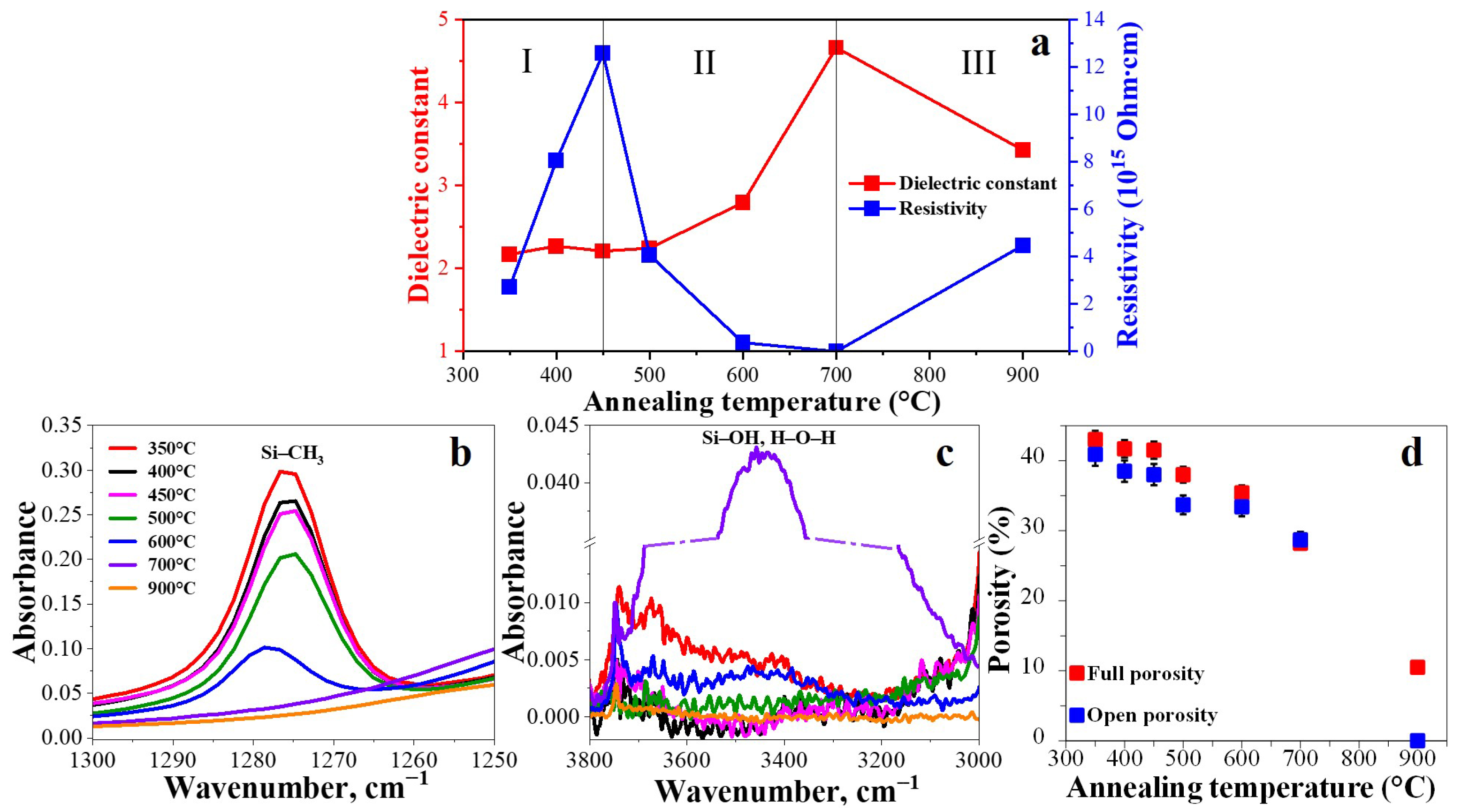
Figure 7 shows the variation in dielectric constant and leakage current (resistivity) of OSG low-k films (a) as a function of Si–CH3 concentration (b), adsorbed water concentration (c), and porosity (d), modified by annealing between 350 °C and 900 °C.
The first measurements were performed after annealing at 350 °C. According to FTIR data, the films annealed at this temperature were fully cured: the porogen was removed, and the porosity reached its maximum value. Therefore, any further changes observed during subsequent annealing are associated with gradual degradation of the film properties.
From the perspective of property evolution, the temperature range can be divided into three regions (Figure 7a):
  • 350 °C–450 °C.
The concentrations of Si–CH3 groups (b) and adsorbed water (c) remain almost unchanged, as does the porosity. This indicates that the low-k films are still stable in this range. However, a significant change in resistivity (leakage current) is observed, increasing from 2 × 10¹⁵ to 12 × 1015 Ω·cm. This change is attributed to the formation (at 350 °C) and gradual removal of template residues, likely sp2 carbon. Unfortunately, this residue is barely detectable in the FTIR spectra.
2.
450 °C–700 °C.
This range is characterized by a pronounced degradation of low-k properties: a strong reduction in Si–CH3 group concentration, an increase in adsorbed water content, and a marked decrease in porosity. These changes result in reduced resistivity and increased dielectric constant. The loss of Si–CH3 groups makes the films more hydrophilic, and the resulting moisture uptake further increases both leakage current and dielectric constant. Film densification in this range also contributes to the dielectric constant increase.
3.
700 °C–900 °C.
At both 700 °C and 900 °C, the Si–CH3 groups are completely removed, rendering the films highly hydrophilic. The highest amount of adsorbed moisture is observed in the films annealed at 700 °C. This elevated water uptake results in the lowest resistivity and highest dielectric constant among the studied samples. Annealing at 900 °C leads to a drastic reduction in porosity. Furthermore, the difference between open and closed porosity increases, suggesting that micropore collapse causes some pores to become closed. Consequently, these closed pores are inaccessible to water molecules, as confirmed by FTIR, and the total amount of adsorbed moisture decreases significantly. This reduction in water content leads to a decrease in the dielectric constant and an increase in resistivity compared to the 700 °C samples.
Effect of hydrocarbon residues adsorbed from contaminated UV curing chamber has been studied (Figure 8). The low-k sample (spin-on deposited OSG films with 40% porosity, Figure 8d) was loaded into a vacuum chamber pumped by a dry turbomolecular pump. Both porosity (Figure 8d) and leakage current (Figure 8a) remained unchanged when the sample was kept in the chamber purged with nitrogen. However, the film’s porosity decreased from 40% to 29% when the same sample was placed in the vacuum chamber without nitrogen purge. Correspondingly, the FTIR spectra showed a significant increase in hydrocarbon concentration (Figure 8b), along with an increase in leakage current (Figure 8a). Part of the adsorbed hydrocarbons was weakly bonded to pore wall and could be easily removed by nitrogen purging at 250 °C. Much stronger accumulation of hydrocarbon residues and a further increase in leakage current were observed when the sample in this vacuum chamber was exposed to VUV light (180 nm). This pronounced accumulation of hydrocarbon residues is most likely due to photoinduced desorption of hydrocarbons from the chamber walls, which increases their concentration in the gas phase and leads to their subsequent re-adsorption into the low-k film.
Nitrogen purging during VUV exposure reduced the amount of adsorbed hydrocarbons and increased the open porosity. However, the leakage current has increased even further compared to vacuum exposure alone. These phenomena can be explained by photochemical reactions, given that the photon energy of 180 nm light (6.9 eV) is sufficient to break C–H (4.3 eV) and C–C (3.6 eV) bonds in hydrocarbon films, thereby converting some residues into graphitic sp2 carbon clusters and unsaturated carbon sites. These species have higher electrical conductivity and can form percolation pathways. Additionally, VUV photons can cause photoemission or excite electrons into the conduction band of the material or substrate. The resulting ionized carbon sites act as deep or shallow traps. Under an applied bias, carriers can hop or tunnel between these traps—a mechanism known as trap-assisted conduction—which manifests as increased leakage current [59,60]. In experiments involving nitrogen, VUV photons can dissociate N2 into metastable N* species that react with radicals in the hydrocarbon film, forming C–N bonds or nitrides. However, 180 nm photons cannot effectively dissociate N2 directly, but CH radicals or other hydrocarbon-derived intermediates may activate N2 and incorporate nitrogen into C–N bonds via indirect photochemical pathways. This interaction can modify trap density and conduction pathways. Some studies have shown that N2/VUV exposure promotes nitrogen doping of carbon surfaces, altering their conductivity.
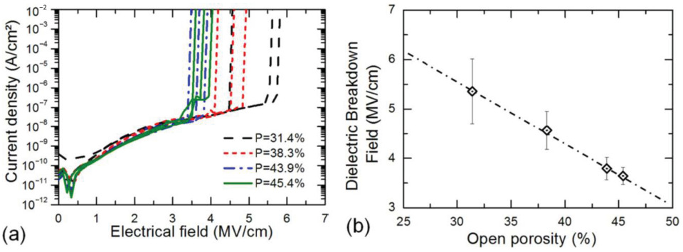
The data presented in Figure 7 and Figure 8 suggest that increase in leakage current most probably related to impact of surface compounds formed on pore walls and groups that can form percolative passes when pore are fully interconnected. To prove this statement, it would be interesting to study OSG films free on surface compounds. Vanstreels et al. reported such data [61] for porogen-residue-free, highly hydrophobic films prepared using a specialized fabrication process [62]. In these films, with porosity ranging from 30% to 50%, the leakage current was found to be independent of porosity, suggesting that in residue-free films the pore wall surface no longer plays a dominant role (Figure 9). Instead, the leakage current seems to be governed by other factors—possibly including the presence of oxygen-deficient centers (ODCs)—and is significantly lower than in conventional porogen-residue-containing or hydrophilic OSG films. In contrast, the breakdown field remains dependent on porosity (Figure 9b), decreasing approximately linearly with increasing porosity.
In contrast, higher porosity lowered the breakdown voltage—from 6 MV/cm at 31% porosity to 3.5 MV/cm at 44%–45%—due to fewer cage structures, increased Si–O–Si backbone strain under electric fields, and local field intensification near pores.
Leakage currents in porous OSG low-k dielectrics exhibit distinct behavior governed by porosity-dependent conduction mechanisms. Below the critical porosity threshold (pc ≈ 25%–35%), leakage is dominated by localized charge transport processes such as trap-assisted tunneling and PF emission [52,63,64]. Isolated pores (Figure 6a) create localized electric field enhancements at pore/skeleton interfaces due to permittivity contrast (kpore ≈ 1 vs. kmatrix ∼ 3–4), but the dielectric matrix constrains long-range charge movement [63]. Electrons primarily hop between intrinsic defects (oxygen vacancies, strained Si–C bonds) and extrinsic traps (e.g., graphitic carbon residues from incomplete porogen burnout), with leakage scaling moderately with field strength via PF emission [65].
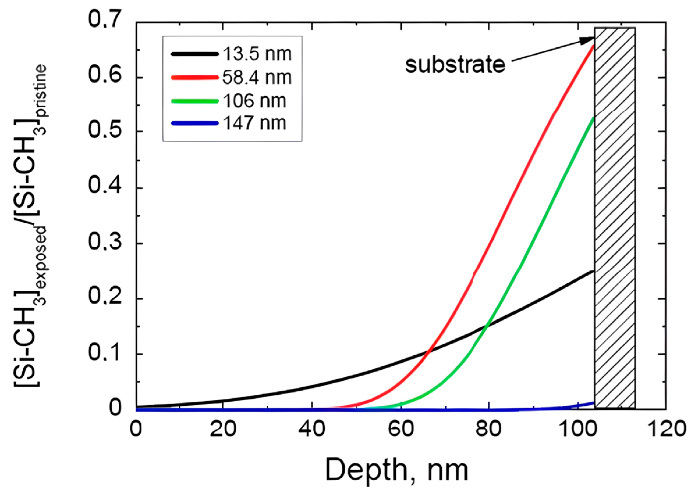
Trap-assisted conduction in low-k dielectrics originates from electronic traps, localized states within the bandgap, created by synergistic intrinsic defects and extrinsic plasma damage. Chemical imperfections like strained Si–C bonds, hydrophilic Si–OH groups (from moisture access), and non-bridging oxygen radicals (Si–O•) generate deep-level traps (>3 eV below conduction band) that capture electrons [52,57]. These defects are catastrophically amplified by plasma processing: for instance, VUV photons (147 nm) generated in Xe plasma penetrate porous networks, severing hydrophobic Si–CH3 bonds and leaving carbon dangling bonds (•C) and oxygen vacancies (≡Si•) as shallow traps near the conduction band. Figure 10 [66] quantifies this damage, showing 147 nm light depletes 80% of Si–CH3 bonds in high-porosity films, with defect density peaking at the dielectric interface. The degree and depth of UV damage depends on wavelength. Critically, isolated traps remain electrically benign until exceeding a threshold density (~1016 cm−3), where overlapping wavefunctions enable trap-to-trap tunneling. Beyond this point, accelerated at porosities >30% where pores concentrate defects, traps aggregate into conductive filaments via percolation [50]. This transition is stochastic but topologically inevitable where pore connectivity reduces the critical defect separation to <1 nm, allowing electrons to hop along chains spanning electrodes [51].

3.1.2. Leakage Current in Porous Low-k Films and Reliability

The reliability consequences manifest in real-time leakage evolution (Figure 11) and statistical failure shifts. Leakage currents surge exponentially as defect chains lower activation barriers for PF emission; electrons hop between traps with barrier reduction Δφ ∝ √E. Residue-rich films (sp2 carbon clusters) exhibit 1000× higher leakage at 3 MV/cm than clean matrices [67]. Simultaneously, breakdown strength collapses by 40%–60% and electric fields intensify to >4× applied levels at trap-rich pore interfaces [68], exceeding Si–O bond strength (8–10 eV) and triggering cascading bond breakage.
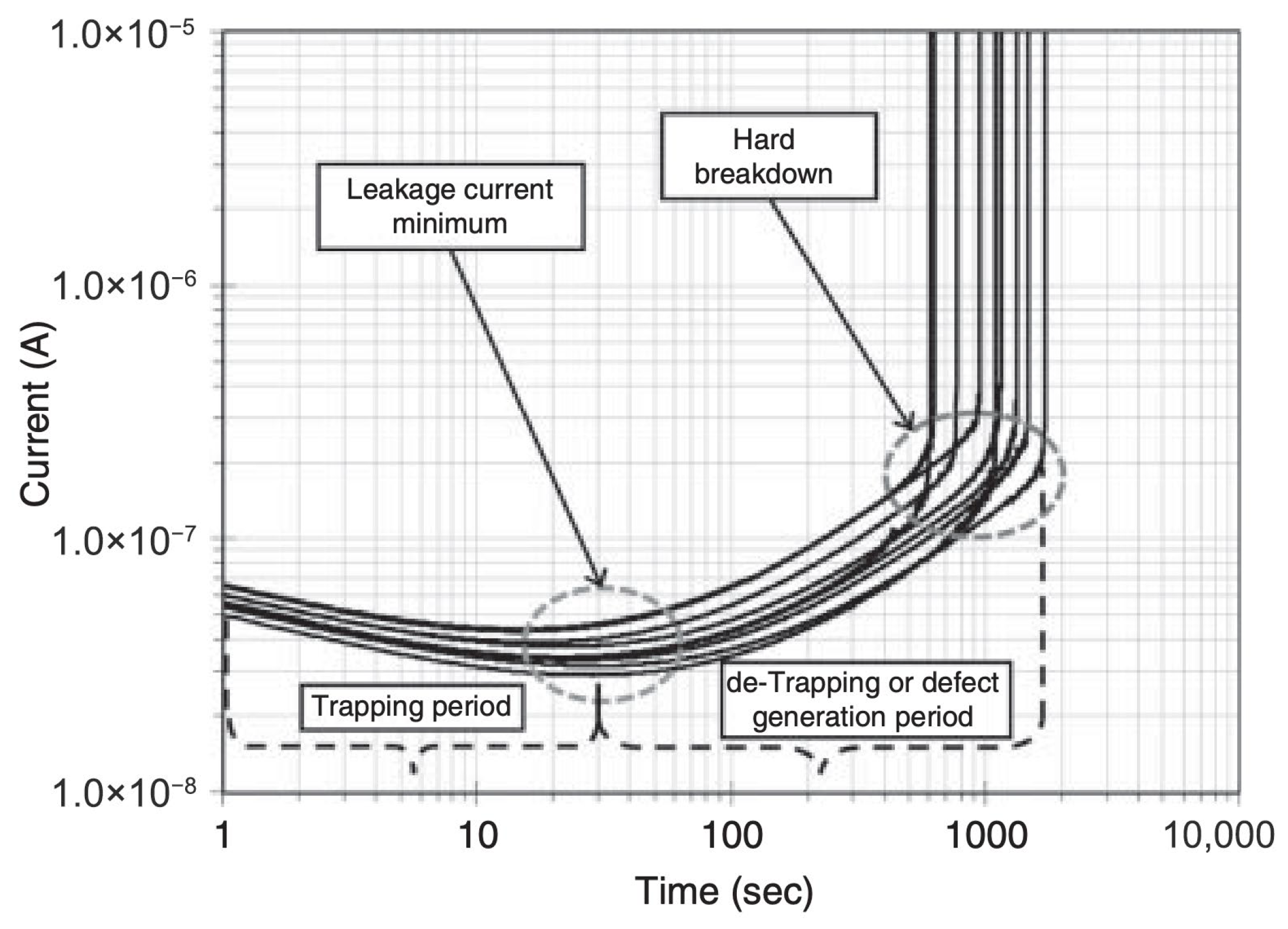
Figure 11 captures this progression: phase I shows current decrease as traps fill; phase II reveals gradual current rise from new defect generation (Cu+ drift along hydrated pores); phase III marks abrupt hard breakdown when percolation paths bridge electrodes. This aligns with flattened Weibull slopes (β < 2 vs. β > 5 in dense films), reflecting unpredictable early failures [51]. Plasma damage creates a malicious cycle: each etch step generates fresh traps that interconnect existing chains [52].
At the percolation threshold (ppc), isolated pores interconnect into continuous pathways, triggering an abrupt, exponential surge in leakage (Figure 6c) [52,63]. This transition enables percolative conduction, where charges bypass the matrix via low-resistance tunnels formed by connected pores or defect chains [64,65]. Simulations of failure distributions confirm that electric fields intensify by >4× at pore necks (4.5 MV/cm locally vs. 3.3 MV/cm applied) [64], accelerating charge injection. Moisture exacerbates this effect: hydrophilic Si–OH bonds (from plasma damage) adsorb water, dissociating into H3O+/OH ions that enable ionic conduction via Grotthuss proton hopping [69]. This transforms pores into proton highways, elevating leakage by 10–100× in humid environments [70].
Moisture and ionic contaminants (Na+, K+, Cl) exploit porous networks in low-k dielectrics, migrating through interconnected pores and transforming inert voids into conductive pathways. Plasma-induced hydrophilicity, caused by methyl group (–CH3) depletion (Figure 10), creates hydrophilic Si–OH surfaces that chemisorb water monolayers, while capillary action draws additional moisture deeper into the film [52]. Under elevated temperature and humidity, this adsorbed water dissociates into H3O+ and OH ions, enabling ionic conduction through Grotthuss proton-hopping along hydrogen-bonded networks [69]. Simultaneously, the dissolved ions (Cl from etch residues) migrate under bias, creating electrolytic currents that scale with pore connectivity. Critically, moisture amplifies pre-existing trap-assisted paths where water molecules passivate deep traps (Si–O•) but generate shallow proton traps (Si–OH2+), lowering activation barriers for PF emission by up to 0.5 eV [70]. This synergy is self-propagating, humid environments accelerate Cu2+ diffusion along hydrated interfaces, depositing metallic clusters that further enhance local fields [71].
The reliability impacts are severe and multifaceted. Leakage currents surge by 10–100× in humid conditions, exhibiting nonlinear JE curves with characteristic humps at 1–2 MV/cm [72], a signature of ionic hopping transitions. More critically, moisture reduces breakdown fields by 30%–50% through dual mechanisms: (i) the high permittivity of water (k ≈ 80) concentrates electric fields at pore interfaces, exceeding the intrinsic breakdown strength (8–10 eV) and triggering Si–O bond rupture [68]; (ii) the hydrated Cu ions form dendritic filaments along percolation paths, bridging electrodes at lower voltage [53]. TDDB lifetimes collapse exponentially with humidity, chemisorbed water (requiring >400 °C annealing for removal) increases the thermal activation energy of breakdown by 0.7 eV, while hydrophilicity flattens Weibull slopes (β) to <2 [65].
Conductive residues further amplify leakage. Graphitic sp2 carbon clusters, trapped during non-optimized porogen burnout, act as ohmic paths with resistivity ∼10−3 Ω∙cm, independent of electric field [67]. These residues lower PF activation barriers by up to 0.5 eV and enable direct tunneling at high fields (>3 MV/cm) [73]. Plasma processing (RIE and ashing) deposits conductive carbon residues on the pores wall, primarily graphitic sp2 clusters, which are formed by the incomplete combustion of organic porogens or photoresists. These residues, accumulating at pore necks and interfaces, create ohmic conduction paths independent of electric field. Wu et al. [52] quantified leakage increases of 10–100× in films with >20% carbon residue coverage, as electrons bypass the dielectric matrix via these low-resistance filaments (resistivity ~10−3 Ω∙cm). Critically, carbon residues synergize with trap-assisted conduction where sp2 sites act as deep traps that capture charges, enhancing PF emission at low fields (<1 MV/cm), while enabling direct tunneling at high fields. This dual mechanism is worsened by pore connectivity, residues at interconnected pore junctions form conductive bridges that override the Pc at lower defect densities [50]. Similarly, the barrier layer damage during integration further injects metallic particles (Cu, Ta) into the dielectric. Therefore, the metallic contaminants for like Cu, Ta diffuse along hydrated pores during integration, precipitating as nanoclusters (<5 nm) that intensify local fields (Figure 12) [53]. Plasma etching residues or barrier-layer damage inject these metals, creating preferential percolation paths that reduce the critical defect density for conduction by 3× compared to pristine pores [50].
The reliability impact is severe. Above pc, leakage currents surge exponentially, governed by interconnected defect networks rather than bulk properties [51]. This erodes dielectric integrity, accelerating TDDB and flattening Weibull slopes (β < 2) [74]. Plasma processes worsen this by expanding pores >50% and generating fresh traps (carbon dangling bonds), which interconnect existing chains [44]. Plasma processing (etching, ashing) actively reshapes pore networks through radical-driven restructuring. Reactive species (O•, H•, CFx•) penetrate interconnected pores, scouring pore walls and severing Si–CH3 bonds. This not only generates carbon dangling bonds (trap sites) but etches the matrix backbone, expanding pore diameters by >50% and merging isolated voids into continuous channels [44]. The resulting pore connectivity surge transforms the dielectric into a percolated network, effectively predetermining conduction paths before voltage application. Moisture exacerbates this where plasma-created Si–OH groups adsorb water, which reacts with radicals to form corrosive acids (HF from F•), accelerating matrix dissolution. Critically, 147 nm VUV photons [44] inflict deepest damage due to low absorption in OSG, enabling uniform restructuring through thick films. These plasma-expanded channels act as low-resistance highways, facilitating rapid diffusion of contaminants and lowering activation barriers for ionic conduction.
Plasma-expanded pores catastrophically degrade dielectric integrity. Leakage currents increase due to: (i) ohmic transport through connected pores; (ii) enhanced trap-assisted tunneling along damaged walls; and (iii) electrolytic currents from moisture ingress. Simultaneously, breakdown fields plummet by 40%–60% as enlarged pores intensify local electric fields and reduce the effective dielectric thickness [51]. Figure 12 quantifies this vulnerability: high-porosity films (50%) exhibit near-unity quantum yield for bond breakage, meaning almost every photon creates a defect. This damage flattens TDDB Weibull slopes to β < 1.5 (vs. β > 5 in pristine films), indicating stochastic early failures [51]. Crucially, the plasma damage creates irreversible percolation seeds when ALD barrier precursors penetrate the expanded pores and depositing conductive Ta clusters that further elevate leakage.

3.1.3. Breakdown Voltage

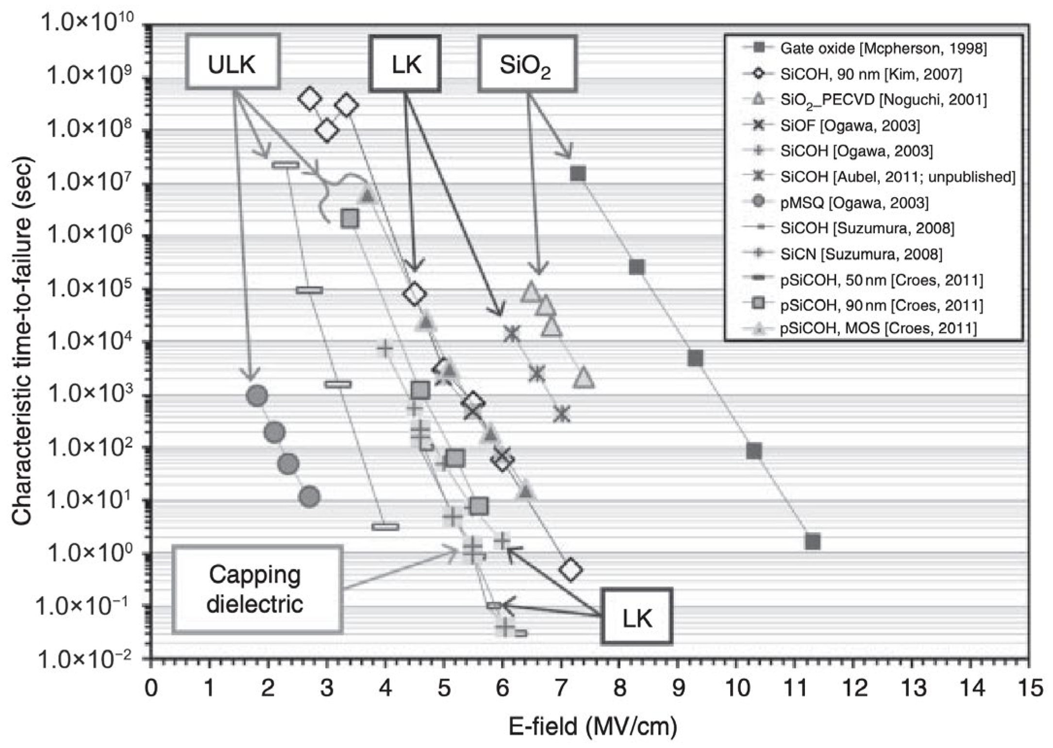
Some studies have analyzed local electric field enhancements caused by porosity and their effect on the probability of breakdown, and have also discussed possible mechanisms, including the presence of moisture and active centers in the band gap [50,63,73]. Ogawa et al. [75] considered the pore as a pre-existing defect and using a percolation model to predict relative breakdown fields. They demonstrated that porosity in SiO2 films has virtually no effect on the physics of breakdown but significantly influences the time to breakdown (TDDB). In this study, pores were considered as pre-existing defects that make it easier for conductive paths to form in dielectric material. The key conclusion is that porosity does not really affect the fundamental physical processes that determine the mechanism of electrical breakdown. Nevertheless, the presence of pores significantly reduces the time to breakdown, which manifests itself in a decrease in the shape parameter (β) of the Weibull distribution. The decrease in β, in turn, is due to an increase in the statistical variability of breakdown paths, which is a direct consequence of the percolation nature of the formation of conductive channels. Thus, porosity contributes to the formation of multiple alternative paths for breakdown, thereby increasing the dispersion in the distribution of failure times. Ogawa et al. [63] also investigated the effect of porosity on leakage currents, breakdown, and time to dielectric breakdown (TDDB) in various low-k silicon-based dielectrics, including fluorinated silica (FSG), porous carbon-doped silica (OSG), and highly porous methylsilsequioxane (P-MSQ). Experimental data demonstrate that an increase in porosity (resulting in a decrease in the dielectric constant k, to 2.1–2.3) leads to a significant reduction in breakdown voltage EBD (from ~10 for CVD-SiO2 to ~4 mV/cm for P-MSQ). Additionally, it reduces the time to breakdown, while the breakdown kinetics (field acceleration parameter γ ≈ 4.5 cm/mV and activation energy Ea ≈ 0.5–0.66 eV) remain unchanged.
In [76], Hong et al. used modeling to show that pores can cause local field enhancement in porous low-k films, and that high-field regions around pores can create an effective conduction path for drifting charged particles, accelerating dielectric breakdown. In addition, the work [77] also demonstrated the calculation in the COMSOL environment in porous SiO2 (porosity 30%) showing that the local field around the pores increases significantly. It was found that the combined effect of an increase in the electric field at the pore edges and a decrease in the activation energy of diffusion leads to a reduction in the time to breakdown by 26% for a relatively dense material.
It was also reported in [53,78] that the drift of Cu ions at the cap/low-k boundary is the dominant factor causing dielectric breakdown. The dielectric breakdown is associated with a critical copper concentration in the dielectric, and this concentration depends on the current conduction mechanism, i.e., Schottky or Poole-Frenkel. Since the field dependence in both conduction mechanisms is the square root of the electric field, the failure time has a √E dependence. Lloyd et al. [69] reported that the presence of Cu was not a necessary condition for failure, but its presence significantly reduced the failure time. In all the above models, the role of pores and copper in low-k dielectric breakdown is considered separately, so the physics of breakdown is still unclear. An extension of the Ogawa model was made in [50], where porosity and copper ions were taken into account. The colleagues showed (simulation in the Ansys environment) that a local maximum field (Emax) will arise inside the pore and will propagate perpendicular to the applied electric field (Figure 12). The maximum field was 4.5 MV/cm, which is about 1.4 times higher than the applied average field (3.3 MV/cm). This is because the electric flux is concentrated around the pores due to the low dielectric constant of the pores (k = 1).
By comparing the simulation results of the local field enhancement of pores and Cu clusters [77], it was shown that Cu clusters have a stronger field enhancement effect than pores, which significantly worsens the reliability of the dielectric under stress conditions. But under the use condition, although the ratio of Emax/Eave is the same as under stress conditions, the difference in the absolute field value between pores and Cu clusters becomes small, and therefore its effect on the failure time of the dielectric becomes less important. Therefore, it is necessary to consider the field enhancement due to pores in the reliability characterization of porous low-k dielectrics. In fact, the field enhancement due to pores is equivalent to shortening the percolation path (or dielectric thickness) for breakdown, which did not change the physics of dielectric breakdown, but would significantly affect the failure time of the dielectric.
Figure 13 [74] plots the maximum allowed electric field (Emax) versus porosity for 20–60 nm films, showing how Emax decays exponentially as porosity rises. This summarizes the percolation-driven erosion of dielectric robustness and underscores the thickness-porosity interdependence critical for reliability modeling. Including the H2 treatment’s impact on reducing intrinsic defects provides context for why some high-porosity films might outperform expectations.
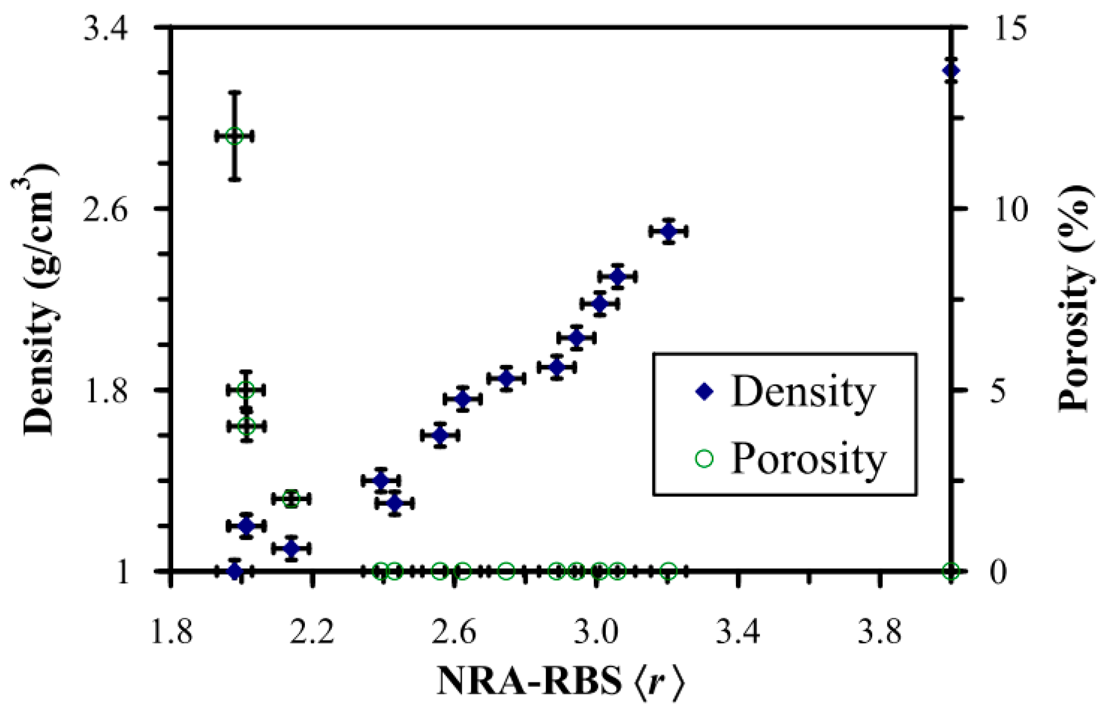
Based on the King et al. [57] study, the influence of network bond percolation on electrical failure and reliability in low-k a-SiC:H films reveal a critical relationship with the average coordination number, ⟨r⟩. Electrical resistivity exhibits a distinct saturation behavior as ⟨r⟩ decreases. Specifically, resistivity increases significantly with reduced network connectivity but plateaus near ⟨r⟩ ≈ 2.4–2.5, slightly above the rigidity percolation threshold (⟨rc = 2.4) observed for mechanical properties. This saturation is attributed to conduction transitioning to a site-percolation mechanism governed by electron transport between point defects or traps in the dielectric bandgap. The dominant mechanism is Frenkel-Poole (FP) conduction, where the applied electric field lowers the energy barrier for trapped electrons to hop between defect sites. The authors note that the observed critical point (⟨r⟩ ≈ 2.5) aligns more closely with site-percolation theory (predicted ⟨rc = 2.3) than bond-percolation models (⟨rc = 2.4), likely due to the additional energy constraints inherent to FP conduction.
From a reliability perspective, reducing ⟨r⟩ to achieve lower-k involves inherent issues. While lower ⟨r⟩ increases resistivity (beneficial for leakage reduction), it simultaneously compromises mechanical and thermal properties, creating vulnerabilities for device failure. Below ⟨r⟩c ≈ 2.4, interconnected nano-porosity percolates (Figure 14), causing abrupt deteriorations in thermal conductivity and potentially accelerating dielectric breakdown under thermal stress.
Furthermore, the films near ⟨r⟩c exhibit homopolar bonding shifts (Si–Si, C–C) and increased terminal groups, which may introduce electronic traps that exacerbate leakage under bias. They concluded that while reduced connectivity below ⟨r⟩c theoretically stabilizes elastic properties, pore percolation and defect-dominated conduction pose significant reliability risks, highlighting the challenge in balancing ultra-low k targets with robust electrical performance. Strategic design, such as incorporating deformable C–C–C chains or stiff, low-polarizability bonds, is suggested to mitigate these issues.
Paquette et al. [79] highlights how percolation theory governs key electrical transitions in amorphous semiconductors and dielectrics. In crystalline and amorphous semiconductors, increasing dopant concentration beyond a critical threshold (Nc) triggers a metal-insulator transition. Below Nc, dopant states are localized and conductivity is suppressed, but at Nc, these states delocalize to form percolating paths, enabling metallic conduction. This transition follows a universal scaling law: σ(0) = σ0[(NNc)/Nc]ν, where ν is a critical exponent. Interestingly, this mirrors the mechanical rigidity percolation transition described by Phillips-Thorpe theory, with dopant concentration (N) analogous to mean coordination number (⟨r⟩). Such transitions underpin emerging resistance-switching devices, where voltage-controlled percolation paths enable novel memory and logic functionalities.
In amorphous dielectrics, electrical percolation thresholds manifest through mean network coordination (⟨r⟩). For example, in hydrogenated amorphous silicon carbide (a-SiC:H), resistivity increases as hydrogen (acting as a network modifier) reduces ⟨r⟩, eventually plateauing near ⟨r⟩ = 2.4. This aligns perfectly with the critical coordination predicted for conductivity percolation in tetrahedral resistor networks, where resistor bonds below ∼39% density halt current flow. Similar plateaus in resistivity occur in hydrogenated boron carbide (a-Bx C:H) at 30–35% H content, further underscoring the role of topological constraints. Crucially, reducing ⟨r⟩ also lowers dielectric constant (k) in organosilicate low-k dielectrics, but simultaneously weakens mechanical properties, creating a fundamental issue governed by percolation-driven rigidity loss.
The percolation model conceptualizes the low-k dielectric as a composite where pores (k = 1) act as intrinsic defects within the silica matrix. The critical percolation threshold is reached when pore density and connectivity enable a continuous conductive pathway. Figure 15 starkly demonstrates this threshold effect experimentally: as k-values decrease below ~2.7 (signifying increased porosity), the characteristic breakdown field (EBD) plummets and the Weibull shape factor (β) worsens.
This confirms that porosity does not just linearly degrade properties but triggers a nonlinear collapse in intrinsic robustness near a material-specific threshold. Hyper-porous ULKs (k < 2.3) and ELK materials (k ≤ 2.0) operate perilously close to this threshold, where even minor process variations (ash damage, moisture uptake) or inherent pore connectivity can catastrophically reduce the number of defects needed to form a lethal percolation path. The model explains why these materials show such poor Weibull β values—broader failure distributions reflect the heightened statistical variability in forming critical defect clusters within the porous network.
Modeling and experimental validation: Percolation modeling resolves key conflicts in lifetime extrapolation. While traditional models (E-model, √E-model) debate field dependence, percolation provides the physical basis for observed trends (i) Area scaling: The consistent Weibull statistics (validated by Figure 11.10 and area-scaling relationships like Equation 11.4 in Ogawa et al. [50]) confirm percolation as a weakest-link mechanism. Larger areas contain more potential critical defect clusters, accelerating failure, (ii) k-value dependency: Figure 15 compiles experimental proof that breakdown strength collapses as k decreases. The percolation model attributes this to higher porosity increasing defect density (pores) and reducing the inter-defect spacing, easing conductive path formation and (iii) Pore structure role: The model emphasizes that not just porosity %, but pore size distribution and connectivity (open vs. closed pores) dictate percolation susceptibility. This explains why identical k-values from different processes show divergent reliability, pore topology matters critically.
Percolation theory thus transforms low-k reliability from a mere integration challenge into a fundamental materials science problem governed by defect statistics and network connectivity, with profound implications for future technology scaling.
In summary, the percolation phenomena govern catastrophic electrical failures in OSG-based low-k dielectrics, where nanoscale porosity, introduced to achieve k < 2.5, transforms from isolated voids into interconnected conduction paths once exceeding a critical threshold (25%–30% porosity). This percolation transition enables five key failure mechanisms: (i) trap-assisted conduction along defect chains (Si–OH, sp2 carbon); (ii) moisture-induced ionic transport through hydrated pores; (iii) ohmic leakage via carbon/metallic residues (Cu, Ta); (iv) plasma-expanded pore networks acting as low-resistance highways; and (v) electrical aging dynamically generating percolation paths under bias. Beyond the threshold, leakage currents surge exponentially, breakdown voltages drop by 40%–60%, and TDDB lifetimes collapse as stochastic percolation paths bridge electrodes, flattening Weibull slopes (β < 2) and eroding reliability.
Mitigation strategies disrupt percolation physics by elevating the critical threshold:
  • Material design: Optimizing network topology via cross-linking (Si–O–Si rings in a-SiC:H) delays pore interconnectivity beyond 40% porosity [57], while H2/He plasmas remove sp2 carbon residues [62,67].
  • Surface engineering: Hydrophobic SAMs seal pore entrances, blocking moisture/contaminant ingress [80], while size-excluded ALD precursors prevent metal diffusion [81].
  • Integration control: Pore stuffing (P4 approach) with pore protection by deposited polymers [82,83] and cryogenic etching (−100 °C), which condenses byproducts to minimize plasma damage [84], silylation passivates Si–OH traps, and stress-graded porosity design weakens field enhancement by 30%–50% [79]. These approaches collectively shift the percolation threshold, suppress defect connectivity, and restore dielectric robustness even at ULK regimes.

4. Mechanical Properties of Porous Low-k Materials

The mechanical properties of low-k films are critical to the successful integration of ULSI interconnects, as the films must withstand both the full manufacturing sequence and long-term operational conditions. Parameters such as elastic modulus, hardness, adhesion strength, and fracture toughness govern the ability of a low-k film to resist cracking, delamination, or degradation of dielectric performance during fabrication, packaging, and service. Insufficient mechanical robustness can offset the electrical advantages provided by low permittivity [85].

4.1. Mechanical Properties Versus Connectivity and Porosity

Table 4 summarizes the relationship between the mechanical properties of low-k films and ULSI requirements, associated metrics, and typical failure modes.
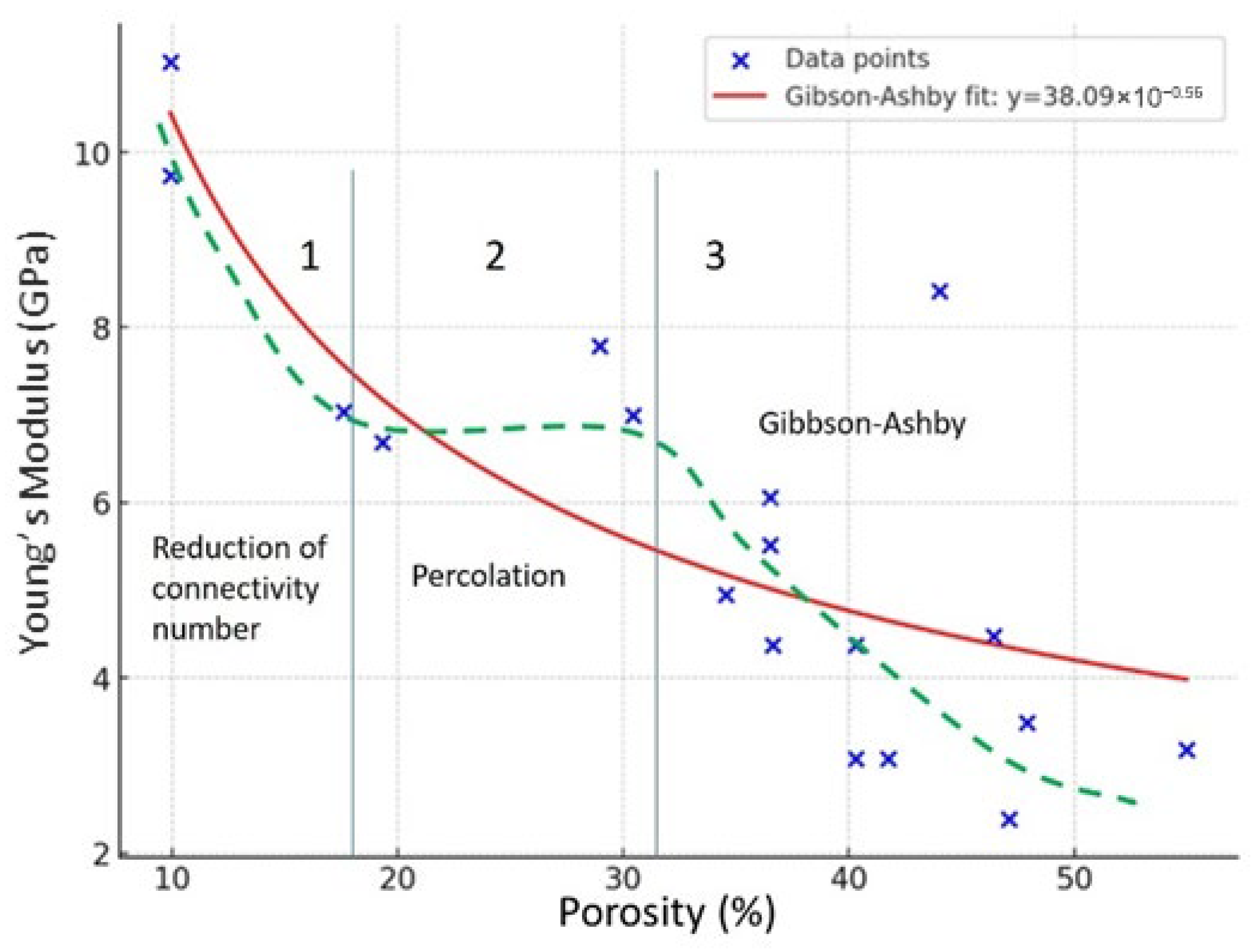
Table 4 demonstrates that integrated low-k materials exhibit diverse mechanical property requirements, which are primarily dictated by porosity. The present work reviews the relationship between Young’s modulus and porosity in the investigated films, with particular emphasis on issues associated with the percolation threshold. In porous low-k dielectrics, the Young’s modulus (E) decreases markedly with increasing porosity, as pores simultaneously reduce the fraction of load-bearing solid material and serve as stress concentrators.
Experimental studies of porosity effects in nanoporous low-k dielectrics are often complicated by the difficulty of disentangling porosity from intrinsic matrix properties. In organosilicate glass (OSG) thin films prepared using the porogen approach, porosity is controlled by adjusting the porogen loading during deposition. Removal of the porogen phase typically requires post-deposition treatments such as annealing or ultraviolet (UV)-assisted curing. Because the matrix bond network is highly sensitive to the specific conditions of UV irradiation, the porogen-removal process can modify the matrix structure to varying degrees, depending on the initial porogen content [23].

4.1.1. Mechanical Properties Versus the Matrix Connectivity (Dense OSG)

In comparing the mechanical properties of OSG low-k dielectrics with those of SiO2, the observed reduction in mechanical strength is primarily attributed to the substitution of bridging oxygen atoms with terminal methyl groups, which decreases the overall network connectivity. This effect is rationalized within the framework of Phillips–Thorpe constraint theory, which correlates the mechanical rigidity of glass networks with the number of topological constraints (bond-stretching and bond-bending interactions) relative to the available atomic degrees of freedom [86]. This theory was first applied to OSG low-k films by Gleason and co-workers, who provided a physical explanation of the percolation effect arising from changes in bond connectivity during film fabrication and its consequent influence on the mechanical properties of organosilicate glass dielectrics. [87,88].
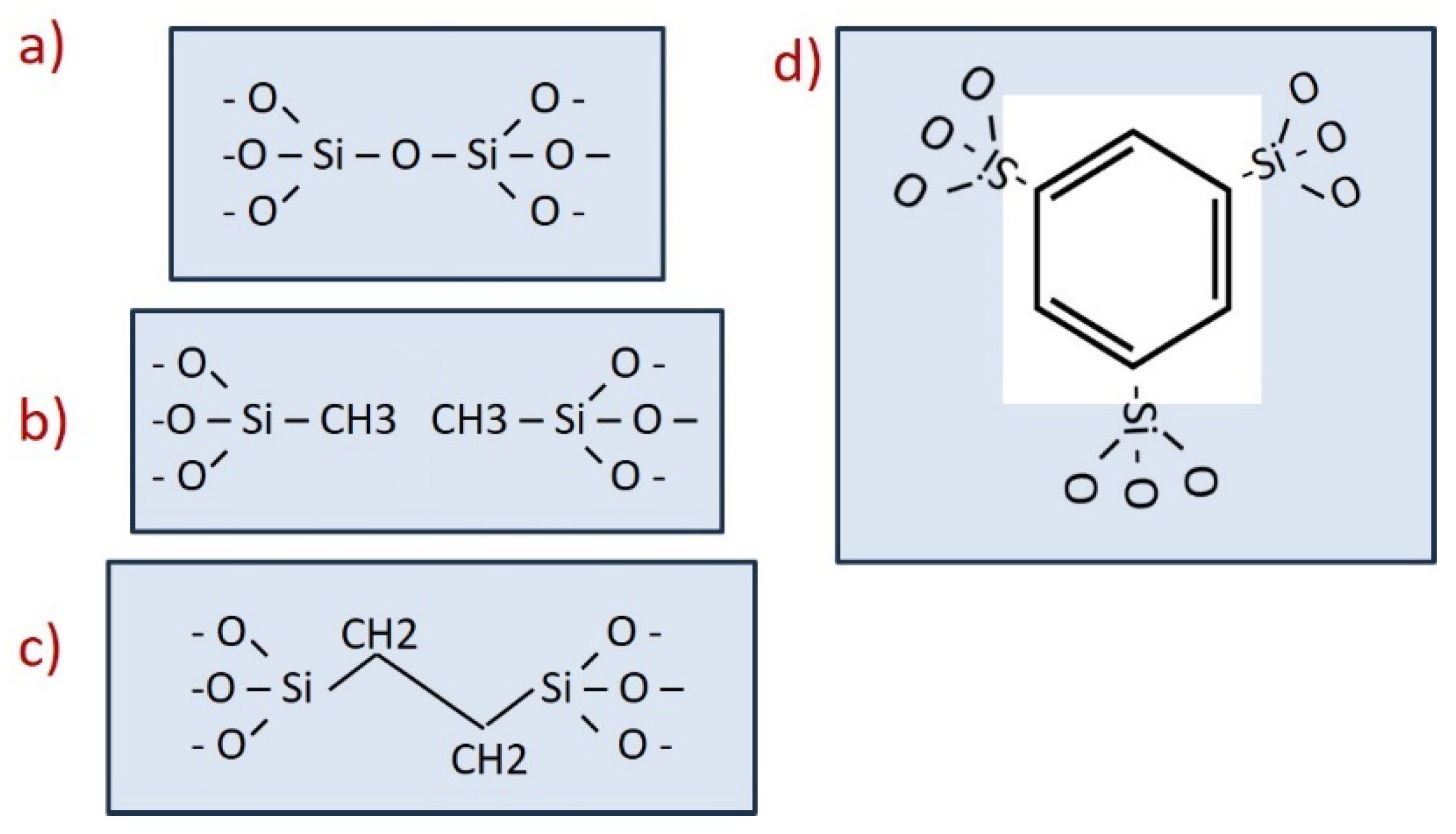
In their model, the reduction in Young’s modulus arises from the breaking of bridging (Si–O–Si) bonds and their substitution with terminal groups such as Si–CH3 or Si–H. Compared with Si–O bonds, Si–C bonds in OSGs are more covalent. By contrast, the large electronegativity difference between Si and O imparts partial ionic character to Si–O bonds, increasing their polarizability and, consequently, the dielectric constant. Furthermore, OSG materials introduce pseudo-porosity (free volume) by replacing the dense, cross-linked SiO2 lattice with methyl groups bonded to Si atoms. As a result, even “dense” OSG thin films typically exhibit dielectric constants in the range of 2.7–3.3, lower than that of dense silica. Their basic structural units are “M,” “D,” “T,” and “Q” groups, corresponding to mono- (-OSi–(CH3)3), di- (=O2Si–(CH3)2), tri- (≡O3Si–CH3), and quad- (SiO4/2) oxygen-substituted silicon atoms, respectively.
This relationship between chemical bonding and mechanical properties can be further understood through continuous random network theory and the concept of rigidity percolation. Rigidity percolation occurs when the average connectivity number—the number of network-forming bonds per networked atom—reaches approximately 2.4. The connectivity numbers for M, D, and T groups are 1.5, 2.0, and 2.4, respectively. Fully cross-linked SiO2 consists entirely of Q groups, which have a connectivity number of 2.67. These values are obtained by dividing the total number of network-forming bonds in a structural unit by the number of networked atoms in that unit. For example, a T group contains one silicon atom bonded to three oxygen atoms. The silicon atom forms three network-forming bonds to oxygen, and each oxygen atom forms two such bonds, giving six in total. Since each oxygen is shared between two units, only half of its bonds are counted, leaving six effective network-forming bonds. The total number of atoms is one silicon plus half of the three oxygen atoms (1 + 1.5 = 2.5), yielding a connectivity number of 6 ÷ 2.5 = 2.4.
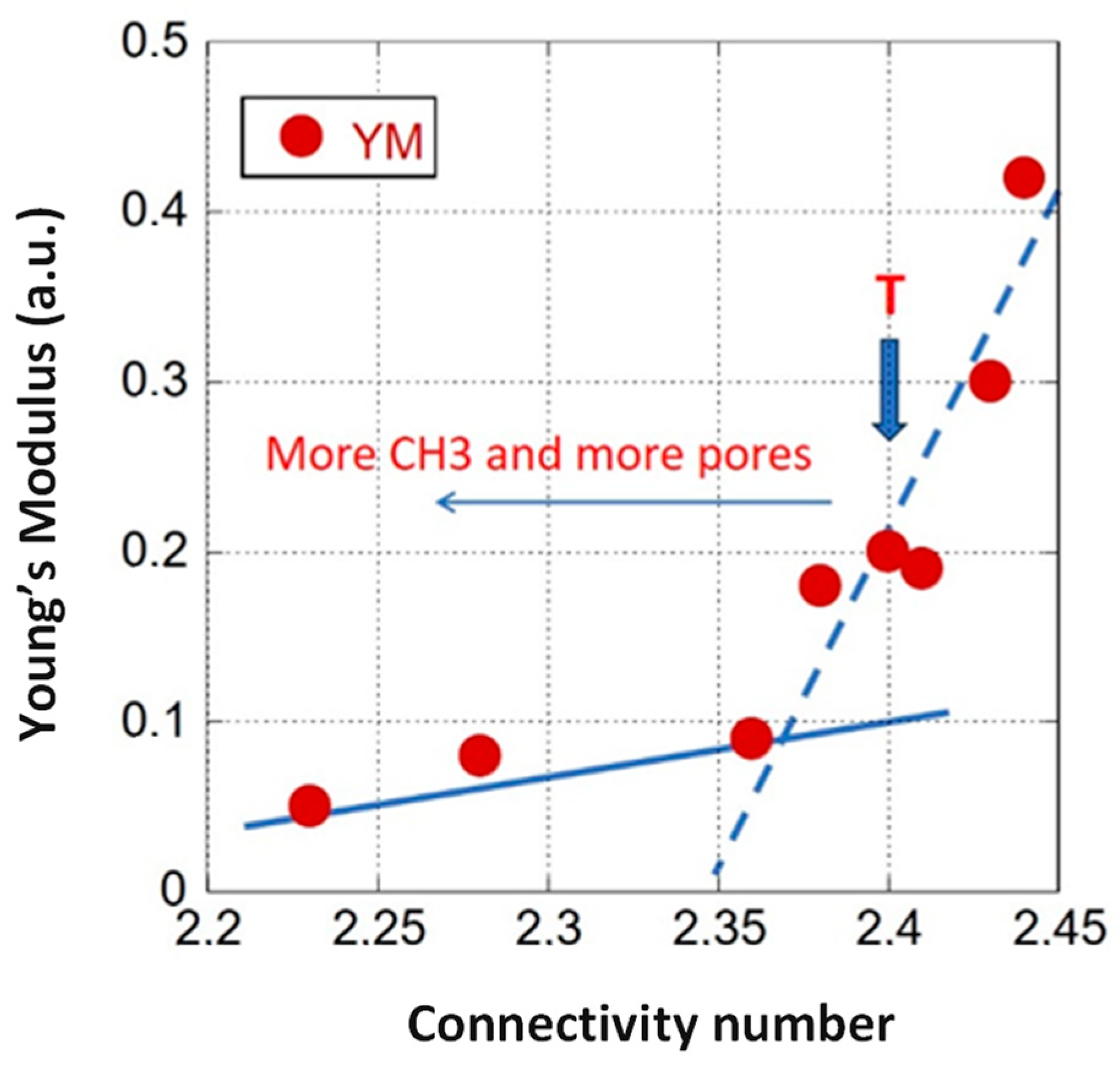
Two trends are evident: (1) mechanical strength increases sharply as the connectivity number approaches 2.35–2.4, marking the threshold for rigidity percolation, and (2) the introduction of terminal groups such as Si–CH3 reduces connectivity, lowering mechanical strength while also reducing the dielectric constant through the creation of pseudo-porosity.
The critical connectivity threshold corresponds to a value of 2.35–2.4 (Figure 16). The incorporation of CH3 groups induces a percolation-type transition, manifested as a sharp decrease in Young’s modulus (dotted line). It has been demonstrated that T-type materials (O3–Si–CH3) are located near the percolation threshold, depending on porosity, whereas materials containing D- or M-type groups remain below this threshold. Consequently, the Young’s modulus of “dense” OSG materials is significantly lower than that of dense SiO2 and is strongly influenced by both the type and concentration of organic terminal groups.
In current microelectronics applications, typical low-k dielectrics are primarily methyl-terminated (T-group) OSG materials, with a methyl concentration of approximately 15%–20%. These films generally exhibit Young’s modulus values in the range of 8–15 GPa (Table 4). Increasing the concentration of methyl groups or introducing D-type groups can enhance plasma resistance; however, this improvement comes at the expense of mechanical strength, as the additional organic substitution further reduces bond connectivity.

4.1.2. Mechanical Properties Versus Porosity (Porous OSG)

Advanced ULSI technology requires the implementation of ultralow-k dielectrics, which are primarily fabricated by introducing porosity. As previously mentioned, porous low-k films are typically prepared using the porogen approach, where porosity is controlled by varying the porogen loading. Subsequent porogen removal necessitates post-deposition treatments, such as ultraviolet (UV) light or electron beam-assisted annealing.
The matrix’s bond network is highly sensitive to specific irradiation conditions, making it difficult to directly compare low-k materials produced under different processing parameters—even when FTIR spectra indicate similar chemical compositions. Nevertheless, general trends have been reported, and comparisons of various studies suggest that mechanical properties evolve with porosity, following a percolation law with a percolation threshold between 35% and 45%.
The dependence of Young’s modulus on porosity is often described by empirical scaling laws or effective medium models. A widely used form is a power-law scaling according to Equation (4) [89]:
E(P) = E0 (1 − p)n,
  • E0—modulus of the dense matrix
  • p—volume fraction porosity (0–1)
  • n—exponent between ~2 and ~4 for silica-based films
Several theoretical approaches describe the modulus–porosity relationship:
(a)
Gibson–Ashby open-cell foam model (Equation (5)) [90]:
E/E0 ≈ (1 − p)2,
This theoretical model predicts the mechanical properties of materials containing open pores (open foams), typically with a length-to-diameter ratio greater than 5. By approximating the complex foam structure as a network of interconnected pores, it enables the estimation of key properties, such as the elastic modulus. Consequently, the model is most applicable to highly porous films where porosity exceeds the percolation threshold. At lower porosity levels—particularly near or below the percolation threshold—the n-value (a critical exponent in the model) is expected to be higher, reflecting the transition in mechanical behavior as the pore network becomes less continuous.
(b)
Hashin–Shtrikman bounds [91,92]
The Hashin-Shtrikman (HS) model is a micromechanical framework used to predict the effective elastic moduli of composite materials or heterogeneous systems, such as porous media or multiphase alloys. It establishes rigorous theoretical bounds (known as HS bounds) on these properties and, for certain idealized microstructures, provides exact analytical solutions. By accounting for phase interactions without requiring detailed microstructural information, the HS model bridges fundamental theoretical limits with practical material behavior.
(c)
Percolation-type behavior [93,94]
Near a critical porosity pc (usually ~0.6 for random pores), modulus follows Equation (6):
E ∝ (pcp)t,
with t ≈ 3–4. This captures the rapid fall-off near the mechanical percolation threshold. Several studies support the percolation-type scaling of elastic modulus with porosity, expressed as Equation (6). For instance, Rice [94] proposed a generalized model E/E0 = (1−p/pc), with the exponent n ranging between 0.5 and 4 depending on microstructural details. Kováčik [95] further demonstrated such behavior across various porous ceramics, fitting data to E=E0 (1−p/pc)f and finding f ≈ 1.1–1.7.
The experimental determination of Young’s modulus in thin films is typically conducted via nanoindentation, laser-induced surface acoustic waves, or ellipsometric porosimetry. Owing to their fundamentally different physical operating principles, these techniques may yield slightly divergent values, as each probes a different aspect of the film’s mechanical response. Although each method provides unique information, cross-evaluation can be performed using the results obtained from one technique.
Nanoindentation measurements of Young’s modulus for a comprehensive set of low-k films are plotted in Figure 17 as a function of porosity, the latter quantified by ellipsometric porosimetry. While a universal curve derived from the Gibson-Ashby Equation (5) provides a satisfactory formal fit to the entire dataset, a superior description is obtained by modeling the data with two separate curves. The left curve (1) characterizes the low-porosity regime, where mesopores remain discrete and unconnected. In this region, the reduction in Young’s modulus is attributed not to pore interconnection but to a decrease in the connectivity number of the solid matrix. In region 2, the connectivity remains relatively constant despite the introduction of some porosity. This is because the matrix can locally relax and redistribute stresses, allowing the network to accommodate small pores without significant loss of connectivity. Comprehensive theoretical details on the porosity dependence of stiffness are presented in the Supplementary Materials. Once porosity reaches a critical threshold in region 3, percolation pathways begin to form, and the connectivity rapidly decreases as the continuous pore network dominates the structural behavior. The percolation transition for mechanical properties (pc) is identified near 30% porosity, a threshold consistent with that reported for the dielectric breakdown field.
The percolation threshold (pc) is the critical fraction of occupied sites or bonds at which a connected path spans the entire system, forming an infinite connected cluster (the percolation cluster) [96]. Below pc all clusters are finite with probability 1; at and above pc an infinite cluster exists with probability 1 according to Equation (7):
P p = 0 , f o r p < p c > 0 , f o r p > p c ,
The value of pc depends on lattice geometry and the type of percolation problem. For example, in a triangular lattice, percolation occurs at ~30% site occupancy, whereas in a square lattice it requires >50% occupancy. In porous structures, the threshold can be even higher. Different formulations of the problem—site percolation, bond percolation, or continuum percolation—also influence the threshold value.
As already mentioned, generally Young’s modulus depends on many different factors related not only porosity but also their shape, type of ordering, etc. Several papers are related to these issues [35,97,98,99].
For instance, Yeap et al. [97] examined a series of OSG low-k films fabricated by both sol–gel and PECVD methods. A key finding was the determining role of pore topology in enabling the synthesis of dielectrics with an ultralow dielectric constant alongside a relatively high Young’s modulus. To elucidate the relationship between porosity, pore topology, and elastic modulus, a finite-element modeling approach was employed. This theoretical framework, when integrated with experimental nanoindentation (NI) data on elastic modulus, provided a powerful tool for predicting the pore morphology of diverse OSG films.
This pore structure prediction was validated using PALS. The porosity threshold for the transition from a closed-pore (non-overlapping) to an open-pore (overlapping) structure, as measured by PALS, was found to be consistent with the value derived from the finite-element model and nanoindentation analysis.
It was demonstrated that the dependence of the elastic moduli of PECVD-deposited OSG films on porosity is more accurately described by the randomly overlapping spherical solid model, whereas Sol–Gel OSG films fabricated via self-assembling (PMO) technology are better represented by a model corresponding to ordered, non-overlapping pores.
Li Han et al. [99] employed nanoindentation and the double cantilever beam technique to systematically examine the influence of porogen loading on the stiffness and cohesive fracture energy of a series of porous organosilicate glass (OSG) thin films. The films were synthesized via PECVD with controlled porosities between 7% and 45%.
The research resolved how porogen loading simultaneously alters the film’s network structure and porosity, and it delineated the distinct contributions of each factor to the mechanical properties. Experimental stiffness results were validated against micromechanical models and finite element simulations, confirming a high sensitivity to porosity. This correlation indicates that substantial improvements in mechanical integrity are achievable through strategic optimization of the pore architecture. A linear reduction in cohesive fracture energy with increasing porosity was also observed. This relationship supports a failure mechanism governed by fracture propagation along a planar path through the pore network.
Vanstreels et al. [35] evaluated effect of pore structure of porous low-k films on the measured elastic modulus mechanical properties of various low-k films with different porosity and pore size using various techniques such as nanoindentation, laser-induced surface acoustic wave spectroscopy (LAwave), and EP. The link between the elastic response of these nanoporous materials and their internal pore structure was investigated using positronium annihilation lifetime spectroscopy (PALS), EP, and diffusion experiments. For films with porosity above 25%, the broad band UV cured and narrow band UV cured films follow a similar linear trend and a clear transition is found near 25% of porosity. This transition correlates very well with the pores connectivity threshold (percolation threshold) that was observed by PALS technique and agrees well with the reported values of other nanoporous dielectric films in the literature. PALS measurements indicated that pores are interconnected (percolated) starting from 31% porosity. In addition to PALS, diffusion experiments were performed on nanoporous thin films using isopropanol as a probe molecule. From these measurements, diffusion coefficients were determined. The results showed that molecular diffusion of isopropanol occurred at porosity values well below the percolation threshold determined by PALS. This difference highlights that the percolation threshold depends on the diffusing species: stable molecules like isopropanol can traverse narrow necks connecting internal voids, whereas the PALS threshold reflects the interconnection of larger mesopores accessible to positronium.

4.2. Stiffness Enhancement Strategies in Low-k and Hybrid Glasses

Achieving high mechanical stiffness while maintaining low density and low dielectric permittivity is a central challenge in the design of low-k and hybrid glassy materials for microelectronics and nanotechnology applications. Various strategies have been explored, including molecular-level network design, hyperconnected precursors, organic cross-linking, and bond percolation control. Computational modeling, sol–gel synthesis, and plasma-enhanced deposition techniques have all contributed to understanding how network connectivity, precursor geometry, and non-affine deformations influence stiffness and other material properties. In the following, we review key studies that illustrate how these approaches enable the rational design of ultrastiff low-density glasses.
Figure 18 presents the fundamental building blocks of key dielectric materials used in interconnects. The classic SiO2 structure is shown in (a), with its tetrahedral coordination (Si bonded to four O atoms) and oxygen atoms bridging two silicon atoms. By replacing these bridging oxygen atoms with terminal methyl groups, a methyl-terminated low-k film is formed (b). This process reduces the material’s density and Young’s modulus, as the terminal groups decrease the network’s connectivity.
Han Li et al. [99] performed molecular dynamics simulations showing that organosilicates can be made substantially stiffer than amorphous silica while maintaining a lower mass density. This enhanced stiffness is achieved by incorporating organic cross-links that replace bridging oxygen atoms in the silica network (Figure 18c). The study explores how both organic cross-linking and terminal groups influence the stiffness and density of OSG materials. To this end, the authors used systematic modeling and analysis, examining structural properties (density, bond angles, and bond lengths) as well as mechanical properties (bulk modulus, shear modulus, and Young’s modulus) as functions of composition and network connectivity. The incorporation of organic bridging groups is expected to improve mechanical properties due to the higher bending rigidity of Si–CHₓ–Si bonds compared with Si–O–Si bonds. Another anticipated advantage is that OSG materials containing bridging organic groups can form films with ordered porosity, known as periodic mesoporous organosilicates (PMOs).
An even more aggressive strategy was proposed by Burg et al. [100], who demonstrated networks with silicon coordination numbers greater than four, achieving theoretical Young’s moduli of up to 48 GPa (Figure 18d). Using 1,3,5-silylbenzene precursors, they designed a hyperconnected network in which each silicon atom bonds to as many as five neighboring silicon atoms, exceeding the typical tetravalent coordination. This hyperconnectivity arises from a combination of Si–O–Si linkages and rigid benzene bridges, which raise the mean silicon network connectivity beyond the conventional limit of four (Figure 18a). To validate the computational model, a 1,3,5-benzene-based glass was synthesized via sol–gel chemistry from 1,3,5-(triethoxysilyl)benzene, yielding a film with a density of 1.52 g cm−3—significantly lower than fully dense silica (~2.2 g cm−3). Most silicon atoms adopt T-group configurations (three oxygen and one carbon neighbor), while 10.8% form Q-groups (four oxygen neighbors). Precursor dissociation produced a glass comprising ~2:1:1 molar ratios of 1,3,5-benzene, 1,3-benzene, and SiO2 structural units. Whereas optimized organosilica glasses deposited via PECVD typically achieve E≈16 GPa with ≤10 at.% carbon, the studied sol–gel glass contained 36 at.% carbon and exhibited E ≈ 23 ± 0.5 GPa at the same density. The high stiffness was attributed to rigid benzene bridges, which preserved network connectivity, whereas flexible precursors generated network terminations that lowered both connectivity and mechanical performance. Steric hindrance from bulky terminal groups (e.g., benzene) similarly reduced stiffness by disrupting network continuity.
King et al. [57] investigated the effect of network bond percolation on the properties of amorphous hydrogenated silicon carbide (a-SiC:H) thin films with both high and low dielectric constants. They examined how variations in the mean bond coordination number ⟨r⟩ influence mechanical, thermal, electrical, and optical properties, using constraint theory and bond percolation theory. The a-SiC:H films were deposited via PECVD, with deposition parameters adjusted to control hydrogen content and C/Si stoichiometry. This work provides experimental validation of constraint theory and bond percolation concepts for a-SiC:H, advancing the understanding of structure–property relationships in amorphous materials. These findings also inform the optimization of low-k materials for integrated circuits, where balancing low dielectric permittivity with high mechanical strength is essential. Based on their results, the authors proposed strategies such as incorporating stronger network bonds (e.g., Si–C instead of Si–O) or controlling weak van der Waals interactions to enhance structural integrity.

4.3. Non-Affine Deformations Control

The third research direction involved introducing hyperstiff precursor molecules with distinct geometrical characteristics to suppress nonaffine deformations. Kilic et al. [101,102,103] demonstrated that precursor design—specifically short bridging groups, molecular planarity, and symmetry—reduces nonaffine deformations and enhances stiffness. As a result, hyperconnected organosilicate networks formed from these precursors exhibit elastic properties superior to fully dense silica.
Molecular dynamics and constraint analyses identified the features that render precursors hyperstiff, offering the first quantitative evaluation of nonaffine deformations in hybrid organosilicate glasses. This represents a new framework to assess how both precursor geometry and network connectivity govern mechanical response.
Hybrid organic–inorganic glasses occupy a unique space between oxides and polymers, yet their inherently low density and brittleness limit mechanical robustness and hinder device integration. The proposed molecular design strategy simultaneously optimizes network connectivity and precursor geometry, enabling ultrastiff hybrid glasses that exceed the stiffness of dense silica while preserving low density.
Hyperconnectivity was achieved by increasing silicon connectivity beyond its coordination number of four, up to five through three oxygen bonds and two additional carbon bridges within the precursor [100,101]. This dual exploitation of hyperstiffness and hyperconnectivity constitutes a new design paradigm. Unlike traditional approaches that inevitably increase density by raising cross-link density, this method enhances stiffness via precursor geometry. The resulting networks open opportunities for the integration of robust, lightweight hybrid glasses into microelectronic, optical, and energy technologies.
Nevertheless, the presence of rigid fragments alone does not guarantee overall material rigidity. To maintain hydrophobicity, methyl terminals must constitute at least 12–15% of the material. Consequently, the rigid fragments are often embedded in a weakly rigid matrix at concentrations below the percolation threshold [104], limiting their ability to reinforce the network. Ensuring system-wide stiffness requires the formation of a percolating cluster of rigid fragments. Therefore, understanding the mechanisms of percolation cluster formation—including characteristics such as self-similarity and fractality near the percolation threshold—is essential. This knowledge enables the purposeful synthesis of elastic percolation clusters, providing a pathway to maximize rigidity in hybrid glasses.

5. Extended Summary of Experimental Trends

  • Experimental Trends
Experimentally, increasing porosity leads to distinct percolation-driven changes:
  • Leakage current rises sharply at relatively low porosity.
  • Breakdown voltage and mechanical modulus collapse abruptly at higher porosity, typically in the range of 20%–30% (depending on pore size and connectivity), just above the percolation threshold for open pores.
Thus, the percolation threshold for mechanical properties aligns more closely with that for dielectric breakdown, whereas leakage current reflects the earliest onset of connectivity, as it is shown in the schematic diagram in Figure 19.
2.
Distinct Percolation Classes
The percolation transition induces several classes of physical phenomena:
  • Transport phenomena: mass diffusion, electrical conduction, and leakage current.
  • Mechanical phenomena: degradation of stiffness and strength.
  • Nonlinear phenomena: dielectric breakdown.
At least three distinct percolation thresholds may therefore exist, each associated with a cluster of unique topology and backbone structure. The geometry of these clusters—and hence the thresholds—depends on the underlying physics of the phenomenon.
3.
Correlation Length and Timescales
The structure of a percolation cluster is characterized by the correlation length:
L c p p p c ν , p p c ,
where ν is the critical exponent of the correlation length. Dependent on dimensionality and structure. Percolation clusters include branched conductive paths and dead ends, which affect transport.
For mass transport, the relevant timescale is the diffusion time:
t L c = L c 2 D ,
where D is the diffusion coefficient and Lc is the correlation length of the conductivity cluster. The impulse relaxation time τp, which governs conductivity, is linked to diffusion via the Einstein relation:
q D = μ k T , μ = q τ p m ,
Thus, diffusion and conductivity can be described within a unified framework, characterized by equivalent timescales.
Leakage current is directly related to connectivity. As porosity, defects, or absorbed moisture approach the percolation threshold, leakage current can increase by several orders of magnitude, since isolated conductive regions merge into low-resistance pathways. This process is governed by the same correlation length Lc.
4.
Elastic and Breakdown Percolation
Mechanical stiffness is governed by a distinct elastic percolation cluster with correlation length L y c . This cluster exhibits a three-dimensional, foam-like architecture that differs from the quasi-1D conduction cluster.
For dielectric breakdown, an additional length scale arises:
α = q E L W , L E = W q E ,
where q is the elementary charge, E the electric field, and W a characteristic energy (e.g., W = kT). Breakdown occurs when the characteristic system length L becomes comparable to LE,. The relevant comparison is whether LE couples more strongly to Lc (conductivity cluster) or L y c (stiffness cluster).
Breakdown pathways are typically facilitated by structural defects (voids, cracks, impurities) or agglomerated conductive particles, which form branched, foam-like chains that act as preferential channels. These differ from conduction clusters, where zigzag quasi-1D paths hinder breakdown propagation. Because stiffness percolation clusters provide three-dimensional connectivity, breakdown pathways more closely coincide with stiffness pathways. This leads to the approximate equivalence:
L y c L p c γ p b ,
These theoretical considerations are consistent with experimental observations of dielectric breakdown in porous low-k materials. More detailed theoretical analysis and models can be found in “Supplement Materials” [105,106,107,108,109,110,111,112,113,114,115,116,117,118,119,120,121,122,123,124,125,126,127,128,129,130,131,132,133,134,135,136,137,138].

6. Conclusions

In this work, we reviewed percolation-related phenomena in porous low-k dielectrics and demonstrate their importance for mass transport, electrical conductivity, mechanical properties, and dielectric breakdown. A brief summary of the main processes is provided below.
  • Percolation Threshold for Leakage Current and mass transfer.
Leakage current is governed by charge carriers, typically electrons, hopping or tunneling through connected low-density regions comprising pores and damaged dielectric around pores. Current conduction requires only a minimal percolating path connecting the electrodes. This threshold is usually reached at relatively low porosity or damage levels, as a single percolating cluster is sufficient to sustain leakage. Organosilicate glass (OSG)-based low-k films prepared with a sacrificial porogen generally contain micropores, thought to arise from the substitution of bridging oxygen atoms in the silica network with sterically larger methyl groups (Figure 2). Additional microporosity may also be introduced during porogen removal. PALS measurements indicate that these micropores typically appear as closed [15,33], although they may still allow diffusion of stable molecules [33,34]. Consequently, they can form interconnected pathways for impurities such as adsorbed water, residual porogen species, or oxygen-deficient centers likely generated during UV curing. Exponential increases in leakage current via Poole–Frenkel (PF) emission along defect chains further accelerate reliability failures, as copper diffusion and moisture ingress propagate through connected pores, sharply reducing time-dependent dielectric breakdown (TDDB) lifetimes. These observations suggest that the percolation thresholds for leakage current and mass transport may substantially overlap.
2.
Percolation Threshold for Dielectric Breakdown
Dielectric breakdown differs fundamentally from leakage current. While leakage arises from the earliest formation of a conductive path, breakdown corresponds to the catastrophic failure of insulating capability across the device area. Breakdown involves:
  • local defect accumulation and hot-spot formation;
  • field enhancement at pore edges;
  • charge trapping;
  • progressive filament growth.
For breakdown to occur, multiple “near-percolating” paths across a wide area must interact. Thus, the effective percolation threshold for breakdown is higher than for leakage current: the material can tolerate more porosity before the breakdown field collapses. In other words, breakdown requires a dense network of connected pores and weak links, rather than a single tenuous path.
This statistical distinction explains why leakage current increases at a lower porosity threshold, whereas degradation of the breakdown voltage becomes significant only near the bulk-scale percolation limit [50,67]. Although many studies report that both leakage current and breakdown voltage increase with porosity, an illustrative example highlighting the distinction between the two was provided by [61]. In that study, films were fabricated using a tailored process developed by Urbanowicz [62] that effectively suppressed porogen residues and eliminated adsorbed water. As a result, the materials exhibited an unusual response: the leakage current showed no measurable dependence on porosity, whereas the breakdown field decreased roughly inversely with porosity. These findings support the interpretation that leakage current is predominantly governed by localized, impurity-assisted conduction pathways along pore walls, while dielectric breakdown is controlled by extended pore connectivity approaching the percolation threshold.
3.
Mechanical Percolation
Mechanical percolation in porous low-k dielectrics differs from electrical percolation. Properties such as elastic modulus, hardness, and fracture toughness degrade once pores coalesce into a connected network. Unlike leakage current, which requires only one conductive path, mechanical properties depend on the integrity of the global load-bearing skeleton. As a result, the threshold for mechanical failure is closer to that for dielectric breakdown than for leakage current, since both involve system-spanning connectivity of the pore network.
Even more complex behavior is observed in OSG low-k dielectrics. The characteristic double slope in the dependence of Young’s modulus on porosity can be explained by the presence of two distinct percolation thresholds (Figure 17). The first threshold occurs at low porosity and is associated with the replacement of bridging oxygen atoms by terminal methyl groups, which decreases the network connectivity in the OSG matrix [87,88]. This mechanism also accounts for the significantly reduced initial Young’s modulus values (E0) compared with dense SiO2 (15–20 GPa for dense OSG instead 70–80 for SiO2). The second slope corresponds to the percolation threshold related to porosity itself, which poses a major challenge for achieving mechanically robust ultra-low-k (ULK) materials.
To address the problem of the intrinsically low Young’s modulus at near-zero porosity (E0), several strategies have been proposed. The most common involve replacing bridging oxygen atoms with carbon-containing groups [99] or incorporating hyperconnected units such as benzene rings [100]. However, these modifications alone cannot ensure sufficient hydrophobicity, necessitating the additional introduction of terminal methyl groups. As a result, achieving a simultaneous improvement in both hydrophobicity and mechanical integrity remains a significant challenge in the development of OSG-based ultralow-k dielectrics. Importantly, the presence of multiple percolation thresholds underscores that both transport and mechanical properties in porous low-k materials are fundamentally controlled by network connectivity effects, providing a unifying framework for understanding their performance and guiding future material design.
Finally, a few remarks can be made regarding potential directions for future interconnect technologies. A clear trend toward reducing sensitivity to percolation-related challenges is the adoption of subtractive integration approaches, in which low-k materials are less exposed to aggressive plasma processing, thereby minimizing the likelihood of conductive path formation and dielectric constant degradation. Concurrently, the exploration of non-porous ultralow-k materials, such as the recently reported amorphous boron nitride [139] appears highly promising. Within the context of subtractive integration, the grafting of patterned metal surfaces onto low-k substrates also represents an interesting avenue, although further investigation of integration strategies is required [140,141]. Nevertheless, these approaches remain largely at the academic exploration stage, and more intensive studies on practical integration are critically needed.

Supplementary Materials

The following supporting information can be downloaded at: https://www.mdpi.com/article/10.3390/coatings15101138/s1. File S1.

Author Contributions

Conceptualization, M.R.B. and V.E.A.; methodology, V.E.A.; software, M.R., M.G.-O.; formal analysis, M.R., M.G.-O.; investigation, M.R.B.; resources, K.A.V.; data curation, M.G.-O.; writing—original draft preparation, M.R.B., V.E.A. and M.R.; writing—review and editing, M.R.B., M.G.-O.; visualization, M.G.-O.; supervision, M.R.B.; project administration, M.R.B.; funding acquisition, K.A.V. All authors have read and agreed to the published version of the manuscript.

Funding

This work was supported by the Russian Science Foundation [grant 23-79-30016] “The methodology of investigation and characterization of OSG low-k film properties” (G.M., K.A.V and M.R.B.) and grant 24-21-00356 “Development of Fundamentals for Controlling the Capture of Diffusing Particles by Traps Using External Fields: Numerical Simulation” (V.E.A).

Institutional Review Board Statement

The study does not require ethical approval.

Informed Consent Statement

Not applicable.

Data Availability Statement

The data presented in this study are available upon request from the corresponding authors.

Acknowledgments

The authors thank the Russian Science Foundation for financial support [grant No. 23-79-30016 (G.M., K.A.V., and M.R.B.) and grant No. 24-21-00356 (V.E.A.)]. We also thank A. Rezvanov for fruitful discussions at the early stage of this work.

Conflicts of Interest

The authors declare that they have no known competing financial interests or personal relationships that could have appeared to influence the work reported in this paper.

Abbreviations

The following abbreviations are used in this manuscript:
OSGOrganosilica glass
ULSIUltra large scale integrated
RCResistance-Capacitance
CTECoefficient of thermal expansion
NTRSNational Technology Roadmap for Semiconductors
ITRSInternational Technology Roadmap for Semiconductors
PECVDPlasma-enhanced chemical vapor deposition
ULKUltralow-k
IRDSInternational Roadmap of Devices and Systems
CMPChemical mechanical polishing
PALSPositron annihilation lifetime spectroscopy
EPEllipsometric porosimetry
VUVVacuum ultraviolet
TPOTop power only
BPOBottom power only
T&BPTop and bottom power
PFPoole-Frenkel
TDDBTime-dependent dielectric breakdown
ODCOxygen-deficient centers
FSGFluorinated silica
NRA-RBSNuclear reaction analysis- Rutherford backscattering
P-MSQMethylsilsequioxane
ALDAtomic layer deposition
FTIRFourier-transform infrared spectroscopy
HSHashin-Shtrikman
NINanoindentation

References

  1. Edelstein, D.; Heidenreich, J.; Goldblatt, R.; Cote, W.; Uzoh, C.; Lustig, N.; Roper, P.; McDevitt, T.; Motsiff, W.; Simon, A.; et al. Full copper wiring in a sub-0.25 μm CMOS ULSI technology. In Proceedings of the International Electron Devices Meeting (IEDM), Washington, DC, USA, 7–10 December 1997; pp. 773–776. [Google Scholar] [CrossRef]
  2. Andricacos, P.C.; Uzoh, C.; Dukovic, J.O.; Horkans, J.; Deligianni, H. Damascene copper electroplating for chip interconnections. IBM J. Res. Dev. 1998, 42, 567–574. [Google Scholar] [CrossRef]
  3. Havemann, R.H.; Hutchby, J.A. High-performance interconnects: An integration overview. Proc. IEEE 2001, 89, 586–601. [Google Scholar] [CrossRef]
  4. Ravindra, N.M. International Technology Roadmap for Semiconductors (ITRS). J. Electron. Mater. 2001, 30, 1478–1627. [Google Scholar]
  5. Ryan, E.T.; McKerrow, A.J.; Leu, J.; Ho, P.S. Materials issues and characterization of low-k dielectric materials. MRS Bull. 1997, 22, 49–54. [Google Scholar] [CrossRef]
  6. Harper, C. Electronic Packaging and Interconnection Handbook, 4th ed.; McGraw-Hill: New York, NY, USA, 2004. [Google Scholar]
  7. Ryan, E.T.; McKerrow, A.J.; Leu, J.; Ho, P.S. Materials issues and characterization of low-k dielectric materials. In Low Dielectric Constant Materials for IC Applications; Springer: Berlin/Heidelberg, Germany, 2003; pp. 23–74. [Google Scholar] [CrossRef]
  8. Hatton, B.D.; Landskron, K.; Hunks, W.J.; Bennett, M.R.; Shukaris, D.; Perovic, D.D.; Ozin, G.A. Materials chemistry for low-k materials. Mater. Today 2006, 9, 22–31. [Google Scholar] [CrossRef]
  9. Hong, N.; Zhang, Y.; Sun, Q.; Fan, W.; Li, M.; Xie, M.; Fu, W. The evolution of organosilicon precursors for low-k interlayer dielectric fabrication driven by integration challenges. Materials 2021, 14, 4827. [Google Scholar] [CrossRef]
  10. International Roadmap for Devices and Systems (IRDS). 2024 Update: More Moore; IEEE: Piscataway, NJ, USA, 2024; Available online: https://irds.ieee.org/images/files/pdf/2024/2024IRDS_MM.pdf (accessed on 25 August 2025).
  11. Baklanov, M.R.; Adelmann, C.; Zhao, L.; De Gendt, S. Advanced Interconnects: Materials, Processing, and Reliability. ECS J. Solid State Sci. Technol. 2015, 4, Y1–Y4. [Google Scholar] [CrossRef]
  12. Nakata, Y.; Ozaki, S.; Kudo, H. Multilevel interconnect technology for 45-nm node CMOS LSIs. Fujitsu Sci. Tech. J. 2010, 46, 120–127. [Google Scholar]
  13. Baklanov, M.R.; de Marneffe, J.F.; Shamiryan, D.; Urbanowicz, A.M.; Shi, H.; Rakhimova, T.V.; Huang, H.; Ho, P.S. Plasma processing of low-k dielectrics. J. Appl. Phys. 2013, 113, 041101. [Google Scholar] [CrossRef]
  14. Soulié, J.P.; Sankaran, K.; Van Troeye, B.; Leśniewska, A.; Pedreira, O.V.; Oprins, H.; Delie, G.; Fleischmann, C.; Boakes, L.; Rolin, C.; et al. Selecting Alternative Metals for Advanced Interconnects. J. Appl. Phys. 2024, 136, 171101. [Google Scholar] [CrossRef]
  15. Dull, T.L.; Frieze, W.E.; Gidley, D.W.; Sun, J.N.; Yee, A.F. Determination of pore size in mesoporous thin films from the annihilation lifetime of positronium. J. Phys. Chem. B 2001, 105, 4657–4662. [Google Scholar] [CrossRef]
  16. Baklanov, B.M.; Mogilnikov, K.P.; Polovinkin, V.G.; Dultsev, F.N. Determination of pore size distribution in thin films by el-lipsometric porosimetry. J. Vac. Sci. Technol. 2000, 18, 1385–1391. [Google Scholar] [CrossRef]
  17. Foran, B.J.; Kastenmeier, B.; Bright, D.S. Determination of pore-size distributions in low-k dielectric films by transmission electron microscopy. AIP Conf. Proc. 2003, 683, 556–561. [Google Scholar] [CrossRef]
  18. Sekhar, V.N. Mechanical characterization of black diamond (low-k) structures for 3D integrated circuit and packaging applications. In Nanoindentation in Materials Science; IntechOpen: London, UK, 2012. [Google Scholar] [CrossRef]
  19. Baklanov, M.; Ho, P.S.; Zschech, E. (Eds.) Advanced Interconnects for ULSI Technology; John Wiley & Sons: Hoboken, NJ, USA, 2012. [Google Scholar]
  20. Kresge, A.C.; Leonowicz, M.E.; Roth, W.J.; Vartuli, J.C.; Beck, J.S. Ordered mesoporous molecular sieves synthesized by a liquid-crystal template mechanism. Nature 1992, 359, 710–712. [Google Scholar] [CrossRef]
  21. Grill, A.; Perraud, L.; Patel, V.; Jahnes, C.; Cohen, S. Low dielectric constant SiCOH films as potential candidates for interconnect dielectrics. MRS Proc. 1999, 565, 107–116. [Google Scholar] [CrossRef]
  22. Grill, A. PECVD low and ultralow dielectric constant materials: From invention and research to products. J. Vac. Sci. Technol. B 2016, 34, 020801. [Google Scholar] [CrossRef]
  23. Iacopi, F.; Travaly, Y.; Eyckens, B.; Waldfried, C.; Abell, T.; Guyer, E.P.; Gage, D.M.; Dauskardt, R.H.; Sajavaara, T.; Houthoofd, K.; et al. Short-ranged structural rearrangement and enhancement of mechanical properties of organosilicate glasses induced by ultraviolet radiation. J. Appl. Phys. 2006, 99, 053511. [Google Scholar] [CrossRef]
  24. Baklanov, M.R.; Jousseaume, V.; Rakhimova, T.V.; Lopaev, D.V.; Mankelevich, Y.A.; Afanas’ev, V.V.; Shohet, J.L.; King, S.W.; Ryan, E.T. Impact of VUV photons on SiO2 and organosilicate low-k dielectrics: General behavior, practical applications, and atomic models. Appl. Phys. Rev. 2019, 6, 011301. [Google Scholar] [CrossRef]
  25. Chang, T.C.; Tsai, T.M.; Liu, P.T.; Chen, C.W.; Tseng, T.Y. Study on the effect of electron beam curing on low-k porous organosilicate glass (OSG) material. Thin Solid Films 2004, 469, 383–387. [Google Scholar] [CrossRef]
  26. Cho, S.M.; Papasouliotis, G.D.; Barnes, M. Method for Porogen Removal and Mechanical Strength Enhancement of Low-k Carbon Doped Silicon Oxide Using Low Thermal Budget Microwave Curing. U.S. Patent 7,892,985, 22 February 2011. [Google Scholar]
  27. Nguyen, P.T.; Fan, C.; Do, D.D.; Nicholson, D. On the cavitation-like pore blocking in ink-bottle pore: Evolution of hysteresis loop with neck size. J. Phys. Chem. C 2013, 117, 5475–5484. [Google Scholar] [CrossRef]
  28. Taylor, D.J.; Fleig, P.F.; Hietala, S.L. Technique for characterization of thin film porosity. Thin Solid Films 1998, 332, 257–261. [Google Scholar] [CrossRef]
  29. Furedi, M.; Manzano, C.V.; Marton, A.; Fodor, B.; Alvarez-Fernandez, A.; Guldin, S. Beyond the meso/macroporous boundary: Extending capillary condensation-based pore size characterization in thin films through tailored adsorptives. J. Phys. Chem. Lett. 2024, 15, 1420–1427. [Google Scholar] [CrossRef] [PubMed]
  30. Stassin, T.; Verbeke, R.; Cruz, A.J.; Rodríguez-Hermida, S.; Stassen, I.; Marreiros, J.; Krishtab, M.; Dickmann, M.; Egger, W.; Vankelecom, I.F.J.; et al. Porosimetry for thin films of metal–organic frameworks: A comparison of positron annihilation lifetime spectroscopy and adsorption-based methods. Adv. Mater. 2021, 33, 2006993. [Google Scholar] [CrossRef]
  31. Yim, J.H.; Seon, J.B.; Jeong, H.D.; Pu, L.S.; Baklanov, M.R.; Gidley, D.W. Morphological control of nanoporous films by the use of functionalized cyclodextrins as porogens. Adv. Funct. Mater. 2004, 14, 277–282. [Google Scholar] [CrossRef]
  32. Alvarez-Fernandez, A.; Reid, B.; Fornerod, M.J.; Taylor, A.; Divitini, G.; Guldin, S. Structural characterization of mesoporous thin film architectures: A tutorial overview. ACS Appl. Mater. Interfaces 2020, 12, 5195–5208. [Google Scholar] [CrossRef]
  33. Rasadujjaman, M.; Wang, Y.; Zhang, L.; Naumov, S.; Attallah, A.G.; Liedke, M.O.; Koehler, N.; Redzheb, M.; Vishnevskiy, A.S.; Seregin, D.S.; et al. A detailed ellipsometric porosimetry and positron annihilation spectroscopy study of porous organosilicate-glass films with various ratios of methyl terminal and ethylene bridging groups. Microporous Mesoporous Mater. 2020, 306, 110434. [Google Scholar] [CrossRef]
  34. Lépinay, M.; Djourelov, N.; Marinov, H.; Broussous, L.; Courouble, K.; Licitra, C.; Bertin, F.; Rouessac, V.; Ayral, A. Depth-resolved impact of integration process on porosity and solvent diffusion in a SiOCH low-k material. J. Porous Mater. 2014, 21, 475–484. [Google Scholar] [CrossRef]
  35. Vanstreels, K.; Wu, C.; Gonzalez, M.; Schneider, D.; Gidley, D.; Verdonck, P.; Baklanov, M.R. Effect of pore structure of nanometer scale porous films on the measured elastic modulus. Langmuir 2013, 29, 12025–12035. [Google Scholar] [CrossRef]
  36. Ben-Avraham, D. Diffusion and Reactions in Fractals and Disordered Systems; Cambridge University Press: Cambridge, UK, 2000. [Google Scholar]
  37. Liu, L.; Zheng, L.; Chen, Y. Macroscopic and microscopic anomalous diffusion in comb model with fractional dual-phase-lag model. Appl. Math. Model. 2018, 62, 629–637. [Google Scholar] [CrossRef]
  38. Goworek, T.; Ciesielski, K.; Jasińska, B.; Wawryszczuk, J. Positronium in large voids. Silicagel. Chem. Phys. Lett. 1997, 272, 91–95. [Google Scholar] [CrossRef]
  39. Kunnen, E.; Baklanov, M.R.; Franquet, A.; Shamiryan, D.; Rakhimova, T.V.; Urbanowicz, A.M.; Struyf, H.; Boullart, W. Effect of energetic ions on plasma damage of porous SiCOH low-k materials. J. Vac. Sci. Technol. B 2010, 28, 450–459. [Google Scholar] [CrossRef]
  40. Shamiryan, D.; Baklanov, M.R.; Vanhaelemeersch, S.; Maex, K. Comparative study of SiOCH low-k films with varied porosity interacting with etching and cleaning plasma. J. Vac. Sci. Technol. B 2002, 20, 1923–1928. [Google Scholar] [CrossRef]
  41. Shi, H.; Huang, H.; Bao, J.; Liu, J.; Ho, P.S.; Zhou, Y.; Pender, J.T.; Armacost, M.D.; Kyser, D. Role of ions, photons, and radicals in inducing plasma damage to ultra low-k dielectrics. J. Vac. Sci. Technol. B 2012, 30, 011206. [Google Scholar] [CrossRef]
  42. Uchida, S.; Takashima, S.; Hori, M.; Fukasawa, M.; Ohshima, K.; Nagahata, K.; Tatsumi, T. Plasma damage mechanisms for low-k porous SiOCH films due to radiation, radicals, and ions in the plasma etching process. J. Appl. Phys. 2008, 103, 073303. [Google Scholar] [CrossRef]
  43. Takeda, K.; Miyawaki, Y.; Takashima, S.; Fukasawa, M.; Oshima, K.; Nagahata, K.; Tatsumi, T.; Hori, M. Mechanism of plasma-induced damage to low-k SiOCH films during plasma ashing of organic resists. J. Appl. Phys. 2011, 109, 033303. [Google Scholar] [CrossRef]
  44. Rakhimova, T.V.; Rakhimov, A.T.; Mankelevich, Y.A.; Lopaev, D.V.; Kovalev, A.S.; Vasil’eva, A.N.; Zyryanov, S.M.; Kurchikov, K.; Proshina, O.V.; Voloshin, D.G.; et al. Low-k films modification under EUV and VUV radiation. J. Phys. D Appl. Phys. 2013, 47, 025102. [Google Scholar] [CrossRef]
  45. Nichols, M.T.; Sinha, H.; Wiltbank, C.A.; Antonelli, G.A.; Nishi, Y.; Shohet, J.L. Time-dependent dielectric breakdown of plasma-exposed porous organosilicate glass. Appl. Phys. Lett. 2012, 100, 112905. [Google Scholar] [CrossRef]
  46. Nichols, M.T.; Mavrakakis, K.; Lin, Q.; Shohet, J.L. The effects of plasma exposure and vacuum ultraviolet irradiation on photopatternable low-k dielectric materials. J. Appl. Phys. 2013, 114, 104107. [Google Scholar] [CrossRef]
  47. Ren, H.; Nichols, M.T.; Jiang, G.; Antonelli, G.A.; Nishi, Y.; Shohet, J.L. Defects in low-k organosilicate glass and their response to processing as measured with electron-spin resonance. Appl. Phys. Lett. 2011, 98, 102903. [Google Scholar] [CrossRef]
  48. Bittel, B.C.; Lenahan, P.M.; King, S.W. Ultraviolet radiation effects on paramagnetic defects in low-k dielectrics for ultralarge scale integrated circuit interconnects. Appl. Phys. Lett. 2010, 97, 063506. [Google Scholar] [CrossRef]
  49. Sinha, H.; Ren, H.; Nichols, M.T.; Lauer, J.L.; Tomoyasu, M.; Russell, N.M.; Jiang, G.; Antonelli, G.A.; Fuller, N.C.; Engelmann, S.U.; et al. The effects of vacuum ultraviolet radiation on low-k dielectric films. J. Appl. Phys. 2012, 112, 111101. [Google Scholar] [CrossRef]
  50. Ogawa, E.T.; Aubel, O. Electrical breakdown in advanced interconnect dielectrics. In Advanced Interconnects for ULSI Technology; Baklanov, M., Ho, P.S., Zschech, E., Eds.; John Wiley & Sons: Hoboken, NJ, USA, 2012; pp. 369–434. [Google Scholar] [CrossRef]
  51. Y Barbarin, Y.; Croes, K.; Roussel, P.J.; Li, Y.; Verdonck, P.; Baklanov, M.; Tokei, Z.; Zhao, L. Reliability characteristics of thin porous low-k silica-based interconnect dielectrics. In Proceedings of the 2013 IEEE International Reliability Physics Symposium (IRPS), Monterey, CA, USA, 14–18 April 2013; IEEE: Piscataway, NJ, USA, 2013; pp. 2F.3.1–2F.3.6. [Google Scholar] [CrossRef]
  52. Wu, C.; Li, Y.; Baklanov, M.R.; Croes, K. Electrical reliability challenges of advanced low-k dielectrics. ECS J. Solid State Sci. Technol. 2014, 4, N3065–N3070. [Google Scholar] [CrossRef]
  53. Suzumura, N.; Yamamoto, S.; Kodama, D.; Makabe, K.; Komori, J.; Murakami, E.; Maegawa, S.; Kubota, K. A new TDDB degradation model based on Cu ion drift in Cu interconnect dielectrics. In Proceedings of the 2006 IEEE International Reliability Physics Symposium, San Jose, CA, USA, 26–30 March 2006; IEEE: Piscataway, NJ, USA, 2006; pp. 484–489. [Google Scholar] [CrossRef]
  54. Tokei, Z.; Sutcliffe, V.; Demuynck, S.; Iacopi, F.; Roussel, P.; Beyer, G.P.; Hoofman, R.J.O.M.; Maex, K. Impact of the barrier/dielectric interface quality on reliability of Cu porous-low-k interconnects. In Proceedings of the 2004 IEEE International Reliability Physics Symposium, Phoenix, AZ, USA, 25–29 April 2004; IEEE: Piscataway, NJ, USA, 2004; pp. 326–332. [Google Scholar] [CrossRef]
  55. Baklanov, M.R.; Gismatulin, A.A.; Naumov, S.; Perevalov, T.V.; Gritsenko, V.A.; Vishnevskiy, A.S.; Rakhimova, T.V.; Vorotilov, K.A. Comprehensive Review on the Impact of Chemical Composition, Plasma Treatment, and Vacuum Ultraviolet (VUV) Irradiation on the Electrical Properties of Organosilicate Films. Polymers 2024, 16, 2230. [Google Scholar] [CrossRef]
  56. Agmon, N. The Grotthuss mechanism. Chem. Phys. Lett. 1995, 244, 456–462. [Google Scholar] [CrossRef]
  57. King, S.W.; Bielefeld, J.; Xu, G.; Lanford, W.A.; Matsuda, Y.; Dauskardt, R.H.; Kim, N.; Hondongwa, D.; Olasov, L.; Daly, B.; et al. Influence of network bond percolation on the thermal, mechanical, electrical and optical properties of high and low-k a-SiC:H thin films. J. Non-Cryst. Solids 2013, 379, 67–79. [Google Scholar] [CrossRef]
  58. Gerelt-Od, M.; Kolesnikova, T.G.; Mokrushev, P.A.; Vishnevskiy, A.S.; Vorotilov, K.A.; Gismatulin, A.A.; Gritsenko, V.A.; Baklanov, M.R. Exploring the relationship between electrical characteristics and changes in chemical composition and structure of OSG low-k films under thermal annealing. Coatings 2024, 14, 1412. [Google Scholar] [CrossRef]
  59. Zheng, H.; Guo, X.; Pei, D.; Ryan, E.T.; Nishi, Y.; Shohet, J.L. Effects of vacuum ultraviolet irradiation on trapped charges and leakage currents of low-k organosilicate dielectrics. Appl. Phys. Lett. 2015, 106, 192902. [Google Scholar] [CrossRef]
  60. Ren, H.; Jiang, G.; Antonelli, G.A.; Nishi, Y.; Shohet, J.L. The nature of the defects generated from plasma exposure in pristine and ultraviolet-cured low-k organosilicate glass. Appl. Phys. Lett. 2011, 98, 251906. [Google Scholar] [CrossRef]
  61. Vanstreels, K.; Ciofi, I.; Barbarin, Y.; Baklanov, M.R. Influence of porosity on dielectric breakdown of ultralow-k dielectrics. J. Vac. Sci. Technol. B 2013, 31, 051202. [Google Scholar] [CrossRef]
  62. Urbanowicz, A.M.; Vanstreels, K.; Verdonck, P.; Shamiryan, D.; De Gendt, S.; Baklanov, M.R. Improving mechanical robustness of ultralow-k SiOCH plasma enhanced chemical vapor deposition glasses by controlled porogen decomposition prior to UV-hardening. J. Appl. Phys. 2010, 107, 104104. [Google Scholar] [CrossRef]
  63. Ogawa, E.T.; Kim, J.; Haase, G.S.; Mogul, H.C.; McPherson, J.W. Leakage, breakdown, and TDDB characteristics of porous low-k silica-based interconnect dielectrics. In Proceedings of the 2003 IEEE International Reliability Physics Symposium Proceedings, 41st Annual, Dallas, TX, USA, 30 March–4 April 2003; IEEE: Piscataway, NJ, USA, 2003; pp. 166–172. [Google Scholar] [CrossRef]
  64. Lee, S.C.; Oates, A.S. Reliability limitations to the scaling of porous low-k dielectrics. In Proceedings of the 2011 International Reliability Physics Symposium, Monterey, CA, USA, 10–14 April 2011; IEEE: Piscataway, NJ, USA, 2011; pp. 2F.5.1–2F.5.5. [Google Scholar] [CrossRef]
  65. Li, Y.; Ciofi, I.; Carbonell, L.; Heylen, N.; Van Aelst, J.; Baklanov, M.R.; Groeseneken, G.; Maex, K.; Tőkei, Z. Influence of absorbed water components on SiOCH low-k reliability. J. Appl. Phys. 2008, 104, 034104. [Google Scholar] [CrossRef]
  66. Jinnai, B.; Nozawa, T.; Samukawa, S. Damage mechanism in low-dielectric (low-k) films during plasma processes. J. Vac. Sci. Technol. B 2008, 26, 1926–1932. [Google Scholar] [CrossRef]
  67. Van Besien, E.; Pantouvaki, M.; Zhao, L.; De Roest, D.; Baklanov, M.R.; Tőkei, Z.; Beyer, G. Influence of porosity on electrical properties of low-k dielectrics. Microelectron. Eng. 2012, 92, 59–61. [Google Scholar] [CrossRef]
  68. Hong, C.; Milor, L. Effect of porosity on charge transport in porous ultra-low-k dielectrics. In Proceedings of the 2006 International Interconnect Technology Conference, Burlingame, CA, USA, 5–7 June 2006; IEEE: Piscataway, NJ, USA, 2006; pp. 140–142. [Google Scholar] [CrossRef]
  69. Lloyd, J.R.; Murray, C.E.; Ponoth, S.; Cohen, S.; Liniger, E. The effect of Cu diffusion on the TDDB behavior in low-k interlevel dielectrics. Microelectron. Reliab. 2006, 46, 1643–1647. [Google Scholar] [CrossRef]
  70. Michelon, J.; Hoofman, R.J. Moisture influence on porous low-k reliability. IEEE Trans. Device Mater. Reliab. 2006, 6, 169–174. [Google Scholar] [CrossRef]
  71. Lee, S.C.; Oates, A.S.; Chang, K.M. Fundamental understanding of porous low-k dielectric breakdown. In Proceedings of the 2009 IEEE International Reliability Physics Symposium, Montreal, QC, Canada, 26–30 April 2009; IEEE: Piscataway, NJ, USA, 2009; pp. 481–485. [Google Scholar] [CrossRef]
  72. Miyazaki, H.; Kodama, D.; Suzumura, N. The observation of stress-induced leakage current of damascene interconnects after bias temperature aging. In Proceedings of the 2008 IEEE International Reliability Physics Symposium, Phoenix, AZ, USA, 27 April–1 May 2008; IEEE: Piscataway, NJ, USA, 2008; pp. 150–157. [Google Scholar] [CrossRef]
  73. Wu, C.; Li, Y.; Barbarin, Y.; Ciofi, I.; Croes, K.; Bömmels, J.; De Wolf, I.; Tőkei, Z. Correlation between field dependent electrical conduction and dielectric breakdown in a SiCOH based low-k (k = 2.0) dielectric. Appl. Phys. Lett. 2013, 103, 032902. [Google Scholar] [CrossRef]
  74. Wu, E.Y.; Vollertsen, R.P. On the Weibull shape factor of intrinsic breakdown of dielectric films and its accurate experimental determination. Part I: Theory, methodology, experimental techniques. IEEE Trans. Electron Devices 2003, 49, 2131–2140. [Google Scholar] [CrossRef]
  75. Ogawa, E.T.; McPherson, J.W.; Rosal, J.A.; Dickerson, K.J.; Chiu, T.C.; Tsung, L.Y.; Jain, M.K.; Bonifield, T.D.; Ondrusek, J.C.; McKee, W.R. Stress-induced voiding under vias connected to wide Cu metal leads. In Proceedings of the 2002 IEEE International Reliability Physics Symposium, Dallas, TX, USA, 7–11 April 2002; Proceedings, 40th Annual (Cat. No. 02CH37320). IEEE: Piscataway, NJ, USA, 2002; pp. 312–321. [Google Scholar] [CrossRef]
  76. Hong, C.; Milor, L. Electric field enhancement caused by porosity in ultra-low-k dielectrics. In Proceedings of the ISSM 2005, IEEE International Symposium on Semiconductor Manufacturing, San Jose, CA, USA, 13–15 September 2005; IEEE: Piscataway, NJ, USA, 2005; pp. 434–437. [Google Scholar] [CrossRef]
  77. Orlov, A.A.; Rezvanov, A.A.; Gvozdev, V.A.; Orlov, G.A.; Seregin, D.S.; Kuznetsov, P.I.; Blumberg, T.; Veselov, A.A.; Suzuki, T.; Morozov, E.N.; et al. Dielectric barrier in the subtractive process of formation of a copper metallization system. Russ. Microelectron. 2022, 51, 470–479. [Google Scholar] [CrossRef]
  78. Chen, F.; Li, B.; Lee, T.; Christiansen, C.; Gill, J.; Angyal, M.; Shinosky, M.; Burke, C.; Hasting, W.; Austin, R.; et al. Technology reliability qualification of a 65nm CMOS Cu/low-k BEOL interconnect. In Proceedings of the 2006 13th International Symposium on the Physical and Failure Analysis of Integrated Circuits, Singapore, 3–7 July 2006; IEEE: Piscataway, NJ, USA, 2006; pp. 97–105. [Google Scholar] [CrossRef]
  79. Paquette, M.M.; Nordell, B.J.; Caruso, A.N.; Sato, M.; Fujiwara, H.; King, S.W. Optimization of amorphous semiconductors and low-/high-k dielectrics through percolation and topological constraint theory. MRS Bull. 2017, 42, 39–44. [Google Scholar] [CrossRef]
  80. Armini, S.; Prado, J.L.; Krishtab, M.; Swerts, J.; Verdonck, P.; Meersschaut, J.; Conard, T.; Blauw, M.; Struyf, H.; Baklanov, M.R. Pore sealing of k 2.0 dielectrics assisted by self-assembled monolayers deposited from vapor phase. Microelectron. Eng. 2014, 120, 240–245. [Google Scholar] [CrossRef]
  81. Zhao, L.; Tokei, Z.; Gischia, G.G.; Pantouvaki, M.; Croes, K.; Beyer, G. A novel test structure to study intrinsic reliability of barrier/low-k. In Proceedings of the 2009 IEEE International Reliability Physics Symposium, Montreal, QC, Canada, 26–30 April 2009; IEEE: Piscataway, NJ, USA, 2009; pp. 848–850. [Google Scholar] [CrossRef]
  82. Frot, T.; Volksen, W.; Purushothaman, S.; Bruce, R.; Dubois, G. Application of the Protection/Deprotection Strategy to the Science of Porous Materials. Adv. Mater. 2011, 23, 2828–2832. [Google Scholar] [CrossRef]
  83. Frot, T.; Volksen, W.; Purushothaman, S.; Bruce, R.L.; Magbitang, T.; Miller, D.C.; Sherwood, M.H.; Dubois, G. Post Porosity Plasma Protection: Scaling of Efficiency with Porosity. Adv. Funct. Mater. 2012, 22, 3043–3050. [Google Scholar] [CrossRef]
  84. Zhang, L.; Ljazouli, R.; Lefaucheux, P.; Tillocher, T.; Dussart, R.; Mankelevich, Y.A.; de Marneffe, J.-F.; de Gendt, S.; Baklanov, M.R. Low damage cryogenic etching of porous organosilicate low-k materials using SF6/O2/SiF4. ECS J. Solid State Sci. Technol. 2013, 2, N131–N139. [Google Scholar] [CrossRef]
  85. Vanstreels, K.; Li, H.; Vlassak, J.J. Mechanical reliability of low-k dielectrics. In Advanced Interconnects for ULSI Technology, 1st ed.; Baklanov, M.R., Ho, P., Zschech, E., Eds.; Springer: New York, NY, USA, 2012; Volume 10, pp. 339–367. [Google Scholar] [CrossRef]
  86. Phillips, J.C.; Thorpe, M.F. Constraint Theory, Vector Percolation and Glass Formation. Solid State Commun. 1985, 53, 699–702. [Google Scholar] [CrossRef]
  87. Burkey, D.D.; Gleason, K.K. Structure and mechanical properties of thin films deposited from 1,3,5-trimethyl-1,3,5-trivinylcyclotrisiloxane and water. J. Appl. Phys. 2003, 93, 5143–5150. [Google Scholar] [CrossRef]
  88. Ross, D. Chemical Vapor Deposition of Organosilicon Composite Thin Films for Porous Low-k Films. Ph.D. Thesis, MIT, Cambridge, MA, USA, 2005. [Google Scholar]
  89. Plawsky, J.L.; Achanta, R.; Cho, W.; Rodriguez, O.; Saxena, R.; Gill, W.N. Mechanical and transport properties of low-k dielectrics. In Dielectric Films for Advanced Microelectronics; Baklanov, M.R., Green, M., Maex, K., Eds.; John Wiley & Sons: New York, NY, USA, 2007; pp. 137–197. [Google Scholar] [CrossRef]
  90. Ashby, M.F.; Gibson, L.J. Cellular Solids: Structure and Properties; Press Syndicate of the University of Cambridge: Cambridge, UK, 1997; pp. 175–231. [Google Scholar]
  91. Hashin, Z.; Shtrikman, S. A variational approach to the theory of the elastic behaviour of multiphase materials. J. Mech. Phys. Solids 1963, 11, 127–140. [Google Scholar] [CrossRef]
  92. Sa, Y.K.; Bang, J.; Son, J.; Yu, D.Y.; Kim, Y.C. Enhanced thermo–mechanical reliability of ultralow-k dielectrics with self-organized molecular pores. Materials 2021, 14, 2284. [Google Scholar] [CrossRef]
  93. Farago, O.; Kantor, Y. Entropic elasticity of phantom percolation networks. Europhys. Lett. 2000, 52, 413–419. [Google Scholar] [CrossRef]
  94. Rice, R.W. Use of normalized porosity in models for the porosity dependence of mechanical properties. J. Mater. Sci. 2005, 40, 983–989. [Google Scholar] [CrossRef]
  95. Kováčik, J. Correlation between Young’s modulus and porosity in porous materials. J. Mater. Sci. Lett. 1999, 18, 1007–1010. [Google Scholar] [CrossRef]
  96. Stauffer, D.; Aharony, A. Introduction to Percolation Theory; Taylor & Francis: London, UK, 2018. [Google Scholar]
  97. Yeap, K.B.; Kopycinska-Mueller, M.; Chen, L.; Chen, Y.; Jungmann, M.; Krause-Rehberg, R.; Mahajan, S.; Vlassak, J.; Gall, M.; Zschech, E. The effect of the pore topology on the elastic modulus of organosilicate glasses. J. Mater. Res. 2013, 28, 1262–1268. [Google Scholar] [CrossRef]
  98. Michalak, D.J.; Blackwell, J.M.; Torres, J.M.; Gleason, K.K.; Grill, A.; Le, Q.T.; Gates, S.M.; Neumayer, D.A.; Noori, A.M.; Smith, B.C.; et al. Porosity Scaling Strategies for Low-k Films. J. Mater. Res. 2015, 30, 3363–3385. [Google Scholar] [CrossRef]
  99. Li, H.; Lin, Y.; Tsui, T.Y.; Vlassak, J.J. The effect of porogen loading on the stiffness and fracture energy of brittle organosilicates. J. Mater. Res. 2009, 24, 107–116. [Google Scholar] [CrossRef]
  100. Burg, J.A.; Oliver, M.S.; Frot, T.J.; Sherwood, M.; Lee, V.; Dubois, G.; Dauskardt, R.H. Hyperconnected molecular glass network architectures with exceptional elastic properties. Nat. Commun. 2017, 8, 1019. [Google Scholar] [CrossRef]
  101. Kilic, K.I.; Dauskardt, R.H. Design of Ultrastiff Organosilicate Hybrid Glasses. Adv. Funct. Mater. 2019, 29, 1904890. [Google Scholar] [CrossRef]
  102. Kilic, K.I.; Dauskardt, R.H. Mechanically Reliable Hybrid Organosilicate Glasses for Advanced Interconnects. J. Vac. Sci. Technol. B 2020, 38, 060601. [Google Scholar] [CrossRef]
  103. De Keer, L.; Kilic, K.I.; Van Steenberge, P.H.; Daelemans, L.; Kodura, D.; Frisch, H.; De Clerck, K.; Reyniers, M.-F.; Barner-Kowollik, C.; Dauskardt, R.H.; et al. Computational Prediction of the Molecular Configuration of Three-Dimensional Network Polymers. Nat. Mater. 2021, 20, 1422–1430. [Google Scholar] [CrossRef]
  104. Rasadujjaman, M.; Wang, X.; Wang, Y.; Zhang, J.; Arkhincheev, V.E.; Baklanov, M.R. Analytical study of porous organosilicate glass films prepared from mixtures of 1,3,5- and 1,3-alkoxysilylbenzenes. Materials 2021, 14, 1881. [Google Scholar] [CrossRef]
  105. Broadbent, S.R.; Hammersley, J.M. Percolation processes: I. Crystals and mazes. Math. Proc. Camb. Philos. Soc. 1957, 53, 629–641. [Google Scholar] [CrossRef]
  106. Kesten, H. The critical probability of bond percolation on the square lattice equals 1/21/21/2. Commun. Math. Phys. 1980, 74, 41–59. [Google Scholar] [CrossRef]
  107. Aizenman, M.; Barsky, D.J. Sharpness of the Phase Transition in Percolation Models. Commun. Math. Phys. 1987, 108, 489–526. [Google Scholar] [CrossRef]
  108. Grimmett, G.R. Inequalities and entanglements for percolation and random-cluster models. In Perplexing Problems in Probability: Festschrift in Honor of Harry Kesten; Birkhäuser: Boston, MA, USA, 1999; pp. 91–105. [Google Scholar] [CrossRef]
  109. Grassberger, P. On the Critical Behavior of the General Epidemic Process and Dynamical Percolation. Math. Biosci. 1983, 63, 157–172. [Google Scholar] [CrossRef]
  110. Cohen, R.; Havlin, S. Complex Networks: Structure, Robustness and Function; Cambridge University Press: Cambridge, UK, 2010. [Google Scholar]
  111. Sahimi, M. Flow and Transport in Porous Media and Fractured Rock: From Classical Methods to Modern Approaches; John Wiley & Sons: Hoboken, NJ, USA, 2011. [Google Scholar]
  112. Newman, M.E.J. Spread of epidemic disease on networks. Phys. Rev. E 2002, 66, 016128. [Google Scholar] [CrossRef]
  113. Beggs, J.M.; Plenz, D. Neuronal avalanches in neocortical circuits. J. Neurosci. 2003, 23, 11167–11177. [Google Scholar] [CrossRef]
  114. Gupta, P.; Kumar, P.R. The capacity of wireless networks. IEEE Trans. Inf. Theory 2000, 46, 388–404. [Google Scholar] [CrossRef]
  115. Achlioptas, D.; D’Souza, R.M.; Spencer, J. Explosive percolation in random networks. Science 2009, 323, 1453–1455. [Google Scholar] [CrossRef] [PubMed]
  116. De Gennes, P.G. Scaling Concepts in Polymer Physics; Cornell University Press: Ithaca, NY, USA, 1979. [Google Scholar]
  117. Ashby, M.F.; Medalist, R.M. The Mechanical Properties of Cellular Solids; Pergamon Press: Oxford, UK, 1983. [Google Scholar] [CrossRef]
  118. Gibson, I.J.; Ashby, M.F. The Mechanics of Three-Dimensional Cellular Materials. Proc. R. Soc. Lond. A 1982, 382, 43–59. [Google Scholar] [CrossRef]
  119. Gibson, L.J.; Ashby, M.F.; Schajer, G.S.; Robertson, C.I. The Mechanics of Two-Dimensional Cellular Materials. Proc. R. Soc. Lond. A 1982, 382, 25–42. [Google Scholar] [CrossRef]
  120. Deshpande, V.S.; Ashby, M.F.; Fleck, N.A. Foam Topology: Bending versus Stretching Dominated Architectures. Acta Mater. 2001, 49, 1035–1040. [Google Scholar] [CrossRef]
  121. Efros, A.L.; Shklovskii, B.I. Critical Behaviour of Conductivity and Dielectric Constant Near the Metal-Non-Metal Transition Threshold. Phys. Status Solidi B 1976, 76, 475–485. [Google Scholar] [CrossRef]
  122. Clerc, J.P.; Giraud, G.; Laugier, J.M.; Luck, J.M. The Electrical Conductivity of Binary Disordered Systems, Percolation Clusters, Fractals and Related Models. Adv. Phys. 1990, 39, 191–309. [Google Scholar] [CrossRef]
  123. Bergman, D.J.; Stroud, D. Physical Properties of Macroscopically Inhomogeneous Media. In Solid State Physics; Academic Press: San Diego, CA, USA, 1992; Volume 46, pp. 147–269. [Google Scholar] [CrossRef]
  124. Kumar, A.; Vidhyadhiraja, N.S.; Kulkarni, G.U. Current distribution in conducting nanowire networks. J. Appl. Phys. 2017, 122, 045101. [Google Scholar] [CrossRef]
  125. Mandelbrot, B.B. Fractals: Form, Chance, and Dimension; W. H. Freeman and Company: New York, NY, USA, 2020. [Google Scholar]
  126. Richardson, L.F. The Problem of Contiguity: An Appendix to Statistics of Deadly Quarrels. Gen. Syst. Yearb. 1961, 6, 139–187. [Google Scholar]
  127. Addison, P.S. Fractals and Chaos: An Illustrated Course; CRC Press: Boca Raton, FL, USA, 1997. [Google Scholar]
  128. Weiss, G.H.; Havlin, S. Some properties of a random walk on a comb structure. Phys. A 1986, 134, 474–482. [Google Scholar] [CrossRef]
  129. Havlin, S.; Kiefer, J.E.; Weiss, G.H. Anomalous diffusion on a random comblike structure. Phys. Rev. A 1987, 36, 1403. [Google Scholar] [CrossRef]
  130. Murthy, K.P.N.; Kehr, K.W. Mean first-passage time of random walks on a random lattice. Phys. Rev. A 1989, 40, 2082. [Google Scholar] [CrossRef]
  131. Dhar, D. Diffusion and drift on percolation networks in an external field. J. Phys. A Math. Gen. 1984, 17, L257–L262. [Google Scholar] [CrossRef]
  132. Tateishi, A.A.; Ribeiro, H.V.; Sandev, T.; Petreska, I.; Lenzi, E.K. Quenched and annealed disorder mechanisms in comb models with fractional operators. Phys. Rev. E 2020, 101, 022135. [Google Scholar] [CrossRef]
  133. Lubashevskii, I.A.; Zemlyanov, A.A. Continuum description of anomalous diffusion on a comb structure. J. Exp. Theor. Phys. 1998, 87, 700–713. [Google Scholar] [CrossRef]
  134. Alexander, S.; Orbach, R. Density of states on fractals: “fractons”. J. Phys. Lett. 1982, 43, 625–631. [Google Scholar] [CrossRef]
  135. Gefen, Y.; Aharony, A.; Mandelbrot, B.B.; Kirkpatrick, S. Solvable fractal family, and its possible relation to the backbone at percolation. Phys. Rev. Lett. 1981, 47, 1771. [Google Scholar] [CrossRef]
  136. Chamon, C. Quantum glassiness in strongly correlated clean systems: An example of topological overprotection. Phys. Rev. Lett. 2005, 94, 040402. [Google Scholar] [CrossRef] [PubMed]
  137. Haah, J. Local stabilizer codes in three dimensions without string logical operators. Phys. Rev. A 2011, 83, 042330. [Google Scholar] [CrossRef]
  138. Nandkishore, R.M.; Hermele, M. Fractons. Annu. Rev. Condens. Matter Phys. 2019, 10, 295–313. [Google Scholar] [CrossRef]
  139. Hong, S.; Lee, C.S.; Lee, M.H.; Lee, Y.; Ma, K.Y.; Kim, G.; Yoon, S.I.; Ihm, K.; Kim, K.-J.; Shin, T.J.; et al. Ultralow-dielectric-constant amorphous boron nitride. Nature 2020, 582, 511–514. [Google Scholar] [CrossRef] [PubMed]
  140. Cao, L.; Guo, X.; Li, M. Research on the properties of low-k films grafted on Cu (111) surface via electrochemical reduction of aryl diazonium salts. Appl. Surf. Sci. 2025, 684, 161959. [Google Scholar] [CrossRef]
  141. Multia, J.; Kravchenko, D.E.; Rubio-Gimenez, V.; Philip, A.; Ameloot, R.; Karppinen, M. Nanoporous Metal–Organic Framework Thin Films Prepared Directly from Gaseous Precursors by Atomic and Molecular Layer Deposition: Implications for Microelectronics. ACS Appl. Nano Mater. 2023, 6, 827–831. [Google Scholar] [CrossRef]
Figure 1. Predictions by NTRS 1997 (solid lines), ITRS 2008 and IRDS 2024. The delay and corrections of dielectric constant are related to difficulty of integration of porous dielectric materials. It is presently expected that the materials with k = 2.8–3.2 (p < 10%) will be used until 2029 (Ref. [10], Table MM13, page 15). The left graph (1998–2012) redrawn from the data presented in the paper [11]. Materials with k = 2.2–2.55 might be needed starting from 2030. It is important that industry has not been able to integrate so far low-k materials with porosity exceeding the percolation threshold.
Coatings 15 01138 g001
Figure 2. Schematic illustration depicting various types of porosity in low-k films and their respective adsorption isotherms.
Coatings 15 01138 g002
Figure 3. Profile of oxygen (O), carbon (C) and fluorine (F) concentrations after exposure of 19% (top graphs) and 40% (bottom graphs) porous low-k films in oxygen and fluorine based plasmas. Thin curves represent films before plasma treatment, bold dashed curves—after plasma treatment [40]. Reproduced from J. Vac. Sci. Technol. B 20, 1923–1928 (2002) [40] with permission from the American Vacuum Society (AVS).
Coatings 15 01138 g003
Figure 4. Change in FTIR absorbance at 1275 cm−1 associated with the Si-CH3 after exposure in TPO, BPO, and T&BP conditions during the time necessary to remove certain amount of resist. In the case of TPO the absorbance completely disappears, while for BPO and T&BP the absorbance partially remains.
Coatings 15 01138 g004
Figure 5. Quantum yield of VUV induced damage versus porosity. Redrawn using data from Ref. [44]. ©IOP Publishing. Reproduced with permission. All rights reserved.
Coatings 15 01138 g005
Figure 6. Schematic illustration of percolation in porous materials. The diagram depicts the topological transition responsible for the sharp increase in leakage current observed near the percolation threshold. (a) Isolated pores at porosity p below the critical porosity threshold pc. (b) Mesopores are interconnected via microporous necks that permit the diffusion of stable molecules. After adsorption within the pores, these molecules can already contribute to the leakage current. However, the same necks may remain “closed” to the diffusion of active radicals and positronium in PALS measurements [38]. (c) Mesopores are fully interconnected, allowing unrestricted diffusion not only of stable molecules but also of positronium and plasma radicals.
Coatings 15 01138 g006
Figure 7. Change in low-k dielectric constant and resistivity versus annealing temperature from 350 °C to 900 °C (a) [58]. The anneal changes concentration of SiCH3 groups (b), adsorbed water concentration (c) and porosity (d).
Coatings 15 01138 g007
Figure 8. Change in leakage current (a) versus accumulated hydrocarbon concentration (b). Changes in refractive index, thickness (c), and porosity (d) after various exposures.
Coatings 15 01138 g008
Figure 9. (a) Current density as a function of the applied electrical field for PECVD OSG low-k films with different levels of porosity; (b) dielectric breakdown field at 25 °C [61]. Reproduced from Vac. Sci. Technol. B 31, 051202 (2013) [61] with permission from the American Vacuum Society (AVS).
Coatings 15 01138 g009
Figure 10. The depth profiles of model Si-CH3 bonds depletion in ALK-B film exposed to 13.5, 58.4, 106 and 147 nm emissions for 7200s (Figure was taken from Ref. [44]). ©IOP Publishing. Reproduced with permission. All rights reserved.
Coatings 15 01138 g010
Figure 11. TDDB leakage current trace for several test structures with a low-k dielectric. Leakage trace shows characteristic trapping and de-trapping periods followed by an abrupt leakage increase, indicating hard breakdown failure [50]. The figure is copied from E. T. Ogawa, O. Aubel; Electrical Breakdown. In Advanced Interconnect Dielectrics, 2012; pp. 369–434 [50], with the permission of Wiley & Sons.
Coatings 15 01138 g011
Figure 12. Weibull slopes’ values for thicknesses of 20, 40 and 60 nm as a function of low-k porosity. The dashed lines show the fits for the three thicknesses. Only the data with filled markers were used in the fit (Figure was taken from Ref. [52]). ©IOP Publishing. Reproduced with permission. All rights reserved.
Coatings 15 01138 g012
Figure 13. Emax as a function of low-k’s porosity for 20, 40 and 60 nm films. The filled markers indicate the low-k’s sealed with 12 nm OSG 3.0 layer. The smooth lines without markers are calculated using the percolation model (Figure was taken from Ref. [52]). ©IOP Publishing. Reproduced with permission. All rights reserved.
Coatings 15 01138 g013
Figure 14. a-SiC:H XRR mass density and EP porosity vs. nuclear reaction analysis- Rutherford backscattering NRA-RBS ⟨r⟩. The figure is copied from S. W.King et al. [57] Influence of network bond percolation on the thermal, mechanical, electrical and optical properties of high and low-k a-SiC:H thin films. Reprinted from J. Non-Cryst. Sol., 379, King S.W. et al., [57] Influence of network bond percolation on the thermal, mechanical, electrical and optical properties of high and low-k a-SiC:H thin films, 67–79, (2013) [57] with permission from Elsevier.
Coatings 15 01138 g014
Figure 15. A dielectric breakdown comparison is shown for different dielectrics. Note that there is inevitable overlap because of differences in the test structure area and layout, integration approach, process maturity, etc.; however, a clear trend to lower breakdown performance with a decreasing k value is evident. There are also a couple of interesting observations that demonstrate the importance of process/integration quality: (1) for similar LKs, a more recent process shows superior TDDB performance compared to earlier results; (2) in comparatively integrated structures, both LK with SiCxNy capping dielectric and SiCxNy-only structures show very similar TDDB, indicating that capping dielectric breakdown is also important; (3) TDDB in a MOS structure with ULK only shows better nominal TDDB (it needs an area-scaling correction, however) than integrated ULK and a tighter space integrated-ULK shows a worse performance than a wider space ULK. The highlighted references in the figure correspond to those provided in reference [50]. The figure is copied from E. T. Ogawa, O. Aubel; Electrical Breakdown. In Advanced Interconnect Dielectrics, 2012; pp. 369–434 [50], with the permission of Wiley & Sons.
Coatings 15 01138 g015
Figure 16. Demonstration of the Ross–Gleason model for rigidity percolation in OSG low-k dielectrics, illustrating the relationship between average network connectivity and Young’s modulus. The percolation threshold (rc ≈ 2.4) marks the transition from a mechanically floppy to a rigid network, with stiffness increasing rapidly above this point. The figure was re-drawn from Ref. [88] with permission from MIT.
Coatings 15 01138 g016
Figure 17. Results of measurement of Young’s modulus of the most of low-k films evaluated for industrial application. The solid line is calculated using the Gibson–Ashby equation, while the dashed curve represents a fitting of the experimental data.
Coatings 15 01138 g017
Figure 18. Schematic illustrations showing the core building blocks of the following materials: (a) SiO2, (b) methyl-terminated OSG, (c) ethylene-bridged PMO, and (d) a hyperconnected network based on a 1,3,5-benzene node.
Coatings 15 01138 g018
Figure 19. Schematic diagram illustrating dielectric breakdown in porous materials. On the left, a green branched structure represents the conductivity percolation cluster. Below, a blue foam-like structure represents the elastic percolation cluster. On the right, a red dashed vertical line indicates the applied electric field. A yellow highlighted region marks field localization and breakdown. Arrows label the characteristic lengths: LE (field length), Lc (conductivity correlation length), and L y C (elastic correlation length).
Coatings 15 01138 g019
Table 1. The most widely used low-k dielectrics were developed for interconnect applications. The first three materials have porosity levels below the percolation threshold and have been successfully implemented in ULSI production. However, the industry has not yet been able to integrate low-k materials with porosity exceeding the percolation threshold (Figure 1).
MaterialTypek-ValuePorosity
(%)
DepositionIntegrationTechnology Nodes
FOXFluorinated SiO23.0–3.6DenseSpin-onYes180 nm, 130 nm
BDIOSG~3.0<10PECVDYes90 nm, 65 nm
BDIIOSG~2.5~25PECVDYes65 nm, 45 nm, 32 nm
SiLK,
Flare
Organic polymer~2.6DenseSpin-onNoRejected (too high CTE)
XLK, LKDOSG~2.0–2.3~50Spin-onNoExperimental
NCSOSG~2.0–2.3~35–40Spin-onLimited
(Fujitsu)
Experimental
BDIIIOSG~2.2~40–45PECVDNoExperimental
The green rows represent the integrated low-k films
Table 2. Comparison of dense vs. porous OSG low-k films [50,52].
PropertyDense OSGPorous OSG
Dielectric constant (k)2.8–3.1<2.5 (ultra-low-k)
Breakdown fieldHigh (4–8 MV/cm)Moderate–low (2–4 MV/cm)
Leakage currentVery lowHigh (exponential surge at pc)
Moisture uptakeMinimalHigh (hydrophilic pores)
Mechanical strengthHighReduced (crack-prone)
Percolation thresholdNone25%–35% porosity
Table 3. Percolation thresholds in porous OSG low-k films.
PropertyTypical Sensitivity to PorosityPercolation Threshold in OSGMain influencing Factors in OSGRemarks
Mass transferVery High~15%–20% open porosityPore interconnectivity, hydrophilicity (Si–OH groups), plasma damageOnset seen via vapor sorption, porosimetry
Moisture uptakeHigh~15%–20%Surface silanol density, open pores, exposure to air or plasmaLeads to permittivity drift and leakage
Charge transfer/LeakageHigh~15%–25%Moisture condensation, hydrocarbon residues, electric field-induced transportStrongly accelerated after percolation path is filled
Breakdown field (EBD)Moderate~20%–30%Pore alignment (vertical), moisture, carbon adsorption, Si–OH contentDegradation is nonlinear and field-assisted
Mechanical propertiesHigh~25%–30%Matrix crosslinking, Si–O–C vs. Si–O–Si ratio, pore clusteringDensely crosslinked films resist cracking longer
dielectric constant (k)Moderate—(Clausius-Mossotti equation)No sharp thresholdTotal porosity, pore sizeDecreases steadily with porosity
Table 4. Mechanical properties of SiO2, dense d-OSG and porous p-OSG low-k films, ULSI requirements, and typical failure modes.
Mechanical PropertyTypical RangeIntegration Spec/RequirementFailure Mode If Below Spec
Young’s Modulusd-SiO2: ~70 GPa;
d-OSG: 8–15 GPa;
p-OSG: 3–10 GPa
≥4–5 GPa for CMP and packaging survivability (sub-10 nm nodes often target ~5–6 GPa)CMP dishing/erosion, deformation under capping/barrier stress, densification → k-value increase
Hardnessd-SiO2: ~8–10 GPa;
p-OSG: 0.5–2 GPa
≥0.5–1.0 GPa for surface wear resistanceSurface scratching, debris generation, CMP defects
Fracture Toughness (plane strain, KIC)d-SiO2: ~0.8–1.0 MPa·m1/2;
p-OSG: 0.2–0.4 MPa·m1/2
≥0.25–0.3 MPa·m1/2 to prevent crack propagationCrack initiation/propagation from packaging stress, wafer handling, or thermal cycling
Disclaimer/Publisher’s Note: The statements, opinions and data contained in all publications are solely those of the individual author(s) and contributor(s) and not of MDPI and/or the editor(s). MDPI and/or the editor(s) disclaim responsibility for any injury to people or property resulting from any ideas, methods, instructions or products referred to in the content.