Article

Optimizing Nickel Electroplating in Low-Ni Environments for Efficient Source Production in Small Plating Baths

1
Radioisotope Research Division, Korea Atomic Energy Research Institute, 111, 989 beongil, Daejeon 34057, Republic of Korea
2
Department of Advanced Materials Chemistry, Dongguk University, 123 Dongdaero, Gyeongju 38066, Republic of Korea
*
Author to whom correspondence should be addressed.
Coatings 2024, 14(5), 613; https://doi.org/10.3390/coatings14050613
Submission received: 30 March 2024 / Revised: 10 May 2024 / Accepted: 10 May 2024 / Published: 12 May 2024
(This article belongs to the Section Surface Characterization, Deposition and Modification)

Abstract

:
Electroplating nickel-63, a radioactive isotope used in betavoltaic batteries and random number generators, requires precise control due to its limited availability and the generation of radioactive waste. To minimize waste and ensure effective plating, small plating baths are employed, optimizing the process within constrained conditions. X-ray diffraction (XRD), scanning electron microscopy (SEM) and energy-dispersive X-ray spectroscopy (EDS) were utilized to determine the optimal plating conditions and limiting conditions for nickel electroplating in a small plating bath. This study focuses on the use of low-concentration nickel solutions and small plating equipment, in contrast to the common industrial practice of using high concentrations of nickel. Here, it is important to optimize the plating parameters, especially the nickel concentration, current density, and bath temperature. An average thickness of 1.8 μm was found when plating with a nickel concentration of 0.06 M, a current density of 5 mA/cm2, and a solution temperature of 40 °C, while ideal conditions were found to achieve the theoretical maximum energy and 90% release rate when plating with nickel-63 instead of Ni.

1. Introduction

Electroplating refers to a method of electrochemically reducing metal ions and plating a required metal onto the surface of a substrate. This method is mainly used to improve the chemical resistance, corrosion resistance, and gloss of a material [1,2,3,4,5]. During the process, a watt solution (NiSO4·6H2O 0.91~1.41 M, NiCl2·6H2O 0.013~0.379 M) is mainly used, but various solutions have been studied according to the purpose of use [6,7].
Isotopic nickel-63 electroplating sources are used in electron capture detectors [8,9], beta cells [10,11,12], and random number generators [13]. In beta batteries, because one single cell generates a small amount of power, individual cells must be used in parallel to increase the output. For all cells to have the same output, the same amount of nickel-63 must be plated onto each cell. Therefore, high purity, precise control, and high reproducibility during the plating process are important.
Given that the nickel source of the betavoltaic battery requires high specific activity, it is necessary to use an insoluble anode that does not contain non-radioactive nickel [14]. Due to the high cost of nickel-63 and the considerable radioactive waste after electroplating, it is difficult to electroplate with this material in large quantities. To reduce waste, nickel-63 should be plated in a small bath. When the same amount of nickel-63 is available, a small plating tank used in volumes of tens of mL can create a solvent with a higher concentration compared to a large plating tank used in volumes of several liters.
To achieve efficient plating with limited amounts of nickel, it is important to ensure that each cell is plated with a consistent thickness. Depending on the thickness of the cell, the surface emission rate of beta rays from nickel-63 varies, meaning that, in each case, the optimal coating thickness should be found. To find the optimal coating thickness, the Monte Carlo N-Particle (MCNP) program can be used [15,16].
Unlike large-scale electroplating equipment, in small electroplating baths, the concentration and pH of the plating solution change rapidly every time electroplating is performed, causing problems such as burning of the plating layer and the generation of impurities [17,18,19]. In addition, during the electroplating process, pitting phenomena can also arise, in which parts are not electroplated due to air bubbles [20]. Using a previously fabricated electroplating device, electroplating was performed by applying a current density of 15 mA/cm2 in a 0.05 M nickel solution, and plating was performed by laying the substrate at the bottom of the bath. Therefore, the impurities were also electroplated together, and pitting occurred as well [11].
In this study, a new small plating bath was manufactured to solve issues such as impurities and pitting, which are problems associated with the previously fabricated device. In addition, by using the proposed small-scale plating bath, conditions were derived to control the thickness without burning the surface while also maintaining uniform, high-quality plating thickness.

2. Materials and Methods

To solve the above problems, a new compact plating bath was manufactured, as shown in Figure 1. Figure 1a presents a small plating bath in which electroplating is performed. At the bottom of the plating bath, a piezo driver is installed to remove hydrogen bubbles generated by side reactions at the cathode and prevent the polarization of nickel ions in the plating solution. A ceramic heater plate is installed at the bottom to regulate the solution temperature. Platinum-coated titanium was used as the insoluble anode, and a copper plate was used as the cathode. Normally, the plating metal serves as the anode during the plating process, but because there is no anode made of nickel-63, Ni was supplied only by preparing the plating solution. Figure 1b shows the main part and the control box. In the main part, the bottle on the upper left of the main body contains KOH solvent to collect the chloride gas generated during the electroplating process. The plating and washing solutions are in the upper right corner. After electroplating is complete, each solution is stored in the waste container in the lower left corner. To remove impurities, a circulator operates continuously during the electroplating process, and whenever the cathode forms air bubbles, a piezoelectric driver is activated to remove air bubbles. The controls described above can all be managed from the control box by manipulating pumps, valves, piezo drivers, the temperature, and the amount of current.
Given that the end goal is electroplating with radioactive isotopes, the main part where the electroplating takes place is located inside a hot cell to protect the operator from radiation exposure. A separate control box located outside the hot cell will be used to control the plating environment in the hot cell beyond the lead glass.
The plating thickness can be obtained using the following equation:
T = 12.294 × I × t A ,
where T is the average coating thickness (μm), A is the coating area (dm2), I is the current (mA), and t is the time (in hours) during which the current flows [21].
In nickel-63, there is limited thickness of the nickel-63 beta source for maximum surface emissivity due to self-shielding. As shown in Figure 2, the amount of beta particles emitted from the nickel-63 surface is 85% compared to a total energy value of around 2 μm, which is a typical coating thickness in beta cells.
The plating solution was prepared using NiCl2·6H2O (SAMCHUN, Seoul, Republic of Korea; 97%) and H3BO3 (SAMCHUN, Seoul, Republic of Korea; 99.5%), with the concentrations of Ni adjusted to 0.06 M, 0.04 M, 0.02 M, and 0.01 M. Plating was performed by adjusting the pH to pH 4 ± 0.2 using KOH (SAMCHUN, Seoul, Republic of Korea; 85%) and HCl (Merk, Rahway, NJ, USA; 37%). Platinum-coated titanium (8.1 × 2.5 × 0.05 cm3, CS engineering, Daejeon, Republic of Korea) was used as the insoluble anode, and a copper plate (2.4 × 2.4 × 0.02 cm3, CS engineering, Daejeon, Republic of Korea) was used as the cathode. Before electroplating, the anode and cathode were cleaned with distilled water after the removal of oil and impurities from the surfaces with soapy water. Thereafter, they were immersed in 10% HCl for 30 s and washed with distilled water. After the pre-treatment was completed, plating tape (3 M electroplating tape 470) was applied to the copper plate and cut to a size of 2 × 2 cm2, which was the size of the substrate to be electroplated. In order to remove impurities, the circulator was continuously operated during the electroplating process, and whenever the cathode formed air bubbles, a piezoelectric driver was activated to remove air bubbles, as noted above.
The quality of electroplating can be primarily judged by checking for burning, cracking, and pitting with the naked eye, by checking the gloss, and by observing the surface with an optical microscope or electron microscope to see in detail whether the surface is uniformly electroplated, unlike the substrate. To qualitatively assess the results of electroplating with a small plating bath, the plated samples were photographed in the same environment, and the RGB values of the plated surfaces were utilized [22,23,24]. The RGB values of each of the four corners and the center of the plated area were measured and summed to determine the plating quality. The RGB value of the burnt black area is (0, 0, 0), i.e., 0. The white color has values of (255, 255, 255) and, therefore, has a value of 765. The sum of the five RGB values ranges from 0 to 3825, with higher numbers indicating a more uniform plating quality. Accordingly, these values were optimized.
Electroplated samples were mounted and polished for the ensuing analysis. Using a mounting press (Metpress-A; R&B, Republic of Korea), the sample and acrylic powders (R&B, Daejeon, Republic of Korea) were inserted, and the temperature was increased to 150 °C at 3000 psi. The mounted samples were polished with various levels of sandpapers. The polishing conditions of each type of sandpaper are shown in Table 1.

3. Results and Discussion

3.1. Optimal Plating Conditions and Limiting Concentrations

It is known that the texture, roughness, grain size, etc., of a surface after electroplating depends on pH, temperature, current density, etc. [25,26]. This experiment shows the results of varying the temperature, current density, and concentration of the plating solution. Figure 3 shows the plating results for each variable. Burning occurred in the 0.06 M solution at room temperature and with a current density exceeding 20 mA/cm2. At a higher current density, electrons react with the nickel ions at a faster rate than the nickel ions can be reduced. Therefore, nickel ions near the electrode do not readily gain many electrons from the electrode, causing the ions to precipitate as black blobs instead of forming a proper crystalline structure [18]. To solve this problem, the temperature of the plating solution was set to 40 °C or higher. As the temperature increased, the diffusion of nickel ions to the electrode accelerated, thereby enabling stable electroplating [27]. Second, a lower current density was applied. Although electroplating was stably conducted with the current density set to 15 mA/cm2 in the 0.06 M solution, the burning phenomenon occurred in the 0.04 M solution. This indicates that plating at high currents may be difficult because the concentration of the solution is too low for electroplating [17]. At 0.02 M, a clean surface was obtained when electroplating took place at 5 mA/cm2 and at temperatures above 40 °C. On the other hand, at 0.01 M, burning occurred under all conditions. This result suggests that the lowest concentration limit for optimal plating conditions is 0.02 M.
When plating, the higher the temperature of the solution, the less likely it is that burnt plating will occur and the shinier the result. However, electroplating at 0.04 M, 40, and 50 ℃ resulted in severely burnt plating, and it was expected that burnt plating would occur even at room temperature (R.T.). Accordingly, R.T. temperature was not tested. For the same reason, we did not conduct experiments at current densities higher than 15 mA/cm2 in the 0.02 M and 0.01 M solutions.

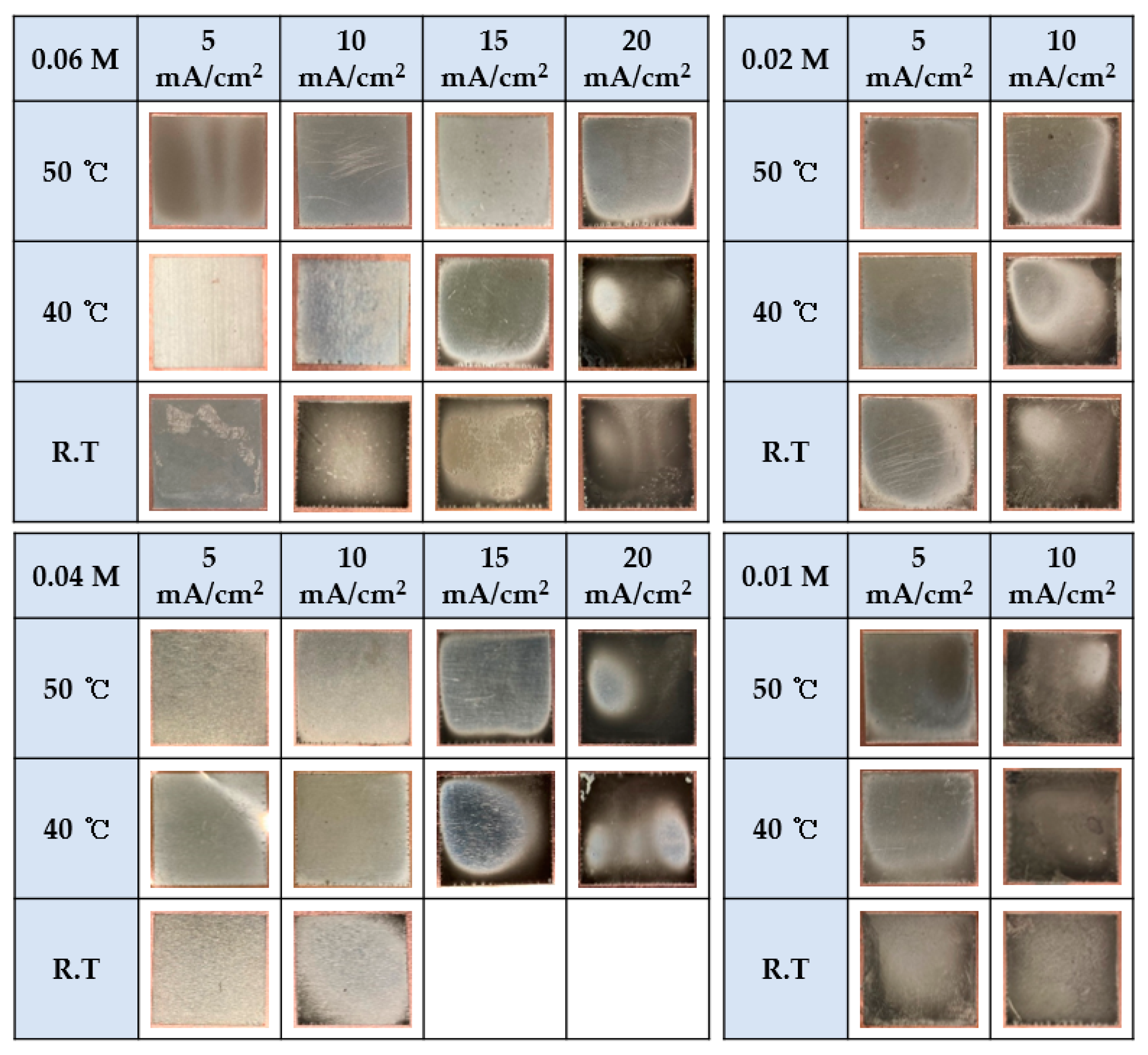
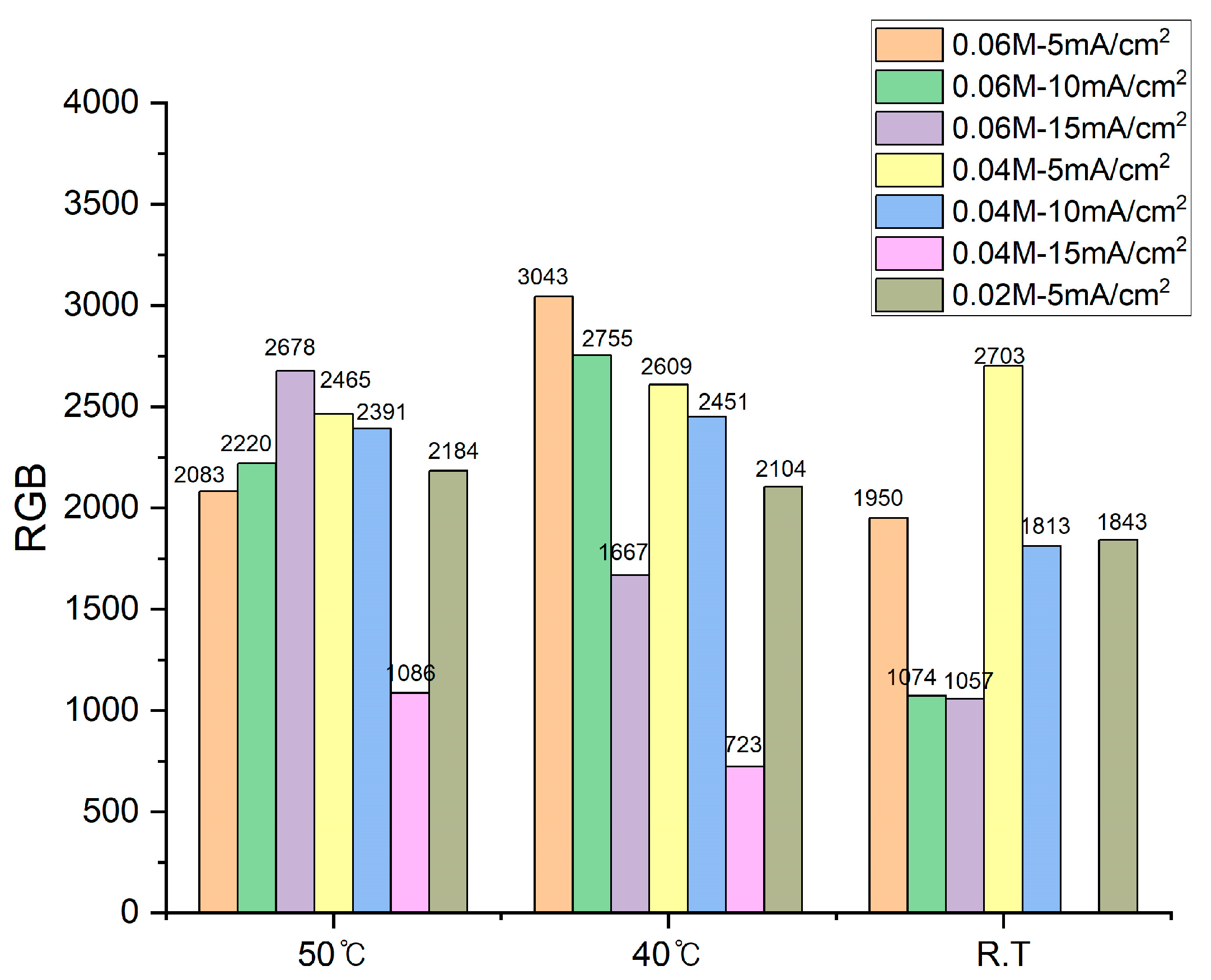
3.2. Evaluate Electroplating Quality

The sum of the RGB values of the samples shown in Figure 3 is shown in Figure 4. The best plating results were obtained at 5 mA/cm2 at 0.06 M and 40 °C, followed by plating at 10 mA/cm2. Comparing the results at 15 mA/cm2 to the results at 0.06 M at 50 °C, it can be seen that the quality of the plating improved as the solution temperature increased. At 15 mA/cm2, the higher temperature of the plating solution gave good results, while at 5 to 10 mA/cm2, the quality of the results at 40 °C was better than those at 50 °C.

3.3. SEM and EDS

To analyze the surface morphology of the nickel, the polished samples were examined via scanning electron microscopy (SEM, SU-5000; Hitachi, Tokyo, Japan) and energy-dispersive spectroscopy (EDS, X-MAX; Oxford, Oxford, UK). The samples shown in Figure 5 are SEM images of nickel-plated surfaces depending on the concentrations at a solvent temperature of 40 °C and a current density of 5 mA/cm2. The concentrations of (a) 0.06 M, (b) 0.04 M, and (c) 0.02 M led to uniform plating, while (d) 0.01 M showed cracks. This occurred because the size and shape of the particles were irregular during electroplating. As electroplating proceeds at a lower concentration, the current distribution on the cathode surface is irregular and the nickel crystal growth increases on the surface of the substrate when a higher current density is applied. Thus, dendrite crystals are formed [28].
In Figure 6, the cross-section of the 0.06 M, 5 mA/cm2, 40 °C sample with the best plating result is compared via SEM with that of the 0.04 M, 10 mA/cm2, 40 °C sample, which is the last condition without burnt plating or pitting. At 0.06 M, the most abundant concentration of Ni ions, the plating thickness was about 1.8 μm. In contrast, at 0.04 M, there was a slight decrease in the thickness, resulting in a plating thickness of 1.74 μm. The targeted thickness of 2 μm was not reached due to the lower concentration, resulting in lower cathodic current efficiency.
The cross-section of the sample plated under optimal conditions was measured using XRD and is shown in Figure 7. The results indicated only pure Ni was plated onto Cu, and it was also reconfirmed that the thickness of Ni was approximately 1.6 μm.

3.4. XRD

X-ray diffraction (XRD, Miniflex 600; Rigaku, Tokyo, Japan) was used to confirm the configuration and crystal structure of plating materials. Copper 2θ peaks (111), (200), and (220) were present in all samples, attributable to the copper substrate peaks. In addition, nickel 2θ peaks (111), (200), and (220) were found under all concentration conditions, thereby confirming that only nickel was electroplated. Furthermore, as shown in Figure 8, the higher the concentration, the lower the copper peak and the higher the nickel peak.
The X-ray diffraction (XRD) results can be utilized to measure the size of the crystals. By substituting the values from Table 2 into the Scherrer Equation (2), it is possible to calculate the lattice sizes for different concentrations [29,30]. The measurement range was set to range from 40 to 80 degrees, and all measured samples were fabricated at a current density of 5 mA/cm2 and temperature of 40 °C.
S i z e   D = 0.9 × λ β × cos θ ,
Size D represents the lattice size of the crystallite. λ is the filter value of K-beta used in XRD (1.39225 Å). β is the radian value of the full width at half maximum (FWHM) measured in degrees, and θ is 1/2 the value measured in 2θ. Table 2 presents the XRD data values for electroplated samples prepared at different concentrations. Based on the values from Table 2, the calculated lattice sizes are 55.06 nm for a concentration of 0.02 M, 47.46 nm for 0.04 M, and finally, 34.71 nm for 0.06 M. These findings show that the lattice size decreases as concentration increases.

4. Conclusions

In this study, optimal plating conditions and limit conditions were derived using a small plating bath designed for plating radioactive materials. An evaluation of the quality after electroplating showed that plating in the 0.06 M solution at a temperature of 40 °C with a current density of 5 mA/cm2 produced the most optimal quality. The limit condition for usable samples was a 0.04 M solution at 40 °C with a current density of 10 mA/cm2. When electroplating was performed under the optimal and marginal conditions, the thickness confirmed using SEM and EDS was approximately 1.8 to 1.60 μm. This experiment was performed using an insoluble anode, meaning that Ni ions were limited. The goal was to achieve a plating thickness of 2 μm, and approximately 80%–90% of the target thickness was achieved. This is because as plating progresses, the Ni ion concentration in the solution decreases, which results in a decrease in cathode current efficiency. When calculated using the density of nickel, the mass increase in the plating was 6.3 mg on average, and the thickness of the plating was 1.7 μm on average. The use of XRD confirmed that the higher the concentration, the more regularly the Ni ions were plated and the smaller the size of the crystals. It is expected that the appropriate plating thickness can be obtained based on the results above when conducting electroplating using nickel-63 in the future, and it is expected that this strategy can be applied to beta cells, random number generators, and other devices.

Author Contributions

Conceptualization, G.K., J.K. (Jin Kim) and S.K.; methodology, J.K. (Jongbum Kim); software, J.K. (Jongbum Kim); formal analysis, G.K. and J.K. (Jin Kim); investigation, J.K. (Jinjoo Kim); resources, J.H.; data curation, G.K.; writing—original draft preparation, G.K.; writing—review and editing, J.K. (Jin Kim) and S.K.; supervision, J.H.; project administration, S.K.; funding acquisition, J.K. (Jinjoo Kim). All authors have read and agreed to the published version of the manuscript.

Funding

This research was funded by the Korea Research Institute for defense Technology planning and advancement (KRIT) grant funded by the Korea government (DAPA (Defense Acquisition Program Administration)) (17-102-407-042(KRIT-CT-22-033)), Development of Betavoltaic battery technology for unmanned weapon system in extreme environments.

Institutional Review Board Statement

Not applicable.

Informed Consent Statement

Not applicable.

Data Availability Statement

Data are contained within this article.

Conflicts of Interest

The authors declare no conflicts of interest.

References

  1. Mohammadpour, Z.; Zare, H.R. Improving the Corrosion Resistance of the Nickel–Tungsten Alloy by Optimization of the Electroplating Conditions. Trans. Indian Inst. Met. 2020, 73, 937–944. [Google Scholar] [CrossRef]
  2. Bai, A.; Hu, C.C. Effects of electroplating variables on the composition and morphology of nickel–cobalt deposits plated through means of cyclic voltammetry. Electrochim. Acta 2002, 47, 3447–3456. [Google Scholar] [CrossRef]
  3. Sakti, A.R.; Riandadari, D.; Zakiyya, H.; Prapanca, A. The Effect of Process Variables on Work Piece Thickness and Glossiness from Metal Coating in Nickel-Chrome Metal Coating Process. IOP Conf. Ser. Mater. Sci. Eng. 2019, 494, 012057. [Google Scholar] [CrossRef]
  4. Giurlani, W.; Zangari, G.; Gambinossi, F.; Passaponti, M.; Salvietti, E.; Benedetto, F.D.; Caporali, S.; Innocenti, M. Electroplating for Decorative Applications: Recent Trends in Research and Development. Coatings 2018, 8, 260. [Google Scholar] [CrossRef]
  5. Cao, F.; Wang, J.; Lian, Y.; Wang, Y.; Wang, X.; Wang, X.; Song, A.; Shi, L. A Study on the Influence of the Electroplating Process on the Corrosion Resistance of Zinc-Based Alloy Coatings. Coatings 2023, 13, 1774. [Google Scholar] [CrossRef]
  6. Seritan, M.P.; Gutt, S.; Gutt, G.; Cretescu, I.; Cojocaru, C.; Severin, T. Design of experiments for statistical modeling and multi-response optimization of nickel electroplating process. Chem. Eng. Res. Des. 2011, 89, 136–147. [Google Scholar] [CrossRef]
  7. Tsuru, Y.; Nomura, M.; Foulkes, F. Effects of chloride, bromide and iodide ions on internal stress in films deposited during high speed nickel electroplating from a nickel sulfamate bath. J. Appl. Electrochem. 2000, 30, 231–238. [Google Scholar] [CrossRef]
  8. Fenimore, D.C.; Davis, C.M. Linear Electron Capture Detection. J. chromatog. Sci. 1970, 8, 519–523. [Google Scholar] [CrossRef]
  9. Dash, A.; Udhayakumar, J.; Kumar, M.; Shukla, R.; Gandhi, S.S.; Tyagi, A.K.; Venkatesh, M. Development of a micro electrochemical cell for in-situ deposition of 63Ni for use in electron capture detector (ECD) in gas chromatography. Radiochim. Acta 2011, 99, 733–741. [Google Scholar] [CrossRef]
  10. Munson, C.E., IV; Arif, M.; Streque, J.; Belahsene, S.; Martinez, A.; Ramdane, A.; Gmili, Y.E.; Salvestrini, J.P.; Voss, P.L.; Ougazzaden, A. Model of Ni-63 battery with realistic PIN structure. J. Appl. Phys. 2015, 118, 105101. [Google Scholar] [CrossRef]
  11. Kim, J.J.; Choi, S.M.; Son, K.J.; Hong, J.T. Manufacturing of Ni-63 Sealed Source for Betavoltaic Battery Using the Small-scale Electroplating Device. J. Radiat. Industry 2017, 11, 173–179. [Google Scholar]
  12. Tang, X.; Ding, D.; Liu, Y.; Chen, D. Optimization design and analysis of Si-63Ni betavoltaic battery. Sci. china. Tech. Sci. 2012, 55, 990–996. [Google Scholar] [CrossRef]
  13. Park, K.H.; Park, S.M.; Choi, B.G.; Kim, J.B.; Son, K.J. High rate true random number generator using beta radiation. AIP Conf. Proc. 2020, 2295, 020020. [Google Scholar]
  14. Kretowicz, M.N.; Barrett, K.E.; Barnhart, T.E.; Engle, J.W. Recycling of 52Cr electroplated targets for 52gMn production. Appl. Radiat. Isot. 2023, 200, 110924. [Google Scholar] [CrossRef] [PubMed]
  15. de Souza, C.D.; Kim, J.B.; Kim, J.J.; Kim, J.; Ji, W.O.; Son, K.J.; Choi, S.M.; Kang, G.J.; Hong, J.T. Monte Carlo simulation for evaluating the attenuation effects of a protective layer for a Ni-63 nuclear battery. Prog. Nucl. Energy 2022, 144, 104084. [Google Scholar] [CrossRef]
  16. Gui, G.; Zhang, K.; Blanchard, J.P.; Ma, Z. Prediction of 4H-SiC betavoltaic microbattery characteristics based on practical Ni-63 sources. Appl. Radiat. Isot. 2016, 107, 272–277. [Google Scholar] [CrossRef]
  17. Mandich, V.; Baudrand, D.W. Troubleshooting Electroplating Installations: Nickel Sulfamate Plating Systems. Plat. Surf. Finish. 2002, 89, 68–76. [Google Scholar]
  18. Li, D.; Zhang, P.; Wu, Y.H.; Liu, Y.S.; Xuan, M. Uniformity study of nickel thin-film microstructure deposited by electroplating. Microsyst. Technol. 2009, 15, 505–510. [Google Scholar] [CrossRef]
  19. Sun, Y.T.A.; Liu, M.C.; Zhang, Y.; Huang, Y.P.; Chen, W.E. Development of an electrolyte jet type apparatus for manufacturing electroplated diamond wires. Precis. Eng. 2021, 68, 351–357. [Google Scholar]
  20. Mandich, N.V. Troubleshooting decorative electroplating installations—Part 3: Pores, spotting-out, pits, peeling & blistering. Plat. Surf. Finish 2000, 87, 74–79. [Google Scholar]
  21. Rose, I.; Whittington, C. Nickel Handbook; Nickel Institute: Toronto, ON, Canada, 2014. [Google Scholar]
  22. Prioyono, T.; Haftirman, H.; Kholil, M.; Zainal, F.F.; Salleh, M.A.A.M. Effect of electroplating process time on medal antique gold colour of zinc alloy material. In AIP Conference Proceedings; AIP Publishing: College Park, MD, USA, 2020; Volume 2291, p. 020060. [Google Scholar]
  23. Albizu, G.; Bordagaray, A.; Davila, S.; Garcia-Arrona, R.; Ostra, M.; Vidal, M. Analytical control of nickel coating baths by digital image analysis. Microchem. J. 2020, 154, 104600. [Google Scholar] [CrossRef]
  24. Vidal, M.; Amigo, J.M.; Bro, R.; Berg, F.V.D.; Ostra, M.; Ubide, C. Image analysis for maintenance of coating quality in nickel electroplating baths–Real time control. Anal. Chim. Acta 2011, 706, 1–7. [Google Scholar] [CrossRef] [PubMed]
  25. Gamburg, Y.D.; Zangari, G. Theory and Practice of Metal Electrodeposition; Springer: Berlin/Heidelberg, Germany, 2011. [Google Scholar]
  26. Cziraki, A.; Fogarassy, B.; Gerocs, I.; Toth-Kadar, E.; Bakonyi, I. Microstructure and growth of electrodeposited nanocrystalline nickel foils. J. Mater. Sci. 1994, 29, 4771–4777. [Google Scholar] [CrossRef]
  27. Stroumbouli, M.; Gyftou, P.; Pavlatou, E.A.; Spyrellis, N. Codeposition of ultrafine WC particles in Ni matrix composite electrocoatings. Surf. Coat. Technol. 2005, 195, 325–332. [Google Scholar] [CrossRef]
  28. Ning, Z.; He, Y.; Gao, W. Mechanical attrition enhanced Ni electroplating. Surf. Coat. Technol. 2008, 202, 2139–2146. [Google Scholar] [CrossRef]
  29. Holder, C.F.; Schaak, R.E. Tutorial on Powder X-ray Diffraction for Characterizing Nanoscale Materials. ACS Nano 2019, 13, 7359–7365. [Google Scholar] [CrossRef]
  30. Scherrer, P. Bestimmung der Grosse und inneren Struktur von Kolloidteilchen mittels Rontgenstrahlen. Nach Ges Wiss Gott. 1918, 2, 8–100. [Google Scholar]
Figure 1. (a) Small electroplating bath and (b) the components of a small electroplating system.
Coatings 14 00613 g001
Figure 2. Amount of beta particles emitted from the surface per nickel-63 plating thickness.
Coatings 14 00613 g002
Figure 3. Plated surface results for each concentration according to the temperature and current.
Coatings 14 00613 g003
Figure 4. Comparison of the sum of five points of RGB values from samples plated under different conditions.
Coatings 14 00613 g004
Figure 5. Plated surface appearance due to concentration differences of (a) 0.06 M, (b) 0.04 M, (c) 0.02 M, and (d) 0.01 M.
Coatings 14 00613 g005
Figure 6. A cross-section of Ni plating at (a) 0.06 M, 40 °C, 5 mA/cm2 and (b) 0.04 M, 40 °C, 10 mA/cm2 was examined using SEM to determine the plated thickness.
Coatings 14 00613 g006
Figure 7. EDS was used to map the distributions of Ni and Cu.
Coatings 14 00613 g007
Figure 8. XRD data measured after Ni plating on a copper plate at 0.06 M, 0.04 M, and 0.02 M.
Coatings 14 00613 g008
Table 1. Operational conditions of each sandpaper type used for polishing.
Carbon Sheet ThicknessLubricantAbrasivePlaten SpeedHead SpeedPressureMinutes
400 gritWaterSiC sandpaper60150337
600 grit
800 grit3510
1200 grit
1500 grit
6 μmPolycrystalline Diamond suspensionPolishing cloth385
1 μm40
Table 2. XRD data for electroplated samples fabricated at different concentrations.
ConcentrationθFWHM (deg)FWHM (rad)Size (Å)
0.02 M50.76125.38040.1440.002519550.6
0.04 M50.57625.28780.1670.002920474.6
0.06 M50.71325.35650.2290.003995347.1
Disclaimer/Publisher’s Note: The statements, opinions and data contained in all publications are solely those of the individual author(s) and contributor(s) and not of MDPI and/or the editor(s). MDPI and/or the editor(s) disclaim responsibility for any injury to people or property resulting from any ideas, methods, instructions or products referred to in the content.

