Review

On Numerical Modelling and an Experimental Approach to Heterojunction Tandem Solar Cells Based on Si and Cu2O/ZnO—Results and Perspectives

by
Laurentiu Fara
1,2,*,
Irinela Chilibon
3,
Ileana Cristina Vasiliu
3,*,
Dan Craciunescu
1,
Alexandru Diaconu
1 and
Silvian Fara
1
1
Department of Physics, Faculty of Applied Sciences, National University of Science and Technology POLITEHNICA Bucharest, Splaiul Independentei 313, RO-060042 Bucharest, Romania
2
Academy of Romanian Scientists, 3 Ilfov, RO-050044 Bucharest, Romania
3
National Institute of Research and Development for Optoelectronics (INOE-2000), 409 Atomistilor Street, RO-077125 Magurele, Romania
*
Authors to whom correspondence should be addressed.
Coatings 2024, 14(3), 244; https://doi.org/10.3390/coatings14030244
Submission received: 28 November 2023 / Revised: 29 December 2023 / Accepted: 18 February 2024 / Published: 20 February 2024

Abstract

:
A comparative analysis of three advanced architectures for tandem solar cells (SCs) is discussed, respectively: metal oxide, thin film, and perovskite. Plasmonic solar cells could further increase solar cell efficiency. Using this development, an innovative PV technology (an SHTSC based on metal oxides) represented by a four-terminal Cu2O/c-Si tandem heterojunction solar cell is investigated. The experimental and numerical modelling study defines the main aim of this paper. The experimental approach to SHTSCs is analysed: (1) a Cu2O layer is deposited using a magnetron sputtering system; (2) the morphological and optical characterization of Cu2O thin films is studied. The electrical modelling of silicon heterojunction tandem solar cells (SHTSCs) is discussed based on five simulation tools for the optimized performance evaluation of solar devices. The main novelty of this paper is represented by the following results: (1) the analysis suggests that the incorporation of a buffer layer can improve the performance of a tandem heterojunction solar cell; (2) the effect of interface defects on the electrical characteristics of the AZO/Cu2O heterojunction is discussed; (3) the stability of SHTSCs based on metal oxides is studied to highlight the degradation rate in order to define a reliable solar device. Perspectives on SHTSCs based on metal oxides, as well as Si perovskite tandem solar cells with metal oxides as carrier-selective contacts, are commented on.

1. Introduction

A solar cell, or a photovoltaic (PV) cell, is an electrical device that converts light energy directly into electricity by the photovoltaic effect. The operation of a photovoltaic (PV) cell requires three essential features: (a) the absorption of light, generating electron–hole pairs; (b) the separation of charge carriers of opposite types; and (c) the separate extraction of those carriers to an external circuit.
There are different types of solar cells: (1) amorphous silicon (A-Si) solar cells; (2) biohybrid solar cells (which are based on a combination of organic and inorganic matter); (3) silicon buried-contact solar cells; (4) cadmium telluride solar cells; (5) concentrated PV (CPV) cells; (6) copper indium gallium selenide (CIGS) solar cells; (7) dye-sensitized solar cells (DSSCs); (8) gallium arsenide solar cells (GaAs SCs); (9) hybrid polymer solar cells (HPSCs); (10) luminescent solar concentrator cells (LSCCs); (11) monocrystalline silicon solar cells (Mono-Si SCs); (12) polycrystalline silicon solar cells (Poly-Si SCs); (13) multijunction solar cells (MJSCs); (14) quantum dot solar cells (QDSCs); (15) tandem solar cells (TSCs).
Tandem solar cells could have a very good conversion efficiency in comparison with other types of solar cells. Tandem solar cells use two different materials that absorb solar radiation; this means that a tandem solar cell can absorb more of the solar spectrum—and so produce more electricity—than if one material is used (such as silicon solar cells).
Tandem solar cells are considered the industry’s next step in photovoltaics due to their excellent conversion efficiency. A very good example is the perovskite absorber material that has been developed for efficient tandem solar cells. The European Solar Test Installation has verified a 32.5% efficiency for perovskite/silicon tandem solar cells.
The paper studies solutions related to tandem solar cells based on silicon, using three advanced architectures with different material structures, namely, metal oxide, thin film, and perovskite [1,2].

1.1. Metal Oxide Tandem Heterojunction Solar Cells

Currently, more than 90% of the photovoltaic (PV) market is dominated by crystalline Si solar cells [3]. Silicon-based tandem heterojunction solar cells having a metal-oxide subcell represent an attractive approach in the development of the next generation of SCs.
Cutting the cost of PV-producing technology would be possible if low-cost metal oxides were used in fabrication of Si-based tandem solar cells to be developed further.
Cuprous oxide (Cu2O), as a p-type semiconductor with high optical absorption and a direct bandgap of about 2.1 eV, is suggested to be a good match for PV applications. A p-n heterojunction could be designed and fabricated using an n-type semiconductor such as ZnO. As both TiO2 and ZnO are low-cost oxides, the premises to develop a low-cost heterojunction solar cell are met. Since only 8% conversion efficiency has been achieved experimentally to date [4,5], further investigation of Cu2O-based solar cells could create the premises to fully achieve the potential of PV technology, as it is known that the maximum theoretical efficiency of such SCs is 19% [6,7].
Three different versions of flexible ZnO/Cu2O solar cells have been developed, respectively: (1) thin film; (2) nanowire; and (3) nanotube [8]. ZnO nanowires and nanotubes are implied to have higher efficiency than thin films, at about 0.12%. ZnO thin films have relatively low efficiency of 0.02%.
The key limitations of the power conversion efficiency (PCE) of a metal oxide SHTSC are given by three factors: material and charge collector quality, material absorption coefficient, and interface quality. Thus, special efforts must be made to understand SHTSC behaviour and the most important parameters for achieving optimum performance.

1.2. III–V Tandem Solar Cells

A III–V tandem SC with 6 junctions is characterized by an efficiency of 47.1% under concentrated solar irradiance [9]. Tandem SCs using Si as a bottom cell, with a high efficiency, are classified conceptually as III–V/Si. For the cases of 2-junction GaAs/Si SC, and 3-junction GaInP/GaAs/Si SC the maximum efficiency values obtained are 32.8% and 35.9%, respectively.
New investigations have shown an increased efficiency for 2-junction and 3-junction SCs designed by direct growth technology. At the same time, smart stacking technology confers a significant efficiency advantage. It has been noted that the cost of a Si-based III–V tandem SC is lower than that of a III–V tandem SC. The usual degradation conditions are defined by heat, moisture, oxygen, and UV radiation, leading to long-term stability. Thus, Si-based III–V tandem SCs are very stable and reliable.

Plasmonic Solar Cells

An improved approach of increased efficiency for SHTSCs based on metal oxides can be applied for III–V tandem SCs by incorporating plasmonic nanocomponents [10]. Due to their ability to scatter light back into the PV structure and their low absorption, plasmonic nanoparticles are studied as a method for increasing solar cells’ efficiency [10,11,12].
The plasmons excited by optical radiation induce an electric current from hot electrons in materials made from gold particles and light-sensitive molecules of porphin. The wavelength to which the plasmon responds is a function of the size and distance between particles. The material is made by ferroelectric nanolithography. Compared to conventional photoexcitation, the material produces three to ten times the current [13,14]. The same idea applies to the discussion of perovskite tandem SCs [15].
Metallization is performed on doped regions at either low or high temperatures. Low-temperature metal contacts can be made in Ni/Si, ITO/a-Si, or ITO/Si configurations. High-temperature metallization is based on screen printing and simultaneous annealing of Al (positive) and Ag (negative) paste contacts in a conveyor-belt furnace as it transits across multiple temperature zones.

1.3. Perovskite Tandem Solar Cells

The highest verified efficiency obtained for perovskite tandem SCs to date is 29.15% [11]. Rapid improvements have been made for tandem perovskite/Si-based SCs, with the advantage of much lower cost. For perovskite/Si solar cells, the laboratory performance record achieved is 32.5%. Most of the existing high-efficiency perovskite tandem SCs are technologically acceptable for low-cost SCs; specifically, the estimated cost of perovskite SCs is one-third of the cost of Si SCs. In contrast, the long-term stability of perovskite/Si-based SCs is low because moisture causes deterioration of its performance. Therefore, special efforts are needed to prevent this degradation. Perovskite SCs have shorter lifetimes, ranging from a few days to months and up to a year at most. It is imperative to study, develop and test a long-life perovskite tandem SC. For perovskite SCs, the requirements are increases in efficiency and long-term stability, along with reductions in manufacturing costs. However, there have been promising approaches for simultaneously achieving higher efficiency and stability. As perspective, there is much more open potential for the coming years.

2. The Article’s Structure, Methodology, and Novelty

The main purpose of this review study is determined by the experimental and numerical simulated investigation of an advanced metal oxide (based on Cu2O and ZnO) silicon tandem solar cell.
The article’s structure is based on the following plan of development:
(1)
The introduction discusses three advanced architectural solutions with different material for tandem solar cells;
(2)
The fundamental idea of the analysed SHTSCs based on Cu2O and ZnO metal oxides is presented;
(3)
The experimental approach is represented by the following items: (a) deposition of Cu2O thin films with a sputtering system, (b) morphological and optical characterization of Cu2O thin films, and (c) physical parameters of Cu2O thin films;
(4)
Numerical modelling: (i) five main simulation software tools for the top and bottom subcells are discussed; (ii) experimental and simulated EQE and J–V curves are studied; (iii) interface defects are analysed;
(5)
The stability and reliability of silicon heterojunction tandem solar cells (SHTSCs) is discussed;
(6)
Conclusions and perspectives are highlighted.
The methodology of the article is highlighted by five essential SC-related items: (1) fabrication, (2) characterization, (3) numerical simulation, (4) IDL analysis, and (5) stability and reliability.
The main novelty of this study is determined by the analysis of the performance improvement of SHTSCs based on a specific buffer-layer introduction and the control of interface defects, as well as reducing the degradation rate for a reliable solar device.

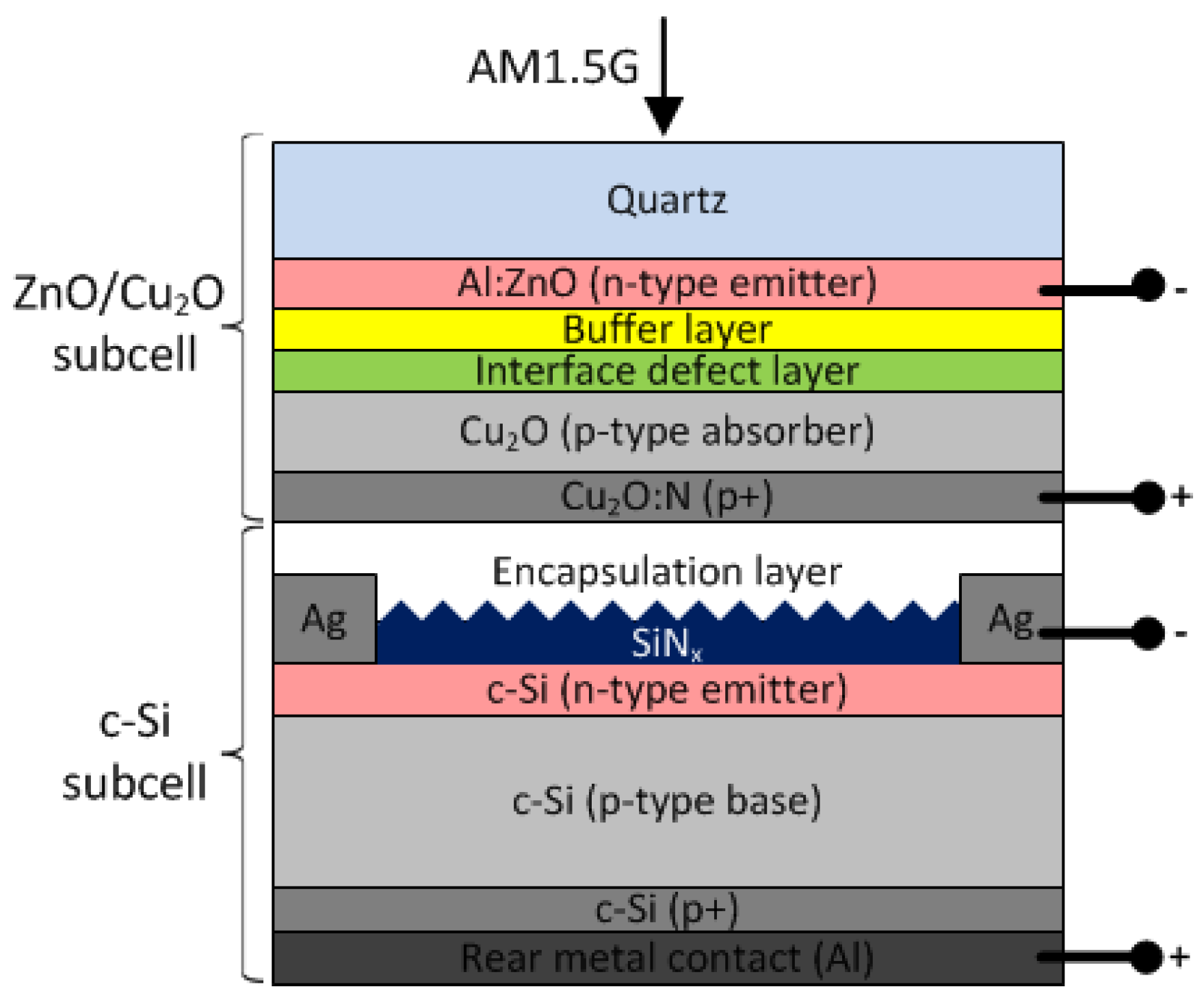
3. The Fundamental Idea of SHTSCs

The tandem solar cell is composed of (i) a top subcell formed from an Al-ZnO/Cu2O heterojunction and (ii) a bottom subcell based on c-Si (Figure 1). The visible-light transparency and the electrical conductivity of the ZnO layer are improved as a result of Al doping. That is why an Al-doped ZnO layer would represent a promising transparent conducting electrode for nano-optoelectronic solar devices [16].
The proposed approach aims at increasing of the power efficiency beyond the conventional limit of the Si solar cell. Through the top subcell, the low-energy photons are transmitted, while through the bottom subcell, the high-energy photons are absorbed (Figure 2). Thus, a 4-terminal configuration for the tandem solar device was determined because the current density of the top subcell is half that of the bottom subcell.
A layer of cuprous oxide (Cu2O) can act as a photoabsorber [6,7,8,9,17]. Cu2O is preferred due to the following main merits: (1) it is present in great quantities on earth; (2) it has reduced toxicity, and (3) it has low costs of synthesis. The main characteristics that qualify it for photovoltaic applications are the following: (1) Cu2O is a p-type semiconductor; (2) its bandgap is Ego = 2.1 eV; (3) it has a high absorption coefficient of 105 cm−1; (4) its absorption edge is sharp; (5) it has a high carrier mobility (100 cm2 V−1 s−1); (6) the electron affinity is low (3.2 eV); (7) it has band offsets with an n-type heterojunction partner; (8) the heat of formation is low (−171 kJ/mol); and (9) the interface is prone to oxidation and formation of an interface defect layer (IDL). Theoretically, the conversion efficiency of the copper oxide layer is 19%, but experimentally, a maximum conversion efficiency of only 8% has been obtained.

4. SHTSC Experimental Approach: Deposition, Characterization, and Physical Parameters of Cu2O Films

4.1. Cu2O Films Deposition by a Sputtering System

A magnetron sputtering method was used to deposit Cu2O films on a quartz substrate [18,19,20,21,22]. The Cu target was placed in O2/Ar, and the substrate temperature was kept at 400 °C. Cu2O films with a thickness of around 500 nm were deposited at a rate of ~25 nm/min, then further annealed at 900 °C and p~0.1 Torr for 3 min.
An Al-doped ZnO layer was deposited by co-sputtering of a 99.99% ZnO target and a 99.999% Al target in an Ar atmosphere using a 400 °C substrate temperature.
The proposed architecture of a silicon tandem heterojunction solar cell (SHTSC) formed by sputtering deposition of metal oxides is presented in Figure 1. The device allows an increase in conversion efficiency by using two solar subcells connected in series.
This innovative solution would contribute to the achievement of an improved solar cell by using low-cost materials and non-toxic metal oxides, which remove the disadvantages of conventional solar cells.

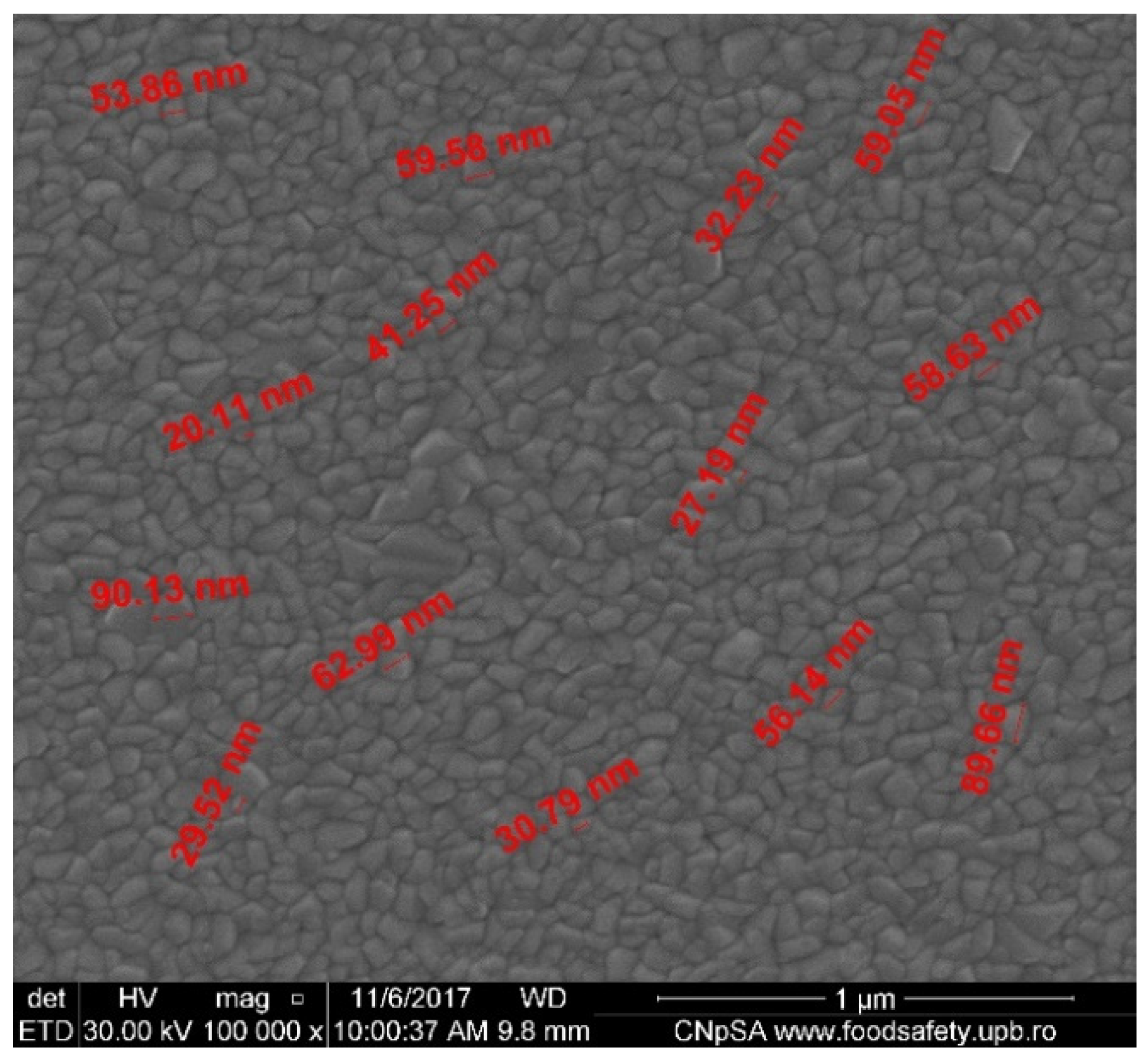
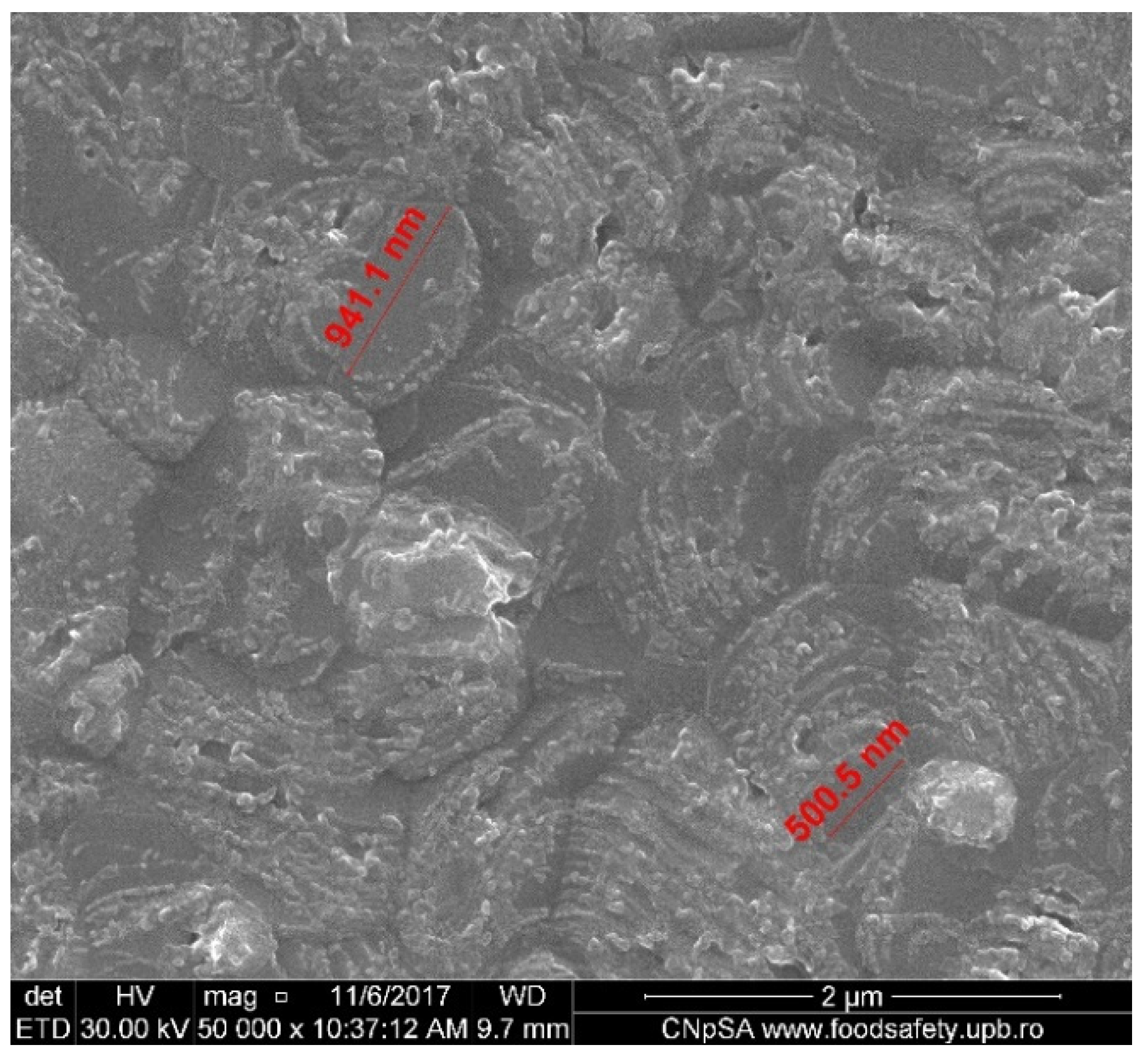
4.2. Morphological Characterization of Cu2O Films

A scanning electron microscope (SEM) equipped with an electron emission gun was used to investigate the morphology of the Cu2O film samples [22,23] with a resolution of 1.2 nm.
The average grain size increased after the annealing, as noticed from the SEM images of 500 nm thick Cu2O coatings as grown (Figure 3) and annealed at 900 °C (Figure 4).
At the same time the samples were analysed using an atomic force microscope (AFM), with a Si-doped probe. It was noted that the surface roughness RRMS for the as-grown Cu2O coatings deposited on quartz increases after annealing at 900 °C for 3 min in vacuum, and the largest RRMS reaches about 21 nm the largest RRMS [23].

4.3. Optical Characterization of Cu2O Films

The X-ray fluorescence measurements were carried out using an XRF material analyser [24]. An ellipsometer in the wavelength range of 190 to 2100 nm allowed the determination of the film thickness and complex refractive index [25,26]. Delta psi was the model used to fit the measured ellipsometry parameters.
It was noticed that the optical transmittance properties of the Cu2O films were improved in the Vis and near-IR wavelength range after annealing, which is likely to be due to the larger grain size and a corresponding reduction in grain-boundary scattering, possibly together with less strained film (Figure 5) [22,27].
It was suggested that the effect of broadening of the optical band gap after annealing might be due to partial elimination of defects and possibly to less contaminated Cu2O films. In this way, the optical band gap increases from Eg = 2.06 eV for as-grown Cu2O film to Eg = 2.19 eV after annealing at 900 °C.
The energy-dispersive X-ray spectroscopy (EDX) spectrum for Cu2O film of 500 nm thickness (Figure 6) revealed the composition of the film, namely, the net Cu/O gravimetric ratio of the sample. It is suggested that the gravimetric ratio of the Cu2O film deposited by magnetron sputtering is Cu/O = 4:1, which means that there are mostly Cu2O compounds of high purity.

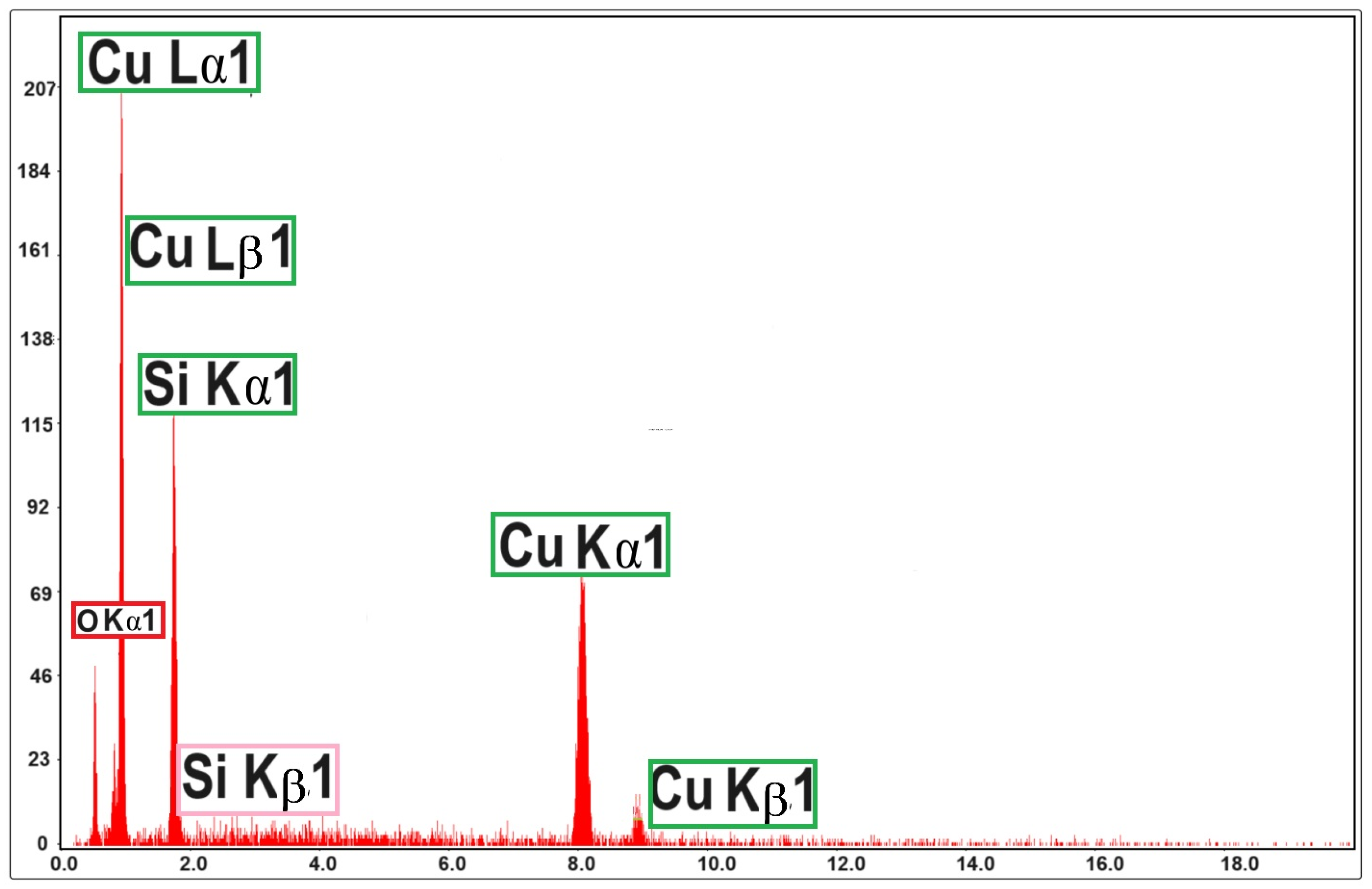
4.4. Physical Parameters of Cu2O Films

The measurements of the Hall effect at room temperature were carried out using the van der Pauw configuration. The room-temperature Hall effect measurements allowed the evaluation of hole mobility, film resistivity, and hole concentration for the 500 nm thick as-grown and annealed Cu2O films on quartz. The majority carrier (hole) mobility of the Cu2O coatings increased from 10 to 50 cm2 V−1 s−1 after annealing, and the resistivity decreased from 560 to 200 Ω·cm [28,29]. These values are comparable to those reported previously for sputter-deposited polycrystalline Cu2O films on quartz [21,30], which suggests that the annealed Cu2O thin films are well suited for photovoltaic applications. The increase in the carrier mobility after annealing could be attributed to the increase in grain size and reduced grain-boundary scattering.

5. SHTSC Numerical Modelling—Analysis of Interface Defects

5.1. Simulation Results for Electrical Modelling of SHTSC

The developed electrical model of an SHTSC device was based on five main simulation software tools: the first four, (a) Afors-Het 2.5.0 [31], (b) wxAMPS-2D, (c) Silvaco Atlas TCAD, and (d) AMPS-1D [32], were used for the Cu2O/ZnO top subcell, and (e) PC1D v5.9/Quokka 2 v FRC was used for the bottom c-Si subcell [5,26,32].
For the top subcell, simulation tools (a), (b), (c), and (d) were used in order to highlight those heterojunction properties that are involved in a high conversion efficiency of the studied SC. Reducing the defect density at the heterojunction interfaces of the SC could possibly prevent recombination losses. At the same time, ZnO determines a conduction band offset of roughly 0.9 eV for Cu2O, which produces a low open-circuit voltage (Voc).
The following interesting results based on the four simulation tools used for numerical modelling of the Cu2O/ZnO top subcell were noted:
(a)
The electrical modelling in Afors-Het solved the semiconductor equations, the Poisson equation, and the transport equation for electrons and holes by the finite-difference method. This structure was used to analyse the influence of doping for the component layers on the essential parameters of the top subcell;
(b)
In the simulation with wxAmps, a performance assessment of the metal oxide subcell was performed for optimized thicknesses of the Cu2O and ZnO layers taking into account the subcell’s electric parameters, respectively: the fill factor, the short-circuit current, the open-circuit voltage, and the conversion efficiency of the implemented solar device as a function of temperature;
(c)
The numerical model developed in Silvaco Atlas was a complex one that aimed to optimize the structure of the subcell but also the material parameters for its layers. Using Silvaco Atlas, several values for the doping level were simulated, respectively, at the level of defect density presented in the copper oxide subcell. Based on the obtained results, the electric parameters of the solar subcell were established for different values of defect density of the Cu2O layer;
(d)
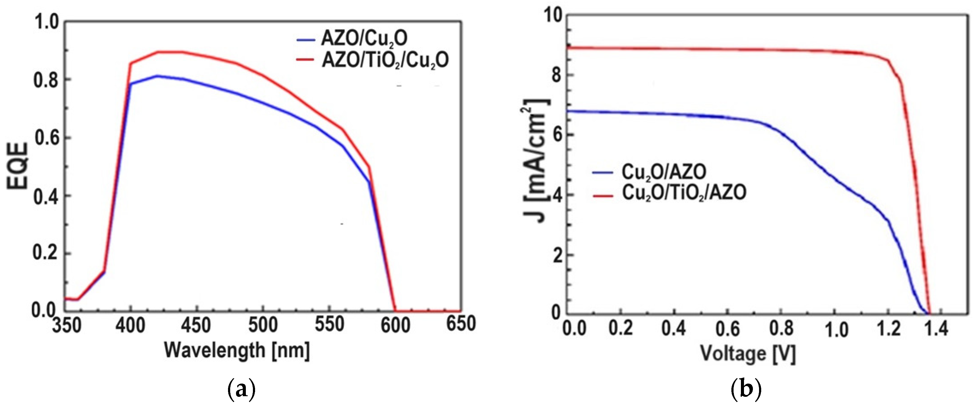
A titanium dioxide (TiO2) thin film can act as a buffer layer in a Cu2O/ZnO solar cell based on the following noticed properties: (1) high optical transparency; (2) good transport properties; and (3) a wide band gap. The effect of this buffer layer on the characteristics of ZnO/Cu2O SC was considered very important for improving the performance of such solar devices.
ZnO/Cu2O SCs with a TiO2 buffer layer were analysed by the AMPS-1D (Analysis of Microelectronic and Photonic Structures-1D) simulation software tool [32]. TiO2 behaved as an active material that absorbed photons and converted them into electric current, having a band gap around 3.2–3.8 eV, which allows the effective absorption of UV light [33,34]. The influence of TiO2 inclusion on the following SC characteristics, respectively, was considered: (1) the open-circuit voltage (Voc); (2) the short-circuit current (Jsc); (3) the SC conversion efficiency (η); and (4) the fill factor (FF). In order to obtain essential knowledge of SHTSC design, it is required to determine the optimized values of the SC physical parameters. The following parameters were investigated, respectively: (1) layer thickness, (2) doping density, and (3) defect density.
The AMPS-1D simulation software tool could be used to investigate the relationship between an SHTSC’s performance and its physical parameters. The effect of the buffer layer was analysed using the three input physical parameters selected from the literature. Unoptimized Cu2O/ZnO solar cells were employed as a benchmark for evaluation. The input physical parameters are presented in the Table 1.
The performance of AZO/Cu2O and AZO/TiO2/Cu2O SCs was investigated under AM1.5 solar illumination and at 300 K. The obtained simulation results are summarized in the Table 2, based on the literature-derived physical parameters given in Table 1. Two cases were studied:
A.
The simulated SHTSC without the TiO2 buffer layer presented the following SC output parameters: Voc = 0.65 V, Jsc = 7.81 mA cm−2, FF = 39.1%, and η = 2.54%. The obtained efficiency was in agreement with the experimental value of Minami et al. [19]; our work was used for comparison and analysis of the research on simulated SHTSC without and with the TiO2 buffer layer, respectively.
B.
A remarkable improvement was obtained by introducing the intermediate TiO2 buffer layer between ZnO/AZO and Cu2O. As a result, Voc, Jsc, FF, and η had the following values: 0.84 V, 8.74 mA cm−2, 50.4%, and 5.02%, respectively.
The meanings of the symbols are as follows: Jsc is short-circuit current density; Voc is open-circuit voltage; FF is fill factor; η is conversion efficiency.
Figure 7a,b exhibit the external quantum efficiency (EQE) and J–V simulation graphs for Cu2O/TiO2/AZO; they increase for the whole spectrum range with the addition of a TiO2 buffer layer [32]. Figure 8a,b exhibit experimental J–V plots, in the dark and light, before annealing and after annealing for a TiO2/Cu2O solar cell [37].
A TiO2 used as buffer layer of an AZO /Cu2O heterojunction solar cell was noted to lead to the highest efficiency. To optimise the solar-cell device performance, three parameters, namely, the thickness of the layer, the doping concentration, and the defect density, could provide improvements in the AZO/TiO2/Cu2O structure.
(e)
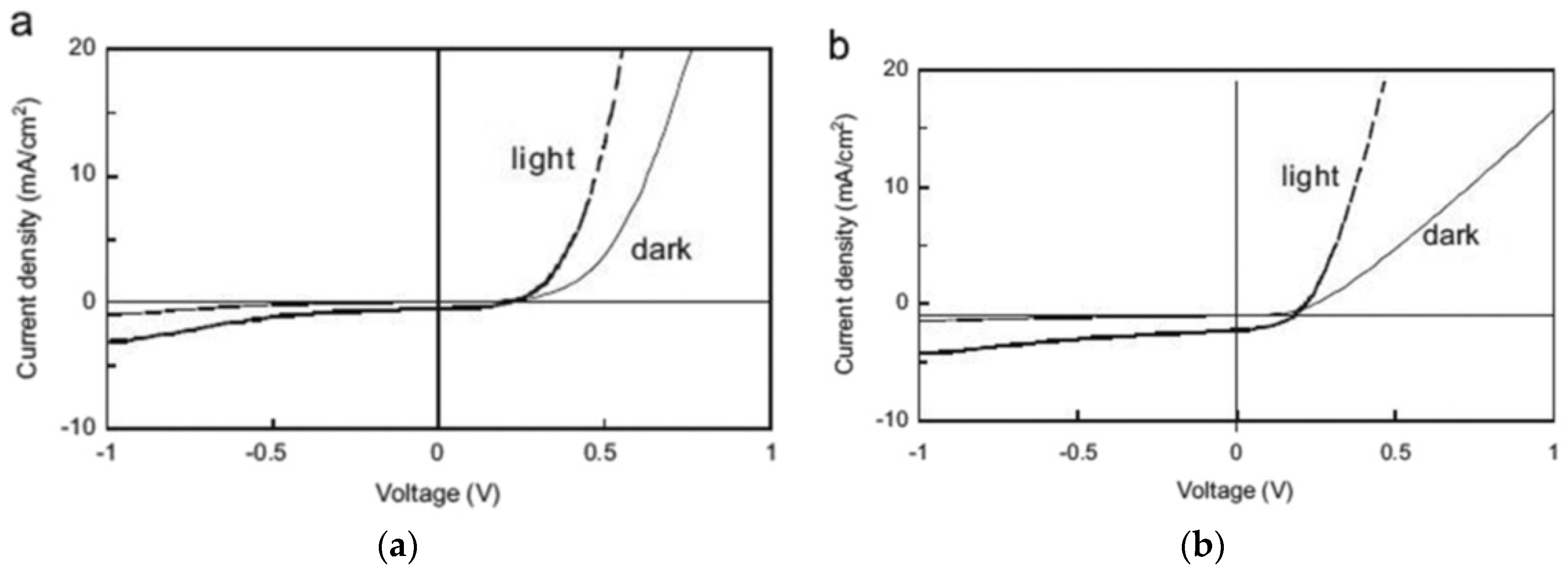
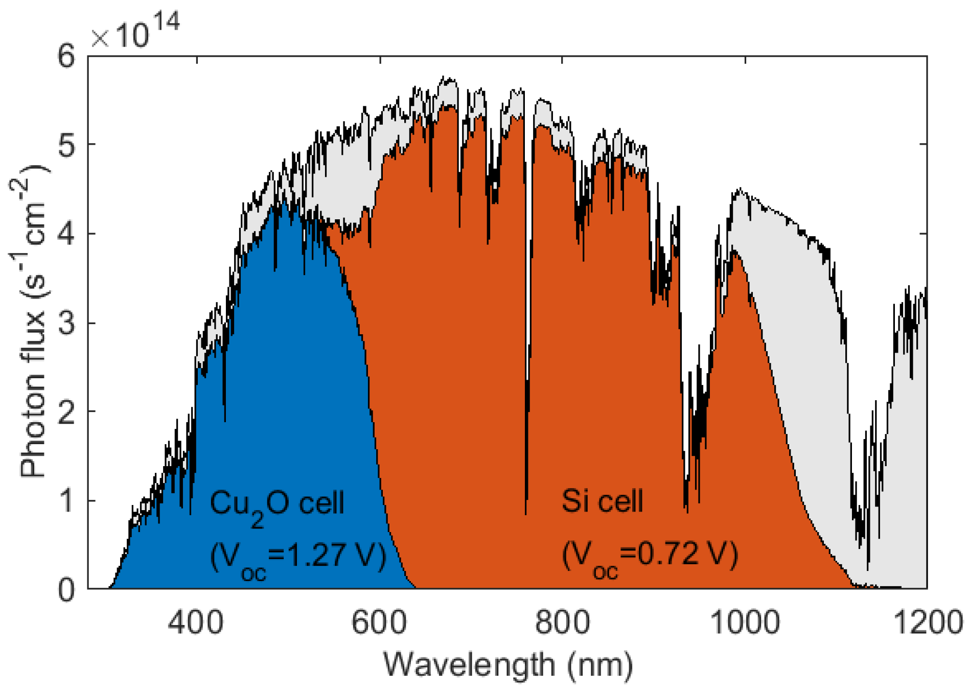
For the silicon bottom subcell, a numerical model was developed using the PC1D/Quokka 2 platform, and the model was then compared to the experimental plot [3,26,34]. Therefore, a predicted model of the Si subcell was established. Based on the model improvement, a simulated external quantum efficiency (EQE) plot was calculated to compare with the experimental EQE plot (Figure 9a). At the same time, the J–V graph was studied; it can be observed that the simulated graph is very close to the experimental one (Figure 9b).

5.2. Analysis of Interface Defects in SHTSCs

The real performance of SCs is very different from the theoretical evaluation. This situation occurs for three reasons: (i) impurities, (ii) defects, and (iii) interface states. Metal oxide materials used in SC production (respectively Cu2O and ZnO) are usually characterized by two essential features: (a) a very high density of defects and (b) a poor energy performance [34]. At the same time, the interface states generated by the mismatch between two different heterostructure materials can give rise to special problems, generated by recombination and tunnelling effects. Since recombination losses can reduce an SC’s optical performance, the study of interface defects is essential for a realistic approach to SHTSC modelling. To analyse the feasibility of a heterojunction based on copper and zinc oxides, the solar device should be numerically modelled taking into account the influence of defects and interface states [35,36,37,38,39,40,41].
The main simulation results regarding the interface defects can be synthesized as follows:
(1)
The SC electrical parameters were obtained based on the DD (defect density) of the IDL (interface defect layer) for different thicknesses.
The results indicated a significant reduction in the energy performance of the SHTSC for a DD in the IDL over 1019 cm−3, the IDL thickness being non-significative. That is why the normal thickness of the IDL layer could be established at 5 nm and the DD at 1018 cm−3.
(2)
The behaviour of the conduction-band energy for different DD values of the IDL (Figure 10a) could be studied. An important increase was observed in the bandgap between the buffer layer and the IDL for a DD above 1019 cm−3, resulting in decreased SC performance.
(3)
The parameters of the analysed SHTSC could be investigated according to the DD of the Cu2O layer in the SC.
(4)
The behaviour of the conduction-band energy for different Cu2O-layer acceptor concentrations could be studied (Figure 10b). There was a significant increase in the bandgap for a concentration above 1016 cm−3 that provoked an SC performance decrease.
(5)
The simulated results showed a significant decrease in SC performance for a DD of the Cu2O layer over 1013 cm−3. That is why the value of DD for the Cu2O layer was set at 1013 cm−3.

6. Stability and Reliability of Si Heterojunction Tandem Solar Cells (SHTSC)

Stability is an essential parameter of commercial silicon-based tandem heterojunction solar cells (SHTSC) with metal oxides and can improve its lifetime. For SC stability, it is necessary to minimize the influence of environmental parameters, such as humidity, UV, and temperature [7].
The degradation rates of SHTSCs depend on the characteristics of different structures and materials, such as porosity, temperature, and the intrusion of sodium ions (Na+) and moisture. For instance, H2 plasma treatment reduces porosity and improves SC stability.
The design stability of intrinsic hydrogenated Si, or H(i), films for SHTSCs is influenced by the intrusion of sodium ions (Na+) and moisture during Na+ testing, with degradation of the SCs’ efficiency [42].
According to the International Technology Roadmap for Photovoltaics (ITRP) [43], passivated emitter and rear solar cells (PERSCs) dominate the SC market. The effectiveness of improving the contact resistance of off-specification PERSC has been shown on a laboratory scale. Investigations on the long-term stability of a small number of laboratory SCs indicate that the laser-enhanced contact optimization (LECO) process does not significantly influence stability against boron/oxygen-related degradation, light- and elevated-temperature-induced degradation (LETID), or potential-induced degradation (PID); these issues are the most usual degradation types for PERSCs and BIPV systems [44]. The sorting and avoidance of outliers in terms of unexpected degradation and recovery effects of individual SCs are essential.
The reliability of SHTSCs and corresponding BIPV systems is assessed based on two simulation tools, namely, (1) RAMS (Reliability, Availability, Maintenance, and Safety) and (2) HASS (Highly Accelerated Stress Screening), applied to the studied solar devices.
Reliability simulation analysis introduces two important parameters characterising the stability approach of the investigated SCs and PV modules/BIPV systems, respectively: failure rate and time degradation [45].
Figure 11 shows the temporal evolution (in hours) of the failure rate (degradation level) of an SC in two operating modes: under stress conditions (continuous purple curve) and under standard conditions (continuous blue curve).
The time-dependent degradation of the studied PV system’s efficiency is plotted in Figure 12.

7. Conclusions and Perspectives

7.1. Conclusions

The main results obtained in this article are highlighted as follows:
(a)
this study developed an improved structure for a tandem SC based on a ZnO (AZO)/TiO2/Cu2O heterojunction top subcell combined with a c-Si solar bottom subcell;
(b)
the study established a 4-terminal tandem configuration for a metal oxide SC (see also [46,47]);
(c)
the design and optimization of SHTSCs was furthered based on particular mathematical models that used physical parameters obtained through experimental characterisation;
(d)
the experimental implementation of metal oxide SHTSCs was described in terms of the J–V characteristics;
(e)
a theoretical SHTSC conversion efficiency greater than 30% was noted;
(f)
the analysis of defect density (DD) based on numerical modelling showed how the interface defects and band offsets of the studied SHTSC reduced the top subcell’s performance;
(g)
SHTSC stability was discussed with an emphasis on the degradation rates of different materials and structures of the SC;
(h)
the reliability of the SHTSC and corresponding BIPV system was discussed using RAMS and HASS simulation tools, stressing two important parameters: failure rate and time-dependent degradation.

7.2. Perspectives

The progress of high-efficiency heterojunction tandem solar cells (SHTSCs) with Si-based metal oxides and related perovskite tandem SCs would contribute to remarkable prospects for these advanced solar devices [48,49,50,51]:
(a)
the development of 4-terminal SCs characterized by a control of interface properties would allow a reduction in the defect contribution;
(b)
the development of high-performance carrier-selective passivating contacts based on a tunnelling oxide layer combined with a conductive organic polymer could improve the performance of SHTSCs.
In spite of some drawbacks (these special SCs showed a degradation in performance due to an increased contact resistance at 30 °C–400 °C), there have already been many successful demonstrations with efficiencies higher than the 20% mark.
(c)
development of Si–perovskite tandem SCs with transition metal oxides as carrier-selective contacts is another option for performance improvement [52,53,54].
Using optimized tunnelling and carrier transport layers, efficiency can further be improved for integrated tandem SCs, aiming at practical application of the proposed structure at an industrial level.
(d)
the development of reliable and efficient perovskite SCs requires a multilevel approach to optimize the performance of individual layers in each cell separately.
Researchers at the US National Renewable Energy Laboratory have developed a new concept for manufacturing perovskite SCs with high efficiency and excellent stability.

Author Contributions

Conceptualization, L.F.; methodology, L.F.; formal analysis, L.F.; investigation, L.F., I.C. and I.C.V.; software, A.D., S.F. and D.C.; validation, L.F.; resources, L.F., I.C. and I.C.V.; data curation, D.C., A.D. and S.F.; writing—original draft preparation, L.F., I.C. and I.C.V.; writing—review and editing, L.F.; visualization, L.F. and I.C.; supervision, L.F.; project administration, L.F. and I.C. All authors have read and agreed to the published version of the manuscript.

Funding

This research activity was conducted under the research project “High-performance tandem heterojunction solar cells for specific applications (SOLHET)” for PUB and INOE, project No. 251789, supported by the Romanian Executive Agency for Higher Education, Research, Development and Innovation Funding (UEFISCDI), contracts No. 34/2016 and No. 35/2016, through the M-ERA.NET program. This work was also carried out through the Core Program with the National Research Development and Innovation Plan 2022–2027, with the support of MCID, project No. PN 23 05/2023 contract 11N/2023, and Program I—Development of the National R&D System, Subprogram 1.2 Institutional Performance–Projects for Excellence Financing in RDI, contr. 18PFE/2021.

Institutional Review Board Statement

Not applicable.

Informed Consent Statement

Not applicable.

Data Availability Statement

Not applicable.

Conflicts of Interest

The authors declare no conflicts of interest.

References

  1. Saif, O.M.; Zekry, A.H.; Abouelatta, M.; Shaker, A. A Comprehensive Review of Tandem Solar Cells Integrated on Silicon Substrate: III/V vs. Perovskite. Silicon 2023, 15, 6329–6347. [Google Scholar] [CrossRef]
  2. Wilson, G.M.; Al-Jassim, M.; Metzger, W.K.; Glunz, S.W.; Verlinden, P.; Xiong, G.; Mansfield, L.M.; Stanbery, B.J.; Zhu, K.; Yan, Y.; et al. The 2020 photovoltaic technologies roadmap. J. Phys. D Appl. Phys. 2020, 53, 493001. [Google Scholar] [CrossRef]
  3. Fara, L.; Chilibon, I.; Nordseth, Ø.; Craciunescu, D.; Savastru, D.; Vasiliu, C.; Baschir, L.; Fara, S.; Kumar, R.; Monakhov, E.; et al. Complex Investigation of High Efficiency and Reliable Heterojunction Solar Cell based on an Improved Cu2O Absorber Layer. Energies 2020, 13, 4667. [Google Scholar] [CrossRef]
  4. Nordseth, Ø.; Kumar, R.; Bergum, K.; Fara, L.; Foss, S.E.; Haug, H.; Dragan, F.; Craciunescu, D.; Sterian, P.; Chilibon, I.; et al. Optical Analysis of a ZnO/Cu2O Subcell in a Silicon-Based Tandem Heterojunction Solar Cell. Green Sustain. Chem. (GSC) 2017, 7, 57–69. [Google Scholar] [CrossRef]
  5. Takiguchi, Y.; Miyajima, S. Device simulation of cuprous oxide heterojunction solar cells. Jpn. J. Appl. Phys. 2015, 54, 112303. [Google Scholar] [CrossRef]
  6. Wong, T.K.S.; Zhuk, S.; Masudy-Panah, S.; Dalapati, G.K. Current status and future prospects of copper oxide heterojunction solar cells. Materials 2016, 9, 271. [Google Scholar] [CrossRef]
  7. Fara, L.; Chilibon, I.; Craciunescu, D.; Diaconu, A.; Fara, S. Review, Heterojunction Tandem Solar Cells on Si-Based Metal Oxides. Energies 2023, 16, 3033. [Google Scholar] [CrossRef]
  8. Wei, H.; Gong, H.; Wang, Y.; Hu, X.; Chen, L.; Xu, H.; Liu, P.; Cao, B. Three kinds of Cu2O/ZnO heterostructure solar cells fabricated with electrochemical deposition and their structure-related photovoltaic properties. CrystEngComm 2011, 13, 6065–6070. [Google Scholar] [CrossRef]
  9. Heinrich, M.; Kuhn, T.E.; Dimroth, F.; Würfel, U.; Goldschmidt, J.C.; Powalla, M.; Glunz, S.W.; Neuhaus, D.H. A comparison of different solar cell technologies for integrated photovoltaics. In Proceedings of the 37th European Photovoltaic Solar Energy Conference and Exhibition, EU PVSEC, Online, 7–11 September 2020; pp. 1984–1994. [Google Scholar]
  10. Zaidi, S.H. Metallization in Solar Cell. In Crystalline Silicon Solar Cells; Springer: Cham, Switzerland, 2021; pp. 125–200. [Google Scholar] [CrossRef]
  11. Ashouri, A.A.; Köhnen, E.; Li, B.; Magomedov, A.; Hempel, H.; Caprioglio, P.; Márquez, J.A.; Morales Vilches, A.B.; Kasparavicius, E.; Smith, J.A.; et al. Monolithic perovskite/silicon tandem solar cell with >29% efficiency by enhanced hole extraction. Science 2020, 370, 1300–1309. [Google Scholar] [CrossRef]
  12. Yue, Z.; Cai, B.; Wang, L.; Wang, X.; Gu, M. Intrinsically core-shell plasmonic dielectric nanostructures with ultrahigh refractive index. Sci. Adv. 2016, 2, e1501536. [Google Scholar] [CrossRef]
  13. Yu, P.; Yao, Y.; Wu, J.; Niu, X.; Rogach, A.L.; Wang, Z. Effects of Plasmonic Metal Core -Dielectric Shell Nanoparticles on the Broadband Light Absorption Enhancement in Thin Film Solar Cells. Sci. Rep. 2017, 7, 7696. [Google Scholar] [CrossRef] [PubMed]
  14. Ferry, V.E.; Munday, J.N.; Atwater, H.A. Design Considerations for Plasmonic Photovoltaics. Adv. Mater. 2010, 22, 4794–4808. [Google Scholar] [CrossRef] [PubMed]
  15. Laska, M.; Krzemińska, Z.; Kluczyk-Korch, K.; Schaadt, D.; Popko, E.; Jacak, W.A.; Jacak, J.E. Methods for increasing efficiency should be indicated, including nano-metallization. Nano Energy 2020, 75, 104751. [Google Scholar] [CrossRef]
  16. Wu, M.; Sun, D.; Tan, C.; Tian, X.; Huang, Y. Al-Doped ZnO Monolayer as a Promising Transparent Electrode Material: A First-Principles Study. Materials 2017, 10, 359. [Google Scholar] [CrossRef] [PubMed]
  17. Svensson, B.G.; Pearton, S.J.; Jagadish, C. Oxide Semiconductors, Semiconductors and Semimetals; Elsevier & Academic Press: Amsterdam, The Netherlands, 2013. [Google Scholar]
  18. Minami, T.; Nishi, Y.; Miyata, T. Efficiency enhancement using a Zn1−x Gex -O thin film as an n-type window layer in Cu2O-based heterojunction solar cells. Appl. Phys. Express 2016, 9, 052301. [Google Scholar] [CrossRef]
  19. Minami, T.; Miyata, T.; Nishi, Y. Cu2O-based heterojunction solar cells with an Al-doped ZnO/oxide semiconductor/thermally oxidized Cu2O sheet structure. Sol. Energy 2014, 105, 206–217. [Google Scholar] [CrossRef]
  20. Gan, J.; Venkatachalapathy, V.; Svensson, B.G.; Monakhov, E.V. Influence of Target Power on Properties of CuxO Thin Films Prepared by Reactive Radio Frequency Magnetron Sputtering. Thin Solid Film. 2015, 594, 250–255. [Google Scholar] [CrossRef]
  21. Ishizuka, S.; Maruyama, T.; Akimoto, K. Thin-film deposition of Cu2O by reactive radiofrequency magnetron sputtering. Jpn. J. Appl. Phys. 2000, 39, L786–L788. [Google Scholar] [CrossRef]
  22. Nordseth, Ø.; Chilibon, I.; Kumar, R.; Bergum, K.; Vasiliu, C.; Iordanescu, R.; Baschir, L.; Savastru, D.; Kiss, A.; Parau, A.; et al. Characterization of Cuprous Oxide Thin Films Prepared by Reactive Direct Current Magnetron Sputtering. Sens. Transducers 2018, 220, 53–60. [Google Scholar]
  23. Read, D.T.; Cheng, Y.W.; Geiss, R. Morphology, microstructure, and mechanical properties of a copper electrodeposit. Microelectron. Eng. 2004, 75, 63–70. [Google Scholar] [CrossRef]
  24. Chilibon, I.; Fara, L.; Nordseth, Ø.; Kumar, R.; Svensscen, B.G.; Dumitru, C.; Dragan, F.; Muscurel, V.; Vasiliu, C.; Stefan, R. Characterization of Cuprous Oxide Thin Films used in solar cells by fluorescence and FTIR spectroscopy. AOSR Ann. 2018, 11, 61–69. [Google Scholar]
  25. Chilibon, I.; Fara, L.; Nordseth, Ø.; Kumar, R.; Svensson, B.G.; Dumitru, C.; Dragan, F.; Muscurel, V.; Vasiliu, C.; Parau, A. Structural and electrical analysis of Cu2O layers for solar cell application. AOSR Ann. 2018, 11, 53–60. [Google Scholar]
  26. Nordseth, Ø.; Foss, S.E.; Svensson, B.G.; Kumar, R.; Chilibon, I.; Vasiliu, C.; Iordanescu, R.; Baschir, L.; Savastru, D.; Kiss, A.; et al. Cu2O photosensitive thin films for solar cell application. In Proceedings of the Sensor Devices, Rome, Italy, 10–14 September 2017; pp. 47–52. [Google Scholar]
  27. Elmahdy, M.M.; El-Shaer, A. Structural, optical and dielectric investigations of electrodeposited p-type Cu2O. J. Mater. Sci. Mater. Electron. 2019, 30, 19894–19905. [Google Scholar] [CrossRef]
  28. Nordseth, Ø.; Kumar, R.; Bergum, K.; Fara, L.; Chilibon, I.; Foss, S.E.; Monakhov, E.; Svensson, B.G. Silicon-based tandem solar cells Boosting the performance using non-toxic metal oxides. GIT Lab. J. 2017, 7–8, 25–27. [Google Scholar]
  29. Bergum, K.; Riise, H.N.; Gorantla, S.; Lindberg, P.F.; Jensen, I.J.T.; Gunnæs, A.E.; Galeckas, A.; Diplas, S.; Svensson, B.G.; Monakhov, E. Improving carrier transport in Cu2O thin films by rapid thermal annealing. J. Phys. Condens. Matter. 2018, 30, 075702. [Google Scholar] [CrossRef] [PubMed]
  30. Zhu, H.; Zhang, J.; Li, C.; Pan, F.; Wang, T.; Huang, B. Cu2O thin films deposited by reactive direct current magnetron sputtering. Thin Solid Films 2009, 517, 5700–5704. [Google Scholar] [CrossRef]
  31. Afors-Het 2.5.0. Available online: https://softdeluxe.com/Afors-Het-364558/download/ (accessed on 20 October 2022).
  32. Sliti, N.; Touihri, S.; Nguyen, N.D. Numerical modeling and analysis of AZO/Cu2O transparent solar cell with a TiO2 buffer layer. Eng. Res. Express 2023, 5, 025013. [Google Scholar] [CrossRef]
  33. Löckinger, J.; Nishiwaki, S.; Weiss, T.P.; Bissig, B.; Romanyuk, Y.E.; Buecheler, S.; Tiwar, A.N. TiO2 as intermediate buffer layer in Cu(In, Ga)Se2 solar cells. Sol. Energy Mater. Sol. Cells 2018, 174, 397–404. [Google Scholar] [CrossRef]
  34. Nordseth, Ø.; Kumar, R.; Bergum, K.; Fara, L.; Dumitru, C.; Craciunescu, D.; Dragan, F.; Chilibon, I.; Monakhov, E.; Foss, S.E.; et al. Metal oxide thin-film heterojunctions for photovoltaic applications. Materials 2018, 11, 2593. [Google Scholar] [CrossRef]
  35. Sawicka-Chudy, P.; Sibiński, M.; Rybak-Wilusz, E.; Cholewa, M.; Wisz, G.; Yavorskyi, R. Review of the development of copper oxides with titanium dioxide thin-film solar cells. AIP Adv. 2020, 10, 010701. [Google Scholar] [CrossRef]
  36. Malerba, C.; Biccari, F.; Ricardo, C.L.A.; D’Incau, M.; Scardi, P.; Mittiga, A. Absorption Coefficient of Bulk and Thin Film Cu2O. Sol. Energy Mater. Sol. Cells 2011, 95, 2848–2854. [Google Scholar] [CrossRef]
  37. Ichimura, M.; Kato, Y. Fabrication of TiO2/Cu2O heterojunction solar cells by electrophoretic deposition and electrodeposition. Mater. Sci. Semicond. Process. 2013, 16, 1538–1541. [Google Scholar] [CrossRef]
  38. Baccara, F. Defects and doping in Cu2O. Ph.D. Thesis, Universita di Roma, Roma, Italy, 2009. [Google Scholar]
  39. Brandt, R.E.; Young, M.; Park, H.H.; Dameron, A.; Chua, D.; Lee, Y.S.; Teeter, G.; Gordon, R.G.; Buonassisi, T. Band Offsets of N-Type Electron-Selective Contacts on Cuprous Oxide (Cu2O) for Photovoltaics. Appl. Phys. Lett. 2014, 105, 263901. [Google Scholar] [CrossRef]
  40. Wang, Y.; Miska, P.; Pilloud, D.; Horwat, D.; Mücklich, F.; Pierson, J.F. Transmittance Enhancement and Optical Band Gap Widening of Cu2O Thin Films after Air Annealing. J. Appl. Phys. 2014, 115, 073505. [Google Scholar] [CrossRef]
  41. Siol, S.; Hellmann, J.C.; Tilley, S.D.; Graetzel, M.; Morasch, J.; Deuermeier, J.; Jaegermann, W.; Klein, A. Band alignment engineering at Cu2O/ZnO hetero-interfaces. ASC Appl. Mater. Interfaces 2016, 8, 21824–21831. [Google Scholar] [CrossRef]
  42. White, T.P.; Lal, N.N.; Catchpole, K.R. Tandem Solar Cells Based on High Efficiency C-Si Bottom Cells. Top Cell Requirements for >30% Efficiency. IEEE J. Photovolt. 2014, 4, 208–214. [Google Scholar] [CrossRef]
  43. Jiang, K.; Yang, Y.; Yan, Z.; Huang, S.; Li, X.; Li, Z.; Zhou, Y.; Zhang, L.; Meng, F.; Liu, Z.; et al. Balance of efficiency and stability of silicon heterojunction solar cells. Sol. Energy Mater. Sol. Cells 2022, 243, 111801. [Google Scholar] [CrossRef]
  44. VDMA. Available online: https://itrpv.vdma.org/en/ (accessed on 10 July 2021).
  45. Krassowski, E.; Jaeckel, B.; Zeller, U.; Pander, M.; Schenk, P.; Hofmueller, E.; Hanifi, H. Reliability Evaluation of Photovoltaic Modules Fabricated from Treated Solar Cells by Laser-Enhanced Contact Optimization Process. Sol. RRL 2022, 6, 2100537. [Google Scholar] [CrossRef]
  46. Fara, L.; Craciunescu, D. Reliability analysis of photovoltaic systems for specific applications. In Reliability and Ecological Aspects of Photovoltaic Modules; Gok, A., Ed.; Intech Open: London, UK, 2020; pp. 79–92. [Google Scholar]
  47. Nandy, S.; Banerjee, A.N.; Fortunato, E.; Martins, R. A Review on Cu2O and CuI-Based p-Type Semiconducting Transparent Oxide Materials: Promising Candidates for New Generation Oxide Based Electronics. Rev. Adv. Sci. Eng. 2013, 2, 273–304. [Google Scholar] [CrossRef]
  48. Fara, L.; Yamaguchi, M. (Eds.) Advanced Solar Cell Materials, Technology, Modelling, and Simulation; IGI Global Publishing House: Hershey, PA, USA, 2013. [Google Scholar]
  49. Mitroi, R.; Ninulescu, V.; Fara, L. Performance optimization of solar cells based on heterojunctions with Cu2O: Numerical analysis. J. Energy Eng. 2017, 143, 04017005. [Google Scholar] [CrossRef]
  50. Zhang, D.; Soppe, W.; Schropp, R.E. Design of 4-Terminal Solar Modules Combining Thin-Film Wide-Bandgap Top Cells and C-Si Bottom Cells. Energy Procedia 2015, 77, 500–507. [Google Scholar] [CrossRef]
  51. Ehsan, R.; Zubair, A. Review on two-terminal and four-terminal crystalline-silicon/perovskite tandem solar cells; progress, challenges, and future perspectives. Energy Rep. 2022, 8, 5820–5851. [Google Scholar]
  52. Park, J.H.; Ji, S.G.; Park, I.J.; Hwang, S.K.; Lim, H.W.; Kim, J.Y. Sub-cell characterization of two-terminal perovskite/silicon tandem solar cells. Cell Rep. Phys. Sci. 2022, 3, 101076. [Google Scholar] [CrossRef]
  53. Chander, S.; Kant Tripathi, S. Recent advancement in efficient metal oxide-based flexible perovskite solar cells: A short review. Mater. Adv. 2022, 3, 7198–7211. [Google Scholar] [CrossRef]
  54. McMahon, W.E.; Geisz, J.F.; Buencuerpo, J.; Warren, E.L. A framework for comparing the energy production of photovoltaic modules using 2-, 3-, and 4-terminal tandem cell. Sustain. Energy Fuels 2023, 7, 461–470. [Google Scholar] [CrossRef]
Figure 1. Scheme of a tandem heterojunction solar cell (see [7]).
Coatings 14 00244 g001
Figure 2. Spectral photon flux distribution of the two subcells: ZnO/Cu2O and c-Si (see [7]).
Coatings 14 00244 g002
Figure 3. SEM image of as-grown Cu2O film, 500 nm thickness.
Coatings 14 00244 g003
Figure 4. SEM image of Cu2O film annealed at 900 °C, 500 nm thickness.
Coatings 14 00244 g004
Figure 5. (a) UV–Vis absorbance spectra of electrodeposited Cu2O thin film on FTO substrate; (b) Corresponding plot of (αhν)2 against hν (see [27]).
Coatings 14 00244 g005
Figure 6. EDX spectrum for Cu2O film of 500 nm thickness, deposited by magnetron sputtering on quartz substrate.
Coatings 14 00244 g006
Figure 7. (a) EQE simulation diagram of a Cu2O/AZO-based SC for two cases, respectively: AZO/Cu2O and AZO/TiO2/Cu2O heterojunctions, both under solar illumination; (b) J–V simulation (J–V characteristics) diagram of a Cu2O/AZO-based SC for two cases, respectively: AZO/Cu2O and AZO/TiO2/Cu2O heterojunctions, both under solar illumination (see [32]).
Coatings 14 00244 g007
Figure 8. J–V experimental plot in the dark and light for a TiO2/Cu2O SC (a) before annealing and (b) after annealing (see [37]).
Coatings 14 00244 g008
Figure 9. (a). Experimental EQE plot vs. Quokka-simulated one for the Si bottom subcell (see [3]); (b). Experimental J–V graph vs. Quokka-modelled one for the Si bottom subcell (see [3]).
Coatings 14 00244 g009
Figure 10. (a). Conduction-band energy for different IDL defect densities of the SHTSC (see [25]); (b). Conduction-band energy for different acceptor concentrations of Cu2O layer in the SHTSC (see [7,30]).
Coatings 14 00244 g010
Figure 11. Time-dependent degradation level (failure rate) of simulated SC in two different conditions: standard and stress.
Coatings 14 00244 g011
Figure 12. Time-dependent degradation of the studied PV system’s efficiency.
Coatings 14 00244 g012
Table 1. The input physical parameters of SHTSCs extracted from the literature [35,36].
ParametersCu2OTiO2ZnO/AZO
Electron affinity [eV]3.23.94.4
Thickness [μm]2–150.01–0.10.2
Dielectric constant7.6109
Band gap [eV]2.13.23.35
Donor density [cm−3]5 × 10¹⁴–1 × 10171 × 1021
Electron mobility [cm2 V−1 s−1]2010010
Acceptor density [cm−3]5 × 10¹⁴–1 × 10¹⁷
Hole mobility [cm2 V−1 s−1]10255
Density of state for VB (valence band) [cm−3]2.43 × 10192 × 10171.8 × 1019
Density of state for CB (conduction band) [cm−3]1.34 × 10196 × 10172.2 × 1018
Defect density [cm−3]5 × 10¹³–5 × 10151 × 10151 × 1018
Table 2. Simulated results for Cu2O/AZO-based SHTSCs without and with TiO2 buffer layer [32].
ParametersJsc [mA cm−2]Voc [V]FF [%]η [%]
Cu2O/AZO7.810.6539.12.54
Cu2O/TiO2/AZO8.740.8450.45.02
Disclaimer/Publisher’s Note: The statements, opinions and data contained in all publications are solely those of the individual author(s) and contributor(s) and not of MDPI and/or the editor(s). MDPI and/or the editor(s) disclaim responsibility for any injury to people or property resulting from any ideas, methods, instructions or products referred to in the content.

