Article

Exploring the Influence of the Deposition Parameters on the Properties of NiTi Shape Memory Alloy Films with High Nickel Content

by
André V. Fontes
,
Patrícia Freitas Rodrigues
,
Daniela Santo
and
Ana Sofia Ramos
*
CEMMPRE-Department of Mechanical Engineering, University of Coimbra, 3030-788 Coimbra, Portugal
*
Author to whom correspondence should be addressed.
Coatings 2024, 14(1), 138; https://doi.org/10.3390/coatings14010138
Submission received: 19 December 2023 / Revised: 12 January 2024 / Accepted: 19 January 2024 / Published: 20 January 2024

Abstract

:
NiTi shape memory alloy films were prepared by magnetron sputtering using a compound NiTi target and varying deposition parameters, such as power density, pressure, and deposition time. To promote crystallization, the films were heat treated at a temperature of 400 °C for 1 h. For the characterization, scanning electron microscopy, energy dispersive X-ray spectroscopy, atomic force microscopy, synchrotron X-ray diffraction, and nanoindentation techniques were used on both as-deposited and heat-treated films. Apart from the morphology and hardness of the as-deposited films that depend on the deposition pressure, the power applied to the target and the deposition pressure did not seem to significantly influence the characteristics of the NiTi films studied. After heat treatment, austenitic (B2) crystalline superelastic films with exceptionally high nickel content (~60 at.%) and vein-line cross-section morphology were produced. The crystallization of the films resulted in an increase in hardness, Young’s modulus, and elastic recovery.

1. Introduction

Over recent decades, technological advancements have significantly transitioned from single macro-scale devices to intricate micro-scale solutions. This shift is exemplified in the emergence of microelectromechanical systems (MEMS), which integrate both electronic components and moving parts at a microscopic scale. This evolution in technology drives a continuous demand for innovative mechanical and functional solutions underpinned by scientific advancements. In this dynamic landscape, shape memory alloys (SMAs), especially noted for their unique properties, have become pivotal in advancing MEMS technology [1,2].
SMAs, particularly renowned for their shape memory effect (SME) and superelasticity effect (SE), exhibit remarkable functional properties. These materials, when subjected to specific external stimuli, such as stress or temperature variations, demonstrate extraordinary responses. For example, in response to the superelasticity effect, these materials can undergo significant deformation without permanent damage. Similarly, the shape memory effect allows the original shape of these materials to be reverted upon heating above their austenitic transformation temperature. The manifestation of these effects is intricately linked to the precise balance between the material’s processing techniques and its chemical composition. The shape memory effect or superelasticity effect can only be achieved if the alloy has a martensite or austenite phase, respectively. Even minor variations in the chemical composition, namely in Ni content, can lead to significant changes in the material’s morphology and properties, profoundly influencing end-use performance [3,4,5,6,7].
Among deposition techniques such as pulsed laser deposition, electron beam evaporation, ion beam deposition, plasma spray technique, ion plating, and flash evaporation, magnetron sputtering has proven to be the most successful and widely used technique for preparing NiTi-based films [1]. Sputtering is a physical vapor deposition technique that works by applying a high-voltage electric field on a target, accelerating ions towards the target and ejecting its atoms, which eventually collide with the substrate, creating a film. For this process, an inert gas, usually Argon (Ar), is used due to its good compromise between ion size and cost. Low Ar gas pressures (<0.05 Pa) lead to high-energy atoms reaching the substrate, causing atomic peening and increasing compressive stresses in the film. Intermediate pressures (from 0.05 Pa to 0.5 Pa) create rather dense films with few defects. Films produced with higher argon pressures (>1 Pa) are less dense, more brittle, and more porous and exhibit a columnar morphology [1,8,9]. John A. Thornton [10] succeeded in relating the substrate temperature and Ar deposition pressure with the films’ surface and cross-section microstructure.
As-deposited films sputtered from NiTi alloy target tend to exhibit amorphous characteristics [8,9]. Therefore, the equilibrium austenitic phase can only be achieved after crystallization, which is possible either by depositing the films at high substrate temperatures [7] or by post-annealing treatment [8]. In the literature, there are several works regarding the impact of the deposition temperature on the final phasic composition of films produced using an alloy target. When the films are deposited using substrate temperatures around 425 °C, the NiTi peak becomes evident in the X-ray diffraction (XRD) diffractograms [6,11]. Using high-power impulse magnetron sputtering (HiPIMS), X. Bai et al. [12] obtained in situ crystalline NiTi thin films at a low substrate temperature (230 °C). Although less usual, it is possible to use separate targets and heat the substrates during the deposition to obtain in situ crystalline NiTi films. In this case, the reported substrate temperature is 450 °C [6]. Alternatively, whatever the sputtering approach, the deposition stage can be separated from the heat-treatment stage. In this case, the films are typically heat-treated at temperatures above 400 °C [13]. For near equiatomic monolithic films, temperatures of 600 °C are used to obtain well-defined NiTi XRD peaks [7,14]. The heat-treatment temperature is critical since, if low, it might not be enough to fully crystallize the films. On the other hand, a temperature higher than necessary can promote the precipitation of undesired phases, such as NiTi2, Ni3Ti, and oxides, which can influence the films’ phase transformation temperatures, as well as the mechanical properties [7,15]. In addition, the mechanical properties are also influenced by grain growth during the heat treatment.
The study of the hardness and Young’s modulus is important to characterize the shape memory alloy films. The mechanical properties play a decisive role in the identification of SMAs’ functional properties, namely in the superelasticity that is related to the stress-induced martensitic transformation [8]. The hardness and Young’s modulus can be evaluated using depth-sensing indentation [16]. According to the literature, a maximum indentation depth close to 10% of the films’ thickness should guarantee the absence of the substrate’s influence on the hardness measurements [17,18].
Despite the potential of NiTi SMAs, there is a gap in the literature regarding their detailed characterization, particularly in high-nickel content NiTi alloy films (Ni ranging from 55 to 60 wt.%). This study aims to bridge this gap by exploring the correlation between chemical composition, topographical/morphological characteristics, structure, and mechanical properties. Through a methodical approach involving the production of NiTi films via sputtering and their subsequent characterization using a range of analytical techniques, this research seeks to deepen the understanding of NiTi-based films. The insights gained could not only enhance the properties of these films but also potentially revolutionize their application in various fields, especially in MEMS.

2. Materials and Methods

2.1. Deposition Technique

NiTi films were deposited onto mirror-finished monocrystalline silicon substrates via d.c. magnetron sputtering from a NiTi compound target (99.9% pure) measuring 150 mm × 150 mm × 6 mm. The target had a near equiatomic chemical composition (Ti–49.9 at.% Ni). The silicon substrates were subjected to ultrasound cleaning in acetone and alcohol baths for 5 min each. After being dried with hot air, the Si substrates were fixed onto a copper substrate holder, promoting heat dissipation and, thus, keeping substrates at a considerably low temperature during deposition.
The equipment used for the magnetron sputtering depositions is a semi-industrial German apparatus from Hartec. The NiTi films were produced according to varying deposition parameters, such as the power applied to the target, the deposition pressure, and the deposition time, while the other parameters were kept constant. For all the films, the target-substrate distance, the substrates’ rotation speed, and the substrate’s bias were 75 mm, 23 rpm, and −50 V, respectively. Before deposition, the sputtering chamber was evacuated until a vacuum pressure below 5 × 10⁻⁴ Pa was reached.
Table 1 summarizes the deposition parameters of the NiTi films under observation, together with the thickness evaluated using profilometry. The first film can be considered as the reference, while in the following depositions, a specific parameter was varied. The nomenclature followed for the NiTi films is F_pressure[Pa]_power[W]. The film deposited during a longer time as a “t” at the end. The deposition time of the F_0.3_1700 film was adjusted in order to obtain a thickness similar to the reference film.
Since the as-deposited NiTi films produced using sputtering tend to be amorphous, all the films were subjected to heat treatment at 400 °C for 1 h in a horizontal furnace under a hydrogenated argon pressure of around 0.5 Pa. The nomenclature used for the heat-treated films is the same as that for the as-deposited films, followed by underscore HT. The as-deposited and the heat-treated films were characterized using several techniques.

2.2. Characterization Techniques

The surface and cross-section of the films were analyzed by scanning electron microscopy (SEM). The equipment used for the SEM analyses was a field-emission gun microscope (Zeiss, Merlin, Oberkochen, Germany) equipped with energy dispersive spectroscopy (EDS). Accelerating voltages of 2 and 10 kV were used for imaging and EDS, respectively. To evaluate the chemical composition of the films, EDS measurements were carried out on four different areas (110 μm × 80 μm), randomly selected from the central region of each film.
The surface topography of the films was thoroughly examined using atomic force microscopy (AFM) in tapping mode. AFM micrographs were taken over 6 × 6 μm2 and 3 × 3 μm2, and 2D and 3D profiles of each sample were generated (Veeco, Innova, New York, NY, USA). The average roughness (Sa) and the root mean square roughness (Sq) were obtained through the roughness subroutine of the AFM apparatus from four independent measurements.
In this work, synchrotron radiation X-ray diffraction (SR-XRD) experiments were carried out for phase indexation. The equipment used for the SR-XRD analysis is located in the P07 High-Energy Materials Science (HEMS) beamline of Petra III/DESY (Deutsches Elektronen-Synchrotron) in Hamburg, Germany. The measurements were carried out at room temperature using a wavelength of 0.1467 Å (87 keV), a beam spot of 200 × 200 μm2, and a two-dimensional (2D) detector PERKIN ELMER XRD 50 1621 was placed at 1.00 m from the samples. The raw 2D images were treated using the Fit2D program [19] to calculate the individual XRD patterns by integration from 0° to 360° (azimuthal angles).
The hardness and Young’s modulus of the films were evaluated using nanoindentation (Micro Materials NanoTest, Wrexham, UK). The nanoindentation equipment had a Berkovich indenter, and the experiments were performed in load control mode using a maximum load of 5 mN. The maximum load was selected to make sure that the influence of the substrate on the hardness was avoided by guaranteeing that the maximum depth was below 10% of the films’ thickness. A minimum of 30 indentations were performed for each film. The results were treated according to the Oliver and Pharr [16] method, including thermal drift correction. Fused quartz was used as a reference material to determine the Berkovich tip area function.

3. Results and Discussion

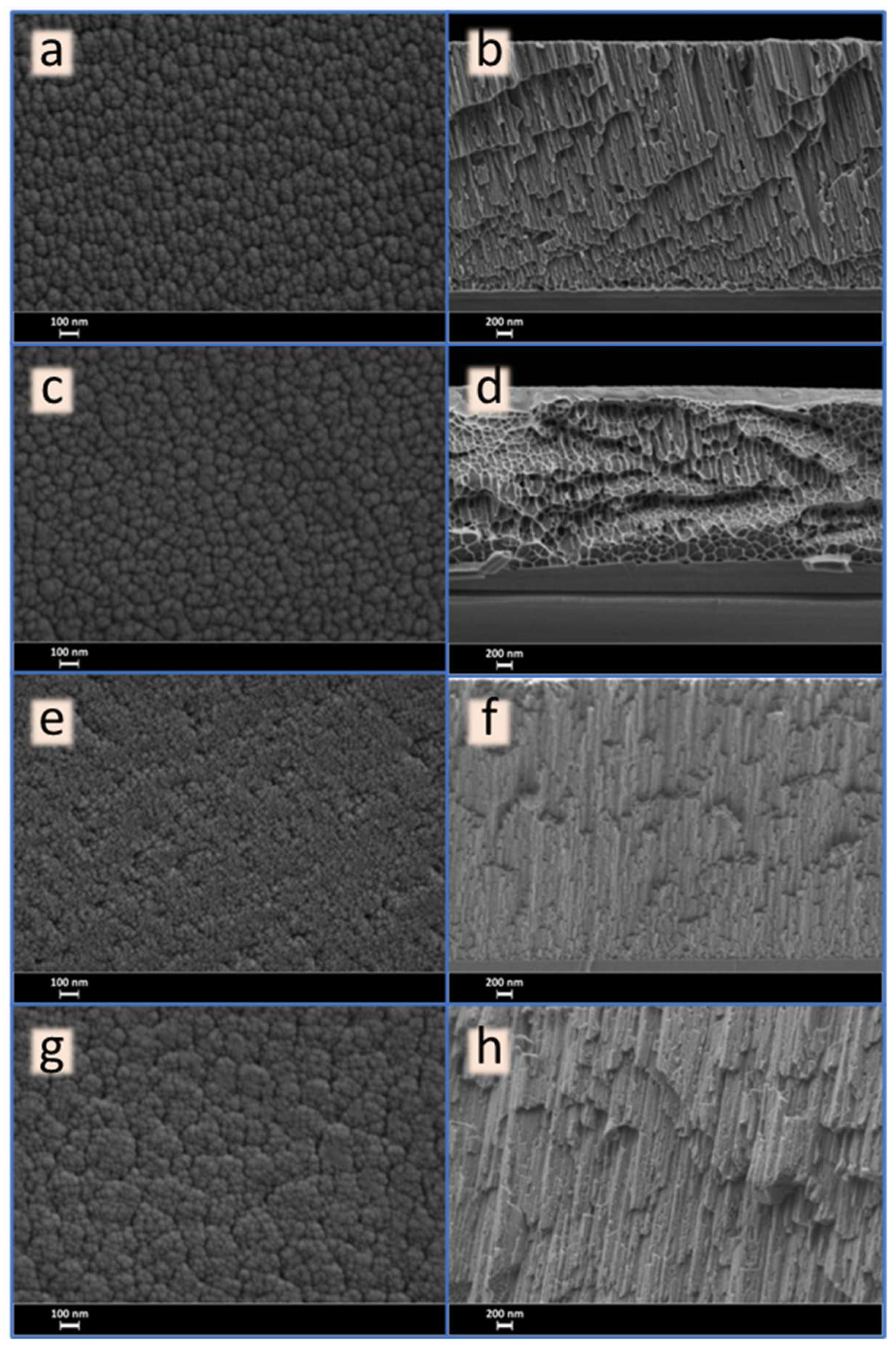
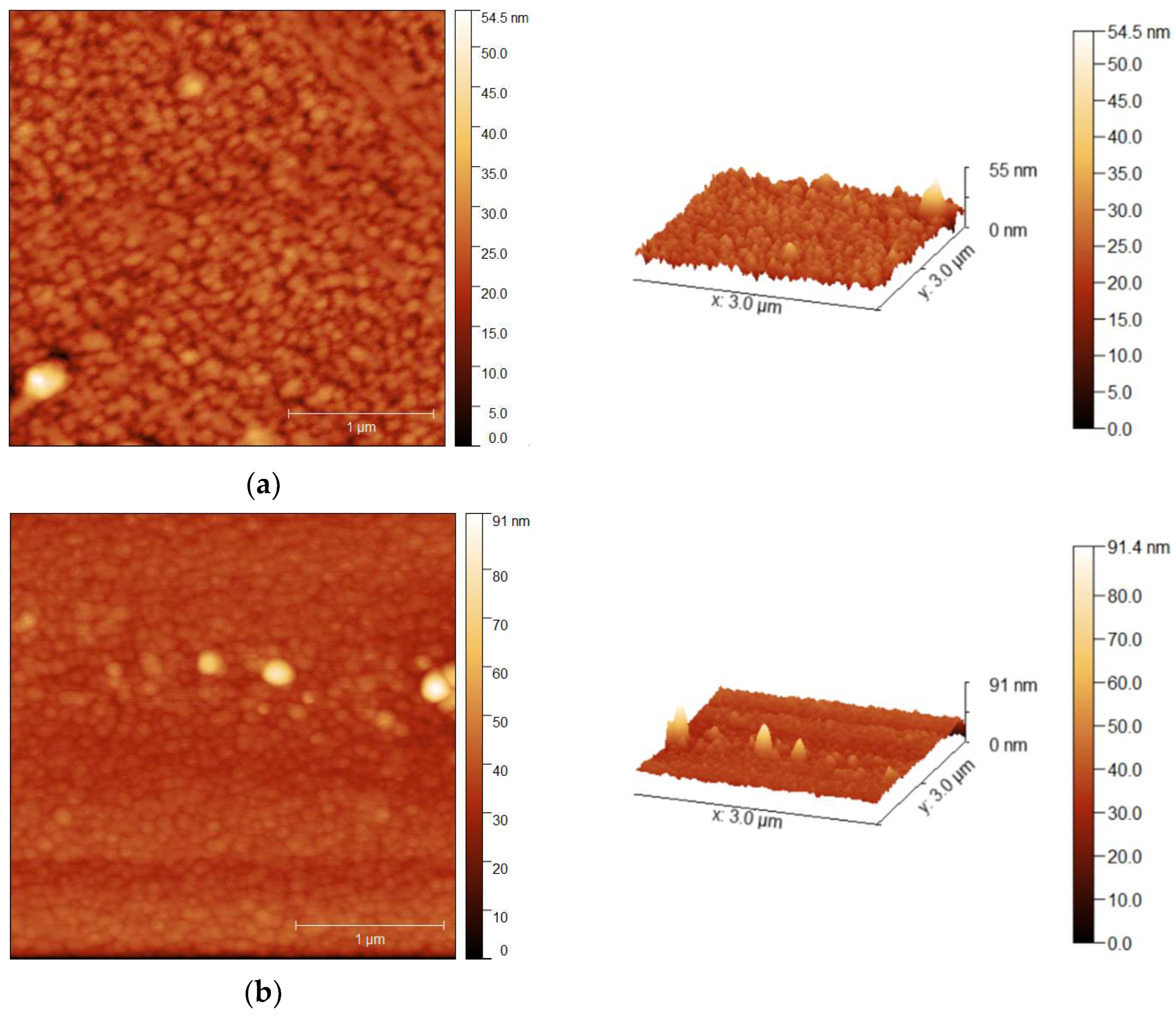
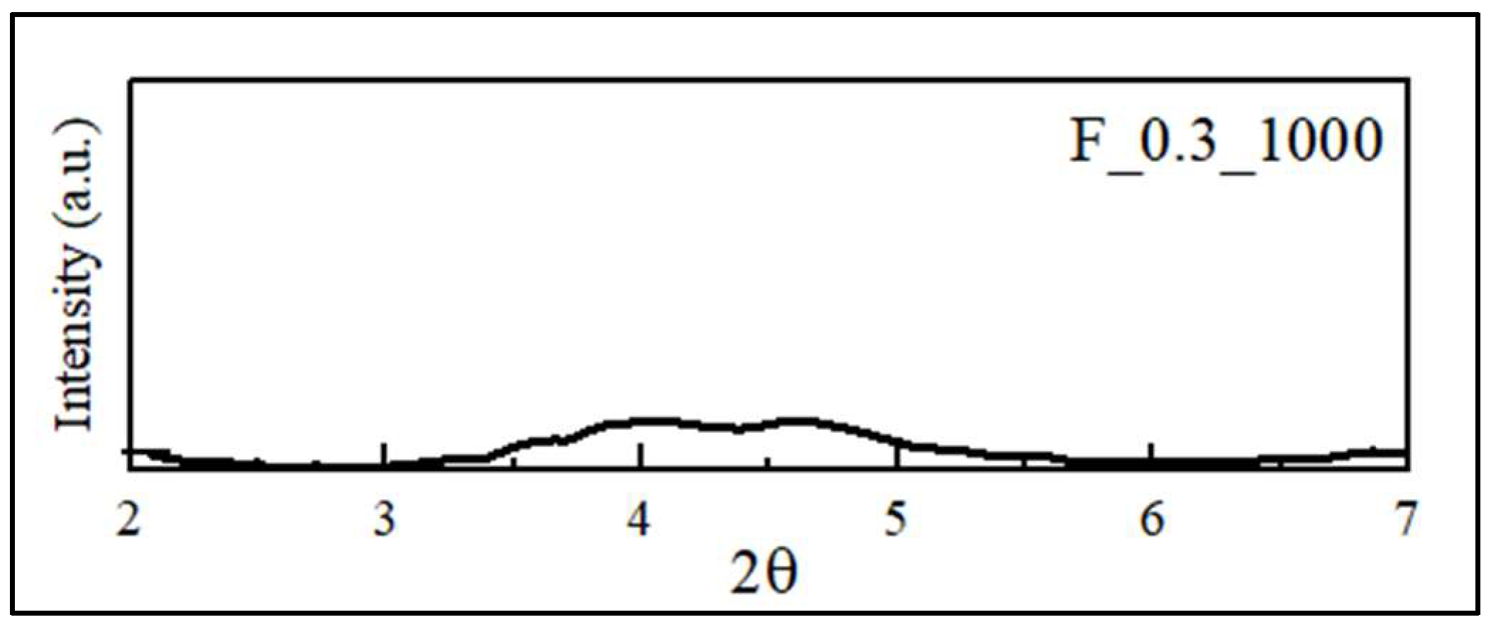
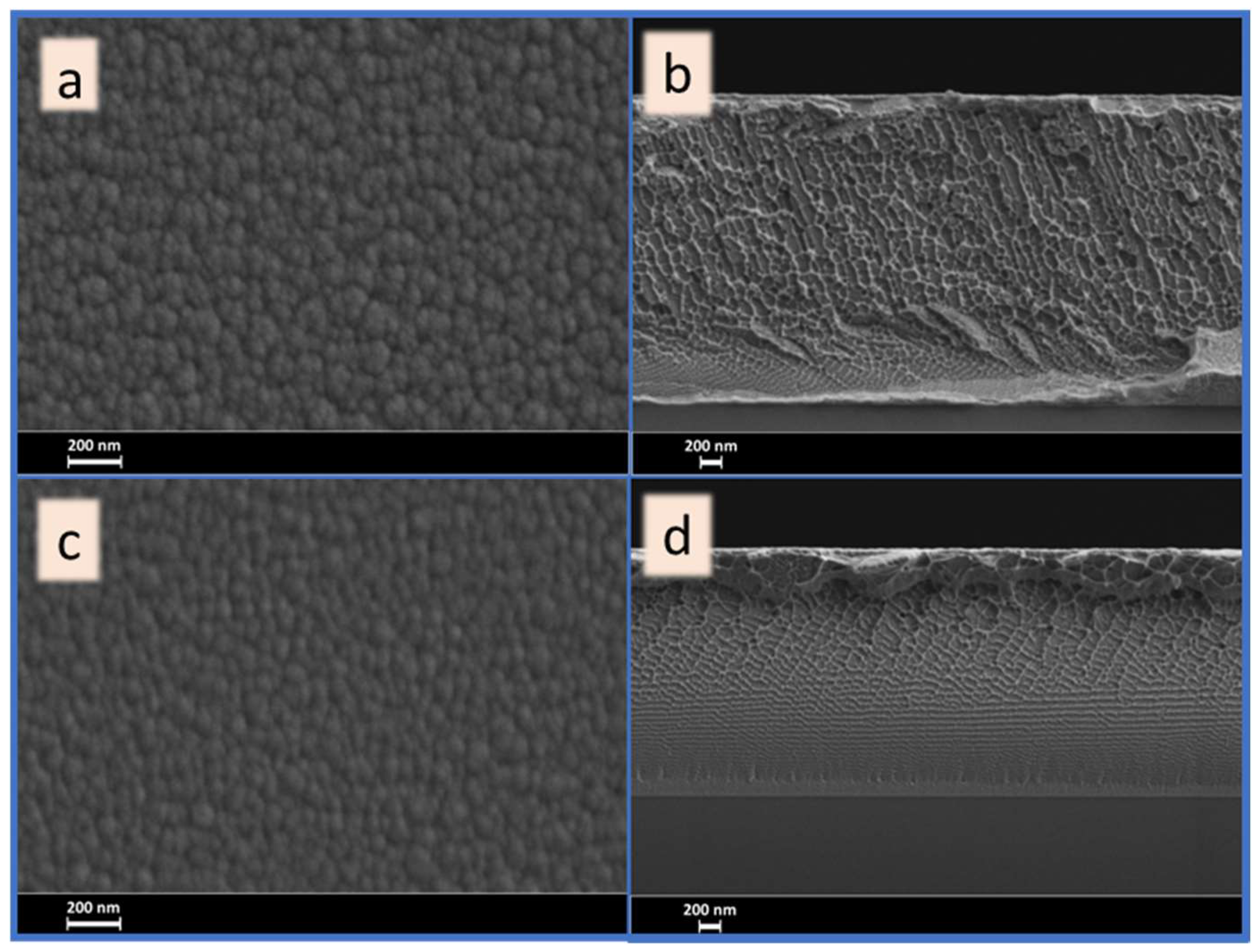
3.1. As-Deposited Films

Table 2 shows the chemical composition of the films obtained through EDS. All the films present minor amounts of oxygen (below 4.0 at.%), and this content is similar for all the films under study. Therefore, to have a more precise idea of the films’ stoichiometry, EDS results are presented after quantifying only titanium and nickel. The Ni and Ti contents presented in Table 2 correspond to the average of the four areas analyzed for each film.
As can be observed, the films are enriched in nickel, with Ni atomic percentages above 60%, a percentage much higher than that of the target from which they were prepared. This result is in accordance with the available literature and is attributed to the lower sputtering yield of Ti compared with Ni [7,20]. In fact, to obtain equiatomic chemical compositions, it is common to use a Ti-rich NiTi target [6,21], two separate targets (NiTi and Ti) [20], or even a NiTi target with Ti foils/slices superimposed [12,22]. Since the Ni-rich chemical composition is required to reach the objective of obtaining superelastic NiTi films, in this work, an equiatomic target was used to intentionally obtain films with high Ni content.
Compared with the reference film (F_0.3_1000), the increase in the power applied to the NiTi target led to a minor increase in the Ni content, while the increase in the argon pressure resulted in a slightly lower Ni%. At the beginning of the sputtering process, more nickel atoms are ejected from the target, but as the target’s surface becomes depleted in Ni, more titanium atoms are ejected, and in some cases, a steady state where the films’ chemical composition is close to the target’s chemical composition can be reached. In this study, the steady state was not reached, although the film deposited during more time (F_0.3_1000t) had somewhat more Ti.
SEM analyses were performed to characterize both the surface and cross-section morphology of the as-deposited films (Figure 1). Except for the film deposited at a higher pressure, a cauliflower shape surface morphology could be observed for all films, where the larger features should correspond to the top of the columns and, inside these features, some grains could be distinguished. The grain size of the F_0.3_1000 and F_0.3_1700 films seems similar. This cauliflower-type morphology is characteristic of metallic films deposited by magnetron sputtering, which usually results in columnar growth [23]. The SEM surface images of the F_0.3_1000 and F_0.3_1700 films, shown in Figure 1a and Figure 1c, respectively, show smaller surface features compared with the F_0.3_1000t film (Figure 1g). As a consequence of the columnar growth, the film deposited during a longer time exhibits larger features, corresponding to the top of wider columns. In the SEM image corresponding to the F_0.5_1000 film (Figure 1e), the cauliflower morphology is not noticeable, as this film has a surface morphology that seems smoother.
Regarding the cross-section morphologies, also shown in Figure 1, all the films presented rather compact morphology, without pores or discontinuities. The film deposited at the highest pressure (Figure 1f) has a dense columnar morphology, according to the Thornton [10] model, and a higher thickness than the reference film (F_0.3_1000). Higher pressure means more Ar+ ions bombarding the target(s) surface and more collisions of the ejected atoms when traveling towards the substrates. In the present case, the first effect prevailed, and an increase in thickness was observed for the film deposited using a higher pressure. The increase in thickness could also indicate a less dense film.
The F_0.3_1000, F_0.3_1700, and F_0.3_1000t films’ cross-section presented an interesting morphology; in particular, the film deposited applying a higher power to the NiTi target. In the SEM cross-section image of the F_0.3_1700 film (Figure 1d), vein-like features, which are characteristic of metallic glass thin films produced by sputtering, can be observed [24,25]. The increase in the power applied to the target should be responsible for the more notorious vein-like morphology. This morphology points to a more ductile behavior and could suggest the presence of a film with a higher elastic recovery.
The influence of the deposition time can be seen when comparing films F_0.3_1000 and F_0.3_1000t under the same magnification (Figure 1b and Figure 1h, respectively). Besides the obvious higher thickness, the F_0.3_1000t film has wider columns, as expected, as time increases due to the shape of the columns.
Figure 2 shows representative AFM images of the NiTi films deposited onto Si substrates using different parameters. The films reveal rather uniform surface topographies, with grain size in the nanometer range.
The topographic images of the films are in accordance with the SEM surface micrographs, except for the film deposited at a higher pressure. The roughness values measured using AFM and resulting from an average of two different zones for each film (minimum of 4 measurements per film) are compiled in Table 3. The films under study present low roughness, and the power applied to the NiTi target, as well as the pressure, does not seem to influence the Sa and Sq values. Although the SEM surface image of the F_0.5_1000 film suggests a smoother surface, the AFM results do not corroborate it. As expected, the film deposited during a longer time has higher roughness compared with the other films due to the larger features observed at the surface of this film and that correspond to the top of the columns.
Analyzing the XRD diffractogram of Figure 3, the presence of a single broad peak for the reference film is evident (F_0.3_1000). This observation suggests the absence of crystalline phases, leading to the conclusion that this film is amorphous. All the other films show similar diffractograms, confirming the amorphous nature of the as-deposited films under study. This finding is in line with the available literature.

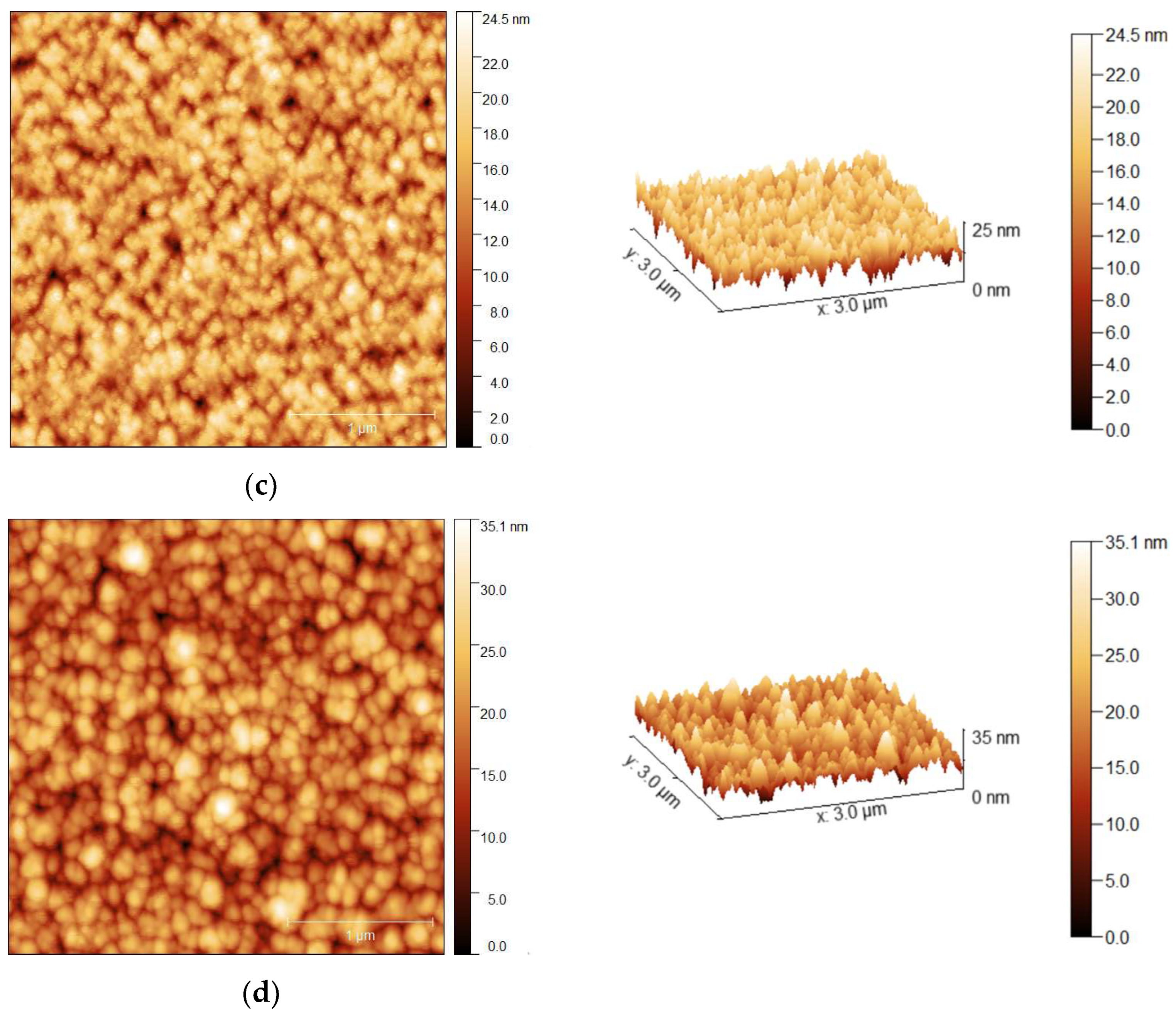
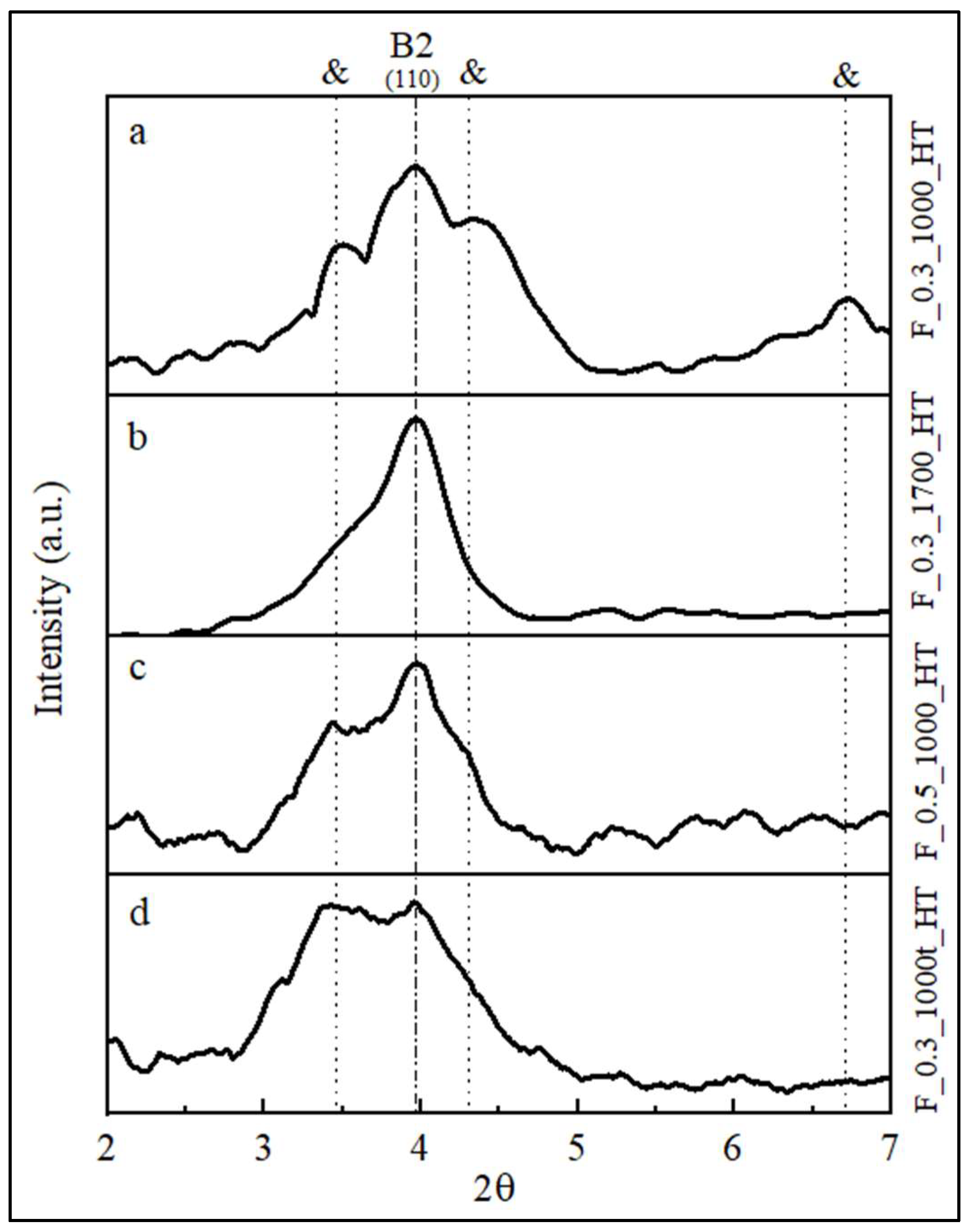
3.2. Heat-Treated Films

As described in the Materials and Methods section, the films were subjected to heat treatment at 400 °C for 1 h, being thereafter characterized. After heat treatment, the surface and cross-section of the films were analyzed by SEM. Comparing the SEM surface micrographs of Figure 4a,c with the surface SEM micrographs of the as-deposited films (Figure 1), it can be perceived that the features observed in F_0.3_1000 and F_0.3_1700 films are slightly larger, but the surface of the heat-treated films seems more compact when the voids between the columns are less defined. During heat treatment, grain growth should occur, explaining the morphological differences observed.
Cross-section SEM images of the heat-treated films are also shown in Figure 4. When analyzing the cross-section of the F_0.3_1000 and F_0.3_1700 films (Figure 4b,d), there are changes from the as-deposited to the heat-treated morphology. Although still with a vein-like appearance, the heat-treated F_0.3_1000 and F_0.3_1700 films transited to a more compact morphology, confirmed by the decrease in thickness from 3.2 to 2.9 μm and from 2.7 to 2.3 μm, respectively. A thin layer of oxide seems to have formed at the surface of both films.
After heat treatment, SR-XRD analyses were conducted to ensure that the films had crystalized, forming intermetallic phases, in particular, the desired B2 phase (austenitic phase). SR-XRD was used to study the structural characteristics of the NiTi films because it is a powerful technique that uses high-energy X-rays in transmission mode with a small beam size. SR-XRD allows for detailed structural analysis of the films, which is fundamental for materials such as NiTi that may display minor phases with reduced dimensions (precipitates) [26]. Since all the films are enriched in nickel, besides the B2 phase, the indexation of Ni-rich crystalline phases is possible. Films that were initially amorphous (Figure 3) were found to crystallize, revealing numerous XRD peaks, as can be observed in the diffractograms of Figure 5. Among these, several were indexed as B2, while a few can be identified as Ni-rich precipitates [27,28,29].
The information from the XRD diffractograms is valuable because it proves that the chosen heat-treatment temperature (400 °C) is enough to obtain the B2 phase, the main driving factor for the existence of a superelastic NiTi film. The austenite formed presents the (110) crystallographic plane for all the films. Furthermore, along with the austenite phase, the heat-treatment temperature promoted the formation of Ni-rich precipitates (highlighted by & in Figure 5), which can be interesting for improving the mechanical properties of the films, as shown in the mechanical behavior section [30].

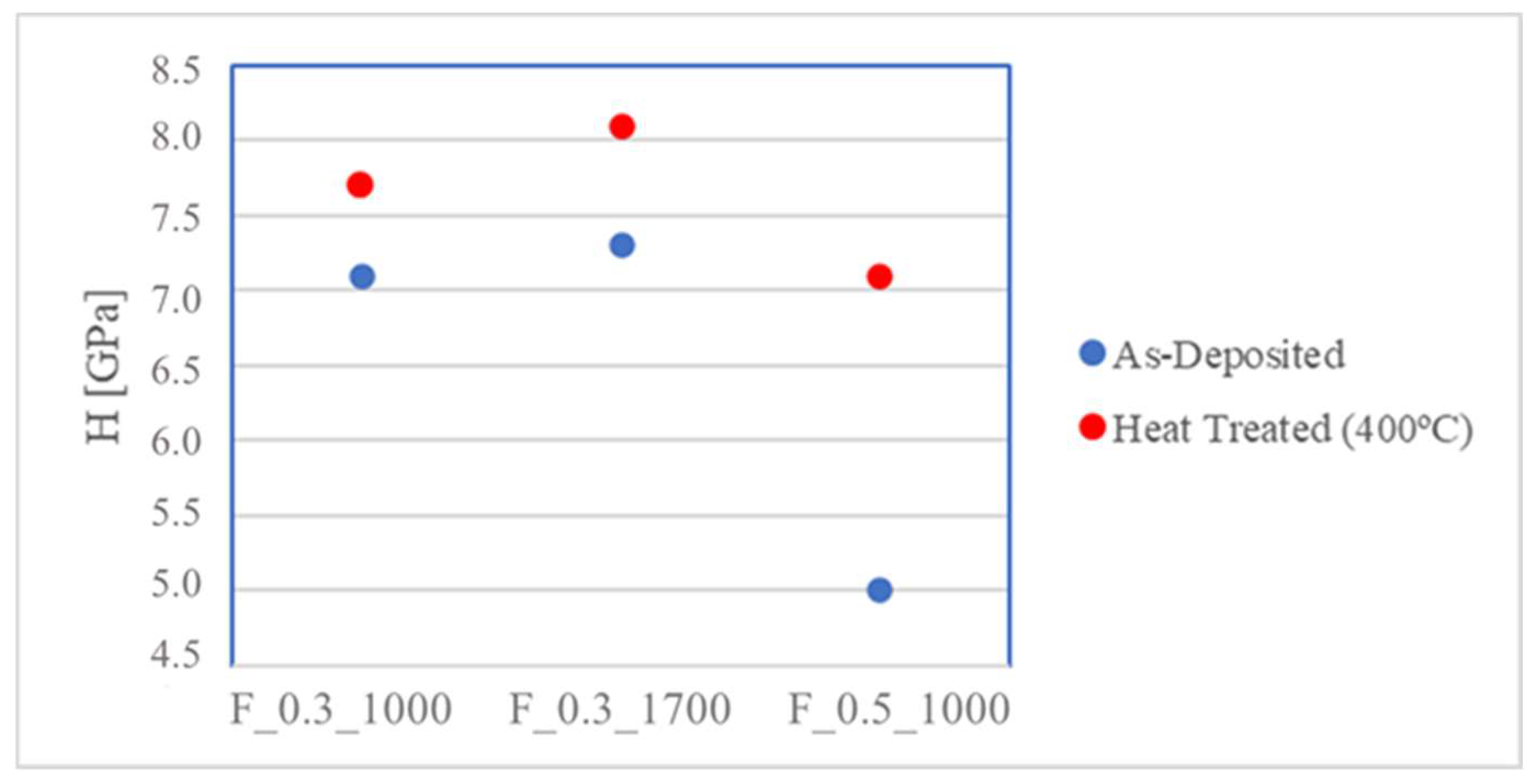
3.3. Mechanical Behavior

Table 4 shows the results of the nanoindentation experiments for the as-deposited films. In this table, the films’ thickness is also included to more easily confirm that there is no influence of the substrate on the measured hardness. Actually, as can be seen in Table 4, the maximum indentation depths are always below 10% of the films’ thickness, assuring that there is no influence of the substrate on the hardness values.
For the F_0.3_1000 and F_0.3_1700 films, a hardness of around 7 GPa and Young’s modulus close to 140 GPa was obtained, meaning that the power applied to the NiTi target does not significantly influence the films’ mechanical behavior. Indeed, these films have a similar nickel content (EDS results) and similar morphology based on the SEM surface and cross-section analyses (Figure 1a–d). For the F_0.5_1000 film, a lower hardness was obtained (5.0 GPa). The increase of the pressure also results in a decrease in the Young’s modulus. This film presents a significantly different morphology (Figure 1e,f) from the other films and that is unusual for sputtered metallic films, but based on the SEM images of Figure 1, it is difficult to infer whether the increase in the deposition pressure promotes less dense films. However, due to the interelectrode collisions, at higher pressures, the adatoms arrive at the substrate with lower mobility, and the films tend to be less dense, which can explain the lower hardness and Young’s modulus of the F_0.5_1000 film. The thickness of the F_0.5_1000 film is higher than the thickness of the F_0.3_1000 film, which is also in accordance with a less dense film for a higher deposition pressure. Compared with the film prepared using higher pressure, the elastic recovery parameter (ERP) of the other films is higher, with ERP values close to 0.21. This result is in accordance with the as-deposited films’ cross-section morphology that points to a more ductile behavior of the F_0.3_1000 and F_0.3_1700 films (see Figure 1). The ERP, defined as the ratio of recoverable indentation depth to maximum indentation depth, is a dimensionless parameter that highlights the elastoplastic behavior of the material; as ERP increases, the elastic work increases, while as it decreases, the plastic work increases [31].
Heat treating the films promoted changes in their mechanical properties, as demonstrated in Table 5. When analyzing the nanoindentation results after heat treatment at 400 °C, it is evident that the hardness and Young’s modulus increased for all films. The hardness increase is due to the formation of hard intermetallic phases but also because heat treatment promotes compaction of the films, as confirmed by SEM. In fact, the comparison between both surface and cross-section images of the films (Figure 1 and Figure 4) reveals more compact morphology after heat treatment.
In order to highlight the differences in hardness, Figure 6 shows the hardness of the as-deposited and heat-treated films. The more pronounced rise in hardness upon heat treatment is observed for the high-pressure film. After heat treatment, the F_0.3_1000_HT and F_0.3_1700_HT films still have similar hardness values, again in accordance with their similar morphology (Figure 4), while the F_0.5_1000_HT film as a slightly lower hardness. The high-pressure film has a slightly lower Ni content, and thus, the presence of Ni-rich precipitates might be slightly less pronounced, which can explain the lower hardness of this film.
Regarding Young’s modulus, there are no significant differences, and all the heat-treated films have values higher than those found in the literature for equiatomic B2-NiTi films (~95–100 GPa [11,32]). The current films are proven to have formed B2-NiTi as the major phase, which should have brought Young’s modulus closer to the literature values. The higher Young’s modulus values are probably related to the nanoindentation measurements and can be explained by the influence of the silicon substrate. Even though the maximum depths are lower than 10% of the films’ thickness, when it comes to Young’ modulus, the substrate’s influence is still possible. Tests conducted using the same nanoindentation equipment, also with a maximum load of 5 mN, revealed a reduced Young’s modulus for monocrystalline silicon around 175 GPa. Therefore, if there is an influence of the substrate, it should result in a higher Young’s modulus than expected for NiTi. It should also be noted that the measured hardness values are also higher than those expected for superelastic NiTi films. According to the work of Ni et al. [32], the hardness of a superelastic NiTi film deposited onto an aluminum alloy substrate is 4.7 GPa, and Young’s modulus is 95 GPa. These mechanical properties were obtained by nanoindentation using loads ranging from 5 to 200 mN. Interestingly, the H/Er ratio reported by Ni et al. [32] (~0.050) is similar to the H/Er values of the heat-treated films under study, which are between 0.051 and 0.054. Comparing Table 4 and Table 5, it is possible to conclude that the heat-treated films always have higher ERP than the corresponding as-deposited film, indicating an increase in the elastic work, which is consistent with a superelastic behavior and thus, together with the presence of austenite phase, suggests that the Ni-rich films under study are superelastic.

4. Conclusions

Ni-rich films were produced by magnetron sputtering from a NiTi target using different deposition parameters. The films had to be heat-treated to obtain the NiTi shape memory alloy. The characterization of the as-deposited and heat-treated films allowed for the following conclusions to be taken:
(i) The increase in the power applied to the NiTi target results in films with a slightly higher Ni content, while the increase in pressure had the opposite effect.
(ii) The as-deposited films present a cauliflower-like surface morphology (except for the film deposited at a higher pressure), while the cross-section morphology of most films is columnar with traces of vein-like features.
(iii) The power applied to the NiTi target and the pressure do not seem to influence the roughness, with all the films presenting Sa and Sq values below 4 and 5 nm, respectively.
(iv) After deposition, all the films are amorphous, as is usual in NiTi sputtered films without substrate heating.
(v) Heat treatment is responsible for grain growth, thickness reduction, and more compact films. The vein-like cross-section morphology is dominant in the F_0.3_1000_HT and F_0.3_1700_HT films.
(vi) The 400 °C heat treatment temperature is enough to promote the crystallization of the films with the formation of austenitic B2-NiTi as a major phase together with Ni-rich precipitates.
(vii) Due to the formation of intermetallic phases, the heat treatment results in an increase in hardness in the films. Heat treatment also increases the Young’s modulus of the films. The H/Er ratio of the heat-treated films is similar to that found in the literature on superelastic NiTi films.
(viii) The elastic recovery of the Ni-rich austenitic films is higher in comparison with the corresponding as-deposited amorphous films.
Considering the conclusions above and the versatility of the sputtering technique, the high Ni content NiTi films produced show potential for MEMS applications.

Author Contributions

Conceptualization, P.F.R. and A.S.R.; methodology, A.V.F., D.S., P.F.R. and A.S.R.; formal analysis, P.F.R. and A.S.R.; investigation, A.V.F., P.F.R. and A.S.R.; writing—original draft preparation, A.V.F.; writing—review and editing, D.S., P.F.R. and A.S.R.; supervision, P.F.R. and A.S.R. All authors have read and agreed to the published version of the manuscript.

Funding

This research was funded by national funds through FCT—Fundação para a Ciência e a Tecnologia, under projects UIDB/EMS/00285/2020 and LA/P/0112/2020.

Institutional Review Board Statement

Not applicable.

Informed Consent Statement

Not applicable.

Data Availability Statement

Data are contained within the article.

Acknowledgments

We acknowledge DESY (Hamburg, Germany), a member of the Helmholtz Association HGF, for the provision of the experimental facilities. Parts of this research were carried out at PETRA III, and we would like to thank Norbert Schell and Emad Maawad for their assistance in using Hereon—X-ray Diffraction/Small Angle X-ray Scattering (EH1). Beamtime was allocated for proposal I-20221253 EC.

Conflicts of Interest

The authors declare no conflicts of interest.

References

  1. Khanlari, K.; Ramezani, M.; Kelly, P. 60NiTi: A Review of Recent Research Findings, Potential for Structural and Mechanical Applications, and Areas of Continued Investigations. Trans. Indian Inst. Met. 2018, 71, 781–799. [Google Scholar] [CrossRef]
  2. Xu, G.X.; Zheng, L.J.; Zhang, F.X.; Zhang, H. Influence of solution heat treatment on the microstructural evolution and mechanical behavior of 60NiTi. J. Alloys Compd. 2019, 775, 698–706. [Google Scholar] [CrossRef]
  3. Zhang, F.; Zheng, L.; Wang, F.; Zhang, H. Effects of Nb additions on the precipitate morphology and hardening behavior of Ni-rich Ni55Ti45 alloys. J. Alloys Compd. 2018, 735, 2453–2461. [Google Scholar] [CrossRef]
  4. Khanlari, K.; Shi, Q.; Li, K.; Hu, K.; Tan, C.; Zhang, W.; Cao, P.; Achouri, I.E.; Liu, X. Fabrication of Ni-Rich 58NiTi and 60NiTi from Elementally Blended Ni and Ti Powders by a Laser Powder Bed Fusion Technique: Their Printing, Homogenization and Densification. Int. J. Mol. Sci. 2022, 23, 9495. [Google Scholar] [CrossRef] [PubMed]
  5. Li, Y.; Dai, J.; Song, Y. Research Progress of First Principles Studies on Oxidation Behaviors of Ti-Al Alloys and Alloying Influence. Metals 2021, 11, 985. [Google Scholar] [CrossRef]
  6. Tillmann, W.; Momeni, S. In-situ annealing of NiTi thin films at different temperatures. Sens. Actuators A Phys. 2015, 221, 9–14. [Google Scholar] [CrossRef]
  7. Sharma, S.K.; Mohan, S. Influence of annealing on structural, morphological, compositional and surface properties of magnetron sputtered nickel–titanium thin films. Appl. Surf. Sci. 2013, 282, 492–498. [Google Scholar] [CrossRef]
  8. Otsuka, K.; Ren, X. Physical metallurgy of Ti–Ni-based shape memory alloys. Prog. Mater. Sci. 2005, 50, 511–678. [Google Scholar] [CrossRef]
  9. Young, M.L.; Wagner, M.-X.; Frenzel, J.; Schmahl, W.W.; Eggeler, G. Phase volume fractions and strain measurements in an ultrafine-grained NiTi shape-memory alloy during tensile loading. Acta Mater. 2010, 58, 2344–2354. [Google Scholar] [CrossRef]
  10. Thornton, J.A. The microstructure of sputter-deposited coatings. J. Vac. Sci. Technol. A Vac. Surf. Film. 1986, 4, 3059–3065. [Google Scholar] [CrossRef]
  11. Tillmann, W.; Momeni, S. Deposition of superelastic composite NiTi based films. Vacuum 2014, 104, 41–46. [Google Scholar] [CrossRef]
  12. Bai, X.; Cai, Q.; Xie, W.; Zeng, Y.; Chu, C.; Zhang, X. In-situ crystalline TiNi thin films deposited by HiPIMS at a low substrate temperature. Surf. Coat. Technol. 2023, 455, 129196. [Google Scholar] [CrossRef]
  13. Kumar, A.; Singh, D.; Kaur, D. Grain size effect on structural, electrical and mechanical properties of NiTi thin films deposited by magnetron co-sputtering. Surf. Coat. Technol. 2009, 203, 1596–1603. [Google Scholar] [CrossRef]
  14. Fu, Y.; Huang, W.; Du, H.; Huang, X.; Tan, J.; Gao, X. 26 Characterisation of TiNi Shape-Memory Alloy Thin Films for MEMS Applications. Surf. Coat. Technol. 2001, 145, 107–112. [Google Scholar] [CrossRef]
  15. Marupalli, B.C.G.; Behera, A.; Aich, S. A Critical Review on Nickel–Titanium Thin-Film Shape Memory Alloy Fabricated by Magnetron Sputtering and Influence of Process Parameters. Trans. Indian Inst. Met. 2021, 74, 2521–2540. [Google Scholar] [CrossRef]
  16. Oliver, W.C.; Pharr, G.M. Measurement of hardness and elastic modulus by instrumented indentation: Advances in understanding and refinements to methodology. J. Mater. Res. 2004, 19, 3–20. [Google Scholar] [CrossRef]
  17. Logothetidis, S.; Charitidis, C. Elastic properties of hydrogen-free amorphous carbon thin films and their relation with carbon–carbon bonding. Thin Solid Films 1999, 353, 208–213. [Google Scholar] [CrossRef]
  18. Fasaki, I.; Koutoulaki, A.; Kompitsas, M.; Charitidis, C. Structural, electrical and mechanical properties of NiO thin films grown by pulsed laser deposition. Appl. Surf. Sci. 2010, 257, 429–433. [Google Scholar] [CrossRef]
  19. Hammersley, A.P.; Svensson, S.O.; Hanfland, M.; Fitch, A.N.; Hausermann, D. Two-dimensional detector software: From real detector to idealised image or two-theta scan. High Press. Res. 1996, 14, 235–248. [Google Scholar] [CrossRef]
  20. Shih, C.-L.; Lai, B.-K.; Kahn, H.; Phillips, S.M.; Heuer, A.H. A robust co-sputtering fabrication procedure for TiNi shape memory alloys for MEMS. J. Microelectromech. Syst. 2001, 10, 69–79. [Google Scholar] [CrossRef]
  21. Tillmann, W.; Momeni, S. Comparison of NiTi thin films sputtered from separate elemental targets and Ti-rich alloy targets. J. Mater. Process. Technol. 2015, 220, 184–190. [Google Scholar] [CrossRef]
  22. Miyazaki, S.; Ishida, A. Martensitic transformation and shape memory behavior in sputter-deposited TiNi-base thin films. Mater. Sci. Eng. A 1999, 273–275, 106–133. [Google Scholar] [CrossRef]
  23. Gachon, J.-C.; Rogachev, A.; Grigoryan, H.; Illarionova, E.; Kuntz, J.-J.; Kovalev, D.; Nosyrev, A.; Sachkova, N.; Tsygankov, P. On the mechanism of heterogeneous reaction and phase formation in Ti/Al multilayer nanofilms. Acta Mater. 2005, 53, 1225–1231. [Google Scholar] [CrossRef]
  24. Apreutesei, M.; Steyer, P.; Billard, A.; Joly-Pottuz, L.; Esnouf, C. Zr–Cu thin film metallic glasses: An assessment of the thermal stability and phases’ transformation mechanisms. J. Alloys Compd. 2015, 619, 284–292. [Google Scholar] [CrossRef]
  25. Chang, J.-C.; Lee, J.-W.; Lou, B.-S.; Li, C.-L.; Chu, J.P. Effects of tungsten contents on the microstructure, mechanical and anticorrosion properties of Zr–W–Ti thin film metallic glasses. Thin Solid Films 2015, 584, 253–256. [Google Scholar] [CrossRef]
  26. Rodrigues, P.F.; Fernandes, F.B.; Magalhães, R.; Camacho, E.; Lopes, A.; Paula, A.; Basu, R.; Schell, N. Thermo-mechanical characterization of NiTi orthodontic archwires with graded actuating forces. J. Mech. Behav. Biomed. Mater. 2020, 107, 103747. [Google Scholar] [CrossRef]
  27. Hou, H.; Hamilton, R.F.; Horn, M.W. Crystallization of nanoscale NiTi alloy thin films using rapid thermal annealing. J. Vac. Sci. Technol. B Nanotechnol. Microelectron. Mater. Process. Meas. Phenom. 2016, 34, 06KK01. [Google Scholar] [CrossRef]
  28. Somsen, C.; Zähres, H.; Kästner, J.; Wassermann, E.; Kakeshita, T.; Saburi, T. Influence of thermal annealing on the martensitic transitions in Ni–Ti shape memory alloys. Mater. Sci. Eng. A 1999, 273–275, 310–314. [Google Scholar] [CrossRef]
  29. Otsuka, K.; Wayman, C.M. Mechanism of Shape Memory Effect and Superelasticity. In Shape Memory Materials, 1st ed.; Cambridge University Press: New York, NY, USA, 1998; ISBN 0-521-44487-X. [Google Scholar]
  30. Yu, H.; Qiu, Y.; Young, M.L. Influence of Ni4Ti3 precipitate on pseudoelasticity of austenitic NiTi shape memory alloys deformed at high strain rate. Mater. Sci. Eng. A 2021, 804, 140753. [Google Scholar] [CrossRef]
  31. Di Egidio, G. Evaluation by nanoindentation of the influence of heat treatments and the consequent induced microstructure on the mechanical response of the heat-treated L-PBF AlSi10Mg alloy. Metall. Ital. 2022, 6, 8–16. [Google Scholar]
  32. Ni, W.; Cheng, Y.-T.; Lukitsch, M.; Weiner, A.M.; Lev, L.C.; Grummon, D.S. Novel layered tribological coatings using a superelastic NiTi interlayer. Wear 2005, 259, 842–848. [Google Scholar] [CrossRef]
Figure 1. SEM surface micrographs of as-deposited films: (a) F_0.3_1000, (c) F_0.3_1700, (e) F_0.5_1000, and (g) F_0.3_1000t. SEM cross-section micrographs of as-deposited films: (b) F_0.3_1000, (d) F_0.3_1700, (f) F_0.5_1000, and (h) F_0.3_1000t.
Coatings 14 00138 g001
Figure 2. 2D and 3D AFM images (3 μm × 3 μm) of as-deposited films: (a) F_0.3_1000, (b) F_0.3_1700, (c) F_0.5_1000, and (d) F_0.3_1000t.
Coatings 14 00138 g002aCoatings 14 00138 g002b
Figure 3. Synchrotron radiation XRD diffractograms—F_0.3_1000.
Coatings 14 00138 g003
Figure 4. SEM surface micrographs of heat-treated films: (a) F_0.3_1000_HT and (c) F_0.3_1700_HT; SEM cross-section micrographs of heat-treated films: (b) F_0.3_1000_HT and (d) F_0.3_1700_HT.
Coatings 14 00138 g004
Figure 5. Synchrotron radiation XRD diffractograms: (a) F_0.3_1000_HT, (b) F_0.3_1700_HT, (c) F_0.5_1000_HT, and (d) F_0.3_1000t_HT.
Coatings 14 00138 g005
Figure 6. Hardness of as-deposited and heat-treated films.
Coatings 14 00138 g006
Table 1. Deposition parameters of the NiTi films produced using magnetron sputtering.
FilmTargetPressure
[Pa]
Power Density
[Wmm−2]
Dep Time
[min]
Thickness
[μm]
F_0.3_1000NiTi0.34.44 × 10−2
(1000 W)
603.2
F_0.3_1700NiTi0.37.56 × 10−2
(1700 W)
282.7
F_0.5_1000NiTi0.54.44 × 10−2
(1000 W)
603.4
F_0.3_1000tNiTi0.34.44 × 10−2
(1000 W)
1205.1
Table 2. Chemical composition of the NiTi films.
FilmNi
[at.%]
Ti
[at.%]
F_0.3_100060.7 ± 0.439.3 ± 0.4
F_0.3_170061.4 ± 0.138.6 ± 0.1
F_0.5_100060.3 ± 0.339.7 ± 0.3
F_0.3_1000t59.4 ± 0.440.6 ± 0.4
Table 3. Sa and Sq values of the NiTi films measured using AFM.
FilmF_0.3_1000F_0.3_1700F_0.5_1000F_0.3_1000t
Sa (nm)2.5 ± 0.12.6 ± 0.42.6 ± 0.13.8 ± 0.4
Sq (nm)3.4 ± 0.14.0 ± 0.83.4 ± 0.34.9 ± 0.6
Table 4. Mechanical properties of the as-deposited films.
FilmThickness
[μm]
Max Depth
[nm]
Plastic Depth
[nm]
Hardness
[GPa]
Er
[GPa]
E
[GPa]
ERP
F_0.3_10003.2162.1 ± 5.8133.9 ± 6.27.1 ± 0.5137 ± 8143 ± 80.211 ± 0.02
F_0.3_17002.7159.8 ± 6.3131.6 ± 6.77.3 ± 0.6138 ± 5145 ± 50.215 ± 0.02
F_0.5_10003.4193.9 ± 9.4166.1 ± 9.95.0 ± 0.5116 ± 7119 ± 70.168 ± 0.02
Er—reduced Young’s modulus; E—Youngs modulus; ERP—Elastic recovery parameter.
Table 5. Mechanical properties of the heat-treated films.
FilmMax Depth
[nm]
Plastic Depth
[nm]
Hardness
[GPa]
Er
[GPa]
E
[GPa]
ERP
F_0.3_1000_HT154.8 ± 6.9126.7 ± 6,87.7 ± 0.7143 ± 9151 ± 90.222 ± 0.02
F_0.3_1700_HT150.6 ± 4.6122.6 ± 5.08.1 ± 0.6147 ± 6156 ± 60.229 ± 0.02
F_0.5_1000_HT160.6 ± 5.1133.0 ± 5.87.1 ± 0.5140 ± 5147 ± 50.208 ± 0.02
Disclaimer/Publisher’s Note: The statements, opinions and data contained in all publications are solely those of the individual author(s) and contributor(s) and not of MDPI and/or the editor(s). MDPI and/or the editor(s) disclaim responsibility for any injury to people or property resulting from any ideas, methods, instructions or products referred to in the content.

