Article

Enhanced Stability of Solution-Processed Indium–Zinc–Tin–Oxide Transistors by Tantalum Cation Doping

1
School of Materials Science and Engineering, Shanghai University, Shanghai 200072, China
2
Key Laboratory of Advanced Display and System Application, Ministry of Education, Shanghai University, Shanghai 200072, China
3
School of Mechatronics and Automation, Shanghai University, Shanghai 200072, China
4
School of Microelectronics, Shanghai University, Shanghai 200072, China
5
Huzhou Key Laboratory of Medical and Environmental Applications Technologies, School of Life Sciences, Huzhou University, Huzhou 313000, China
*
Authors to whom correspondence should be addressed.
Coatings 2023, 13(4), 767; https://doi.org/10.3390/coatings13040767
Submission received: 17 March 2023 / Revised: 3 April 2023 / Accepted: 11 April 2023 / Published: 13 April 2023
(This article belongs to the Special Issue Advanced Films and Coatings Based on Atomic Layer Deposition)

Abstract

:
Highly stable metal oxide thin film transistors (TFTs) are required in high-resolution displays and sensors. Here, we adopt a tantalum cation (Ta5+) doping method to improve the stability of zinc–tin–oxide (ZnSnO) TFTs. The results show that Ta5+-doped TaZnSnO TFT with 1 mol% concentration exhibits excellent stability. Compared with the undoped device, the oxygen vacancy defects of TaZnSnO thin films reduce from 38.05% to 18.70%, and the threshold voltage shift (ΔVth) reduces from 2.36 to 0.71 V under positive bias stress. We attribute the improved stability to the effective suppression of the oxygen vacancy defects, which is confirmed by the XPS results. In addition, we also prepared TaInZnSnO TFT devices with 1 mol% Ta5+ doping concentration. Compared with the 1 mol% Ta5+-doped TaZnSnO TFTs, the μ increases two-fold from 0.12 to 0.24 cm2/Vs, and the Vth decreases from 2.29 to 0.76 V in 1 mol% Ta5+-doped TaInZnSnO TFT with an In:Zn:Sn ratio of 4:4:3, while the device remains highly stable with a ΔVth of only 0.90 V. The injection of Ta5+ provides a novel strategy for the enhancement of the stability in ZnSnO-based TFTs.

1. Introduction

Amorphous oxide semiconductor (AOS) thin film transistors (TFTs) are widely applied due to their higher mobility and better large-area uniformity than amorphous silicon TFTs. For example, they are used in displays, CMOS image sensors, and touch sensors [1,2]. Today, AOS TFTs can be fabricated by vacuum deposition processes such as magnetron sputtering, atomic layer deposition (ALD), and chemical vapor deposition. However, the high fabrication cost of these vacuum deposition processes limits their large-scale application. As a newly developed AOS fabrication method, solution processing techniques offer the possibility of depositing thin films in a simple printing or coating manner, enabling the fabrication of low-cost and high-performance electrical devices [3,4,5], and the chemical composition of AOS films is easy to control compared to other physical deposition methods [6,7,8].
Solution-processed zinc–tin–oxide (ZnSnO) TFTs were widely investigated due to their excellent properties, such as a low-temperature synthesis process, simple fabrication, low cost, and resource sustainable ability [9,10,11]. However, oxygen vacancies have some negative effects on oxide films. The situation of oxygen vacancy is complicated because the vacancies are in several charge states. For both binary and complex oxides, in contrast to alkali halides, oxygen vacancy in ionic oxides can have two charge states: the one-electron F+ center and the two-electron F center. The absorption bands of the F+ and F centers in most oxides occur at different energies. In addition, the diffusion characteristics of vacancies depend on their charge state [12]. Owing to the oxygen vacancy defects, it is difficult to control the mobility, threshold voltage, stability, etc., in ZnSnO TFTs [13]. It is known that these problems can be solved by doping appropriate cations as suppressors of oxygen vacancy. The principle is to control the oxygen vacancy-related trap states by introducing an element that has higher binding energy with oxygen [14]. In recent years, several doping elements, including Zr [6], Ba [2], P [15], and Sb [16], have been reported to improve the stability of devices by suppressing oxygen vacancy. Unfortunately, they both have large threshold voltages (Vth) (~5−10 V) [6,16,17,18]. Therefore, one of the keys is to reduce the Vth while improving stability. Tantalum (Ta5+) has a larger oxygen bonding dissociation energy (Ta-O dissociation energy of 799.1 kJ/mol) than those of Zn (Zn-O dissociation energy of 159.4 kJ/mol) and Sn (Sn-O dissociation energy of 531.8 kJ/mol) [19], which is expected to be an effective oxygen vacancy inhibitor. However, Ta5+ doping may cause a decrease in field-effect mobility (μ) and an increase in Vth. Indium ions (In3+), possessing a special electron configuration of (n − 1) d10ns0 (n is the principal quantum number) [20], play a significant role in improving the μ of the TFTs. However, the effect of In3+ on the performance of TaZnSnO TFTs still needs to be further investigated.
Dielectric layers are also critical to TFT device performance, and high-quality dielectric layers can be prepared via ALD, which uses a binary reaction split into two self-limiting chemical reactions in a repeated alternate deposition sequence. The ALD technique has a lot of advantages, including high controllability for composition and thickness, excellent reproducibility, and low deposition temperatures [21,22]. Al2O3, with good insulating properties grown by ALD (ALD-Al2O3), is one of the most widely studied materials [23]. Until now, the solution-processed method has not been investigated to prepare films on ALD-Al2O3, due to the low hydrophilicity of the ALD-Al2O3 surface [24]. To overcome this problem, we adopted UV–ozone treatment to improve the hydrophilicity of the ALD-Al2O3 surface.
Herein, we first report the TaZnSnO and TaInZnSnO TFTs fabricated by the solution method on ALD-Al2O3. The effect of Ta5+ doping on the properties of TaZnSnO thin films and their associated application to TFTs are investigated. Ta5+ doping can improve the stability of the ZnSnO thin films and decrease carrier concentration due to the suppression of oxygen vacancies. Moreover, Ta5+ injection was also developed to explore the electrical properties and stability of their associated TaInZnSnO TFTs.

2. Experiments

The 0.3 M ZnSnO precursor was synthesized by dissolving Zn(CH3COO)2·2H2O) and SnCl2·2H2O in 2-methoxyethanol with the molar ratio of Zn:Sn = 4:3 in an airtight glove box to cut off O2 and H2O, and the water and oxygen content of the glove box in the laboratory are lower than 0.1 ppm and lower than 10.7 ppm, respectively. After the precursor solution was stirred for 15 min to fully dissolve the solute, ethanolamine was added as a stabilizer to avoid turbidity and precipitation of the precursor solution. TaCl5 was then dissolved into the ZnSnO solution to form the TaZnSnO precursor solutions with Ta5+ molar ratios of 0.5, 1, and 2 mol%. We also prepared 0.3 M TaInZnSnO precursor by dissolving In(NO3)3·xH2O into the 1 mol% Ta5+ doping concentration TaZnSnO precursor solution with the molar ratio of In:Zn:Sn = 4:4:3. Then, the prepared precursor solution was stirred in a water bath heating pot with a magnetic stirrer at 60 °C for 2 h, followed by stirring for 12 h to process homogeneous hydrolysis.
Before coating, the Al2O3 gate dielectrics of approximately 50 nm thick were formed on the heavily doped p-type single crystal semiconductor Si (100) substrates (1–10 Ω·cm) using ALD (TFS-200, Beneq, Finland) at 250 °C with trimethylaluminum and H2O, and the purge time was 10 s. Then, the hydrophilicity of the Al2O3 gate dielectrics was improved by UV–ozone treatment for 10 min to enhance the uniformity of the coating. After that, the precursor solutions were spin-coated on the Al2O3 films at 500 r/min for 5 s, followed by 2000 r/min for 30 s. Then, they were heated on a hot plate at 150 °C for 15 min. Finally, the devices were annealed at 500 °C for 1 h. Al 200-nm-thick was deposited by thermal evaporation to form the source and drain electrodes through a shadow mask; the channel width (W) and channel length (L) were 1000 and 50 μm, respectively. The schematic structure of the TFTs with various doping ratios is illustrated in Figure 1a. The prepared devices were annealed at 300 °C in the air for 15 min on the hot annealing furnace. This step is for the formation of good ohmic contact between the semiconductor and metal electrodes to reduce the resistivity. To evaluate the optical performance of thin films, ZnSnO and TaZnSnO films were grown on quartz glass substrates through the same process.
The thermal decomposition characteristics of the precursor solution were obtained by thermogravimetric analysis (TGA). The test conditions were varied from room temperature to 800 °C with a 10 °C/min heating rate in an air environment. The water contact angle test was performed by using contact angle meter (Contact Angle Meter Model SL200KS, Solon, China). The surface morphologies of the films were characterized by atomic force microscope (AFM, nanonaviSPA-400 SPM, SII Nano Technology Inc., Chiba City, Japan). Measurement of optical transmittance was performed using spectrometer (HITACHI U-3900H, Tokyo, Japan) at room temperature. The crystal structure of the thin films was characterized by X-ray diffraction (XRD, Rigaku D/max-rB, Tokyo, Japan), and the composition was analyzed by X-ray photoelectron spectroscopy (XPS, Thermo Scientific K-Alpha+, Waltham, MA, USA). Electrical characteristics were tested with a semiconductor characterization system (Keithley, 4200-SCS, Cleveland, OH, USA).

3. Results and Discussion

In order to improve the hydrophilicity of the Al2O3 film and facilitate the subsequent spin coating, we performed UV–ozone treatment on it, and used the contact angle (θ) and surface free energy (γ) to characterize the difference in the hydrophilicity of the film. The surface free energy of thin film can be calculated with the following formula [25]:
γ S = γ S d + γ S p
γ L ( 1 + cos θ ) = 2 γ S d γ L d + 2 γ S p γ L p
where γS and γL are the surface free energy of solid and liquid, and the p component and d component correspond to their polar component and dispersion component, respectively. The water contact angles of Al2O3 films before and after UV–ozone treatment are 50.737° and 10.937°, as shown in Figure 1b,c. In addition, we measured the contact angles of Al2O3 before and after UV–ozone treatment using 2-methoxyethanol, as shown in Figure 1d,e, and calculated the corresponding γS. The contact angle (17.383°) of the Al2O3 surface of 2-methoxyethanol after UV–ozone treatment is also smaller than the contact angle 50.857° of the surface before UV–ozone treatment. According to the contact angle test results of the film, the γS of the Al2O3 film after UV–ozone treatment is 89.794 mN/m, and the γS before UV–ozone treatment is 59.285 mN/m. The lower water contact angle and higher γS indicate that the film is more hydrophilic. The results show that UV–ozone treatment can significantly improve the hydrophilicity of Al2O3 films, which makes a better condition for the subsequent spin coating of the ZnSnO-based films. The leakage current characteristics of 50 nm ALD-Al2O3 dielectric are charted in Figure 1f. The Al2O3 produces a leakage current density of 10−8 A/cm2 at 2 MV/cm, which is suitable for TFT application. The surface morphologies of the Al2O3 were analyzed by AFM, as shown in Figure 1g. The Al2O3 thin film exhibits a smooth surface with a root mean squared (RMS) value of 0.33 nm. The smooth surface of the gate dielectric can suppress the surface roughness-induced leakage current and achieve expeditious carrier transport in the channel. Figure 1h–k present the surface morphologies of the TaZnSnO thin films with different Ta5+ doping concentrations. The RMS values are 2.43, 1.11, 1.30, and 0.66 nm for TaZnSnO thin films with Ta5+ doping concentrations of 0, 0.5, 1, and 2 mol%, respectively. The RMS roughness of the films decreases slightly with the increase in doping concentration. Rough surface morphology of the undoped ZnSnO thin films is associated with the growth of the columnar structure; the growth of the columnar structure in TaZnSnO films is suppressed by doped Ta element, which may result from the formation of stresses by the different ion sizes of Zn and Sn, and the segregation of Ta cations [26]. The smooth surface roughness of the active layer facilitates the adhesion ability to the source and drain electrodes.
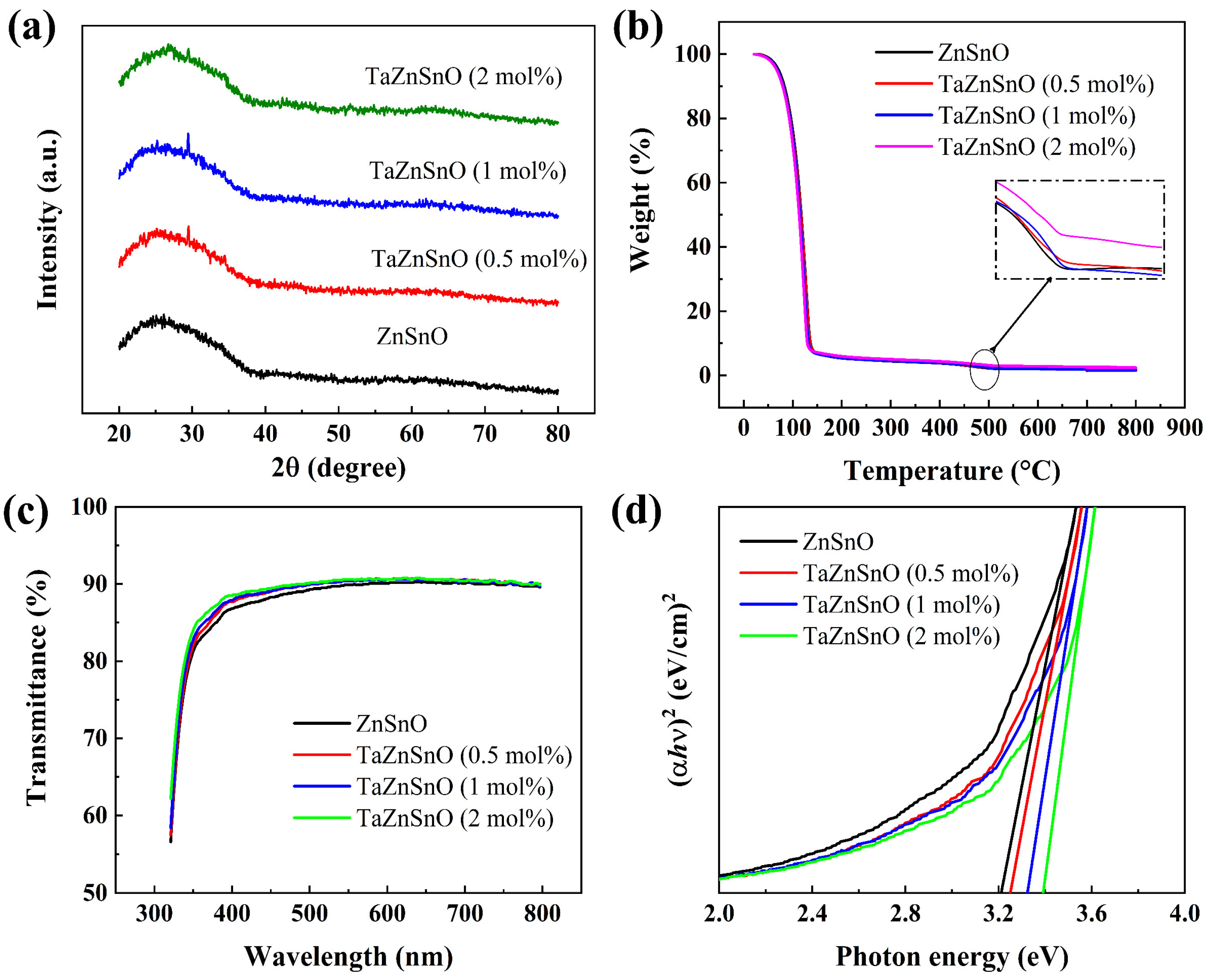
Figure 2a shows the GIXRD pattern of TaZnSnO films with different Ta5+ doping ratios. No XRD peak corresponding to TaZnSnO films is found, which indicates that the TaZnSnO films have an amorphous structure. Grain boundaries usually act as preferential paths for impurity diffusion and leakage current, resulting in an inferior dielectric performance. In comparison, an amorphous structure provides a fast transport path for carriers [27,28], which may be beneficial for the preparation of large-size oxide TFTs. As shown in Figure 2b, two apparent weight loss stages could be observed for all the solutions by TGA analyses. The initial weight loss stage happened in the range of 70–150 °C. This phenomenon was caused by the evaporation of volatile nitrates and the hydrolysis of Zn(CH3COO)2·2H2O, SnCl2·2H2O, and TaCl5. In the temperature range of 150–500 °C, only a slight loss of weight due to the conversion of the relevant hydroxides to the corresponding oxides through dehydroxylation and condensation reactions. No apparent weight loss was observed at temperatures above 500 °C, implying that the precursor solution completely formed a dense metal oxide film. Therefore, we chose 500 °C as the annealing temperature of the thin film according to the analysis results.
The optical transmittance spectra of the TaZnSnO films were analyzed to depict the effect of Ta5+ doping on the optical transmittance, as shown in Figure 2c. The optical transmittance of all samples shows about 90% transmission in the visible region. With the increase in Ta5+ content, the average transmittance of TaZnSnO films increases slightly, indicating that TaZnSnO film has great potential to be applied on transparent electronic devices. The transmittance became slightly higher by increasing Ta5+ addition, due to its wider bandgap. The optical bandgap (Eg) is related to the absorption coefficient (α) by the following equation [29]:
α h v = ( h v E g ) 1 2
where α, h, and ν are the optical absorption coefficient, Planck’s constant, and the incident photon frequency, respectively. The absorption coefficient (α) can be extracted by the following equation:
α = ( 1 d ) ln ( 1 T )
where T is the transmittance and d is the film thickness. Figure 2d shows a plot of ( α h v )2 versus photon energy. The Eg of 0, 0.5, 1, and 2 mol% Ta5+-doped ZnSnO films are 3.21, 3.25, 3.32, and 3.39 eV, respectively, which are determined from the absorption spectra by extrapolation. However, there are some defects that may have some of their energy levels in the band gap. We use the Urbach rule to fit the band gap as an “estimation” only, but not the true “calculation” [30]. A larger Eg requires the carriers to have higher energy to shift from the valence band toward the conduction band. The generation of carriers by AOS depends on the generation of oxygen vacancies according to the following equation [6]:
O O X V O .. + 2 e + 1 2 O 2
Hence, Ta5+ doping reduces the carrier concentration and reduces the defect states generated by oxygen vacancies.
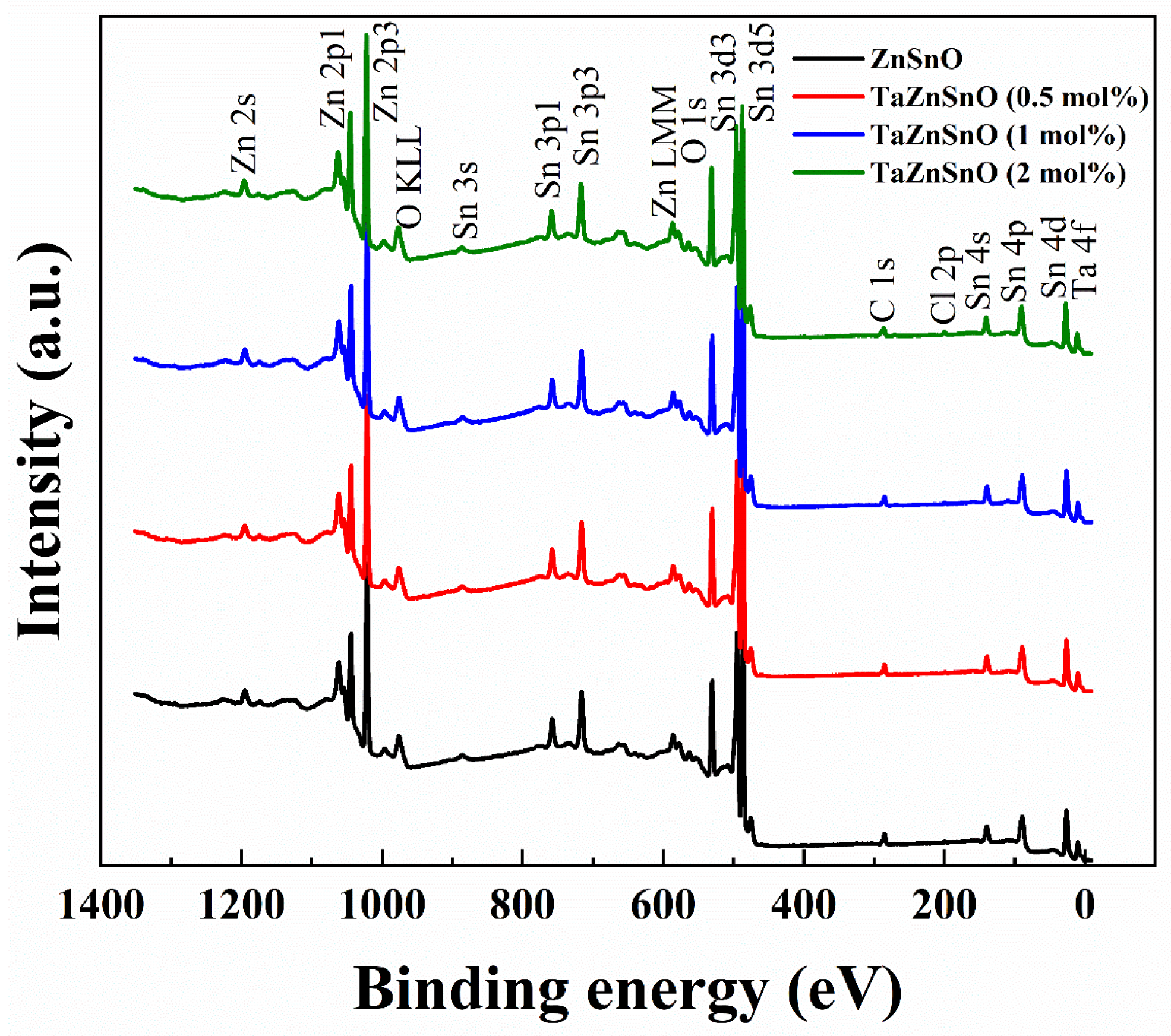
To further investigate the effect of Ta5+ doping on the chemical bonding states of TaZnSnO thin films, XPS was used to test the O1s spectra of the TaZnSnO thin films with different Ta5+ doping concentrations; Figure 3 shows the XPS survey spectra of the TaZnSnO thin films, and the XPS peaks of the major lattice components of Zn (2s, 2p1, and 2p3), Sn (3s, 3p1, 3p3, 3d3, 3d5, 4s, 4p, and 4d), Ta (4f), O (1s), C (1s), and Cl (2p) are visible. In addition, the photoelectron peaks of the main elements, Zn, O, Auger Zn LMM, and O KLL, can be seen, and it is almost consistent with previously reported data [31].
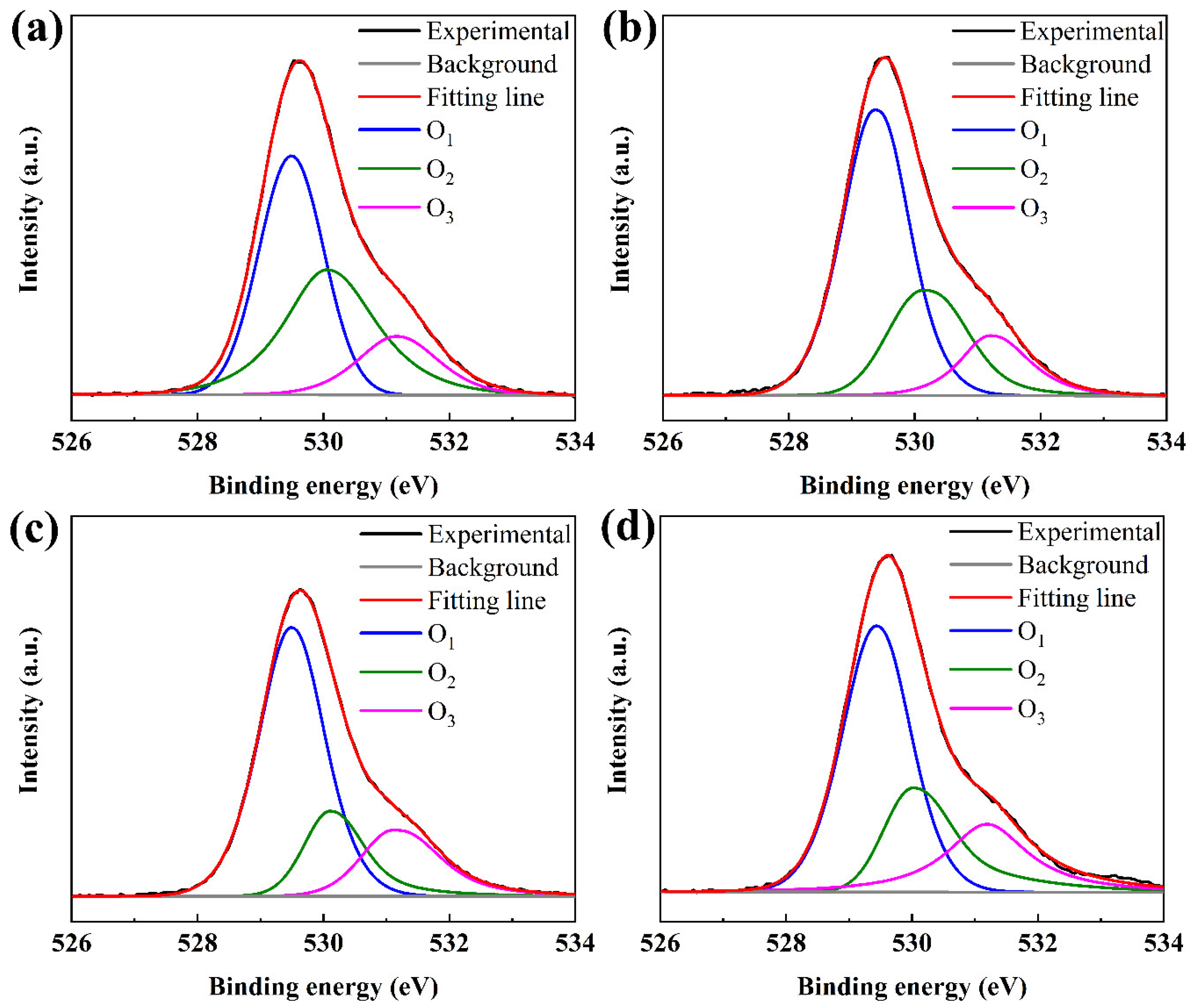
As shown in Figure 4a–d, all peaks were calibrated by taking the carbon C1s (284.5 eV). The XPS O1s spectra of the TaZnSnO films were fitted by three component peaks with the Gaussian distribution and approximate center frequency of 529.8 eV (O1), 530.5 eV (O2), and 531.6 eV (O3), respectively. The O1 is attributed to the bonding of the oxygen ion (O2−) to metal ions (M–O) such as Ta5+, Zn2+, and Sn2+ (Sn4+). The O2 is related to the oxygen-related defect states in TaZnSnO films [32]. The O3 is associated with loosely bound oxygen on the surface of films such as C, O2, O2, and H2O [33]. O2/(O1 + O2 + O3) is defined as the relative quantity of oxygen vacancy in the TaZnSnO thin films. The ratio of O2/(O1 + O2 + O3) was calculated to be 38.05%, 26.26%, 18.70%, and 24.81% for TaZnSnO films with Ta5+ doping concentrations of 0, 0.5, 1, and 2 mol%, respectively. The oxygen vacancy concentration decreased to a minimum with Ta5+ content in 1 mol% for the TaZnSnO film, due to the greater difference in electronegativity between tantalum (1.50) [34] and O (3.44) than that between Zn (1.65), Sn (1.96), and O [35]. Therefore, Ta5+ has a stronger attraction ability to oxygen ions. Moreover, the ratio of oxygen vacancy defects increased from 18.70% to 24.81%, with the doping concentration of Ta5+ increasing from 1 mol% to 2 mol%, which may be caused by over doping leading to more trap states and the result concurring with the SS (Table 1). So, we can conclude that the appropriate amount of Ta5+ doping can effectively suppress the oxygen defect concentration in the ZnSnO film.
A positive bias stress (PBS) test was carried out to further study the effects of Ta5+ doping on the stability of TaZnSnO TFTs, as shown in Figure 5a–d. The test conditions were under darkness with a stress voltage of 5 V at room temperature. The transfer curves of TaZnSnO TFTs both shifted toward the positive direction with the increase in stress time due to the electron trapping that occurred at the channel/dielectric interface. The method of extracting the electrical parameters in TFT can be found in Reference [36] and is summarized in Table 1. The value of Vth increased from 0.29 to 3.43 V, and the μ decreased from 0.38 to 0.06 cm2/Vs with the Ta5+ doping concentration increasing from 0 to 2 mol%. For oxide TFT, the μ is confirmed to be affected by both shallow traps near the conduction band and the generation of carriers from oxygen vacancies in the interface [29]. According to our results, the phenomenon of μ decreased with the increase in Ta5+ concentration, indicating that Ta5+ doping has a stronger effect on suppressing the number of electrons than making the electrons freer, which reduces the carrier concentration of ZnSnO films. In addition, with the Ta5+ doping concentration increased from 0 to 1 mol%, the value of SS decreased from 0.103 to 0.067 V/decade. The SS is closely related to the total trap density (Ntrap) [37], which can be extracted using the following equation:
N trap = [ S S log ( e ) k T / q 1 ] C i q
where Ci, T, and k are the capacitance per unit area of the insulator, the absolute temperature, and Boltzmann’s constant, respectively. It should be noted that the SS increased from 0.067 to 0.149 V/decade, with the Ta5+ doping rate continuing to increase to 2 mol%, which can be attributed to the generation of more trap states due to the higher doping concentration of Ta5+.
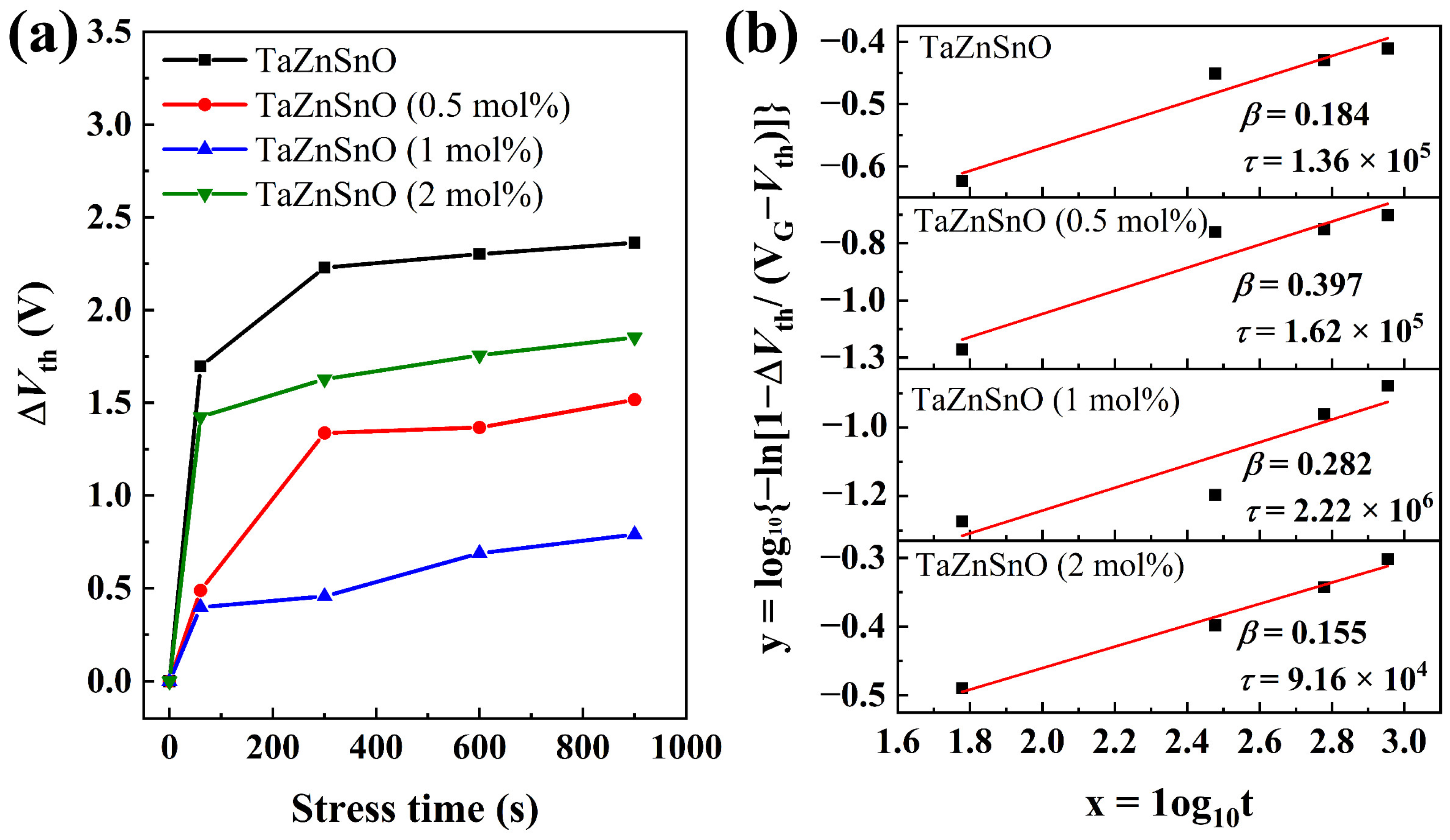
Figure 6a demonstrates the threshold voltage shifts (ΔVth) of the transfer curves for the various TaZnSnO TFTs under the different PBS times. The undoped ZnSnO TFT shows a relatively large ΔVth of 2.36 V. Compared with the ZnSnO TFT, the TaZnSnO TFTs show relatively small ΔVth of 1.74, 0.71, and 1.57 V, and Ta5+ doping concentrations of 0.5, 1, and 2 mol%, respectively. The results demonstrate that the PBS stability of TFTs was improved significantly with proper Ta5+ content, as oxygen vacancies are suppressed by Ta5+ doping. The time dependence of ΔVth can be described by the stretching exponential equation [29]:
Δ V th = ( V G V th ) { 1 exp [ ( t τ ) β ] }
where τ is the characteristics of carrier trapping time, and β is the stretched-exponential exponent. The actual stress voltage applied to the device would be lower for higher Ta5+-doped TFTs due to the increase in Vth. However, the characteristics of carrier trapping time τ and the stretched-exponential exponent β hardly depend on the bias stress amplitude. According to the above formulas, the values of τ and β extracted from the equation are 1.36 × 10⁵, 1.62 × 10⁵, 2.22 × 10⁶, and 9.16 × 10⁴ s, and 0.184, 0.397, 0.282, and 0.155 for the TaZnSnO TFTs with Ta5+ doping of 0, 0.5, 1, and 2 mol%, respectively. The fitted curve described by Equation (7) is shown in Figure 6b. The τ is related to the potential barrier for the trapping layer, and an oxide TFT device with a high τ value demonstrates better stability because τ is related to the potential barrier for trapping as τ = τ0 exp (Eτ/kT) (where Eτ and τ0 are the average effective energy barrier and thermal prefactor for emission over the barrier, respectively). Accordingly, it is concluded that the 1 mol% Ta5+-doped TaZnSnO TFT shows better stability due to lower trap density.
Although the TaZnSnO TFTs with 1 mol% Ta5+ doping exhibited excellent stability, the electrical properties of TaZnSnO TFTs need to be further improved. Thus, the Ta5+ doping method with the In:Zn:Sn ratio of 4:4:3 was carried out in Figure 7a. Compared with the TaZnSnO TFTs, the μ of TaInZnSnO TFT increases from 0.12 to 0.24 cm2/Vs. The TaInZnSnO TFT shows a ΔVth of 0.90 V, as shown in Figure 7b. In addition, the Vth decreased from 2.29 to 0.76 V, the Ion/Ioff ratio increased from 105 to 106, and the SS increased from 0.067 to 0.167 V/decade, indicating the larger trapping at the channel-insulator interface, which leads to deterioration of the stability. The obtained τ and β are 6.50 × 10⁶ s and 0.23 for the TaInZnSnO TFT, respectively. Therefore, we conclude that a TaInZnSnO TFT with better stability and electrical performance can be obtained by doping Ta5+ in an appropriate proportion.

4. Conclusions

In summary, we first reported TaZnSnO TFTs fabricated by the solution method on ALD-Al2O3 films. The effects of different Ta5+ doping concentrations on the microstructure were investigated, as well as the surface morphology and oxygen vacancy defect characteristics of the films. The results indicate that UV–ozone treatment can significantly improve the hydrophilicity of Al2O3 films, which makes a better condition for the subsequent spin coating of the ZnSnO-based films. All of the films are amorphous, the RMS roughness of the films decreases slightly, and the optical transmittance of all samples shows about 90% transmission in the visible region. TaZnSnO TFTs with 1 mol% Ta5+ doping have excellent stability relative to ZnSnO TFT, and its ΔVth reduced from 2.36 to 0.71 V since the oxygen vacancy defects decreased from 38.05% to 18.70%. Additionally, Ta5+-doped TaInZnSnO TFT with an In:Zn:Sn ratio of 4:3:3 was also developed to explore the electrical properties and stability of their associated TaInZnSnO TFTs. The results show that the Vth of the TaInZnSnO TFT is relatively lower by a factor of three, and μ is twice as high as that of the TaZnSnO TFT while maintaining stability, with a ΔVth of only 0.90 V. Consequently, such TaInZnSnO TFTs with highly stable and low Vth characteristics can be applied in the field of high-resolution displays and sensors.

Author Contributions

Conceptualization: X.D.; data curation, X.D.; formal analysis, H.X., P.L., Z.C. and B.Y.; funding acquisition, X.D.; investigation, B.W. and C.F.; methodology, H.X., B.W. and C.F.; project administration, X.D. and J.Z.; resources, X.D.; software, H.X., P.L., Z.C., B.Y. and C.F.; supervision, X.D. and J.Z.; validation, P.L., B.W., C.F. and X.D.; writing—original draft, H.X. and X.D.; writing—review and editing, H.X. and X.D. All authors have read and agreed to the published version of the manuscript.

Funding

This work is supported by the National Natural Science Foundation of China (62274105), and C. Fu acknowledges the support of the National Natural Science Foundation of China (21902063).

Institutional Review Board Statement

Not applicable.

Informed Consent Statement

Not applicable.

Data Availability Statement

Not applicable.

Conflicts of Interest

The authors declare no conflict of interest.

References

  1. Kim, J.; Park, J.; Yoon, G.; Khushabu, A.; Kim, J.-S.; Pae, S.; Cho, E.-C.; Yi, J. Effect of IGZO thin films fabricated by Pulsed-DC and RF sputtering on TFT characteristics. Mater. Sci. Semicond. Process. 2020, 120, 105264. [Google Scholar] [CrossRef]
  2. Kim, C.-H.; Park, Y.J.; Seo, J.H.; Kim, H.-K. Highly stable Ba-addition InZnSnO channels of light emitting transistors and thin film transistors. J. Alloys Compd. 2022, 900, 163472. [Google Scholar] [CrossRef]
  3. Liu, A.; Liu, G.; Zhu, H.; Shin, B.; Fortunato, E.; Martins, R.; Shan, F. Eco-friendly, solution-processed In-W-O thin films and their applications in low-voltage, high-performance transistors. J. Mater. Chem. C 2016, 4, 4478–4484. [Google Scholar] [CrossRef]
  4. Kim, Y.J.; Oh, S.; Yang, B.S.; Han, S.J.; Lee, H.W.; Kim, H.J.; Jeong, J.K.; Hwang, C.S.; Kim, H.J. Impact of the Cation Composition on the Electrical Performance of Solution-Processed Zinc Tin Oxide Thin-Film Transistors. ACS Appl. Mater. Interfaces 2014, 6, 14026–14036. [Google Scholar] [CrossRef] [PubMed]
  5. Kim, S.H.; Yoon, J.; Yun, S.O.; Hwang, Y.; Jang, H.S.; Ko, H.C. Ultrathin Sticker-Type ZnO Thin Film Transistors Formed by Transfer Printing via Topological Confinement of Water-Soluble Sacrificial Polymer in Dimple Structure. Adv. Funct. Mater. 2013, 23, 1375–1382. [Google Scholar] [CrossRef]
  6. Choi, W.S.; Jo, H.; Kwon, M.S.; Jung, B.J. Control of electrical properties and gate bias stress stability in solution-processed a-IZO TFTs by Zr doping. Curr. Appl. Phys. 2014, 14, 1831–1836. [Google Scholar] [CrossRef]
  7. Hashemi, A.; Bahari, A. Synthesis and characterization of silanized-SiO2/povidone nanocomposite as a gate insulator: The influence of Si semiconductor film type on the interface traps by deconvolution of Si2s. Curr. Appl. Phys. 2018, 18, 1546–1552. [Google Scholar] [CrossRef]
  8. Hashemi, A.; Bahari, A.; Ghasemi, S. Synthesis and Characterization of Cross-Linked Nanocomposite as a Gate Dielectric for p-Type Silicon Field-Effect Transistor. J. Electron. Mater. 2018, 47, 3717–3726. [Google Scholar] [CrossRef]
  9. Sanctis, S.; Koslowski, N.; Hoffmann, R.; Guhl, C.; Erdem, E.; Weber, S.; Schneider, J.J. Toward an Understanding of Thin-Film Transistor Performance in Solution-Processed Amorphous Zinc Tin Oxide (ZTO) Thin Films. ACS Appl. Mater. Interfaces 2017, 9, 21328–21337. [Google Scholar] [CrossRef]
  10. Wang, Z.; Jeon, S.-H.; Hwang, Y.-J.; Lee, S.-H.; Jang, J.; Kang, I.M.; Kim, D.-K.; Bae, J.-H. Physico-Chemical Origins of Electrical Characteristics and Instabilities in Solution-Processed ZnSnO Thin-Film Transistors. Coatings 2022, 12, 1534. [Google Scholar] [CrossRef]
  11. Hu, S.; Xu, M.; Peng, C.; Chen, L.; Liu, H.; Li, X. Solution-processed high stability top-gate W and F co-doped ZnSnO thin film transistors. Appl. Phys. Lett. 2023, 122, 123502. [Google Scholar] [CrossRef]
  12. Popov, A.I.; Kotomin, E.A.; Maier, J. Basic properties of the F-type centers in halides, oxides and perovskites. Nucl. Instrum. Methods Phys. Res. Sect. B Beam Interact. Mater. At. 2010, 268, 3084–3089. [Google Scholar] [CrossRef]
  13. Dai, S.; Wang, T.; Li, R.; Wang, Q.; Ma, Y.; Tian, L.; Su, J.; Wang, Y.; Zhou, D.; Zhang, X.; et al. Preparation and electrical properties of N-doped ZnSnO thin film transistors. J. Alloys Compd. 2018, 745, 256–261. [Google Scholar] [CrossRef]
  14. Lee, B.H.; Park, J.; Kumar, A.; Choi, S.; Kim, D.H.; Lee, S.Y. Structural and electronic properties with respect to Si doping in oxygen rich ZnSnO amorphous oxide semiconductor. Mater. Today Commun. 2022, 33, 104809. [Google Scholar] [CrossRef]
  15. Yang, H.; Yang, W.; Su, J.; Zhang, X. Enhancement-mode thin film transistor using amorphous phosphorus-doped Indium–Zinc–Tin-Oxide channel layer. Mater. Sci. Semicond. Process. 2022, 137, 106228. [Google Scholar] [CrossRef]
  16. Baek, J.H.; Seol, H.; Cho, K.; Yang, H.; Jeong, J.K. Comparative Study of Antimony Doping Effects on the Performance of Solution-Processed ZIO and ZTO Field-Effect Transistors. ACS Appl. Mater. Interfaces 2017, 9, 10904–10913. [Google Scholar] [CrossRef]
  17. Huang, C.-X.; Li, J.; Fu, Y.-Z.; Zhang, J.-H.; Jiang, X.-Y.; Zhang, Z.-L.; Yang, Q.-H. Characterization of dual-target co-sputtered novel Hf-doped ZnSnO semiconductors and the enhanced stability of its associated thin film transistors. J. Alloys Compd. 2016, 681, 81–87. [Google Scholar] [CrossRef]
  18. Sun, X.; Zhang, M.; Song, K.; Wei, L.; Yin, Y.; Zhang, X. Simultaneous enhancement of electrical performance and stability of zinc-tin-oxide thin-film transistors by tantalum doping. Thin Solid Film. 2020, 709, 138135. [Google Scholar] [CrossRef]
  19. Parthiban, S.; Kwon, J.-Y. Role of dopants as a carrier suppressor and strong oxygen binder in amorphous indium-oxide-based field effect transistor. J. Mater. Res. 2014, 29, 1585–1596. [Google Scholar] [CrossRef] [Green Version]
  20. Dai, S.; Wang, T.; Li, R.; Zhou, D.; Peng, Y.; Wang, H.; Zhang, X.; Wang, Y. Preparation and effects of post-annealing temperature on the electrical characteristics of Li–N co-doped ZnSnO thin film transistors. Ceram. Int. 2017, 43, 4926–4929. [Google Scholar] [CrossRef]
  21. Park, S.-H.K.; Hwang, C.-S.; Jeong, H.Y.; Chu, H.Y.; Cho, K.I. Transparent ZnO-TFT Arrays Fabricated by Atomic Layer Deposition. Electrochem. Solid-State Lett. 2008, 11, H10. [Google Scholar] [CrossRef]
  22. Li, Y.; Li, H.; Xiong, Q.; Wu, X.; Zhou, J.; Wu, J.; Wu, X.; Qin, W. Multipurpose surface functionalization on AZ31 magnesium alloys by atomic layer deposition: Tailoring the corrosion resistance and electrical performance. Nanoscale 2017, 9, 8591–8599. [Google Scholar] [CrossRef] [PubMed]
  23. Groner, M.D.; Fabreguette, F.H.; Elam, J.W.; George, S.M. Low-Temperature Al2O3 Atomic Layer Deposition. Chem. Mater. 2004, 16, 639–645. [Google Scholar] [CrossRef]
  24. Wang, L.-C.; Han, Y.-Y.; Yang, K.-C.; Chen, M.-J.; Lin, H.-C.; Lin, C.-K.; Hsu, Y.-T. Hydrophilic/hydrophobic surface of Al2O3 thin films grown by thermal and plasma-enhanced atomic layer deposition on plasticized polyvinyl chloride (PVC). Surf. Coat. Technol. 2016, 305, 158–164. [Google Scholar] [CrossRef]
  25. Hasebe, T.; Murakami, K.; Nagashima, S.; Yoshimoto, Y.; Ihara, A.; Otake, M.; Kasai, R.; Kasuya, S.; Kitamura, N.; Kamijo, A.; et al. Design for improved adhesion of fluorine-incorporated hydrogenated amorphous carbon on metallic stent: Three-layered structure with controlled surface free energy. Diam. Relat. Mater. 2011, 20, 902–906. [Google Scholar] [CrossRef]
  26. Abdullah, H.; Norazia, M.N.; Shaari, S.; Nuawi, M.Z.; Mohamed Dan, N.S. Low-doping Effects of Nanostructure ZnO: Sn tin films annealed at different temperature in Nitrogen ambient to be applied as an Anti-reflecting coating (ARC). Am. J. Eng. Appl. Sci. 2010, 3, 171–179. [Google Scholar] [CrossRef] [Green Version]
  27. Xu, W.; Wang, H.; Xie, F.; Chen, J.; Cao, H.; Xu, J.-B. Facile and Environmentally Friendly Solution-Processed Aluminum Oxide Dielectric for Low-Temperature, High-Performance Oxide Thin-Film Transistors. ACS Appl. Mater. Interfaces 2015, 7, 5803–5810. [Google Scholar] [CrossRef]
  28. Xu, H.; Ding, X.; Qi, J.; Yang, X.; Zhang, J. A Study on Solution-Processed Y2O3 Films Modified by Atomic Layer Deposition Al2O3 as Dielectrics in ZnO Thin Film Transistor. Coatings 2021, 11, 969. [Google Scholar] [CrossRef]
  29. Zhang, Y.; Zhang, H.; Yang, J.; Ding, X.; Zhang, J. Solution-Processed Yttrium-Doped IZTO Semiconductors for High-Stability Thin Film Transistor Applications. IEEE Trans. Electron Devices 2019, 66, 5170–5176. [Google Scholar] [CrossRef]
  30. Brik, M.G.; Srivastava, A.M.; Popov, A.I. A few common misconceptions in the interpretation of experimental spectroscopic data. Opt. Mater. 2022, 127, 112276. [Google Scholar] [CrossRef]
  31. Altaf, C.T.; Yolacan, D.; Sankir, N.D. Decoration of 3D ZnO nanoelectrodes with CuInS2 for solar water splitting. Mater. Lett. 2019, 236, 710–714. [Google Scholar] [CrossRef]
  32. Jeong, Y.; Bae, C.; Kim, D.; Song, K.; Woo, K.; Shin, H.; Cao, G.; Moon, J. Bias-Stress-Stable Solution-Processed Oxide Thin Film Transistors. ACS Appl. Mater. Interfaces 2010, 2, 611–615. [Google Scholar] [CrossRef] [PubMed]
  33. Abliz, A.; Gao, Q.; Wan, D.; Liu, X.; Xu, L.; Liu, C.; Jiang, C.; Li, X.; Chen, H.; Guo, T.; et al. Effects of Nitrogen and Hydrogen Codoping on the Electrical Performance and Reliability of InGaZnO Thin-Film Transistors. ACS Appl. Mater. Interfaces 2017, 9, 10798–10804. [Google Scholar] [CrossRef]
  34. Matar, S.F.; Campet, G.; Subramanian, M.A. Electronic properties of oxides: Chemical and theoretical approaches. Prog. Solid State Chem. 2011, 39, 70–95. [Google Scholar] [CrossRef]
  35. Bukke, R.N.; Avis, C.; Jang, J. Solution-Processed Amorphous In–Zn–Sn Oxide Thin-Film Transistor Performance Improvement by Solution-Processed Y2O3 Passivation. IEEE Electron Device Lett. 2016, 37, 433–436. [Google Scholar] [CrossRef]
  36. Yang, J.; Zhang, Y.; Qin, C.; Ding, X.; Zhang, J. Enhanced Stability in Zr-Doped ZnO TFTs with Minor Influence on Mobility by Atomic Layer Deposition. IEEE Trans. Electron Devices 2019, 66, 1760–1765. [Google Scholar] [CrossRef]
  37. Huang, X.D.; Ma, Y.; Song, J.Q.; Lai, P.T. High-Performamce Amorphous InGaZnO Thin-Film Transistor with ZrLaO Gate Dielectric Fabricated at Room Temperature. J. Disp. Technol. 2016, 12, 1522–1527. [Google Scholar] [CrossRef]
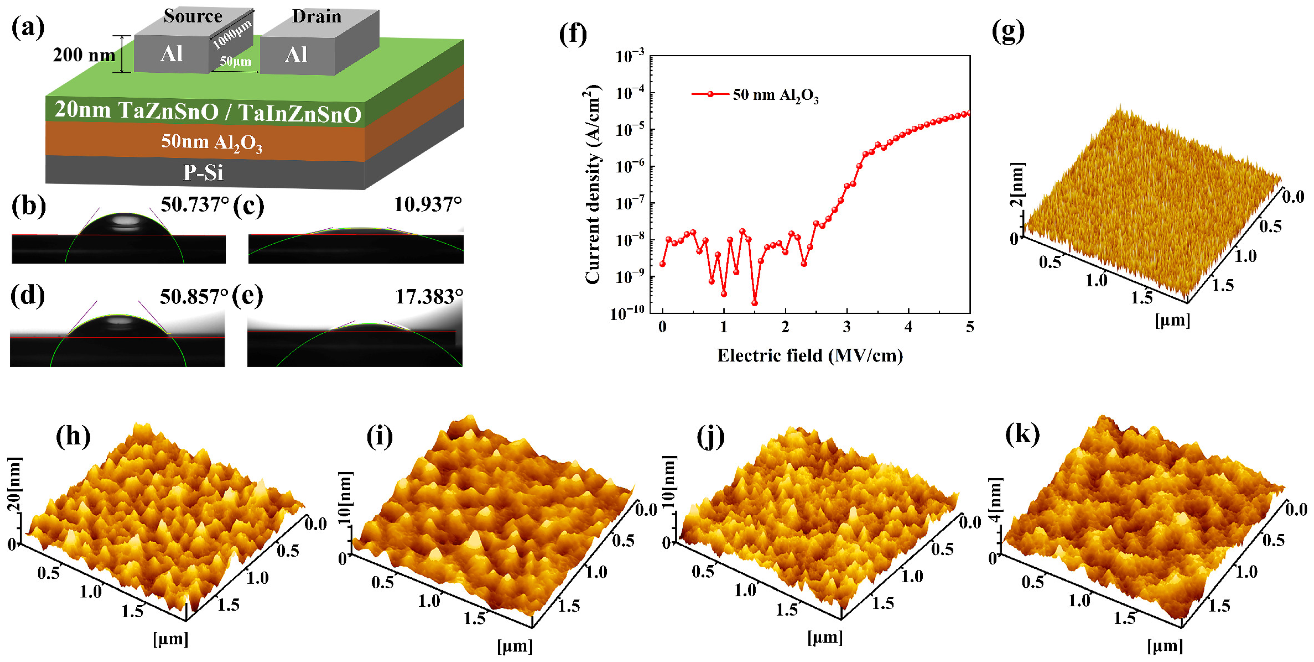
Figure 1. (a) The schematic structure of the TaZnSnO/TaInZnSnO TFTs. The water contact angles of Al2O3 films before (b) and after (c) UV–ozone treatment, and the contact angles of Al2O3 before (d) and after (e) UV–ozone treatment using 2-methoxyethanol. (f) Leakage characteristic curve of Al2O3 film. AFM images of (g) 50 nm Al2O3 dielectric layer (2 × 2 μm2) and TaZnSnO thin films with different Ta5+ doping contents (h) 0, (i) 0.5, (j) 1, and (k) 2 mol%.
Coatings 13 00767 g001
Figure 2. (a) GIXRD pattern, (b) TGA curve, (c) optical transmittance spectra, and (d) optical bandgap of TaZnSnO thin films with different Ta5+ doping concentrations.
Coatings 13 00767 g002
Figure 3. XPS survey spectra of the TaZnSnO thin films with different Ta5+ doping.
Coatings 13 00767 g003
Figure 4. XPS of O1s spectra of the TaZnSnO thin films with different Ta5+ doping levels of (a) 0, (b) 0.5, (c) 1, and (d) 2 mol%.
Coatings 13 00767 g004
Figure 5. PBS of TaZnSnO TFTs with different Ta5+ doping contents, (a) 0, (b) 0.5, (c) 1, and (d) 2 mol%.
Coatings 13 00767 g005
Figure 6. (a) The dependence of ΔVth on stress time and (b) the fitted curves described by Equation (7) for the TaZnSnO TFTs with Ta5+ doping of 0, 0.5, 1, and 2 mol%, respectively.
Coatings 13 00767 g006
Figure 7. (a) PBS of TaInZnSnO TFTs. (b) The dependence of ΔVth on stress time and the fitted curves described by Equation (7) for the TaInZnSnO TFT.
Coatings 13 00767 g007
Table 1. Electrical performance of the TaZnSnO TFTs with different Ta5+ doping concentrations.
DeviceVth (V)μ (cm2/Vs)Ion/IoffSS (V/Decade)
ZnSnO0.29 ± 0.030.38 ± 0.080~1060.103
TaZnSnO (0.5 mol%)1.26 ± 0.060.14 ± 0.005~1050.093
TaZnSnO (1 mol%)2.29 ± 0.050.12 ± 0.050~1050.067
TaZnSnO (2 mol%)3.43 ± 0.200.06 ± 0.004~1040.149
Disclaimer/Publisher’s Note: The statements, opinions and data contained in all publications are solely those of the individual author(s) and contributor(s) and not of MDPI and/or the editor(s). MDPI and/or the editor(s) disclaim responsibility for any injury to people or property resulting from any ideas, methods, instructions or products referred to in the content.