Abstract
In order to reveal the relationship between residual stress in Si layers of SiC/SiC composites and the different parameters used in their preparation, the residual stress of the coating surface was tested using X-ray sin2ψ technology and laser Raman spectroscopy. Then, the Raman shift–stress coefficient (P) and the Raman shift with free stress (ω0) were calculated as −201.41 MPa/cm−1 and 520.591 cm−1 via linear fitting with the least squares method. The results showed that all the as-sprayed Si coatings exhibited tensile stress on the surface, ranging from 53.5 to 65.9 MPa. The parameters of the spraying distance and second gas (H2) flow rate were considered to be the most important for controlling the residual stress on the coating surface. Additionally, the surface tensile stress of the Si layers could be eliminated and even changed into compressive stress by annealing above 800 °C. Furthermore, the residual stress distribution in the cross-section of the Si layers was evaluated using laser Raman spectroscopy. Additionally, the particle characteristics, such as in-flight velocity and temperature, were investigated using a diagnostic system. The results of this research contribute to increasing the understanding and control of residual stress in APS Si bond layers.
1. Introduction
New approaches are required to achieve the next breakthrough in jet engines, and those based on the use of ceramic matrix composite (CMC) materials are the most promising to reach this goal [1]. SiC/SiC composites (SiC-CMCs) are favored as advanced structural materials for use in hot compartments of gas turbine engines because of their low densities and properties with excellent high-temperature resistance [2,3,4,5].
However, SiC-CMCs have the drawback of being rapidly eroded in combustion environments, forming volatile Si(OH)4 as a result of gas streams mixing with water vapor byproducts, as indicated by Equations (1) and (2), which cause linear dimension reduction and mechanical degradation [6]. Padture et al. [7] reported a recession rate of approximately 1 μm/h for SiC-CMCs under the normal gas turbine operating conditions of commercial engines, and this significantly restricts their potential application in the field of aero engines.
Environmental barrier coatings (EBCs) have been developed to protect SiC-CMCs from water vapor degradation and thus ensure the reliability of CMC components in gas turbine operating environments [8,9,10,11,12]. In addition to water vapor stability, the key characteristics of durable EBCs are low EBC stress, EBC/substrate chemical compatibility, and adherence [13].
Generally, the coatings can be prepared using several processes, such as spark plasma sintering [14] and thermal spraying [15]. Plasma spraying has emerged as one of the potential routes to deposit thick coating layers on the structure material [16]. At present, silicon coatings prepared with atmospheric plasma spraying (APS) are the most extensively applied as bond layers of EBCs. Cracks are one of the most important forms of failure of thermal spray coatings, and this phenomenon is closely related to residual stress [17]; hence, a clear understanding of residual stress in APS Si layers is of obvious value in preventing crack failure. Generally, the stress of coatings on SiC-CMC substrates includes three parts and can be expressed as follows [13]:
where represents the thermal mismatch stress, is the aging stress, and is the growth stress. is calculated using Equation (4).
where and are the coefficients of thermal expansion (CTE) for the silicon and the SiC-CMC substrate, respectively, and represent Young’s modulus and Poisson’s ratio, respectively, of the Si coating.
represents the stress caused by changes in the Si coating’s physical, mechanical, and chemical properties during thermal exposure. Growth stress is the stress produced during the spraying process, which is close to the key plasma spraying processes, including those based on plasma power, plasma gases, etc. Generally, the thermal mismatch stress is determined by the choice of coating material. Most studies on the residual stress of EBC coatings have focused on the evolution of aging stress within a high-temperature environment [18,19]. However, the influence of this process on the residual stress in Si layers remains unclear.
Because the thickness of the APS Si layer is usually less than 100 μm, the quantification of stress in the cross-sections of the Si layers is another matter worthy of research. Laser Raman spectroscopy [20,21,22,23,24,25] is the method most commonly used for residual stress measurements of thin coatings. The stress can be calculated via Raman spectroscopy based on Equation (5) [23]:
where is the Raman shift–stress coefficient, and is the Raman shift with free stress. This equation shows that a positive Raman shift indicates compressive stress, while a negative shift indicates tensile stress.
A number of researchers have investigated residual stress from the Raman testing of Si materials and Si films [20,21,26,27,28]. A Raman shift–stress coefficient of has been reported for polysilicon [27]. However, the of Si prepared using low-pressure chemical vapor deposition (LPCVD) was found to be in [20], and it was concluded in [29] that the of porous Si film prepared using electrochemical etching rapidly decreased as porosity increased; indeed, the coefficient of 60% porosity porous silicon materials was one order of magnitude lower. In addition, the has typically been reported to be approximately , rather than constant. Therefore, the Raman shift–stress coefficient and the Raman shift with free stress of silicon may vary with the preparation process. As far as we know, the and values for APS Si coatings have not been determined until now.
In this study, Si layers on SiC-CMCs were prepared using APS technology and different parameters, with annealing at various temperatures. The residual stress was tested and calculated using an X-ray stress tester coupled with laser Raman spectroscopy to measure the residual stress in the Si layer surface and cross-section to reveal the influence of spraying and annealing parameters on residual stress. To provide supporting evidence, the microstructure and phase were also studied using SEM and XRD. By such means, we sought to characterize the residual stress of APS Si coatings and propose strategies for the greater control of this stress in the future.
2. Materials and Methods
2.1. Coating Preparation
SiC fiber-reinforced SiC composites (BIAM, Beijing, China) were used as the substrate. The silicon layer was coated on rectangular plates for the test. Before depositing the Si layer, SiC-CMC specimens were polished with SiC paper, followed by slight sandblasting with 100-mesh Al2O3 under 0.10 MPa.
Commercially available Si (99.9% purity) powder was employed. The typical morphology and phase of the Si feedstock can be seen in Figure 1, which shows that the Si particles were cubic in structure and irregularly proportioned, with particle sizes ranging from 45 to 150 μm.
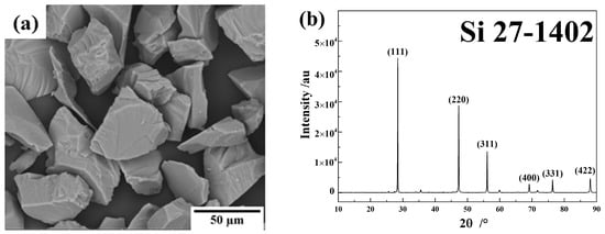
Figure 1.
Surface morphology (a) and XRD (b) of the Si powder.
Si layers were deposited on the SiC-CMC surface using the Multicoat© air plasma spraying system (Oerlikon-Metco. Co., Pfäffikon, Switzerland). The thicknesses of the Si layers were about 70~100 µm. Some sprayed Si layers were then heat-treated in a muffle furnace (DOTRUST, Beijing, China).
2.2. Inflight Particle Measurement
During the spraying process, the inflight temperatures and velocities of the Si particles in the plasma jet were monitored with an online particle diagnostic sensor (DPV-eVOLUTION, Tecnar, Saint-Bruno-de-Montarville, QC, Canada).
This system is based on a special CCD camera (Tecnar, Saint-Bruno-de-Montarville, QC, Canada) controlled by a computer and processing software and enables measuring the velocities and temperatures of inflight particles, as described in [30,31]. As the measurement volume is relatively small (<1 mm3), the data can be collected for local particles and analyzed statistically. With the automatic motion device, it can also measure the matrix data in a plane. For the matrix measurements, the gun was positioned at a fixed location, and the CCD camera was moved in the plane perpendicular to the gun axis at spray distances of 80 mm, 100 mm, and 120 mm. In this study, the 5 × 5 points measurement grid, with a step of 4 mm, was 16 × 16 mm2, and up to 5000 inflight particles were measured per point.
2.3. Analysis Methods
A PROTO LXRD X-ray diffractometer (PROTO, Taylor, MI, USA) was used to measure the stresses on the surface regions of the Si layers without considering information for the cross-section regions. The principle is widely known as the sin2ψ method, which is also based on measuring peak shifts in the XRD pattern recorded at different ψ angles [32], as indicated by Equation (6):
where is the stress constant; > 0 represents the tensile stress, while < 0 represents the compressive stress.
In this study, the target material, tube voltage, and tube current were Mn Kα, 30 kV, and 25 mA, respectively. Generally, was calculated using Equation (7); thus:
where and , respectively, represent Young’s modulus and Poisson’s ratio of the silicon, and is the Bragg angle with free stress.
In order to accurately evaluate the residual stress of the silicon layer, testing was carried out on the surfaces and polished cross-sections of the coating samples under different conditions using a Raman microscope (Horiba LabRAM HR, Tokyo, Japan) with excitation at 633 nm (HeNe Laser), and spectra with 600 grating in the range of 50 to 1000 cm−1 were collected. To avoid measurement errors caused by rising temperatures [33] and to obtain a good signal-to-noise ratio and peak intensity, the laser power was set to a level below 25% of its maximum value. Measurements were then taken at a single point 5 times at intervals of 5 s.
The microstructures of the specimens were characterized using scanning electron microscopy (FEG-SEM, Zeiss Ultra 55, Oberkochen, Germany).
The phase analysis of the coatings was achieved using X-ray diffraction (XRD, Smart Lab, Rigaku, Tokyo, Japan) at 10–90° with Cu Kα radiation (λ = 0.15406 nm). The step length and scanning rate were 0.02° and 8°/min, respectively.
3. Results and Discussion
3.1. Coating Microstructure and Phase of As-Sprayed Si Layer
In this study, coatings of nine groups were first deposited using the APS process, with the detailed parameters listed in Table 1. The current, primary gas (Ar), second gas (H2), and spraying distance were individually adjusted, with a basic parameter of P0.

Table 1.
Summary of the operating deposition parameters.
The as-sprayed Si layers exhibited similar surface morphologies, and typical SEM images prepared using P0 are shown in Figure 2. All coatings presented rough surfaces, which is characteristic of plasma-sprayed layers. Many submicronic ball-like particles were also present on the coating surface, as previously described in [34]. According to the EDS analysis results presented in Table 2, the atomic oxygen content of a typical surface area (A) was (4.96 ± 15.83)%. However, the oxygen content of a microparticle (B) was about (8.40 ± 12.82)%, increasing by a factor of more than 1.7.
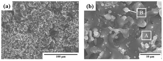
Figure 2.
(a) Typical surface image of the layer and (b) at a higher magnification (A: normal area; B: submicronic ball-like particles).
Table 2.
Oxygen content determined using EDS for the two positions (A and B) indicated in Figure 2.
In this study, the APS process was used, wherein Si powders were heated to a molten or partially molten state using plasma. The molten droplets were accelerated for impinging on the substrate at high velocities, where they solidified to form the coating [30]. Figure 3a presents a schematic diagram for Si layer deposition. The flow rate, velocity, and temperature of the inflight Si particles were statistically measured in a 16 mm × 16 mm rectangular plane (5 × 5 matrix points, with steps of 4 mm), as shown in Figure 3b–d. For the testing plane, the spraying distance was 100 mm. Other parameters are listed in Table 1. As can be seen in the flow rate contour map in Figure 3b, the Si particles were mainly distributed in an elliptically shaped area with a 45° rotation, with increased concentration close to the center. This can be explained by the form of powder feeding. The map in Figure 3c shows that the Si particles in a circle with a 5 mm radius around the center could be accelerated to a speed of 210~243 m/s.
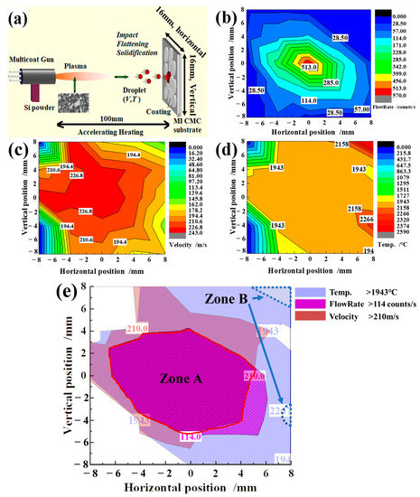
Figure 3.
Schematic diagrams of (a) the Si layer spraying process and (b–d) the properties of inflight Si particles measured in a 16 mm × 16 mm rectangle plane, 100 mm away from the spray gun. (e) Multi-contour map with several threshold values.
Figure 3d shows that the temperatures of the Si particles in most areas were between 1943 and 2158 °C. Particles at the highest temperatures (above 2266 °C) can be distinctly observed in two corners of the figure, rather than at the center. Figure 3e presents a multi-contour map with several threshold values to illustrate the surface morphology of the Si layer. In the plasma spraying process, Si particles with lower speeds and higher temperatures were more readily oxidized than faster-moving particles at lower temperatures. Based on the results presented in Figure 3b–e, it is reasonable to conclude that most particles in Zone A represented the part of the coating where there was less oxidation. Contrarily, a few tiny particles in Zone B were heated to a higher temperature, and these tended to create more heavily oxidized particles, as illustrated in Figure 2b.
In addition, XRD was used to test the phase composition of the Si layers, and Figure 4 shows the typical pattern of the coating prepared using the parameter of P0. We found that all the deposited coatings were cubic polysilicon, and that there was no phase transformation in the different parameters studied in this work. The peaks of silica were not clear in the coatings. Considering the EDS results, there was only slight oxidation of the Si layer, which is mostly amorphous.
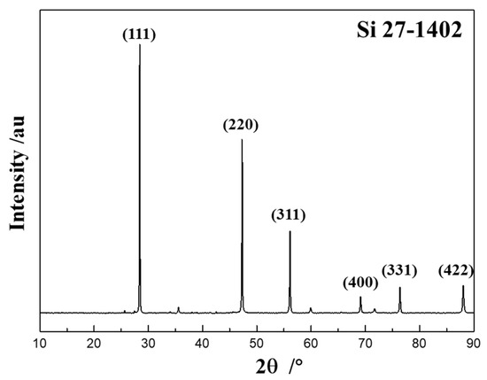
Figure 4.
XRD pattern of the Si layer sprayed using the parameter of P0.
3.2. The Influence of Spraying and Annealing Parameters on the Residual Surface Stress
Because APS Si layers are polysilicon films, the values of = 160 GPa and = 0.22 were adopted in this study, following the study in [35]. In addition, the (422) plane with a standard interplanar spacing of 1.1086 nm was selected due to its relatively strong intensity and higher 2θ. According to the Mn Kα (λ = 0.210314 nm), = 71.5348° for the (422) plane. Finally, was calculated to be , according to Equation (7). In this study, seven couples of – were detected for all samples, and the angles included −1.54°, 4.40°, 13.66°, 18.46°, 23.27°, 32.52°, and 38.47°. XRD surface stress measurement data for the basic parameter P0 are shown in Figure 5. The data were linearly fitted using the least squares method, and the stress was calculated to be 63.8 ± 14.6 MPa. When the residual stress is tensile for thermal-sprayed coatings, there is a stress perpendicular to the coating interface whose direction is away from the substrate; therefore, coating adhesion is poor. Once the tensile stress exceeds the interface bonding, the coating peels off. For this reason, it is necessary to reduce the tensile stress or adjust the compressive stress through parameter adjustment or after treatment.
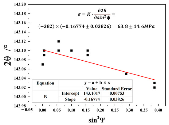
Figure 5.
XRD surface stress measurement data for the basic parameter of P0. The stress values corresponding to these data were obtained from the plot of versus .
Table 3 lists the calculated residual stress values for nine groups of coatings. Across all the investigated spraying parameters, the residual stresses on the surface of the Si bond layer ranged from 53.5 to 65.9 MPa, and all coatings exhibited tensile stress.
Table 3.
Calculated residual stresses for nine groups of coatings.
Figure 6 shows the influence of the spraying parameters on residual stress on the Si bond layer surfaces. The residual stress increased when the current rose from 330 to 380 A but, thereafter, decreased slightly when the current rose further to 430 A. The influence of the primary gas (Ar) on residual stress was similar to that of the current, reaching a maximum value at 35 nlpm. The effects of the second gas (H2) and spraying distance produced monotonous changes in residual stress. The stress value increased significantly when the hydrogen flow rate rose from 4 to 6 nlpm and increased, but more slowly, when the rate rose further from 6 to 8 nlpm. In contrast to the hydrogen flow rate, the spraying distance produced an opposite effect such that the residual stress decreased as the spraying distance increased.
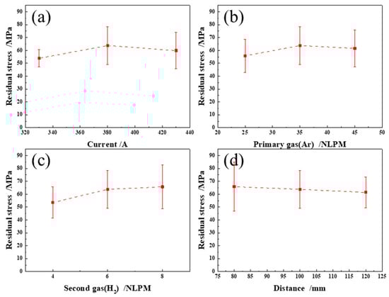
Figure 6.
Residual stress variation with differences in (a) current, (b) primary gas, (c) second gas, and (d) spraying distance.
Additionally, the reasons for the relatively large errors seen in this experiment were two-fold. Firstly, the sample was tested as-sprayed, with certain anisotropy, which affected the 2 measured at different angles. Secondly, the X-ray could penetrate to a depth of approximately 10 μm, and there was a stress gradient in the depth direction of the coating. In this part, the correlation study between surface stress and spraying parameter was simplified without considering the information on the depth and anisotropy.
When the plasma spraying parameters were adjusted, there were significant changes in the speeds and temperatures of the Si particles deposited on the CMC surface. The effects of changing the particle temperatures and velocities on the residual stress and other mechanical properties of the plasma-sprayed Al2O3 coating were studied in [36], where it was found that an increase in the particle temperature mainly led to a rise in the tensile stress. In our study, the temperatures and velocities of Si particles in the plasma flame were also measured and counted during plasma spraying to contribute to understanding the coating stress’s nature.
Figure 7 shows the temperature and velocity distributions of Si particles at different spraying distances. The results showed that the Si particles near the center of the flame were effectively accelerated, reaching 250 m/s when the spraying distance was 80 mm. When the spraying distance was increased to 100–120 mm, the particle velocity decreased slightly to approximately 225–250 m/s. Figure 7 also shows that, in contrast to the particle velocity distribution, the particles with the highest temperature were not distributed in the center of the flame. This finding could be explained by the fact that most of the particles were concentrated at the center, but the average heat received by every single particle was relatively low, resulting in temperatures ranging from 2000–2250 °C. As the spraying distance increased, the temperature of most particles in the central area gradually decreased, reaching around 1750–2250 °C when the spraying distance was 120 mm. According to the results shown in Figure 6d and Figure 7, we concluded that the decrease in residual tensile stress in the coating was a result of the reduced temperature of the Si particles.
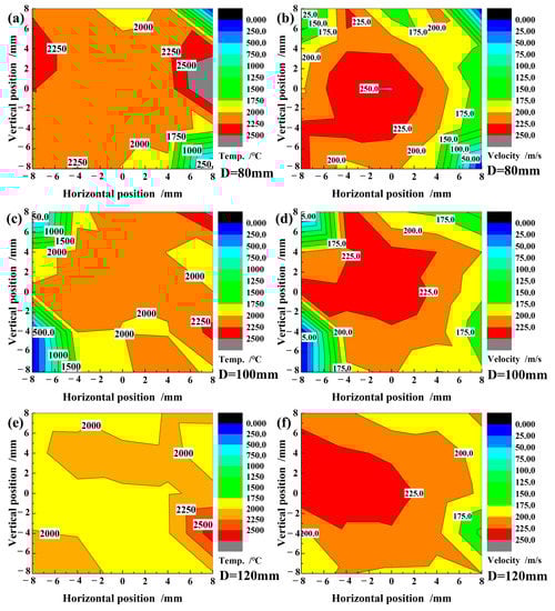
Figure 7.
Distribution of temperatures and velocities with different spraying distances: (a,b) 80 mm; (c,d) 100 mm; (e,f) 120 mm.
Figure 8 shows the influence of spraying parameters on the temperature and velocity of Si particles. With increases in current and primary gases (Ar), the velocities and temperatures of the particles exhibited monotonic increasing trends. When the current was increased from 330 to 430 A, the particle temperature and speed also increased from 2037 to 2057 °C and from 221 to 250 m/s, respectively. When the primary gas (Ar) flow rate rose from 25 to 45 NLPM, the particle temperature and speed increased from 2037 to 2062 °C and from 186 to 250 m/s, respectively. The particle temperature was positively correlated with the flow rate of the second gas (H2), increasing from 2038 to 2083 °C when the flow rate rose from 4 to 8 NLPM, but with only slight changes in the particle velocity (233–240 m/s). Finally, the particle velocity and temperature exhibited a decreasing trend with increased spraying distance, so when the distance rose from 80 to 120 mm, the temperature decreased from 2079 to 1981 °C, and the speed fell from 250 to 232 m/s.
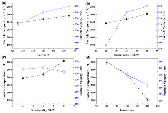
Figure 8.
Temperature and velocity variations with differences in (a) current, (b) primary gas, (c) second gas, and (d) spraying distance.
Combining the variations in residual stress, temperature, and velocity with the different parameters shown in Figure 6 and Figure 8, we found that the residual stress of the coating exhibited a greater correlation with the particle temperature within the range of the investigated parameters. In short, there was high residual tensile stress when the temperature rose, a result similar to that reported in [36]. An analysis of the data presented in Figure 8 indicated that the temperatures of Si particles were more sensitive to the parameters of spraying distance and flow rate of the second gas (H2). In contrast, the speeds of Si particles were more sensitive to the primary gas (Ar) flow rate. In other words, the parameters of spraying distance and the second gas (H2) flow rate could significantly affect the temperatures of Si particles but had little effect on particle velocity. Therefore, the spraying distance and the second gas (H2) flow rate could be considered the most important parameters for controlling residual stress on the coating surface.
The annealing process can be effectively optimized to eliminate the residual stress of the components. Zhang et al. [26] investigated the effects of regular furnace annealing on the residual stress of LPCVD polysilicon thin film. The results showed that after annealing at temperatures varying from 600 to 1100 °C, the film stress decreased gradually with increasing temperature. Additionally, the compressive stress varied very little with annealing time from 30 to 120 min. In this study, several prepared Si layers were heat-treated under an atmospheric environment, with the parameters shown in Table 4. The residual surface stresses of the resulting coatings were also evaluated using the sin2ψ method.
Table 4.
Summary of the annealing parameters of the Si layer.
Figure 9 shows the variations in the residual surface stress with different annealing temperatures and times. It can be seen that when the sample was annealed at 500 °C for 1 h and 5 h, the stress was slightly reduced from 68.9 MPa to 65.8 and 60.3 MPa. When the annealing temperature reached 800 °C, the coating stress level decreased rapidly to 66.5 MPa and changed from tensile to compressive at −4.1 MPa after 5 h. When the annealing temperature increased to 1100 °C, the residual stress on the Si layer surface transformed from a tensile stress of 56.2 MPa into a compressive stress of −45.2 MPa after 1 h, then stabilized over time. The same phenomenon was also observed for the annealing temperature of 1200–1300 °C. Hence, we concluded that for the Si coating sprayed on the SiC-CMCs, annealing can be carried out above 800 °C to eliminate tensile stress and thus promote the bonding of the coating with the substrate.
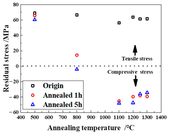
Figure 9.
Residual stress (tested using the sin2ψ method) variations with differences in annealing temperatures and times.
Figure 10 shows the XRD measurements of the as-sprayed and annealed silicon coatings. The results indicated that the deposited layers were cubic polysilicon, and no phase change occurred during the annealing process at a temperature up to 1300 °C. It can be seen that the intensity of the (400), (331), and (422) diffraction peaks increased significantly after annealing, compared to those of the as-sprayed Si layers. The enhancement in diffraction peaks may contribute to the changes in residual stress.
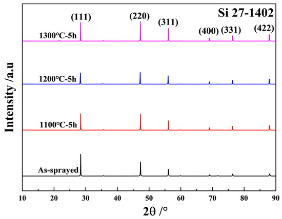
Figure 10.
XRD measurements of the as-sprayed and annealed silicon coatings.
3.3. Quantification and Distribution of Cross-Section Residual Stress
Six typical coatings were selected to test the residual surface stress via a combination of X-ray diffraction and Raman spectroscopy, as shown in Table 5. Figure 11 shows the residual stress–Raman shift results, with linear fitting according to the least squares method. Using Equation (5), the Raman shift–stress coefficient () and the Raman shift with free stress () were calculated as −201.41 MPa/cm−1 and 520.591 cm−1, respectively. The residual stress in the APS Si layer cross-section was then calculated using Equation (8):
Table 5.
Measurements of residual stress and Raman shift in typical coatings.
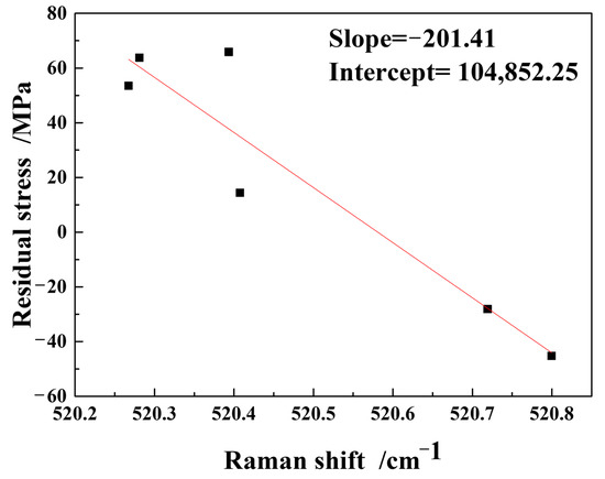
Figure 11.
Results of residual stress–Raman shift and linear fitting.
Figure 12 shows cross-sectional BSE-SEM images of the as-sprayed silicon layer. Using the APS process, a uniform and complete silicon coating on the SiC-CMCs was obtained, with some randomly distributed pores. No apparent defects at the coating/substrate interface were observed. The Raman test and stress calculation, as well as the determination of the coating thickness (shown in Figure 12) of the as-sprayed and heat-treated coatings, were carried out in this study according to Equation (8), and the results are shown in Figure 13.
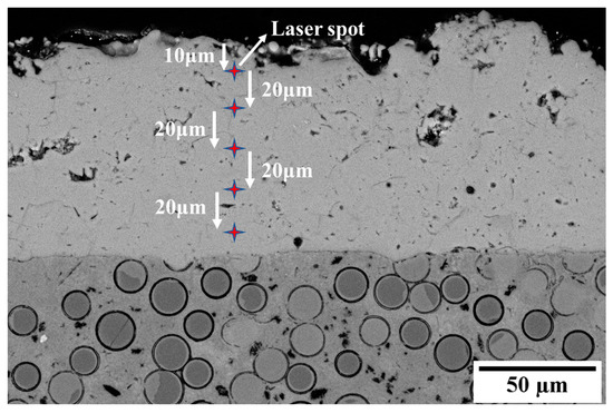
Figure 12.
BSE-SEM image of the as-sprayed silicon layer and schematic diagram showing the positions measured using Raman spectroscopy.
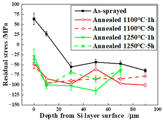
Figure 13.
Residual stress variations along the depth of the as-sprayed and annealed Si layer.
The surface of the as-sprayed Si layer exhibited residual tensile stress. However, the residual stress changed into compressive stress at a depth of 10–20 μm and then stabilized along the coating thickness. Compressive stress of 64 MPa appeared near the interface of the silicon layer and SiC-CMCs. This value was slightly higher than the residual stress of the silicon layer reported in [37].
Additionally, residual stress distribution was evaluated in the cross-section of the Si layer annealed at 1100 and 1250 °C, as shown in Figure 13. The surface and interior of the coating both exhibited compressive stress after heat treatment, with the stress values lowest near the coating surface. Compared with the as-sprayed layer, the compressive stress in the coating increased more considerably, but there was no obvious difference between 1100 and 1250 °C. Furthermore, the high-temperature treatment reduced the stress difference between the surface and the interior of the APS silicon layers, resulting in uniform residual stress throughout the coating area.
4. Conclusions
In this paper, Si layers were prepared on SiC-CMCs using APS technology and different parameters. The residual stress was tested and calculated by using X-ray sin2ψ technology coupled with laser Raman spectroscopy, and the microstructure and phase were also evaluated. The following conclusions were obtained:
- (1)
- The as-sprayed Si coatings prepared in this work exhibited tensile surface stress, ranging from 53.5 to 65.9 MPa. The spraying distance and the second gas (H2) flow rate could be considered the most important parameters for controlling residual stress on the coating surface.
- (2)
- When the annealing temperature reached 800 °C, the surface tensile stress of the as-sprayed Si coating level rapidly decreased and transformed into compressive stress after 5 hrs. This phenomenon occurred more quickly when the annealing temperature was higher than 1100 °C.
- (3)
- Using a combination of X-ray diffraction and Raman spectroscopy, the Raman shift–stress coefficient () and the Raman shift with free stress () were calculated as −201.41 MPa/cm−1 and 520.591 cm−1, respectively, for the APS Si layer.
- (4)
- Based on the calculated and values, the residual stress distribution in the cross-section of the Si layers was analyzed. Compared with the as-sprayed Si layer, the surface and interior of the coating both showed compressive stress after heat treatment at 1100 and 1250 °C.
Although some results were obtained, this study was preliminary, and more work needs to be carried out to achieve the control of residual stress accurately for APS Si coatings.
Author Contributions
M.G.: resources, investigation, data curation, writing—original draft, reviewing, and editing. Y.C.: conceptualization and methodology. C.W.: formal analysis. J.J.: funding acquisition. C.T.: supervision. X.B.: supervision. All authors have read and agreed to the published version of the manuscript.
Funding
This work was supported by the Science Center for Gas Turbine Project (Grant No. P2022-B-Ⅳ-003-001).
Institutional Review Board Statement
Not applicable.
Informed Consent Statement
Not applicable.
Data Availability Statement
Not applicable.
Conflicts of Interest
The authors declare no conflict of interest.
References
- Liu, J.; Zhang, L.; Liu, Q.; Cheng, L.; Wang, Y. Calcium–magnesium–aluminosilicate corrosion behaviors of rare-earth disilicates at 1400 °C. J. Eur. Ceram. Soc. 2013, 33, 3419–3428. [Google Scholar] [CrossRef]
- Glass, D. Ceramic Matrix Composite (CMC) Thermal Protection Systems (TPS) and Hot Structures for Hypersonic Vehicles. In Proceedings of the 15th AIAA International Space Planes and Hypersonic Systems and Technologies Conference, Dayton, OH, USA, 28 April–1 May 2008. [Google Scholar]
- Katoh, Y.; Snead, L.; Henager, C.; Nozawa, T.; Hinoki, T.; Iveković, A.; Novak, S.; de Vicente, S.G. Current status and recent research achievements in SiC/SiC composites. J. Nucl. Mater. 2014, 455, 387–397. [Google Scholar] [CrossRef]
- Christin, F. Design, Fabrication, and Application of Thermostructural Composites (TSC) like C/C, C/SiC, and SiC/SiC Composites. Adv. Eng. Mater. 2002, 4, 903–912. [Google Scholar] [CrossRef]
- Beesley, C. The Application of CMCs in High Integrity Gas Turbine Engines. Key Eng. Mater. 1996, 127–131, 165–176. [Google Scholar] [CrossRef]
- Tejero-Martin, D.; Bennett, C.; Hussain, T. A review on environmental barrier coatings: History, current state of the art and future developments. J. Eur. Ceram. Soc. 2021, 41, 1747–1768. [Google Scholar] [CrossRef]
- Padture, N.P. Environmental degradation of high-temperature protective coatings for ceramic-matrix composites in gas-turbine engines. Npj Mater. Degrad. 2019, 3, 11. [Google Scholar] [CrossRef]
- Jian, Y.; Wang, Y.; Liu, R.; Wan, F.; Zhang, J. Property evolutions of Si/mixed Yb2Si2O7 and Yb2SiO5 environmental barrier coatings completely wrapping up SiCf/SiC composites under 1300 °C water vapor corrosion. Ceram. Int. 2021, 47, 22373–22381. [Google Scholar] [CrossRef]
- Chen, H.-F.; Zhang, C.; Liu, Y.-C.; Song, P.; Li, W.-X.; Yang, G.; Liu, B. Recent progress in thermal/environmental barrier coatings and their corrosion resistance. Rare Met. 2020, 39, 498–512. [Google Scholar] [CrossRef]
- Jang, B.-K.; Feng, F.-J.; Lee, K.-S.; García, E.; Nistal, A.; Nagashima, N.; Kim, S.; Oh, Y.-S.; Kim, H.-T. Thermal behavior and mechanical properties of Y2SiO5 environmental barrier coatings after isothermal heat treatment. Surf. Coat. Technol. 2016, 308, 24–30. [Google Scholar] [CrossRef]
- Cojocaru, C.V.; Kruger, S.E.; Moreau, C.; Lima, R.S. Elastic Modulus Evolution and Behavior of Si/Mullite/BSAS-Based Environmental Barrier Coatings Exposed to High Temperature in Water Vapor Environment. J. Therm. Spray Technol. 2011, 20, 92–99. [Google Scholar] [CrossRef]
- Cojocaru, C.; Lévesque, D.; Moreau, C.; Lima, R.S. Performance of thermally sprayed Si/mullite/BSAS environmental barrier coatings exposed to thermal cycling in water vapor environment. Surf. Coat. Technol. 2013, 216, 215–223. [Google Scholar] [CrossRef]
- Lee, K.N.; Eldridge, J.I.; Robinson, R.C. Residual Stresses and Their Effects on the Durability of Environmental Barrier Coatings for SiC Ceramics. J. Am. Ceram. Soc. 2005, 88, 3483–3488. [Google Scholar] [CrossRef]
- Samal, S.; Molnárová, O.; Pruša, F.; Kopecek, J.; Heller, L.; Šittner, P.; Škodová, M.; Abate, L.; Blanco, I. Net-Shape NiTi Shape Memory Alloy by Spark Plasma Sintering Method. Appl. Sci. 2021, 11, 1802. [Google Scholar] [CrossRef]
- Samal, S.; Tyc, O.; Cizek, J.; Klecka, J.; Luká, F.; Molnárová, O.; de Prado, E.; Weiss, Z.; Kopecek, J.; Heller, L.; et al. Fabrication of Thermal Plasma Sprayed NiTi Coatings Possessing Functional Properties. Coatings 2021, 11, 610. [Google Scholar] [CrossRef]
- Samal, S.; Kopecek, J.; Šittner, P. Interfacial Adhesion of Thick NiTi Coating on Substrate Stainless Steel. Materials 2022, 15, 8598. [Google Scholar] [CrossRef]
- Harder, B.J.; Almer, J.D.; Weyant, C.M.; Lee, K.N.; Faber, K.T. Residual Stress Analysis of Multilayer Environmental Barrier Coatings. J. Am. Ceram. Soc. 2009, 92, 452–459. [Google Scholar] [CrossRef]
- Du, J.; Liu, R.; Wan, F.; Li, D.; Li, J.; Wang, Y. Failure mechanism of ytterbium silicate/silicon bi-layer environmental barrier coatings on SiCf/SiC composites upon long-time water vapor and oxygen corrosion test. Surf. Coat. Technol. 2022, 447, 128871. [Google Scholar] [CrossRef]
- Du, J.; Yu, G.; Jia, Y.; Liu, C.; Sui, Z.; Gao, X.; Wang, F.; Song, Y. Numerical study of residual stresses in environmental barrier coatings with random rough geometry interfaces. Ceram. Int. 2023, 49, 5748–5759. [Google Scholar] [CrossRef]
- Talaat, H.; Negm, S.; Schaffer, H.; Kaltsas, G.; Nassiopoulou, A. Micro-Raman analysis of polysilicon membranes deposited on porous silicon channels. J. Non-Crystalline Solids 2000, 266–269, 1345–1349. [Google Scholar] [CrossRef]
- Nguyen, T.N.; Nguyen, V.D.; Jung, S.; Yi, J. Raman scattering analysis of the residual stress in metal-induced crystallized amorphous silicon thin films using nickel. Appl. Surf. Sci. 2009, 255, 8252–8256. [Google Scholar] [CrossRef]
- Zheng, L.; Zhao, G.; Yan, C.; Xu, X.; Su, L.; Dong, Y.; Xu, J. Raman spectroscopic investigation of pure and ytterbium-doped rare earth silicate crystals. J. Raman Spectrosc. 2007, 38, 1421–1428. [Google Scholar] [CrossRef]
- Li, X.; Jin, S.; Zhang, R.; Gao, Y.; Liu, Z.; Yao, Y.; Wang, Y.; Wang, X.; Zhang, Y.; Tao, X. The resolution and repeatability of stress measurement by Raman and EBSD in silicon. Vacuum 2022, 203, 111276. [Google Scholar] [CrossRef]
- Cui, Y.; Guo, M.; Wang, C.; Tang, Z.; Cheng, L. Evolution of the residual stress in porous ceramic abradable coatings under thermal exposure. Surf. Coat. Technol. 2020, 394, 125915. [Google Scholar] [CrossRef]
- Cui, Y.; Guo, M.; Wang, C.; Jiao, J.; Cheng, L. Zirconia-based Abradable Coatings Fabricated on Single-crystal Superalloy: Microstructure, Residual Stress and Mechanical Properties. J. Alloys Compd. 2022, 907, 164537. [Google Scholar] [CrossRef]
- Zhang, X.; Zhang, T.-Y.; Wong, M.; Zohar, Y. Residual-stress relaxation in polysilicon thin films by high-temperature rapid thermal annealing. Sensors Actuators A Phys. 1998, 64, 109–115. [Google Scholar] [CrossRef]
- Teixeira, R.; Doi, I.; Zakia, M.; Diniz, J.; Swart, J. Micro-Raman stress characterization of polycrystalline silicon films grown at high temperature. Mater. Sci. Eng. B 2004, 112, 160–164. [Google Scholar] [CrossRef]
- Kang, Y.; Qiu, Y.; Lei, Z.; Hu, M. An application of Raman spectroscopy on the measurement of residual stress in porous silicon. Opt. Lasers Eng. 2005, 43, 847–855. [Google Scholar] [CrossRef]
- Li, Q.; Qiu, W.; Tan, H.; Guo, J.; Kang, Y. Micro-Raman spectroscopy stress measurement method for porous silicon film. Opt. Lasers Eng. 2010, 48, 1119–1125. [Google Scholar] [CrossRef]
- Mauer, G.; Vaßen, R.; Zimmermann, S.; Biermordt, T.; Heinrich, M.; Marques, J.-L.; Landes, K.; Schein, J. Investigation and Comparison of In-Flight Particle Velocity During the Plasma-Spray Process as Measured by Laser Doppler Anemometry and DPV-2000. J. Therm. Spray Technol. 2013, 22, 892–900. [Google Scholar] [CrossRef]
- Guo, X.; Planche, M.-P.; Chen, J.; Liao, H. Relationships between in-flight particle characteristics and properties of HVOF sprayed WC-CoCr coatings. J. Mater. Process. Technol. 2014, 214, 456–461. [Google Scholar] [CrossRef]
- Ye, C.; Jiang, P. Accurate residual stress measurement as a function of depth in environmental barrier coatings via a combination of X-ray diffraction and Raman spectroscopy. Ceram. Int. 2020, 46, 12613–12617. [Google Scholar] [CrossRef]
- Kouteva-Arguirova, S.; Seifert, W.; Kittler, M.; Reif, J. Raman measurement of stress distribution in multicrystalline silicon materials. Mater. Sci. Eng. B 2003, 102, 37–42. [Google Scholar] [CrossRef]
- Niu, Y.; Zheng, X.; Liu, X.; Ji, H.; Ding, C. Influence of powder size on characteristics of air plasma sprayed silicon coatings. Ceram. Int. 2012, 38, 5897–5905. [Google Scholar] [CrossRef]
- Hopcroft, M.A.; Nix, W.D.; Kenny, T.W. What is the Young’s Modulus of Silicon? J. Microelectromech. Syst. 2010, 19, 229–238. [Google Scholar] [CrossRef]
- Ghara, T.; Bandyopadhyay, P. Understanding the role of in-flight particle temperature and velocity on the residual stress depth profile and other mechanical properties of atmospheric plasma sprayed Al2O3 coating. J. Eur. Ceram. Soc. 2022, 42, 4353–4368. [Google Scholar] [CrossRef]
- Richards, B.T.; Begley, M.R.; Wadley, H.N. Mechanisms of Ytterbium Monosilicate/Mullite/Silicon Coating Failure During Thermal Cycling in Water Vapor. J. Am. Ceram. Soc. 2015, 98, 4066–4075. [Google Scholar] [CrossRef]
Disclaimer/Publisher’s Note: The statements, opinions and data contained in all publications are solely those of the individual author(s) and contributor(s) and not of MDPI and/or the editor(s). MDPI and/or the editor(s) disclaim responsibility for any injury to people or property resulting from any ideas, methods, instructions or products referred to in the content. |
© 2023 by the authors. Licensee MDPI, Basel, Switzerland. This article is an open access article distributed under the terms and conditions of the Creative Commons Attribution (CC BY) license (https://creativecommons.org/licenses/by/4.0/).