Article

Electrochemical Synthesis of a WO3/MoSx Heterostructured Bifunctional Catalyst for Efficient Overall Water Splitting

by
Ramūnas Levinas
1,2,*,
Natalia Tsyntsaru
1,3,
Henrikas Cesiulis
1,
Roman Viter
4,5,
Karlis Grundsteins
4,
Loreta Tamašauskaitė-Tamašiūnaitė
2 and
Eugenijus Norkus
2
1
Faculty of Chemistry and Geosciences, Vilnius University, 03225 Vilnius, Lithuania
2
State Research Institute, Center for Physical Sciences and Technology (FTMC), 10257 Vilnius, Lithuania
3
Institute of Applied Physics, Moldova State University, 2028 Chisinau, Moldova
4
Institute of Atomic Physics and Spectroscopy, University of Latvia, 1586 Riga, Latvia
5
Center for Collective Use of Scientific Equipment, Sumy State University, 40018 Sumy, Ukraine
*
Author to whom correspondence should be addressed.
Coatings 2023, 13(4), 673; https://doi.org/10.3390/coatings13040673
Submission received: 28 February 2023 / Revised: 21 March 2023 / Accepted: 23 March 2023 / Published: 25 March 2023

Abstract

:
Photo-/electrochemical water splitting can be a suitable method to produce “green” hydrogen and oxygen by utilizing renewable energy or even direct sunlight. In order to carry out photoelectrochemical (PEC) water splitting, a photoanode based on transition metal oxides, which absorbs photons and produces photoexcited electron–hole pairs, is needed. The positively charged holes can then participate in the water oxidation reaction. Meanwhile, a cathodic hydrogen evolution reaction (HER) can occur more efficiently with electrocatalytic materials that enhance the adsorption of H+, such as MoS2. In this study, it was shown that WO3/MoSx heterostructured materials can be synthesized by an electrochemical method called plasma electrolytic oxidation (PEO). During this process, many micro-breakdowns of the oxide layer occur, causing ionization of the oxide and electrolyte. The ionized mixture then cools and solidifies, resulting in crystalline WO3 with incorporated MoSx. The surface and cross-sectional morphology were characterized by SEM-FIB, and the coatings could reach up to 3.48 μm thickness. Inclusion of MoSx was confirmed by EDX as well as XPS. Synthesis conditions were found to have an influence on the band gap, with the lowest value being 2.38 eV. Scanning electrochemical microscopy was used to map the local HER activity and correlate the activity hotspots to MoSx’s content and surface topography. The bifunctional catalyst based on a WO3/MoSx heterostructure was evaluated for PEC and HER water-splitting activities. As a photoanode, it could reach up to 6% photon conversion efficiency. For HER in acidic media, a Tafel slope of 42.6 mV·dec−1 can be reached.

1. Introduction

In the near future, in order to drive certain industrial and technological processes, utilization of solar energy will become more widespread than ever. This is proven by economic outlook reports such as that issued by the International Energy Agency, Renewables 2022, which forecasts global solar photovoltaic capacity to triple over the period 2022–2027. Furthermore, solar energy is actively being investigated as a viable solution for such issues as CO2 reduction and water splitting to produce hydrogen [1,2]. Hydrogen in particular is a promising fuel for the future as it has the largest gravimetric current density of all known substances (~120 kJ·g−1) [3], and therefore could be used to power energy-intensive technologies. Admittedly, the use of liquid hydrogen as an energy carrier faces many fundamental problems, one of which is its production.
Nowadays, the production of hydrogen cannot be separated from the strive for climate neutrality. Although hydrogen can be produced in large quantities by steam methane reformation, it is classified as grey hydrogen due to the large carbon footprint of this process; this is in contrast to green hydrogen, which is synthesized using only renewable sources [4]. However, green hydrogen production processes (such as photoelectrochemical water splitting/electrolysis) are much less effective, thus the resulting hydrogen is more expensive and, as of yet, uneconomical [5].
The efficiency of solar light utilization in photoelectrochemical (PEC) processes is directly related to the band gap of the light absorbing material. The thermodynamic limit for the onset of water splitting is 1.23 eV, and the catalytic material should have a band gap close to this value. In reality, this is hardly achievable, but some transition metal oxides have a combination of properties that make them prime candidates for PEC catalysis. WO3 is one of these materials, as it has a band gap of ~2.7 eV, which can be further lowered by tuning the synthesis conditions or creating heterostructures with other materials [6,7,8]. In addition, WO3 is relatively stable under anodic conditions in acidic media, though it does undergo noticeable photo-corrosion in different electrolytes [9]. Photoactive WO3 films have been prepared through various methods such as hydrothermal [10,11] or sol-gel synthesis [12], magnetron sputtering [13], spray/aerosol pyrolysis [14,15], as well as electrochemically on the cathode [16,17,18] or anode [19,20]. A modification of anodic synthesis is plasma electrolytic oxidation (PEO), which has been used to grow transition metal oxide coatings and heterostructures [21,22,23].
Another material that is often used for electrochemical water splitting is molybdenum sulfide (MoS2) [24]. It is used as an electrocatalyst for hydrogen evolution reaction (HER)s in acidic media because of the favorable thermodynamics of H+ adsorption on the surface active sites [25]. The mechanism of HER on MoS2 is identical to that on Pt. Thus, MoS2 can be considered a non-precious metal electrocatalyst and an alternative to Pt [26]. It is also a semiconductor with a tunable band gap, averaging ~1.7 eV for 2H-MoS2 [27]. MoS2 has also been used in bifunctional catalysts to improve the HER activity of an oxygen evolution reaction (OER) catalyst [28]. Various methods have been developed to synthesize photoactive MoS2 structures [29], the more prominent being chemical vapor deposition (CVD) [30,31,32], wet chemical synthesis [33,34], and electrochemical deposition [35,36,37,38].
New materials based on WO3 and MoS2 have been synthesized by methods such as sol-gel spin coating, probe sonication, or wet chemical synthesis, and were tested for electrochromic devices [39], as sensors [40] and photocatalysts [41].
In this study, the possibility of depositing WO3 and MoS2 through a one-stage process, namely PEO, is investigated. Although this method has been known for decades, it is regaining attention in the scientific community [42,43]. PEO is an excellent method to produce transition metal oxide films with unique properties. It also provides the possibility to incorporate ions into the film. Therefore, a new bifunctional WO3/MoSx heterostructured catalyst was synthesized and comprehensively evaluated. The perspectives of this novel heterostructure, in which WO3 can act as a photoanode and the MoS2 as a lower band gap semiconductor, and the HER electrocatalyst were also assessed.

2. Materials and Methods

2.1. Plasma Electrolytic Oxidation Procedure

Tungsten plates (99.5%, Alfa Aesar, Ward Hill, MA, USA) were used as working electrodes with a geometrical area of 2 cm2. They were connected as the anode in a two-electrode cell, with a stainless steel coil as the counter electrode. The WO3/MoSx heterostructures were obtained from the following electrolytes: 1 M Na2SO4 (≥99%, Roth, Karlsruhe, Germany), 75 mM NaF (≥99%, Roth), 0.1 M NaH2PO2 (≥99%, Roth), and 25 mM of MoS42−. The last component was synthesized from (NH4)6Mo7O24·4H2O (≥99%, Roth) and 60% Na2S (Roth). WO3 films were also obtained from the same bath, but without MoS42− for comparison. The syntheses were carried out at room temperature (22 ± 3 °C) under galvanostatic conditions (Consort EV245, Cleaver Scientific, Rugby, Warwickshire, UK) power supply) by applying current of 50 mA. The solution was agitated with a magnetic stirrer. In order to evaluate the influence of the targeted properties, the duration of synthesis was 2, 5 and 30 min. The tags 2-min, 5-min, and 30-min WO3 or WO3/MoSx were assigned, respectively.

2.2. Structural Characterization

An FEI Helios Nanolab 650 (Hillsboro, OR, USA) dual beam system with an energy dispersive X-ray (EDX) spectrometer INCA Energy 350 (Oxford Instruments, Abingdon, Oxfordshire, UK) and X-Max 20 mm2 (Oxford Instruments, Abingdon, Oxfordshire, UK) detector was used to observe the surface morphology by scanning electron microscopy and EDX mapping. A Ga+ ion beam was used for focused ion beam (FIB) analysis. The XPS analyses were carried out with a Kratos Axis Supra spectrometer (Kratos Analytical Limited, Manchester, UK) using a monochromatic Al K(alpha) source (25 mA, 15 kV). Survey scan analyses were carried out on the area of 300 μm × 700 μm at a pass energy of 160 eV. High-resolution analyses were carried out also on the area of 300 μm × 700 μm, but at a pass energy of 20 eV. The XPS signal due to adventitious carbon located at 284.8 eV was used as a binding energy (BE) reference. An X-ray diffractometer (D2 Phaser, Bruker, Billerica, MA, USA, λ = 1.5418 Å/Cu Kα) was used to characterize the crystal structure of the obtained films.

2.3. Optical Properties

Diffuse reflectance spectra were measured in the range of 250–900 nm by means of an Ocean Optics HR4000 spectrometer (Ocean Insight, Orlando, FL, USA), Ocean Optics reflectance probe (angle 45°) and deuterium–halogen light source (DH-2000-BAL, Ocean Insight, Orlando, FL, USA). Diffuse reflectance R was converted to absorbance F using the following known Kubelka–Munc equation:
F = ( 1 R ) 2 2 · R
Band gap Eg was graphically calculated from the following equation:
( F · h v ) 1 / 2 = A ( h v E g )

2.4. Photo-/Electrochemical Characterization and Electrochemical Treatment

All photo- and electrochemical measurements were carried out by means of an Autolab 302 N (Metrohm, Utrecht, The Netherlands) potentiostat connected to an Autolab optical bench system. A 365 nm LED (Thorlabs, Newton, NJ, USA) was used for photoexcitation, with the light intensity calibrated to 25 mW cm−2. The photoelectrochemical (PEC) properties of synthesized films were evaluated in a quartz three-electrode cell with a Ag/AgCl reference electrode and a stainless steel counter electrode. The HER characterization was carried out in a regular 3-electrode glass cell. An electrochemical reduction-activation treatment was carried out to prove the possibility of further improving the PEC properties of the heterostructures. Specific experimental steps are summarized in Table 1, and have been described in detail recently [44,45]. The potential values were recalculated vs. RHE, and are presented as such throughout the study, unless it is stated otherwise.
The relationship between incident light intensity (I0) and photon conversion efficiency was also evaluated by measuring potentiostatic light pulses at 1.53 V, but under different I0, from 5 mW cm−2 to 30 mW cm−2. Obtained photocurrent values were recalculated to incident photon conversion efficiencies (IPCE) by Equation (3):
I P C E   ( % ) = j p h ( m A   cm 2 ) × 1240 ( V   nm ) I 0 ( m W   cm 2 ) × λ ( nm )

2.5. Scanning Electrochemical Microscopy (SECM)

SECM measurements were carried out using a Versa SCAN (Ametek, Berwyn, PA, USA) workstation connected with Versta STAT 3 and Versa STAT 3F bipotentiostat setup (Princeton Applied Research, Oak Ridge, TN, USA). The mode of operation was substrate generation/tip collection (SG/TC), wherein the substrate (WO3/MoSx heterostructures) was a generator, and the tip (25 μm Pt) was a collector. The substrate was immersed in 0.5 M H2SO4 solution. Before measurement, the substrates were subjected to an equilibration treatment by applying a −0.3 mA·cm−2 current for 20 min until a stable overpotential related to HER is reached. After suitable conditions were reached, the probe was lowered to ~15–25 μm of the substrate by a typical approach curve method. Then, the probe was polarized to 0 V (vs. Ag/AgCl), which had been determined to give a good hydrogen oxidation signal, and a 2D map was obtained by scanning the probe at a speed of 100 µm s−1 and measuring data points at 25 μm increments.

3. Results and Discussion

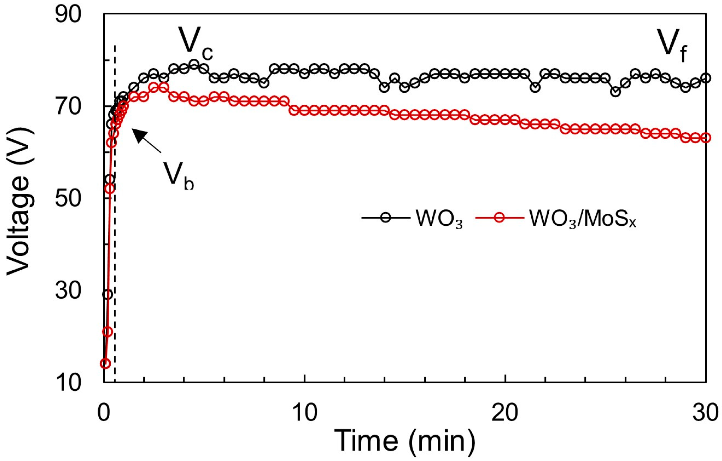
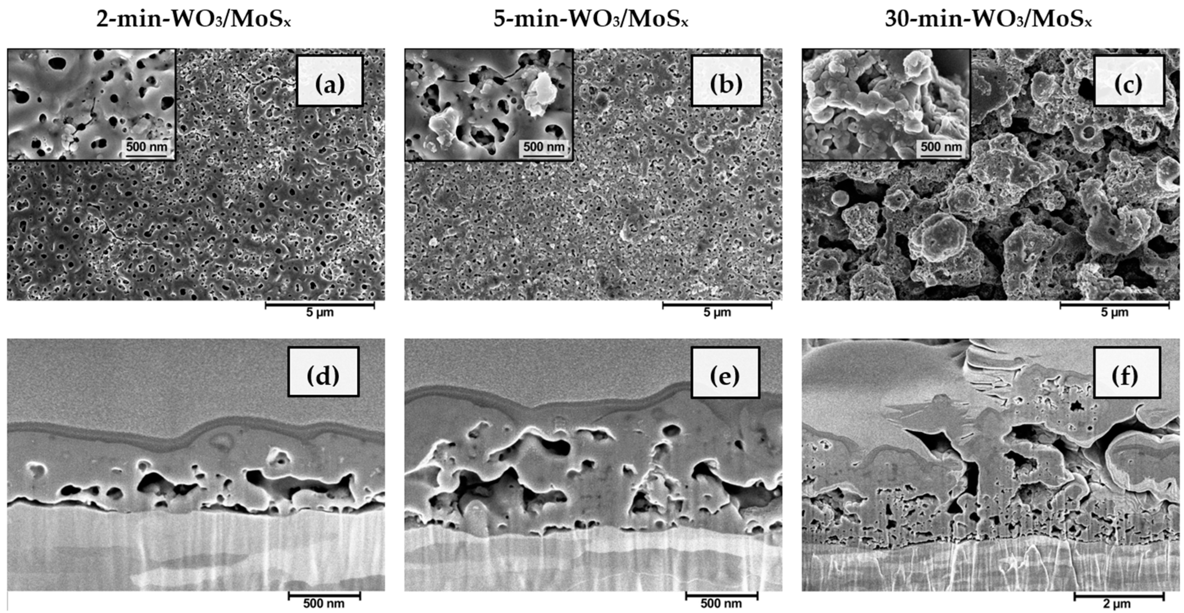
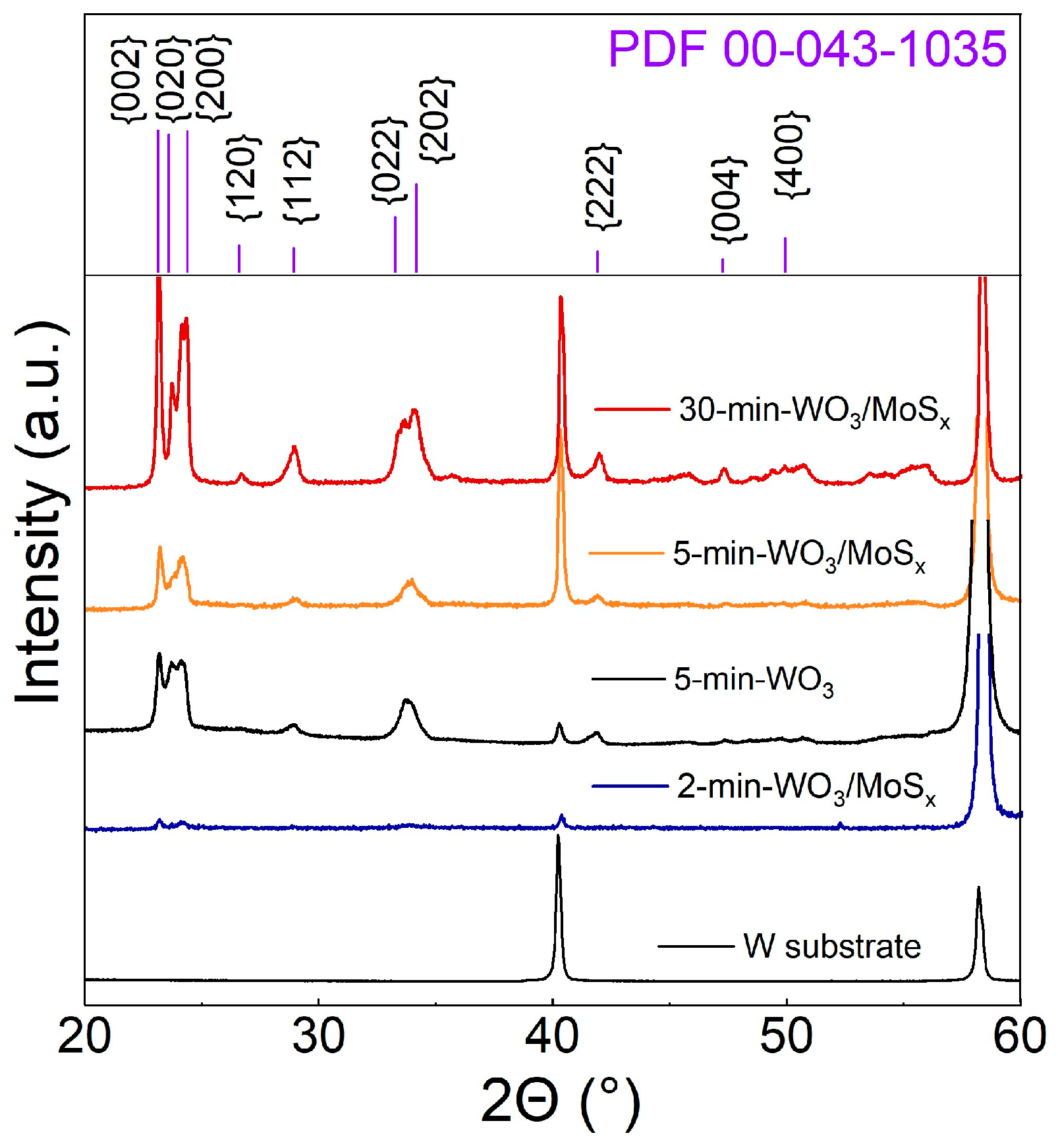
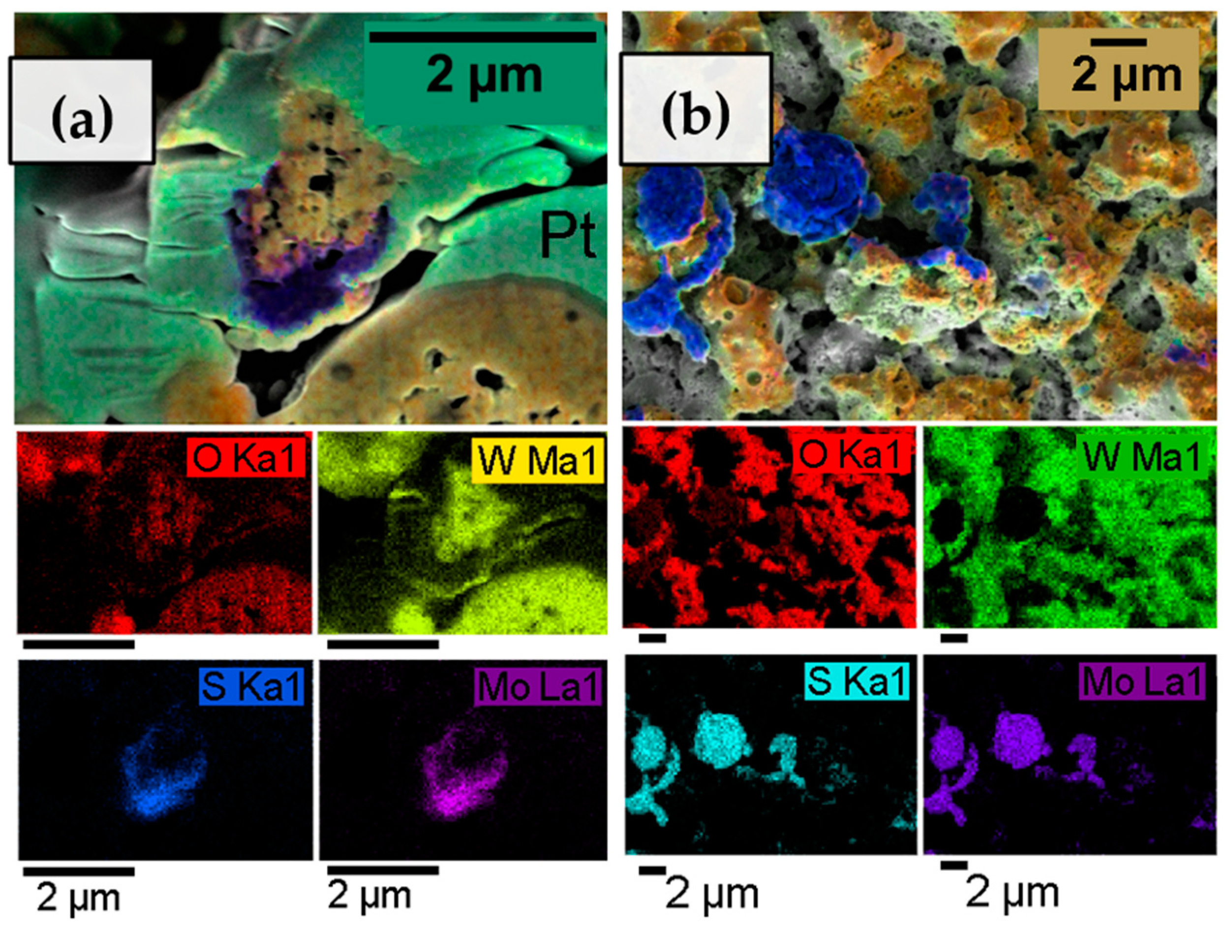
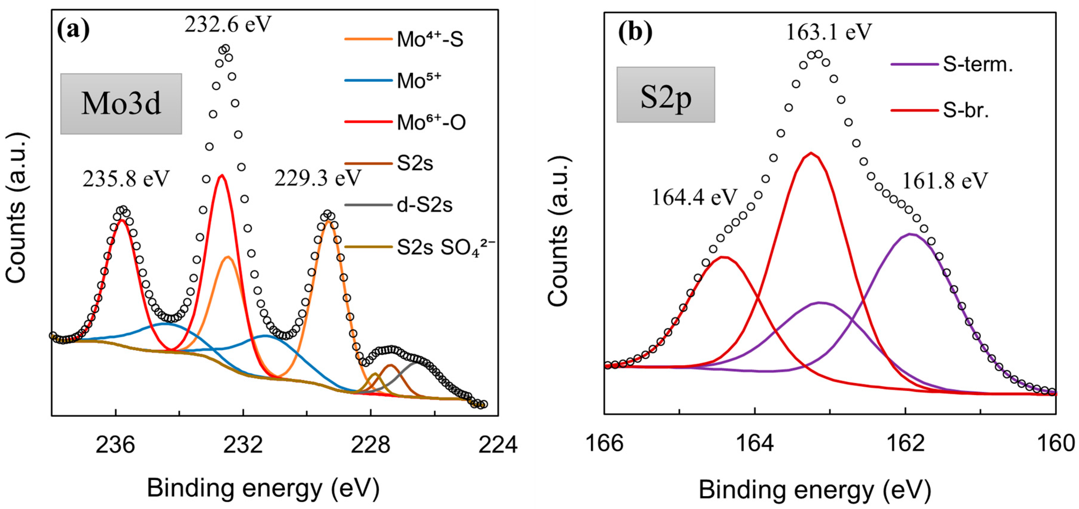
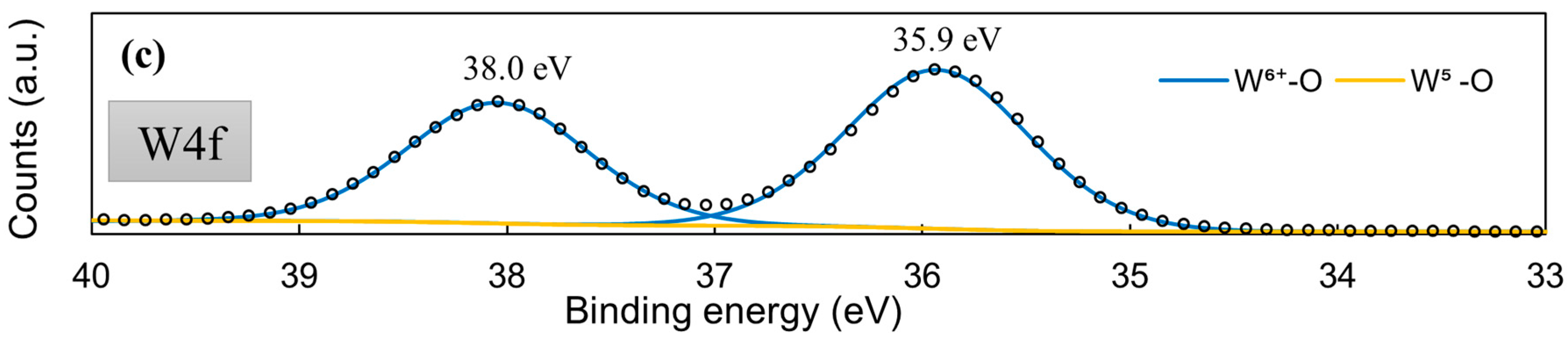
3.1. Synthesis and Structural Characterization of Heterostructures

PEO can be characterized by measuring the change of voltage with time under galvanostatic conditions. Similarly to TiO2 [46,47], the WO3 formation process (Figure 1) undergoes three consecutive stages. At the beginning of oxidation, voltage increases almost linearly with time, and the conventional anodic oxidation of W occurs. The growth of the anodic WO3 can be represented by the three-step process (Equations (4)–(6)), wherein metallic W is electrochemically dissolved and interacts with water from the solution to form WO3 film [48]:
W + 2 H 2 O WO 2 2 + + 4 H + + 6 e
WO 2 2 + + 2 H 2 O W 2 O 5 + 2 H +
W 2 O 5 + H 2 O 2 WO 3 + 2 H + + 2 e
In this stage, the voltage increases rapidly to maintain the applied current as the oxide layer grows, although some current is consumed for oxygen gas evolution. Notably, the obtained slopes of the V-t curves are very steep for both WO3 and WO3/MoSx, and the value of ~65 V is reached within 0.5 s (~130 V s−1). For comparison, the slopes observed for TiO2 in various electrolytes were 24 to 35 V s−1 [47]. It has been proposed that the voltage at the end of stage I is called the “breakdown voltage” (Vb), which in this case is approximately 65 V for both WO3 and the heterostructure. This is much lower than that for TiO2, but it is expected because WO3 is a less dielectric material.
When Vb is reached, the second oxidation stage begins, in which the slope of V-t decreases and tiny electric sparks generate the micro-breakdowns in the film. Now, the total current is governed by two components: the ionic current and the electric current. Due to this reason, a lower voltage is needed to maintain the applied current. The voltage may still increase until Vc (critical voltage), where Vc = 79 V for WO3 and Vc = 74 V for the WO3/MoSx heterostructure.
In stage III, the voltage values are almost constant and approach the final voltage (Vf). This is the case for WO3, and it means that the film has attained a constant resistance. However, for WO3/MoSx, the voltage drops from a maximum Vc = 74 V to Vf = 63 V. Because a lower voltage is needed to maintain the applied current, the films become more conductive when MoS2 is incorporated. Notably, ions from the electrolyte can be incorporated into the film during PEO because of complex chemical, electrochemical, and physical processes that occur during this process [49]. To generalize, electron avalanches during micro-breakdowns ionize both the oxide and electrolyte, and a mixture is formed and then solidifies again. However, in this particular case of MoS2, the anodic formation of MoS3 can also occur by disproportionation of MoS42− [50,51], by reaction 7, as proposed in [52]:
MoS 4 2 MoS 3 + 1 8 S 8 + 2 e
For further characterization, the heterostructured films were synthesized by capping PEO time to match the different stages: 2 min to reach Vb, 5 min when Vb is passed and value of Vc is reached, and 30 min for Vf. The surface and bulk morphologies of the obtained materials are shown in Figure 2, and are similar to those obtained for the plain WO3 that had been formed by a similar method [45] The films synthesized for 2 and 5 min are disorderedly nanoporous, with surface pore diameters apparently ranging up to several hundred nanometers (Figure 2a,b). Such pores are also sometimes called “discharge channels”. In addition, it is evident from the cross-sections of the respective samples (Figure 2d,e) that the channels do not propagate vertically from the substrate, as would be expected in a typical anodic tungsten oxide structure. On the contrary, the cavities within the growing material seem to preferentially propagate horizontally. This is the result of the PEO mechanism of oxide layer growth. At certain locations, film breakdown occurs and the electron avalanche flowing between the metallic W substrate and the film–electrolyte interface ionizes the oxide with some amount of electrolyte and causes a vapor blowout, leaving behind a cavity and ionized plasma mixture. The plasma is then cooled by the electrolyte, hardening and forming a pore. It is also worth distinguishing the film, obtained after 30 min (Figure 2c,f), the morphology of which is much rougher, although it was shaped by the same fundamental processes, only for a much longer duration. The average thickness of the films is linearly dependent on synthesis time, and ranges from 0.56 μm (±0.13 μm) to 3.48 μm (±1.1 μm) as the synthesis duration is increased from 2 to 30 min.
The crystalline nature of the films was revealed by XRD. Typically, non-annealed WO3 films that had been obtained by anodization are amorphous [53], but in this case, the diffractograms show that the peaks correspond to a monoclinic WO3 structure, wherein the (002), (020), and (200) peak intensities have similar proportions for all coatings (Figure 3). The relative intensities of monoclinic WO3 peaks are larger for thicker films, and distinct W substrate peaks are also detected for all samples. This is due to the X-ray penetration depth, because a stronger substrate signal and weaker oxide signal are seen for thinner films. All of the films, regardless of synthesis time, have a monoclinic structure. This is yet another effect of the PEO mechanism of oxide film growth; although no external heat is applied, the plasma caused by electric discharges produces enough energy to electrodeposit a crystalline material. Small peaks at the 2θ range of 50° to 60° that could not be attributed to WO3 appear on the diffractogram of the thickest film. Peaks at such 2θ values have been observed for hexagonal and synthesized MoS2 [54,55]. The weak signal is most likely related to the small amount of incorporated MoSx and the amorphous-like structure of it.
In the structural characterization of these heterostructured materials, it is important to investigate how MoS2 is dispersed throughout the WO3 matrix. For this purpose, the films of a WO3/MoSx sample deposited for 30 min were examined by an EDX mapping technique, which was carried out for areas on an FIB channel cross-section (Figure 4a) and top-down surface (Figure 4b). A strong tungsten signal was obtained, and the quantity of W correlates with O, suggesting the existence of a tungsten trioxide. The presence of Mo and S was also confirmed, but the excitation energies for these materials overlap in EDX analysis, so no definite quantitative conclusions could be drawn. However, the maps show that the MoS2 material is detected on the surface of the electrode in larger chunks of micrometer-order diameters. Cross-sectional EDX maps were also obtained for the thinner films (synthesized for 2 and 5 min), but no discernible Mo or S signal could be obtained.
Although the signal of Mo and S was not always strong enough for mapping, EDX data obtained for top-down areas of the samples show that Mo, S, and P are detected in the film. Up to ~1.5 % of P is detected in the films, and the amount does not vary with deposition time. P is incorporated into the film from H2PO2, as plasma discharges ionize the oxide and electrolyte and later cool down to a solid material. As for Mo and S, both materials are detected in the elemental composition of the films, but not in any expected stoichiometries such as MoS2 or MoS3. In fact, the apparent composition of MoSx is severely sulfur-deficient (e.g., MoS0.4 for 5-min-WO3/MoSx). This probably occurs due to molybdenum sulfide oxidation to some degree under anodic deposition conditions.
XPS was used to check whether the MoSx material is in fact comprised from Mo-S bonds. The core-level Mo3d XPS spectrum (Figure 5a) displayed the same characteristic peaks that had been observed for MoS2 synthesized by other methods [56,57], particularly for cathodically electrodeposited MoS2 [44]. The Mo3d region deconvolutes into several doublets that are related to Mo6+-O bonds (3d5/2 232.7 eV; 3d3/2 235.7 eV), Mo4+-S bonds (3d5/2 229.3 eV; 3d3/2 232.1 eV), and a Mo5+ signal, which may be related to a heptavalent oxide, but also to sulfur-deficient Mo/active sites (3d5/2 230.9 eV; 3d3/2 234.2 eV). Interestingly, the S2p core-level spectra (Figure 5b) deconvolute into two clear doublets, the existence of which can be attributed to terminal (S-term. S2p3/2 161.8 eV; Sp1/2 163.0 eV) and bridging (S-br. S2p3/2 163.2 eV; S2p1/2 164.2 eV) S bonds within the material [56]. Unlike for cathodically deposited MoS2, a very strong signal of the bridging sulfide bond component is seen. This observation implies a somewhat different structure in the MoSx deposited anodically. Similar behaviors were reported in the literature [58]. This also may have a pronounced effect on the material’s use as an HER electrocatalyst; terminal sulfur bonds may break during hydrogen evolution, leaving a sulfur-deficient Mo/an active site. A molybdenum sulfide structure comprising mostly bridging bonds may be less susceptible to corrosion, but is also less electrocatalytically active. The W4f core-level spectra of this film showed that the material is almost entirely W6+ oxide (99.52%), with a very small W5+ signal (0.48%) (Figure 5c).

3.2. Properties of WO3/MoSx Heterostructures

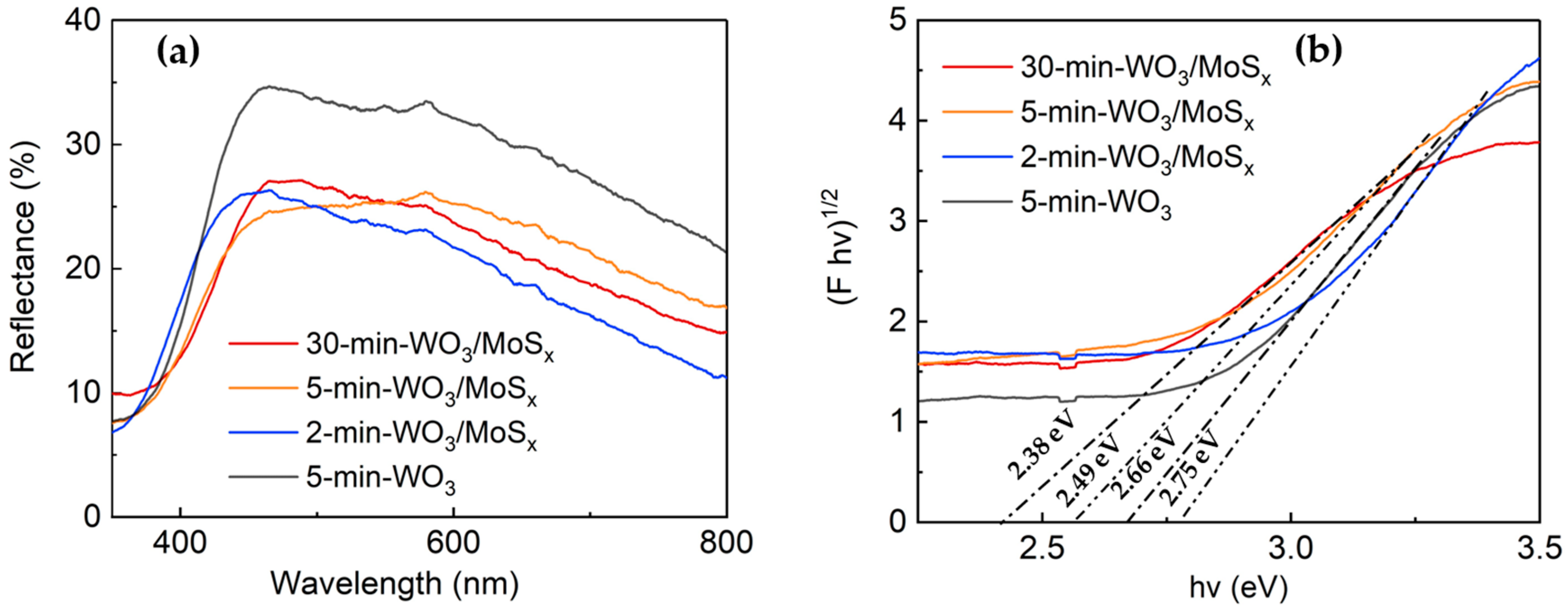
3.2.1. Optical Properties

The optical properties of the heterostructured and WO3 films were measured by UV-visible light spectroscopy. Figure 6a shows the diffuse reflectance spectra obtained at wavelengths in the range of 300 to 800 nm. As expected, the absorption maximum for all films lies in the UVA range at ~360 nm. Moreover, the heterostructures have evidently decreased reflectance in comparison to 5-min-WO3 film, which attests to the changes in the structure of the obtained novel materials. Furthermore, an increase in the synthesis time resulted in a red shift of the absorption edge. These films also have a fairly prominent absorption tail in the visible light region. It has been proposed that for WO3-based materials, visible light absorption can be attributed to surface W5+ sites [59,60]; however, in this study, XPS showed almost no W5+ for 5-min-WO3/MoSx. Thus, visible light absorption may be an effect of compositing with MoSx, or perhaps the existence of W5+ sites deeper within the film cavities into which XPS cannot penetrate. The band gaps also depend on synthesis conditions and have a clear tendency to decrease with increased synthesis time (Figure 6b). In particular, 2.75 eV, 2.49 eV, and 2.38 eV band gaps were calculated for the 2-min, 5-min, and 30 min films, respectively. The 5-min-WO3 has a larger band gap (2.66 eV) than the heterostructure counterpart, which indicates alteration of optical properties through incorporation of MoSx.

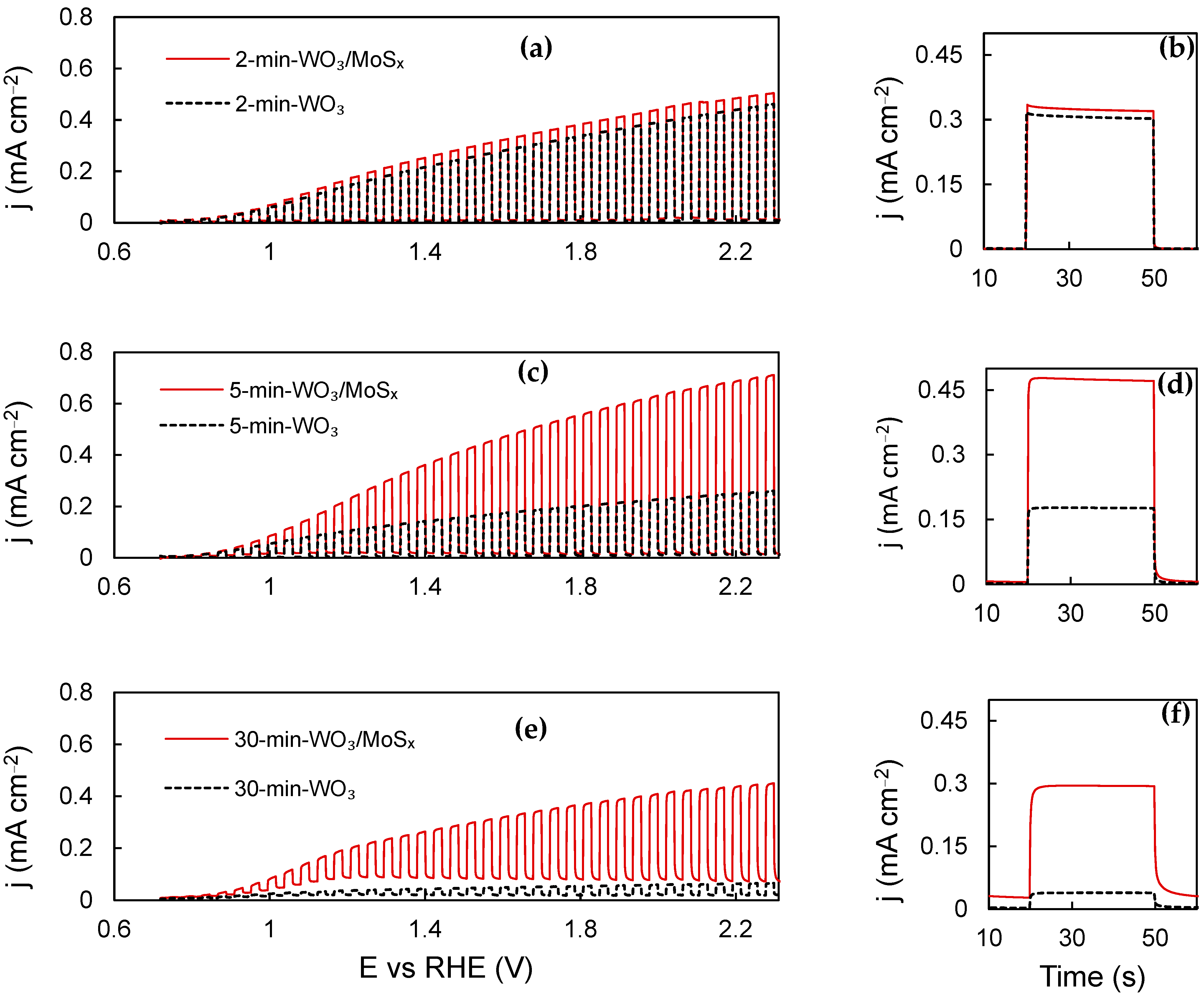
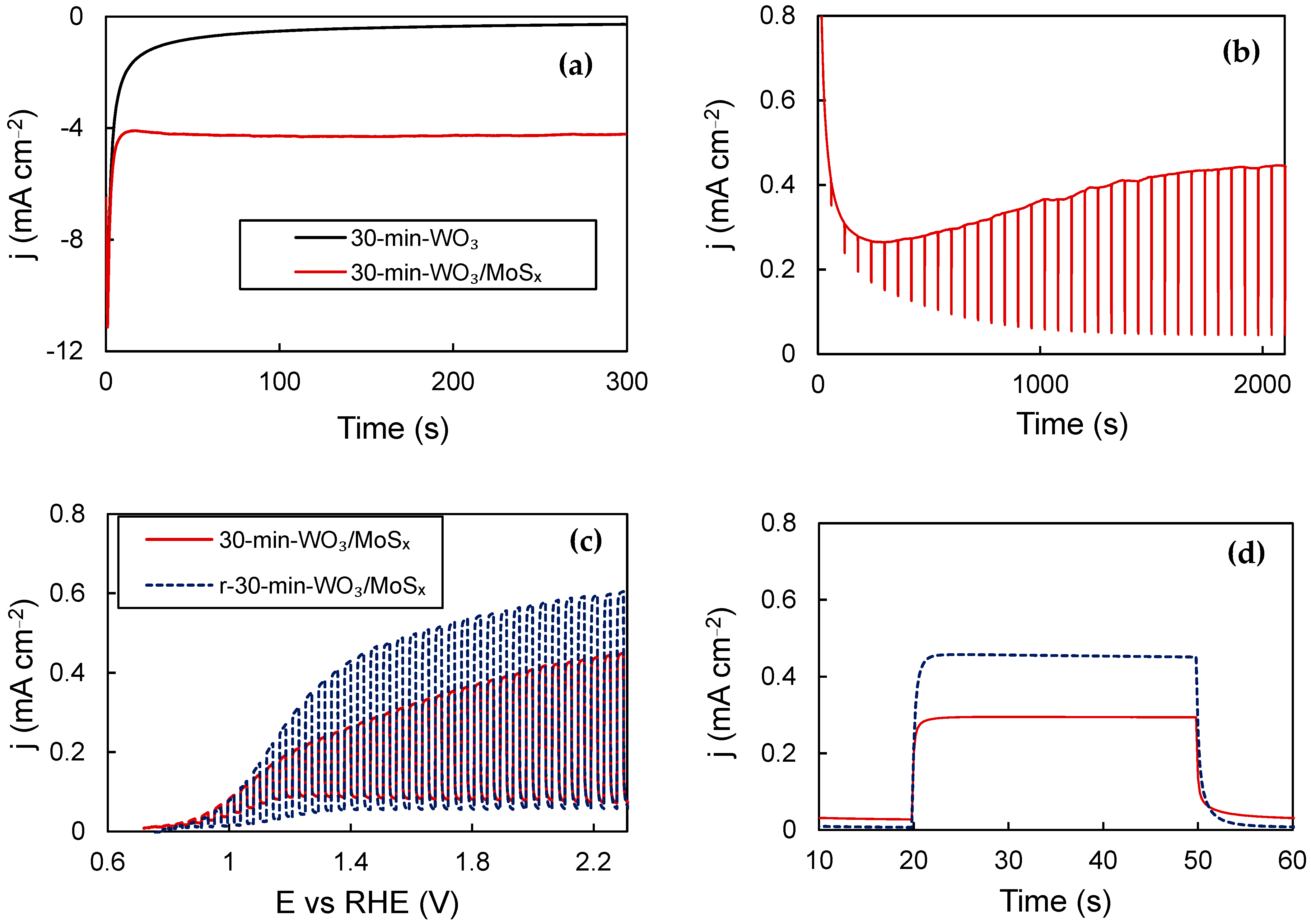
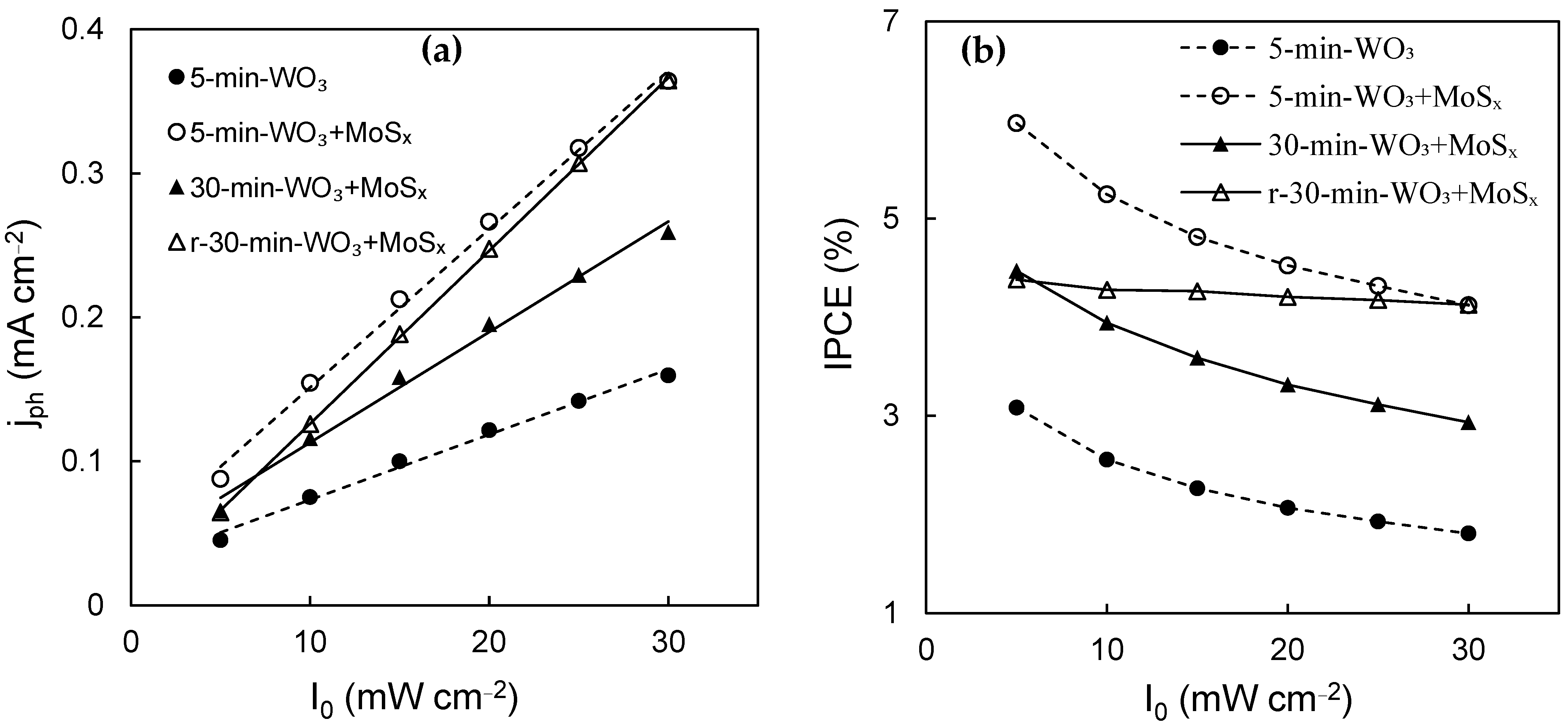
3.2.2. Photoelectrochemical Properties

The PEC activity curves obtained for WO3 and WO3/MoSx films are shown in Figure 7a,c,e. For all films, starting from onset at ~0.8 V, the photocurrent increases with applied potential, which is expected as the space–charge layer expands. The photocurrent of the films that had been synthesized for 2 min is relatively similar, which may be explained by recalling Figure 1 and the related discussion. During this shortest duration of synthesis, the same voltage is reached, regardless of the presence of MoS42− in the electrolyte. Consequently, very little MoSx is incorporated into the film. For the 5 min WO3 and WO3/MoSx films, an essential difference in their PEC properties is seen, illustrating the effect of incorporation of MoSx into WO3. The thickest films are unique; 30-min-WO3 has very poor PEC activity, whereas the heterostructure shows significantly higher activity. The 30-min-WO3/MoSx film has a strong anodic background current component that can be inferred from the “UV OFF” parts of the LSV curve. The origin of such current is electrochemical rather photoelectrochemical, and may be related to the charging current of a large surface area. However, anodic oxidation of the incorporated MoSx material is also possible.
Potentiostatic light pulse measurements were carried out in order to evaluate the steady-state photocurrent, and the data obtained at 1.53 V vs. RHE are presented in Figure 7b,d,f. The largest photocurrent is generated by the 5-min-WO3/MoSx sample is ~0.47 mA·cm−2, representing a 2.6-fold improvement over 0.17 mA·cm−2 for 5-min-WO3. Here, it is also important to examine the initial photocurrent (jt=0) versus the steady-state photocurrent, which is assumed as the stable current at the end of the 30 s pulse (jt=30) minus the background current (jph = jt=30 − jbg). If jt=0 is larger than jt=30, we know that recombination of photogenerated holes and electrons occurs at the electrode–electrolyte interface, and this limits the photoelectrochemical current. In this case, no significant recombination is seen. In addition, for the 30-min-WO3/MoSx, sample jt=0 is smaller than jt=30, which shows slower photogenerated charge transfer kinetics.
Previously, it was demonstrated that cathodic electrochemical reduction/H+ intercalation into WO3 films synthesized by the same method enhances their PEC properties [45]. This is also true for obtained WO3/MoSx heterostructures, and the biggest improvement in PEC properties was obtained for the thickest film (30-min-WO3/MoSx). The chronoamperometric curve registered during reduction shows that the current density settles at ~−4 mA·cm−2, compared to ‒0.3 mA·cm−2 for a plain WO3 film (Figure 8a). Then, a potential of 1.53 V was applied and the electrode was illuminated, with 2 s OFF pauses every 60 s. (Figure 8b). The photocurrent, which is the difference between the dark current and total current, plateaus after ~2000 s. Then, the PEC characterization was repeated, and it is evident that the reduced film (r-30-min-WO3/MoSx) exhibits superior performance to the entire measured potential range (Figure 8c) and in steady-state pulse measurements (Figure 8d), estimated to be an increase of ~30%. This improvement can be attributed to the same process that had been characterized with XPS before, i.e., the reduction of W6+ to W5+ by intercalated protons, followed by oxygen vacancy restructuring towards more optimal levels during activation [45].
In order to establish a more comprehensive characterization of the PEC properties of these materials, the photocurrent response was evaluated in relation to the light intensity (I0). According to the simplified Gärtner–Butler equation [61], the current generated by a photoanode will be a function of two variables: the width of the space charge layer and incident photon flux. The former is related to applied/bias potential and is reflected by potential sweep experiments, whereas the incident photon flux is directly proportional to I0. As can be inferred from the Gärtner–Butler equation, provided charge carrier photogeneration and transfer is the rate-limiting step, then jph~I0.
It is indeed observed that for all measured photoanodes that the photocurrent grows linearly from 5 mW·cm−2 to 30 mW·cm−2 for all films (Figure 9a). The unmodified WO3 film generates the lowest photocurrents, which is also proven by results presented in Figure 7, whereas the heterostructures show improved PEC activity at all light intensities. IPCE, on the other hand, is inversely related to I0, which means that photon conversion efficiency drops with increasing light intensity. This trend is observed for the measured photoanodes (Figure 9b), wherein the largest IPCE values are calculated at 5 mW·cm−2, and the lowest at 30 mW·cm−2. The best photon conversion efficiency at 1.53 V was obtained for the 5-min-WO3/MoSx film, at 6%. It is also evident that after reduction, the r-30-min-WO3/MoSx photoanode’s PEC properties improved significantly. The decrease in IPCE with I0 is not as sharp for this film, which is a contrasting characteristic in comparison to the non-reduced films, in which IPCE drops with I0 at a similar rate. The cause of this behavior is uncertain, but in practical terms, it means that higher light intensities can be used with fewer potential photon conversion efficiency losses.

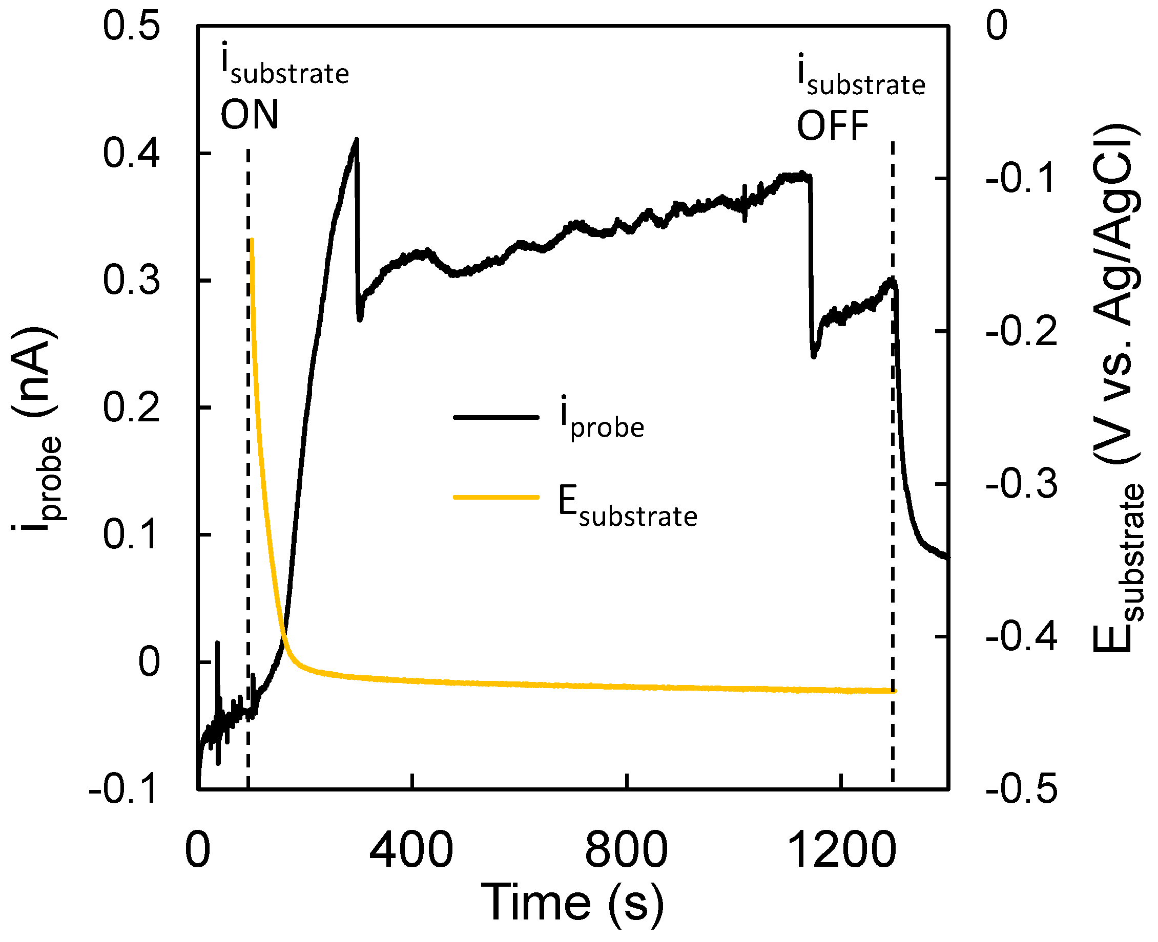
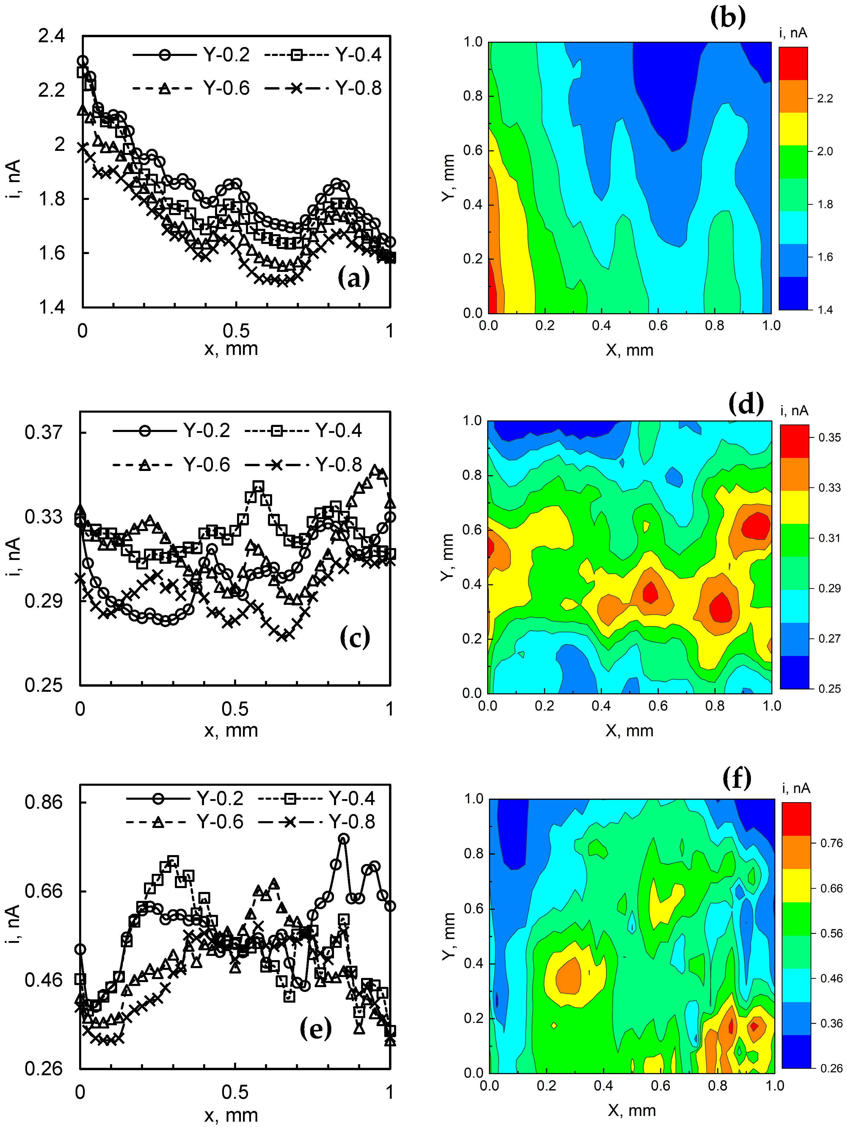
3.2.3. Scanning Electrochemical Microscopy of HER

Electrochemically deposited MoS2 is typically an excellent HER catalyst in acidic media. MoS2-x can be electrodeposited either cathodically or anodically (see Equation (7)). However, during PEO, MoSx is incorporated into the oxide film through plasma discharges, as discussed in Section 3.1. XPS has already shown that stoichiometric MoS2 exists on the surface of the heterostructured films. It was therefore decided to characterize their local and total HER electrocatalytic properties.
Due to the random nature of plasma discharges in PEO, MoSx should not coat the anode surface evenly. Previous experience has shown that scanning electrochemical microscopy (SECM) can be used to measure the local hydrogen evolution activity of MoS2 on complex surface structures [62]. The substrate generation–tip collection (SG-TC) mode is used, wherein the substrate generates hydrogen by the Heyrovsky step (Equation (8)) and the probe oxidizes it (Equation (9)):
M H + H 3 O + + e H 2 + H 2 O + M
H 2 2 H + + 2 e
It was determined that mild galvanostatic conditions are ideal for substrate generation. At −0.3 mA·cm−2, the substrate emits a constant signal, and little gaseous hydrogen is produced. Because at cathodic potentials, WO3/MoSx not only generates H2 but also intercalates H+, the substrates were initially subjected to simple equilibration conditioning at −0.3 mA·cm−2 for 1200 s.
Additionally, it was important to relate the current measured by the probe to the signal produced by the substrate. To accomplish this, the probe current (iprobe) was recorded for 100 s with the substrate at OCP (Figure 10). After 100 s, a current of −0.3 mA was applied on the WO3/MoSx substrate, as previously, which caused the potential of the substrate to drop and settle at ~−0.42 V vs. sat Ag/AgCl within 120 s. During this time, iprobe rose rapidly to ~0.4 nA, which confirms that the probe does indeed react to the signal produced by the substrate. It must also be noted that iprobe is not particularly stable. Several sharp drops are seen, which were most likely caused by the accumulation of gaseous H2 to form bubbles and block the probe. However, these conditions were considered optimal for 2D mapping, and it was presumed that as the probe is mobile during a scan bubble, accumulation would be less likely.
The SECM mapping data are shown in Figure 11, which consists of 2D slices, as well as 2D and maps of the respective film. For 2-min-WO3/MoSx, no particularly features could be distinguished (Figure 11a–c). As expected from SEM and FIB observations, this seems to be the smoothest film in terms of surface roughnessand it contains the smallest amount of MoSx. Even so, in the 2D profile, small bumps of current are observed at ~0.4–0.5 mm and 0.7 to 0.9 mm, but due to their linear continuity across the Y axis, these are more likely substrate topography-related signals. More interestingly, HER electrocatalytic activity maps are obtained for 5-min-WO3/MoSx (Figure 11d–f). In this case, significant inhomogeneity of HER activity is observed in the 1 × 1 mm map. Several islands of increased local activity emerge and occupy an area of ~0.2 × 0.2 mm. The 2D slices also show a more random distribution of HER activity compared to the previous film. This result certainly shows that areas of increased local HER activity exist on the surface of a WO3/MoSx heterostructure, but this may be related both to the presence of MoSx as well as to the surface topography. Similar results were obtained for the 30-min-WO3/MoSx film (Figure 11g,h,j), showing comparable dimension spots of increased electrocatalytic activity on the surface. In this case, however, the difference between the smallest and largest measured currents is ~0.5 nA (for the 5-min-WO3/MoSx film it was 0.1 nA). If these results are cross-referenced with SEM and FIB observations, it may be inferred that this film, due to its larger roughness and MoSx content, also has more inhomogeneity in local HER activity.

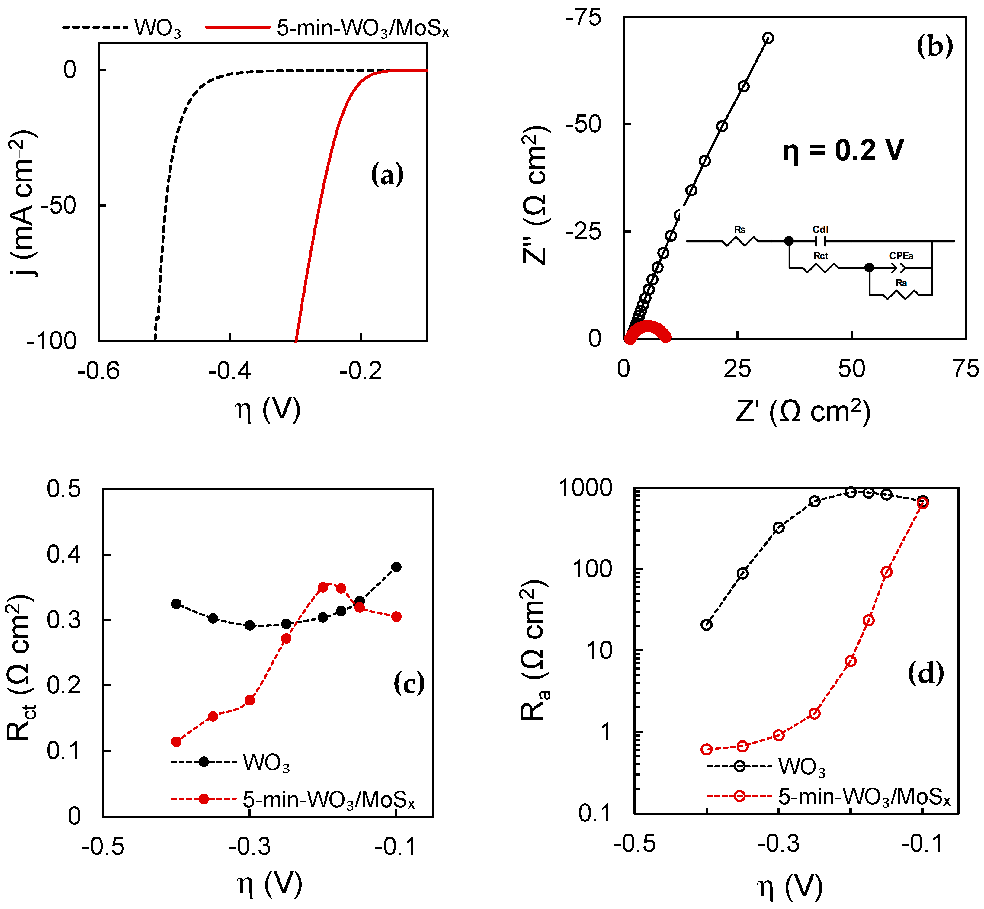
3.2.4. Total HER Activity

The HER electrocatalytic properties were also evaluated in terms of total electrode activity. The LSV curves shown in Figure 12a are corrected for iR-drop by the values of uncompensated resistance (often relating only to the resistance of the solution) obtained by means of EIS. These curves are typical of hydrogen’s evolution in acidic media. All plain WO3 films showed identical HER activity regardless of synthesis duration. The same is also true of the heterostructures, except for the 2-min-WO3/MoSx film, which could be expected due to its comparatively low MoSx content. Therefore, a comparison is drawn between a characteristic WO3 and a 5-min-WO3/MoSx film. The WO3 film has an η10mA (overpotential at which 10 mA·cm−2 HER current is reached) of −0.45 V, and a Tafel slope of 74.1 mA·dec−1. The comparable WO3/MoSx exhibits significantly better electrocatalytic activity, having a η10mA of −0.22 V and a Tafel slope of 42.6 mV·dec−1. Both parameters are ~2 times better in terms of efficiency in comparison to the respective WO3 films, and are typical of MoS2-based materials in acidic media [25].
In addition, EIS was used to characterize the catalyst–solution interface at increasing overpotentials. When comparing WO3 and heterostructured films at the same overpotential, it is apparent that the impedance of the WO3/MoSx film is smaller (Figure 12b) because the rate of HER is higher. Here, the spectrum in the Nyquist coordinates is represented by a low-frequency semicircle, which is related to the rate-limiting hydrogen adsorption process for HER on MoS2 under such conditions [24].
By fitting the obtained impedance spectra to an equivalent electric circuit (EEC), the values of the discrete capacitive and resistive features of the catalyst–solution interface can be calculated. The used circuit is shown in the inset of Figure 12b, where Rs is the uncompensated resistance (solution resistance), Cdl is the double layer capacitance, Rct is the charge transfer resistance, CPEa is the constant phase element that models hydrogen adsorption related capacitance, and Ra is the hydrogen adsorption resistance.
This model comprises two RC components: the high frequency component (Cdl-Rct) that is related to the Heyrovsky electrochemical recombination step, and the low frequency component (CPEa-Ra) that simulates the slower Volmer hydrogen adsorption step. The resistance parameters are inversely related to the rate of their corresponding electrochemical reactions, and therefore their relation to the applied overpotential gives information on the kinetics of the hydrogen evolution reaction. For both WO3 and WO3/MoSx, Rct values (Figure 12c) are similar in the overpotential range, where little HER occurs (−0.1 V to ~−0.2 V). However, for WO3/MoSx, Rct drops sharply from ~−0.2 V, coinciding with the onset of vigorous HER. At −0.4 V, Rct approaches the lowest value of 0.11 Ω cm2. The WO3 film does not exhibit this behavior because the HER current density at −0.4 V was only approximately 1.5 mA·cm−2. Moreover, Cdl is caused by the charge/discharge of the double layer at the catalyst–solution interface, and is therefore proportional to the electrochemically active surface area (ECSA). It was found that Cdl values obtained at −0.1 V for the 2-min, 5 min and 30 min films were 0.73 mF·cm−2, 1.06 mF·cm−2 and 1.53 mF·cm−2, respectively, showing that longer synthesis durations resulted in a larger ECSA. The same ratio was retained at each applied overpotential. For comparison, Cdl of the 5-min-WO3 film was 1.17 mF·cm−2, which shows that the non-heterostructured film has a slightly larger electrochemically active surface area.
The hydrogen adsorption resistance Ra is even more closely linked to the HER activity of the catalysts. Because the rate of HER is limited by the Volmer hydrogen adsorption step, the measured current density and overall reaction rate are determined by the low-frequency adsorption-related parameters, especially Ra. The adsorption resistance decreases with increasingly negative overpotentials because H+ is more readily adsorbed (Figure 12d). However, it is apparent that on the heterostructured material, Ra drops more swiftly until ~−0.3 V and then plateaus. For WO3, in contrast, Ra continues to decrease at −0.4 V. Experiments showed that at large enough overpotentials, the Ra values become equal, but for the heterostructure, lower Ra values are reached at lower overpotentials, which is expected of a heterogeneous HER electrocatalyst.

4. Conclusions

In this work, a bifunctional catalyst based on WO3 and MoS2 was prepared by relatively low-current plasma electrolytic oxidation of W in an electrolyte containing a MoS42− precursor. SEM observations revealed a rough surface morphology comprising disordered pores of up to 500 nm diameter, depending on synthesis time. Film thickness was also directly related to the duration of synthesis, and ranged from 0.56 µm to 3.5 µm. The presence of non-stoichiometric MoSx was confirmed by EDX and observed by elemental mapping only for the thickest film. XPS measurements showed a relatively strong Mo4+-S signal, suggesting that stoichiometric MoS2 also exists in the film. Although the films were not annealed, due to the nature of PEO, they exhibited a degree of crystallinity, and the WO3 was found to be monoclinic. The band gap ranged from 2.38 eV to 2.75 eV, depending on the duration of synthesis. This crystallinity and the incorporation of a lower band gap material (MoS2) means that even the as-deposited films performed as rather efficient photoanodes for photoelectrochemical water splitting, and could reach an IPCE of ~6%. The effect of electrochemical reduction was also discussed and used to further improve the PEC activity. Due to the presence of MoSx these materials can also act as HER electrocatalysts, and this was confirmed by measuring their HER activity in 0.5 M H2SO4. The best obtained Tafel slope (42.6 mV·dec−1) can be compared to that of electrocatalytic MoS2 films. Electrochemical impedance spectroscopy confirmed that the improved electrocatalytic HER activity is due to enhanced H+ adsorption, which is attributed to MoS2. Scanning electrochemical microscopy was used to evaluate the local HER activity of the heterostructured films. It was found that differences in local activity can be discerned on a millimeter-level and could be related to the synthesis duration of the respective films (and thus to morphology and composition). Overall, the WO3/MoSx heterostructures combine the best photo/electrochemical properties of WO3 and MoS2 into one versatile smart material.

Author Contributions

Conceptualization, R.L., N.T. and H.C.; methodology, R.L. and N.T.; formal analysis, R.L.; investigation, R.L., R.V. and K.G.; resources, H.C., R.V., L.T.-T. and E.N.; writing—original draft preparation, R.L.; writing—review and editing, R.L., N.T., H.C., L.T.-T. and E.N.; visualization, R.L., R.V. and K.G.; supervision, H.C. and E.N.; project administration, H.C.; funding acquisition, H.C. All authors have read and agreed to the published version of the manuscript.

Funding

This research has received funding from the European Union’s Horizon 2020 research and innovation program under the Marie Sklodowska-Curie grant agreement, No. 778357-SMARTELECTRODES. It has been performed in cooperation with the Research Council of Lithuania (LMTLT), agreement No. S-PD-22-5—TICAL, and partially with National Agency for Research and Development, Moldova, project No. 20.80009.5007.18.

Institutional Review Board Statement

Not applicable.

Informed Consent Statement

Not applicable.

Data Availability Statement

Data sharing is not applicable to this article.

Conflicts of Interest

The authors declare no conflict of interest.

References

  1. Xu, S.; Carter, E.A. Theoretical Insights into Heterogeneous (Photo)Electrochemical CO2 Reduction. Chem. Rev. 2019, 119, 6631–6669. [Google Scholar] [CrossRef] [PubMed]
  2. Gopinath, M.; Marimuthu, R. A Review on Solar Energy-Based Indirect Water-Splitting Methods for Hydrogen Generation. Int. J. Hydrogen Energy 2022, 47, 37742–37759. [Google Scholar] [CrossRef]
  3. Møller, K.T.; Jensen, T.R.; Akiba, E.; Li, H. Hydrogen—A Sustainable Energy Carrier. Prog. Nat. Sci. Mater. Int. 2017, 27, 34–40. [Google Scholar] [CrossRef]
  4. Wappler, M.; Unguder, D.; Lu, X.; Ohlmeyer, H.; Teschke, H.; Lueke, W. Building the Green Hydrogen Market—Current State and Outlook on Green Hydrogen Demand and Electrolyzer Manufacturing. Int. J. Hydrogen Energy 2022, 47, 33551–33570. [Google Scholar] [CrossRef]
  5. Razi, F.; Dincer, I. A Critical Evaluation of Potential Routes of Solar Hydrogen Production for Sustainable Development. J. Clean. Prod. 2020, 264, 121582. [Google Scholar] [CrossRef]
  6. Morales, W.; Cason, M.; Aina, O.; de Tacconi, N.R.; Rajeshwar, K. Combustion Synthesis and Characterization of Nanocrystalline WO3. J. Am. Chem. Soc. 2008, 130, 6318–6319. [Google Scholar] [CrossRef]
  7. Widiyandari, H.; Firdaus, I.; Kadarisman, V.G.S.; Purwanto, A. Optical Properties and Photocatalytic Activities of Tungsten Oxide (WO3) with Platinum Co-Catalyst Addition. In AIP Conference Proceedings; AIP Publishing LLC: Jatinangor, Indonesia, 2016; p. 050027. [Google Scholar]
  8. Bharagav, U.; Ramesh Reddy, N.; Nava Koteswara Rao, V.; Ravi, P.; Sathish, M.; Rangappa, D.; Prathap, K.; Shilpa Chakra, C.; Shankar, M.V.; Appels, L.; et al. Bifunctional G-C3N4/Carbon Nanotubes/WO3 Ternary Nanohybrids for Photocatalytic Energy and Environmental Applications. Chemosphere 2023, 311, 137030. [Google Scholar] [CrossRef] [PubMed]
  9. Knöppel, J.; Kormányos, A.; Mayerhöfer, B.; Hofer, A.; Bierling, M.; Bachmann, J.; Thiele, S.; Cherevko, S. Photocorrosion of WO3 Photoanodes in Different Electrolytes. ACS Phys. Chem. Au 2021, 1, 6–13. [Google Scholar] [CrossRef] [PubMed]
  10. Bai, S.; Zhang, K.; Luo, R.; Li, D.; Chen, A.; Liu, C.C. Low-Temperature Hydrothermal Synthesis of WO3 Nanorods and Their Sensing Properties for NO2. J. Mater. Chem. 2012, 22, 12643. [Google Scholar] [CrossRef]
  11. Tehrani, F.S.; Ahmadian, H.; Aliannezhadi, M. Hydrothermal Synthesis and Characterization of WO3 Nanostructures: Effect of Reaction Time. Mater. Res. Express 2020, 7, 015911. [Google Scholar] [CrossRef]
  12. Judeinstein, P.; Livage, J. Sol–Gel Synthesis of WO3 Thin Films. J. Mater. Chem. 1991, 1, 621–627. [Google Scholar] [CrossRef]
  13. Mohamedkhair, A.K.; Drmosh, Q.A.; Qamar, M.; Yamani, Z.H. Tuning Structural Properties of WO3 Thin Films for Photoelectrocatalytic Water Oxidation. Catalysts 2021, 11, 381. [Google Scholar] [CrossRef]
  14. Sadale, S.B.; Chaqour, S.M.; Gorochov, O.; Neumann-Spallart, M. Photoelectrochemical and Physical Properties of Tungsten Trioxide Films Obtained by Aerosol Pyrolysis. Mater. Res. Bull. 2008, 43, 1472–1479. [Google Scholar] [CrossRef]
  15. Brada, M.; Neumann-Spallart, M.; Krýsa, J. Tungsten Trioxide Film Photoanodes Prepared by Aerosol Pyrolysis for Photoelectrochemical Applications. Catal. Today 2022, 413–415, 113981. [Google Scholar] [CrossRef]
  16. Poongodi, S.; Kumar, P.S.; Mangalaraj, D.; Ponpandian, N.; Meena, P.; Masuda, Y.; Lee, C. Electrodeposition of WO3 Nanostructured Thin Films for Electrochromic and H2S Gas Sensor Applications. J. Alloys Compd. 2017, 719, 71–81. [Google Scholar] [CrossRef]
  17. Mineo, G.; Ruffino, F.; Mirabella, S.; Bruno, E. Investigation of WO3 Electrodeposition Leading to Nanostructured Thin Films. Nanomaterials 2020, 10, 1493. [Google Scholar] [CrossRef]
  18. Coelho, D.; Gaudêncio, J.P.R.S.; Carminati, S.A.; Ribeiro, F.W.P.; Nogueira, A.F.; Mascaro, L.H. Bi Electrodeposition on WO3 Photoanode to Improve the Photoactivity of the WO3/BiVO4 Heterostructure to Water Splitting. Chem. Eng. J. 2020, 399, 125836. [Google Scholar] [CrossRef]
  19. Levinas, R.; Tsyntsaru, N.; Lelis, M.; Cesiulis, H. Synthesis, Electrochemical Impedance Spectroscopy Study and Photoelectrochemical Behaviour of as-Deposited and Annealed WO3 Films. Electrochim. Acta 2017, 225, 29–38. [Google Scholar] [CrossRef]
  20. Fernández-Domene, R.M.; Roselló-Márquez, G.; Sánchez-Tovar, R.; Cifre-Herrando, M.; García-Antón, J. Synthesis of WO3 Nanorods through Anodization in the Presence of Citric Acid: Formation Mechanism, Properties and Photoelectrocatalytic Performance. Surf. Coat. Technol. 2021, 422, 127489. [Google Scholar] [CrossRef]
  21. Yeh, C.-W.; Wu, K.-R.; Hung, C.-H.; Chang, H.-C.; Hsu, C.-J. Preparation of Porous F-WO3/TiO2 Films with Visible-Light Photocatalytic Activity by Microarc Oxidation. Int. J. Photoenergy 2012, 2012, 285129. [Google Scholar] [CrossRef] [Green Version]
  22. Stojadinović, S.; Radić, N.; Vasilić, R.; Petković, M.; Stefanov, P.; Zeković, L.; Grbić, B. Photocatalytic Properties of TiO2/WO3 Coatings Formed by Plasma Electrolytic Oxidation of Titanium in 12-Tungstosilicic Acid. Appl. Catal. B Environ. 2012, 126, 334–341. [Google Scholar] [CrossRef]
  23. Bayati, M.R.; Golestani-Fard, F.; Moshfegh, A.Z.; Molaei, R. A Photocatalytic Approach in Micro Arc Oxidation of WO3–TiO2 Nano Porous Semiconductors under Pulse Current. Mater. Chem. Phys. 2011, 128, 427–432. [Google Scholar] [CrossRef]
  24. Meng, C.; Chen, X.; Gao, Y.; Zhao, Q.; Kong, D.; Lin, M.; Chen, X.; Li, Y.; Zhou, Y. Recent Modification Strategies of MoS2 for Enhanced Electrocatalytic Hydrogen Evolution. Molecules 2020, 25, 1136. [Google Scholar] [CrossRef] [PubMed] [Green Version]
  25. Benck, J.D.; Hellstern, T.R.; Kibsgaard, J.; Chakthranont, P.; Jaramillo, T.F. Catalyzing the Hydrogen Evolution Reaction (HER) with Molybdenum Sulfide Nanomaterials. ACS Catal. 2014, 4, 3957–3971. [Google Scholar] [CrossRef]
  26. Seo, B.; Joo, S.H. Recent Advances in Unveiling Active Sites in Molybdenum Sulfide-Based Electrocatalysts for the Hydrogen Evolution Reaction. Nano Converg. 2017, 4, 19. [Google Scholar] [CrossRef] [PubMed] [Green Version]
  27. Tang, Q.; Jiang, D. Stabilization and Band-Gap Tuning of the 1T-MoS2 Monolayer by Covalent Functionalization. Chem. Mater. 2015, 27, 3743–3748. [Google Scholar] [CrossRef] [Green Version]
  28. Zhu, Y.; Song, L.; Song, N.; Li, M.; Wang, C.; Lu, X. Bifunctional and Efficient CoS2–C@MoS2 Core–Shell Nanofiber Electrocatalyst for Water Splitting. ACS Sustain. Chem. Eng. 2019, 7, 2899–2905. [Google Scholar] [CrossRef]
  29. Ali, S.A.; Ahmad, T. Chemical Strategies in Molybdenum Based Chalcogenides Nanostructures for Photocatalysis. Int. J. Hydrogen Energy 2022, 47, 29255–29283. [Google Scholar] [CrossRef]
  30. Zhou, D.; Shu, H.; Hu, C.; Jiang, L.; Liang, P.; Chen, X. Unveiling the Growth Mechanism of MoS2 with Chemical Vapor Deposition: From Two-Dimensional Planar Nucleation to Self-Seeding Nucleation. Cryst. Growth Des. 2018, 18, 1012–1019. [Google Scholar] [CrossRef]
  31. Cho, Y.J.; Sim, Y.; Lee, J.-H.; Hoang, N.T.; Seong, M.-J. Size and Shape Control of CVD-Grown Monolayer MoS2. Curr. Appl. Phys. 2023, 45, 99–104. [Google Scholar] [CrossRef]
  32. Yue, J.; Jian, J.; Dong, P.; Luo, L.; Chang, F. Growth of Single-Layer MoS2 by Chemical Vapor Deposition on Sapphire Substrate. IOP Conf. Ser. Mater. Sci. Eng. 2019, 592, 012044. [Google Scholar] [CrossRef]
  33. Vattikuti, S.V.P.; Byon, C.; Reddy, C.V. Synthesis of MoS2 Multi-Wall Nanotubes Using Wet Chemical Method with H2O2 as Growth Promoter. Superlattices Microstruct. 2015, 85, 124–132. [Google Scholar] [CrossRef]
  34. Wojtalik, M.; Bojarska, Z.; Makowski, Ł. Experimental Studies on the Chemical Wet Synthesis for Obtaining High-Quality MoS2 Nanoparticles Using Impinging Jet Reactor. J. Solid State Chem. 2020, 285, 121254. [Google Scholar] [CrossRef]
  35. Falola, B.D.; Wiltowski, T.; Suni, I.I. Electrodeposition of MoS2 for Charge Storage in Electrochemical Supercapacitors. J. Electrochem. Soc. 2016, 163, D568–D574. [Google Scholar] [CrossRef] [Green Version]
  36. Levinas, R.; Tsyntsaru, N.; Cesiulis, H. Insights into Electrodeposition and Catalytic Activity of MoS2 for Hydrogen Evolution Reaction Electrocatalysis. Electrochim. Acta 2019, 317, 427–436. [Google Scholar] [CrossRef]
  37. Noori, Y.J.; Thomas, S.; Ramadan, S.; Smith, D.E.; Greenacre, V.K.; Abdelazim, N.; Han, Y.; Beanland, R.; Hector, A.L.; Klein, N.; et al. Large-Area Electrodeposition of Few-Layer MoS2 on Graphene for 2D Material Heterostructures. ACS Appl. Mater. Interfaces 2020, 12, 49786–49794. [Google Scholar] [CrossRef]
  38. Vizza, M.; Giurlani, W.; Cerri, L.; Calisi, N.; Leonardi, A.A.; Faro, M.J.L.; Irrera, A.; Berretti, E.; Perales-Rondón, J.V.; Colina, A.; et al. Electrodeposition of Molybdenum Disulfide (MoS2) Nanoparticles on Monocrystalline Silicon. Molecules 2022, 27, 5416. [Google Scholar] [CrossRef]
  39. Rakibuddin, M.; Kim, H. Fabrication of MoS2 /WO3 Nanocomposite Films for Enhanced Electro-Chromic Performance. New J. Chem. 2017, 41, 15327–15333. [Google Scholar] [CrossRef]
  40. Singh, S.; Sharma, S. Ammonia Sensing Using MoS2/WO3 Composite Obtained via Top-down Approach. Mater. Today Proc. 2021, 43, 137–140. [Google Scholar] [CrossRef]
  41. Shahid, W.; Idrees, F.; Iqbal, M.A.; Tariq, M.U.; Shahid, S.; Choi, J.R. Ex Situ Synthesis and Characterizations of MoS2/WO3 Heterostructures for Efficient Photocatalytic Degradation of RhB. Nanomaterials 2022, 12, 2974. [Google Scholar] [CrossRef]
  42. Simchen, F.; Sieber, M.; Kopp, A.; Lampke, T. Introduction to Plasma Electrolytic Oxidation—An Overview of the Process and Applications. Coatings 2020, 10, 628. [Google Scholar] [CrossRef]
  43. Sikdar, S.; Menezes, P.V.; Maccione, R.; Jacob, T.; Menezes, P.L. Plasma Electrolytic Oxidation (PEO) Process—Processing, Properties, and Applications. Nanomaterials 2021, 11, 1375. [Google Scholar] [CrossRef] [PubMed]
  44. Levinas, R.; Tsyntsaru, N.; Cesiulis, H. The Characterisation of Electrodeposited MoS2 Thin Films on a Foam-Based Electrode for Hydrogen Evolution. Catalysts 2020, 10, 1182. [Google Scholar] [CrossRef]
  45. Levinas, R.; Tsyntsaru, N.; Murauskas, T.; Cesiulis, H. Improved Photocatalytic Water Splitting Activity of Highly Porous WO3 Photoanodes by Electrochemical H+ Intercalation. Front. Chem. Eng. 2021, 3, 760700. [Google Scholar] [CrossRef]
  46. Mortazavi, G.; Jiang, J.; Meletis, E.I. Investigation of the Plasma Electrolytic Oxidation Mechanism of Titanium. Appl. Surf. Sci. 2019, 488, 370–382. [Google Scholar] [CrossRef]
  47. Venkateswarlu, K.; Rameshbabu, N.; Sreekanth, D.; Sandhyarani, M.; Bose, A.C.; Muthupandi, V.; Subramanian, S. Role of Electrolyte Chemistry on Electronic and in Vitro Electrochemical Properties of Micro-Arc Oxidized Titania Films on Cp Ti. Electrochim. Acta 2013, 105, 468–480. [Google Scholar] [CrossRef]
  48. Qi, H.; Wolfe, J.; Wang, D.; Fan, H.J.; Fichou, D.; Chen, Z. Triple-Layered Nanostructured WO3 Photoanodes with Enhanced Photocurrent Generation and Superior Stability for Photoelectrochemical Solar Energy Conversion. Nanoscale 2014, 6, 13457–13462. [Google Scholar] [CrossRef]
  49. Polunin, A.V.; Cheretaeva, A.O.; Borgardt, E.D.; Rastegaev, I.A.; Krishtal, M.M.; Katsman, A.V.; Yasnikov, I.S. Improvement of Oxide Layers Formed by Plasma Electrolytic Oxidation on Cast Al Si Alloy by Incorporating TiC Nanoparticles. Surf. Coat. Technol. 2021, 423, 127603. [Google Scholar] [CrossRef]
  50. Bhattacharya, R.N.; Lee, C.Y.; Pollak, F.H.; Schleich, D.M. Optical Study of Amorphous MoS3: Determination of the Fundamental Energy Gap. J. Non-Cryst. Solids 1987, 91, 235–242. [Google Scholar] [CrossRef]
  51. Laperriere, G.; Marsan, B.; Belanger, D. Preparation and Characterization of Electrodeposited Amorphous Molybdenum Sulfide. Synth. Met. 1989, 29, 201–206. [Google Scholar] [CrossRef]
  52. Bélanger, D.; Laperriére, G.; Marsan, B. The Electrodeposition of Amorphous Molybdenum Sulfide. J. Electroanal. Chem. 1993, 347, 165–183. [Google Scholar] [CrossRef]
  53. Ismail, S.; Ng, C.Y.; Ahmadi, E.; Razak, K.A.; Lockman, Z. Segmented Nanoporous WO3 Prepared via Anodization and Their Photocatalytic Properties. J. Mater. Res. 2016, 31, 721–728. [Google Scholar] [CrossRef]
  54. Chen, J.; Xia, Y.; Yang, J.; Chen, B. Fabrication of Monolayer MoS2/RGO Hybrids with Excellent Tribological Performances through a Surfactant-Assisted Hydrothermal Route. Appl. Phys. A 2018, 124, 430. [Google Scholar] [CrossRef]
  55. Li, Y.; Nakamura, R. Structural Change of Molybdenum Sulfide Facilitates the Electrocatalytic Hydrogen Evolution Reaction at Neutral PH as Revealed by in Situ Raman Spectroscopy. Chin. J. Catal. 2018, 39, 401–406. [Google Scholar] [CrossRef]
  56. Kibsgaard, J.; Jaramillo, T.F.; Besenbacher, F. Building an Appropriate Active-Site Motif into a Hydrogen-Evolution Catalyst with Thiomolybdate [Mo3S13]2− Clusters. Nat. Chem 2014, 6, 248–253. [Google Scholar] [CrossRef] [PubMed] [Green Version]
  57. Tran, P.D.; Tran, T.V.; Orio, M.; Torelli, S.; Truong, Q.D.; Nayuki, K.; Sasaki, Y.; Chiam, S.Y.; Yi, R.; Honma, I.; et al. Coordination Polymer Structure and Revisited Hydrogen Evolution Catalytic Mechanism for Amorphous Molybdenum Sulfide. Nat. Mater 2016, 15, 640–646. [Google Scholar] [CrossRef]
  58. Merki, D.; Fierro, S.; Vrubel, H.; Hu, X. Amorphous Molybdenum Sulfide Films as Catalysts for Electrochemical Hydrogen Production in Water. Chem. Sci. 2011, 2, 1262–1267. [Google Scholar] [CrossRef] [Green Version]
  59. Abe, R.; Takami, H.; Murakami, N.; Ohtani, B. Pristine Simple Oxides as Visible Light Driven Photocatalysts: Highly Efficient Decomposition of Organic Compounds over Platinum-Loaded Tungsten Oxide. J. Am. Chem. Soc. 2008, 130, 7780–7781. [Google Scholar] [CrossRef]
  60. Boruah, P.J.; Khanikar, R.R.; Bailung, H. Synthesis and Characterization of Oxygen Vacancy Induced Narrow Bandgap Tungsten Oxide (WO3−x) Nanoparticles by Plasma Discharge in Liquid and Its Photocatalytic Activity. Plasma Chem Plasma Process 2020, 40, 1019–1036. [Google Scholar] [CrossRef]
  61. Hankin, A.; Bedoya-Lora, F.E.; Alexander, J.C.; Regoutz, A.; Kelsall, G.H. Flat Band Potential Determination: Avoiding the Pitfalls. J. Mater. Chem. A 2019, 7, 26162–26176. [Google Scholar] [CrossRef] [Green Version]
  62. Levinas, R.; Grigucevičienė, A.; Kubilius, T.; Matijošius, A.; Tamašauskaitė-Tamašiūnaitė, L.; Cesiulis, H.; Norkus, E. Femtosecond Laser-Ablated Copper Surface as a Substrate for a MoS2-Based Hydrogen Evolution Reaction Electrocatalyst. Materials 2022, 15, 3926. [Google Scholar] [CrossRef] [PubMed]
Figure 1. Voltage vs. time plots obtained for PEO of W at 25 mA cm−2 during synthesis of WO3 and WO3/MoSx heterostructures in the respective electrolytes.
Coatings 13 00673 g001
Figure 2. SEM surface morphology and FIB cross-sectional morphology of WO3/MoSx heterostructures, obtained after synthesis for 2 min (a,d), 5 min (b,e), 30 min (c,f).
Coatings 13 00673 g002
Figure 3. XRD diffractograms of W substrate, a WO3 film synthesized for 5 min, and heterostructured films, synthesized for 2, 5, and 30 min.
Coatings 13 00673 g003
Figure 4. EDX elemental composition maps of 30-min-WO3/MoSx heterostructured coating. Cross-sectional view (a), and top-down view (b).
Coatings 13 00673 g004
Figure 5. High-resolution XPS spectra of a 5-min-WO3/MoSx film: Mo3d (a), S2p (b), W4f (c).
Coatings 13 00673 g005aCoatings 13 00673 g005b
Figure 6. Diffuse reflectance spectra (a) and Tauc plots with band gap calculations (b) of WO3/MoSx and 5-min-WO3 films.
Coatings 13 00673 g006
Figure 7. Chopped-UV LSV curves (a,c,e) and steady-state photocurrent pulses, measured at 1.53 V (b,d,f). See Table 1 for more details.
Coatings 13 00673 g007
Figure 8. Chronoamperometric curves for WO3/MoSx and WO3 reduction at −0.28 V (a); activation curve of reduced 30-min-WO3/MoSx (b); chopped-UV LSV curves (c); steady-state photocurrent pulses (d). See Table 1 for more details.
Coatings 13 00673 g008
Figure 9. Values of photocurrents generated by WO3, WO3/MoSx, and reduced WO3/MoSx films at 1.53 V and under different light intensities (a); IPCE (%) values calculated from photocurrents (b).
Coatings 13 00673 g009
Figure 10. Trends of substrate potential and probe current over time. Obtained in 0.5 M H2SO4. Substrate, 5-min-WO3/MoSx; tip, 25 µm diameter Pt microelectrode.
Coatings 13 00673 g010
Figure 11. 2D profiles and 2D SECM maps: 2-min-WO3/MoSx (a,b); 5-min-WO3/MoSx (c,d); 30-min-WO3/MoSx (e,f) films, obtained in 0.5 M H2SO4. Probe scan speed 100 µm s−1, data acquisition at 25 µm intervals with a 25 µm diameter probe.
Coatings 13 00673 g011
Figure 12. HER characterization data of WO3 and heterostructured films: LSV scans at 2 mV s−1 corrected by iR-drop (a); EIS spectra obtained at overpotential −0.2 V in complex plane coordinates, where solid lines show equivalent circuit fits (inset shows equivalent circuit used to fit spectra) (b); values of Rct as a function of overpotential (c); values of Ra as a function of overpotential (d).
Coatings 13 00673 g012
Table 1. Outline of experiments used to characterize the PEC and HER properties of synthesized catalysts. Potentials were recalculated vs. RHE.
StepPEC (0.1 M Na2SO4, pH 2)HER (0.5 M H2SO4)
1Settling of OCP for 60 s.Settling of OCP for 60 s.
2LSV scan from 0.72 V to 2.3 V
at 2 mV·s−1, with 10 s ON/OFF pulses
of 25 mW·cm−2 365 nm light.
LSV at 2 mV·s−1 from 0 V to a cut-off current density −100 mA·cm−2.
3Potentiostatic illumination pulse at 1.53 V.EIS measurements from −0.1 V
to −0.5 V. Spectra obtained
from 10 kHz to 100 mHz,
perturbation amplitude ±10 mV.
4Electrochemical reductive treatment
of 30-min-WO3/MoSx
Fitting data with Zview software.
5Repeat of steps 1–3 for r-30-min-WO3/MoSx
Disclaimer/Publisher’s Note: The statements, opinions and data contained in all publications are solely those of the individual author(s) and contributor(s) and not of MDPI and/or the editor(s). MDPI and/or the editor(s) disclaim responsibility for any injury to people or property resulting from any ideas, methods, instructions or products referred to in the content.

