Article

Combined HF+MW CVD Approach for the Growth of Polycrystalline Diamond Films with Reduced Bow

1
Prokhorov General Physics Institute of the Russian Academy of Sciences, 38 Vavilov Str., Moscow 119991, Russia
2
Kotel’nikov Institute of Radio Engineering and Electronics, Russian Academy of Sciences, 1 Vvedensky Sq., Fryazino 141190, Russia
3
Tomsk Polytechnic University, 30 Lenin Ave., Tomsk 634050, Russia
4
Institute for Advanced Materials and Technology, University of Science and Technology Beijing, Beijing 100083, China
5
MIREA—Russian Technological University, 78 Vernadsky Ave., Moscow 119454, Russia
*
Author to whom correspondence should be addressed.
Coatings 2023, 13(2), 380; https://doi.org/10.3390/coatings13020380
Submission received: 31 December 2022 / Revised: 3 February 2023 / Accepted: 6 February 2023 / Published: 7 February 2023
(This article belongs to the Special Issue 2D Materials-Based Thin Films and Coatings)

Abstract

:
A combination of two methods of chemical vapor deposition (CVD) of diamond films, microwave plasma–assisted (MW CVD) and hot filament (HF CVD), was used for the growth of 100 µm-thick polycrystalline diamond (PCD) layers on Si substrates. The bow of HF CVD and MW CVD films showed opposite convex\concave trends; thus, the combined material allowed reducing the overall bow by a factor of 2–3. Using MW CVD for the growth of the initial 25 µm-thick PCD layer allowed achieving much higher thermal conductivity of the combined 110 µm-thick film at 210 W/m·K in comparison to 130 W/m·K for the 93 µm-thick pure HF CVD film.

1. Introduction

Among all known materials, diamond has a record-high thermal conductivity of up to 24 W/cm·K at room temperature, reaching maximum values of up to 285 W/cm·K at temperatures near 63 K. [1] This makes diamond the material of the choice for various thermal management applications [2,3,4,5,6,7]. The possibility of the organization of an effective heat transfer from the active zones in modern electronic devices makes diamond the “cutting-edge” material in electronics. [8,9,10,11]. In the last years, great attention in the “Power Electronics” field has been directed towards gallium nitride (GaN) devices, as their high electric field strength and electron mobility have already shown tremendous potential for high-frequency communications and photonic applications [12,13,14]. However, the low thermal conductivity (TC) of only 2 W/cm·K at room temperature limits the use of GaN devices in high-performance regimes [13]. Thus, the great prospect of combining GaN devices with diamond thermal management layers may be achieved by the means of layer bonding or the direct growth of diamond layers on GaN heterostructures [14,15,16,17].
Although single-crystal diamond is preferred for effective heat sinks, it remains a high-priced material, with principal limitations on the size of high-quality crystals that are well below the standards for the electronic industry [18,19,20]. So, much more inexpensive and potentially wider-sized polycrystalline diamond (PCD) films and plates are usually used instead [21,22,23,24,25]. Such material is composed of smaller 10–100 μm-sized diamond grains, which still have a negative effect on the thermal conductivity of PCD material in comparison with single-crystal material [26,27]. Still, the TC values of thick high-quality PCD plates reach 20–22 W/cm·K at room temperature [23,28,29], which is quite close to the TC of single crystals and, in general, satisfies the requirements for high-end heat sinks.
The highest-quality CVD diamond is grown in microwave plasma (MW CVD) in standard methane–hydrogen gas mixtures [30,31] with the potential of adding other gases for diamond doping [32,33] or the formation of diamond-based composites [34,35,36]. The absence of heated electrodes (as sources of impurities) with a combination of the possibility to minimize the non-diamond sp2 phase in the grown material allows the formation of high-TC PCD films. However, the plasma size and, consequently, substrate dimension, are principally limited by the frequency of the microwave generator. For the most common 2.45 GHz CVD reactors, the largest substrate size for stable growth is ≈2 inches [31,37], while attempts to use larger 3–4 inch plates usually result in the reduction of uniformity of the grown films. Even more complicated 915 MHz CVD reactors or novel DC-arc Jet CVD systems [38] allow an increase in the size of PCD plates up to 4–6 inches [23] but at the price of decreased cost efficiency and increased complexity of the process.
Another CVD technique uses hot filaments (HF CVD) to activate methane and hydrogen precursors for diamond growth [39,40]. This method has no principal limitation on the size and number of samples for the growth of PCD layers, which makes it a much more cost-effective technology in comparison to MW CVD. However, in this case, the obtained material is unavoidably contaminated with the material of filaments (usually tungsten), resulting in reduced thermal conductivity [41]. This limits the use of HF CVD diamond films predominantly to hard or protective coatings, e.g., for cutting tools [40,42,43].
The CVD growth of PCD films follows the van der Drift competitive model [44]. Diamond grains start as nanometer-sized nuclei and increase in size in the course of CVD growth. The initial layer of PCD film that is grown at the very beginning of the CVD process has the smallest size of diamond grains [45,46], which drastically decreases the TC of this layer due to the scattering of phonons on the grain boundaries [47]. For this reason, the initial PCD layer is usually removed by polishing or etching in order to achieve higher TC values of PCD plates [23,48], a procedure that obviously cannot be performed in the case of diamond films not separated from the substrate. Thus, more sophisticated techniques should be used to increase the TC of such PCD coatings.
In this work, we present a new approach for the efficient formation of PCD layers on Si substrates by a consecutive combination of MW CVD (2.45 GHz reactor) and HF CVD growth. The higher-quality MW CVD material is used for the TC-critical initial layer of PCD film, while later, a more cost-effective HF CVD growth is used. The structure, phase composition, bow, and the resulting TC of the combined MW+HF CVD sample are compared to separate MW CVD and HF CVD samples with similar thicknesses.

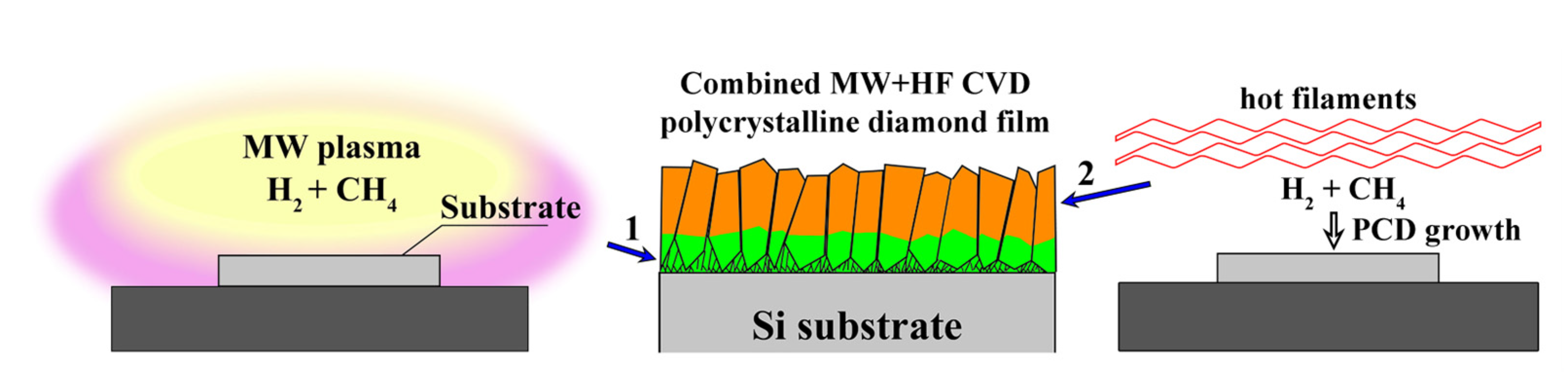
2. Materials and Methods

The overall scheme of the experiment is shown in Figure 1. The combination of MW CVD and HF CVD techniques is used for the growth of 100 µm-thick PCD layers on the Si substrates.
The initial substrates were 19 × 19 × 0.5 mm3 Si plates that were laser-cut from a single (111)-oriented plate with a diameter of 100 mm. The exact choice of size and the orientation of substrates was motivated by suitability for the formation of GaN-on-Diamond structures by the method shown in our previous work [14]. Substrates were seeded with nanodiamond particles (≈5 nm) from water-based suspension using ultrasound treatment for 10 min and drying in air.
MW CVD diamond films were synthesized by microwave plasma CVD reactor ARDIS-100 (2.45 GHz, Optosystems Ltd., Moscow, Russia) in CH4/H2 gas mixtures [21,31] with a constant total gas flow rate of 500 sccm, methane concentration of 3%, pressure of 55 Torr, and microwave power of 4.8 kW. The substrate temperature was measured through a top window with a Micron M770 two-beam pyrometer (Mikron Infrared Inc., Santa Clara, CA, USA) and was kept at 850 ± 25 °C. The growth rate was ≈1 µm per hour, which allowed us to obtain high-quality PCD films. After the CVD process, the final thickness of the PCD film was controlled by the mass gain of each sample. Two samples were grown in separate runs: the “MW CVD” sample on Si (film thickness ≈112 µm) and a similar sample with the thickness of PCD layer of only 25 µm, which was later used as a substrate for HF CVD growth. To avoid contamination influencing the combined growth, no investigations of the 25 µm-thick MW CVD sublayer were performed.
For HF CVD diamond deposition, a laboratory-built HF reactor with tungsten filaments (d = 0.16 mm) was used. During the experiments, methane concentration in the H2 (99.999%)/CH4 (99.99%) gas mixture was maintained at 6 vol.%. To keep the substrate temperature even at T = 850 ± 20 °C, and thus obtain uniform diamond coating, the distance between tungsten filaments and substrates was set as 12 ± 1 mm. The average current per filament was 6 ± 0.1 A. The operating pressure was maintained at 20 ± 1 Torr throughout the synthesis using a needle valve. The average film growth rate was about 1.1 µm/h. Here, we note, that exact HF CVD conditions were purposely aimed at the high growth rates and not at maximizing the quality of the films. The filaments were not changed during the entire deposition process. Two samples were grown in the same run: the “HF CVD” sample on a seeded Si substrate and the “MW+HF CVD” sample on a previously grown MW CVD 25µm-thick PCD layer on Si. Thus, to prepare the bi-layer film (MW+HF sample), the first layer was grown on Si in the MW CVD system, and then the sample was transferred into the HF CVD system. In both cases, the thickness of the grown HF CVD layers was ≈95 µm.
To minimize the influence of edge effects, which is typical for all types of CVD growth (e.g., see [49]), 1 mm wide strips were laser-cut from each side of each sample, including the HFCVD-grown one, so their final size was 17 × 17 mm2.
The phase composition of the obtained films was analyzed at room temperature with micro-Raman spectroscopy using the LABRAM HR-800 spectrometer (Horiba Ltd., Tokyo, Japan) equipped with a diode-pumped solid-state laser (λ = 473 nm). The spectrometer operated in a confocal mode, while the laser beam was focused in a spot of ≈1 μm in diameter of the sample surface. The film surface morphology was examined with scanning electron microscopy (SEM) using the instrument Tescan MIRA3 (TESCAN, Brno, Czech Republic). The curvature and surface roughness of the resulting “diamond-on-Si” plates were measured with an optical profilometer, NewView 5000 (ZYGO Corp., Middlefield, CT, USA). Specifically, the bow of each sample was measured from the bottom (Si substrate) side and was used to calculate the radius of curvature. The surface profiles of the CVD-grown films were taken over a 360 × 255 μm area in the central part of each PCD surface, and the exact surface roughness values (Rrms, or Sq as in ISO 25178) were calculated by the in-built software of the instrument.
The thermal conductivity of the PCD sample was measured with a laser flash technique (LFT) method [50,51] on a laboratory-built setup. Specifically, the diffusivity D⟂ in the direction perpendicular to the sample surface was determined. A pulsed YAG:Nd laser (wavelength 1.06 µm, pulse width 8 ns) was used for sample surface heating, while the temperature kinetics were monitored with a HgCdTe detector. Before the measurement, the Si substrate was removed by the means of wet etching in an HNO3-HF acid mixture, the 4 × 10 mm PCD sample was cut from the central part of the PCD plate with a CO2 laser, and then thin Ti layers (≈400 nm) were deposited on both sides of the sample to enhance the laser absorption and IR emissivity. The thermal conductivity was found according to the relation k = DρC, where ρ and C are the density and the temperature-dependent specific heat of diamond, respectively.

3. Results and Discussion

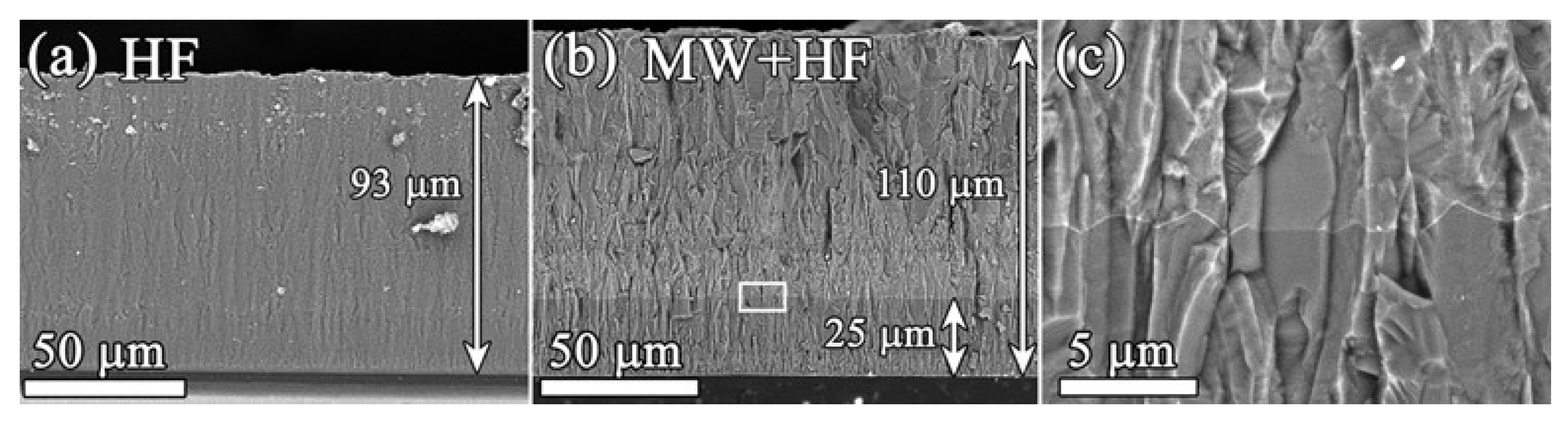
3.1. SEM Characterization

Figure 2 demonstrates comparative cross-sectional SEM images of the HF CVD sample and the combined MW+HF CVD sample. Pure HF CVD shows a rather uniform columnar structure of the grains throughout the whole PCD film, with a thickness of 93 µm. Surprisingly, in the combined MW+HF CVD sample, the exact interface between the HF and MW parts of the sample is clearly visible in the “backscattered electrons” (BSE) mode of the microscope. Thus, we can reliably measure the thickness of the MW CVD layer at 25 µm, while the thickness of an additional HF CVD layer was 85 µm (full thickness 110 µm). So, in the MW+HF CVD sample, the ratio between MW and HF phases is “1 to 3.4” strongly in favor of the HF CVD material.
Plan-view SEM images of MW CVD, HF CVD, and MW+HF CVD samples are demonstrated in Figure 3. The MW CVD sample consists of well-faceted diamond grains with sizes of 10–40 µm, which is evidence of the high quality of PCD film. The average grain size for the bottom 25 µm-thick MW CVD layer was ≈10 µm, as deduced from corresponding SEM images (not shown here). The HF CVD sample is composed of much smaller poorly-faceted 5–20 µm grains, with occasional inclusions of nanocrystalline diamond phase due to secondary nucleation processes and twinning of diamond grains. The combination of MW and HF CVD techniques led to the structure of the film similar to the MW CVD material, with predominantly large crystallites, although grains smaller than 5 µm, which were formed due to secondary nucleation, were also observed. Considering the fact that the majority of the PCD layer was grown in the HF CVD regime, this underlines the critical effect of the initial CVD layer on the structure of the whole PCD film.

3.2. Raman Spectroscopy

The phase composition of all grown PCD films was studied with Raman spectroscopy (Figure 4). The spectrum of all films shows an intensive diamond first-order Raman peak near 1333 cm−1 with a full width at half maximum (FWHM) Δν ≈ 8 cm−1. The bottom 25 µm MW CVD layer exhibits the Raman peak broadened to Δν = 9.2 cm−1, which is typical for finer grain films with an enhanced content of defects and grain boundaries, while for thick (112 µm) MW CVD, the peak width decreases to Δν = 6.8 cm−1. For all films, the exact positions of Raman peaks are slightly shifted from their original position at 1332.5 cm−1, which is evidence of the stress in the film [52]. Such stress is a combination of (a) thermal stress, generated in the process of cooling the sample from the temperature of CVD synthesis (850 °C) down to room temperature due to the difference in thermal expansion coefficients (TEC) of diamond and silicon; and (b) intrinsic stress caused by formed defects and the polycrystalline nature of the film. In the case of CVD growth of PCD layers on thin substrates, such stress usually results in the notable bow of the “diamond-on-Si” plates [53,54]. The reduction of such thermal stress and related plate curvature is one of the main goals for the optimization of the CVD growth process. Notably, HF CVD and MW CVD have opposite trends of the resulting stress, which is slightly tensile for HF CVD material and slightly compressive for MW CVD one. The stress of the combined material is even highly compressive, which might be caused by the additional stress at the MW→HF interface (see Figure 2c).
Another feature of the Raman spectra is the peak at 1490 cm−1 is evidence of trans-polyacetylene (t-PA) in the grain boundaries [55]. This peak is the most intense for the HF CVD material and nearly absent for the MW CVD sample and, in general, inversely correlates with the size of the diamond grains, as seen in Figure 3.

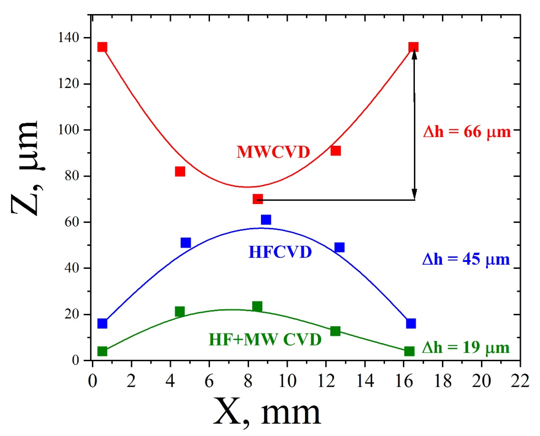
3.3. Bow of the PCD-Si Samples

The bow (Δh), the radius of curvature (r), and the surface roughness of PCD film (Rrms) of each sample were measured from the bottom (substrate) side using the white light interferometry technique (Figure 5). The radius of curvature r was calculated from the Δh values as a more universal parameter, as for larger-diameter substrates, higher Δh values are expected. For the bi-layer film, the curvature radius increases to 1.9 m (Table 1). For initial Si substrates, the bow was measured at ≈0.8 μm. The measured bow values for PCD-Si samples were: Δh(HF) = −45 μm; Δh(HF+MW) = −19 μm; Δh(MW) = 66 μm. Note that the bow for HF CVD and MW CVD samples have opposite positive/negative bow trends (see similar trends for different MW/HF samples, e.g., in works [21,54]). The bow of the combined MW+HF CVD sample was the lowest and closer to the HF CVD sample, as the majority of the combined PCD film was grown by HF CVD.

3.4. Roughness and Thermal Conductivity

The results of the experiments are summarized in Table 1. The growth of the bottom PCD layer by MW CVD allowed increasing the TC of the combined MW+HF CVD film by ≈60% to k = 210 W/m·K, to decrease its bow by 57%, and to decrease the roughness by ≈45% in comparison to the pure HF CVD sample with k = 130 W/m·K. The PCD films produced by MW CVD typically possess a better structural quality and better purity compared to those for HF CVD films. The best PCD films with a thickness of a few hundred microns (and with large grain size) produced by MW CVD have TC as high as 2000–2200 W/m·K [23,28,29]. In contrast, HFCVD PCD shows lower TC [56], typically less than 1200 W/m·K [41]. Our TC data (Table 1) confirm the superiority of the MW CVD diamond samples. The present results on the bow and thermal conductivity of MW CVD films are compatible with those reported by us earlier for 2-inch MW CVD PCD films on Si [21].
Our estimates of the independent TC value for the 25 μm-thick MW CVD layer in MW+HF film show that the measured improvement in TC for the combined sample cannot be achieved at any value of conductivity of the MW sub-layer if the TC of the 85 µm-thick HF top film will be the same as for the single-layer HF sample with a close thickness of 93 µm. Therefore, the TC of the HF top film itself was also improved due to a combination of using higher-quality material in the critical initial part of PCD film and the increased grain size of diamond grains. Thus, the role of the primary relatively thin MW layer is both to increase the TC of the bottom part of the composite film and provide a larger grain size for the next HF film (Figure 3). The root-mean-squared surface roughness Rrms of 1.9 for composite films turns out lower than that for the single-layer MW CVD and HF CVD films (2.2 and 2.7 μm, respectively). The roughness improvement for the bilayer was due to a better overall homogeneity in the thickness for MW+HF PCD film at the scale of hundreds of micrometers.

4. Conclusions

The consecutive combination of MW CVD and HF CVD growth of 110 μm-thick PCD layer on Si substrate was performed. Its structure, phase composition, bow, and thermal conductivity were compared with ones for samples grown purely in MW CVD and HF CVD conditions, accordingly. It was shown that using MW CVD for the growth of the initial 25 μm of the PCD layer allowed increasing the grain size and the TC of the resulting film by ≈60% while decreasing the bow by 57% in comparison to the 93 μm-thick HF CVD sample.
The potential of the demonstrated approach lies not only in the field of thermal management applications of PCD films but is also applicable for improving the quality of HF CVD-grown films in general. In the future, other combinations of different types of CVD growth of diamond could be interesting for investigation as well. As the HF CVD technique allows deposition on substrates of large size, the multiple substrates with pre-grown MW CVD layers may be used at the same time for increased cost efficiency. Moreover, the 2-inch limit of MW CVD reactors working at 2.45 GHz can be surpassed by using 915 MHz CVD reactors or DC-arc Jet CVD systems.
The bow is reduced here owing to the compensation of thermal stress (compressive) by intrinsic stress (tensile). In principle, the intrinsic stress in MW CVD diamond film can be tuned by methane content in gas or by substrate temperature. In addition, the stress is sensitive to nitrogen impurity content in the reactor and substrate holder shape. Therefore, the overall low bow can be obtained by growing the film in the same CVD system but changing the process regime at a certain moment of the growth run. The optimum film can be a bilayer (sharp change) and a gradient structure. This new research field may influence and improve the quality and cost-efficiency of CVD-grown diamond for various applications, such as thermal management and protective coatings for electronics, photonics, biomedicine, cutting tools, etc.

Author Contributions

Conceptualization, V.S. and J.W.; methodology, V.S. and S.L.; software, V.S. and A.M.; validation, V.R., V.K. and J.W.; formal analysis, A.P.; investigation, A.M., S.S., E.Z., S.Z. and A.G.; resources, A.M.; data curation, A.M.; writing—original draft preparation, V.S., A.P., A.M., S.L. and J.W.; writing—review and editing, V.S. and C.L.; visualization, V.S.; supervision, V.R., V.K. and C.L.; project administration, V.S. and S.L.; funding acquisition, S.L. and C.L. All authors have read and agreed to the published version of the manuscript.

Funding

The work was supported by the grant of the Russian Science Foundation (project No. 21-79-10004) in part of HFCVD and by National Natural Science Foundation of China (No. 52172037).

Institutional Review Board Statement

Not applicable.

Informed Consent Statement

Not applicable.

Data Availability Statement

Not applicable.

Acknowledgments

The authors would like to thank Soumen Mandal (Cardiff University, UK) for the provision of aqueous suspensions of nanodiamonds.

Conflicts of Interest

The authors declare no conflict of interest.

References

  1. Inyushkin, A.V.; Taldenkov, A.N.; Ralchenko, V.G.; Bolshakov, A.P.; Koliadin, A.V.; Katrusha, A.N. Thermal Conductivity of High Purity Synthetic Single Crystal Diamonds. Phys. Rev. B 2018, 97, 144305. [Google Scholar] [CrossRef]
  2. Hou, G.-Y.; Shu, S.-L.; Feng, J.; Popp, A.; Schmidt, B.; Lu, H.-Y.; Wang, L.-J.; Tian, S.-C.; Tong, C.-Z.; Wang, L.-J. High Power (>27 W) Semiconductor Disk Laser Based on Pre-Metalized Diamond Heat-Spreader. IEEE Photonics J. 2019, 11, 1501908. [Google Scholar] [CrossRef]
  3. Li, X.; Wang, X.; Li, Y.; Liu, Y. Production and Heat Properties of an X-Ray Reflective Anode Based on a Diamond Heat Buffer Layer. Materials 2020, 13, 241. [Google Scholar] [CrossRef] [PubMed]
  4. Yang, Q.; Zhao, J.; Huang, Y.; Zhu, X.; Fu, W.; Li, C.; Miao, J. A Diamond Made Microchannel Heat Sink for High-Density Heat Flux Dissipation. Appl. Therm. Eng. 2019, 158, 113804. [Google Scholar] [CrossRef]
  5. Nosaeva, K.; Al-Sawaf, T.; John, W.; Stoppel, D.; Rudolph, M.; Schmückle, F.-J.; Janke, B.; Krüger, O.; Krozer, V.; Heinrich, W.; et al. Multifinger Indium Phosphide Double-Heterostructure Transistor Circuit Technology with Integrated Diamond Heat Sink Layer. IEEE Trans. Electron Devices 2016, 63, 1846–1852. [Google Scholar] [CrossRef]
  6. Karczemska, A.; Witkowski, D.; Ralchenko, V.; Bolshakov, A.; Sovyk, D.; Lysko, J.; Hassard, J. Diamond Microfluidic Devices Manufactured with the Replica Method. In Proceedings of the 2009 5th International Conference on Perspective Technologies and Methods in MEMS Design, Lviv, Ukraine, 22–24 April 2009; pp. 17–19. [Google Scholar]
  7. Zheng, Y.; Jia, Y.; Liu, J.; Wei, J.; Chen, L.; An, K.; Yan, X.; Zhang, X.; Ye, H.; Ouyang, X. Surface Etching Evolution of Mechanically Polished Single Crystal Diamond with Subsurface Cleavage in Microwave Hydrogen Plasma: Topography, State and Electrical Properties. Vacuum 2022, 199, 110932. [Google Scholar] [CrossRef]
  8. Alcantar-Peña, J.J.; de Obaldia, E.; Tirado, P.; Arellano-Jimenez, M.J.; Ortega Aguilar, J.E.; Veyan, J.F.; Yacaman, M.J.; Koudriavtsev, Y.; Auciello, O. Polycrystalline Diamond Films with Tailored Micro/Nanostructure/Doping for New Large Area Film-Based Diamond Electronics. Diam. Relat. Mater. 2019, 91, 261–271. [Google Scholar] [CrossRef]
  9. Shikata, S. Single Crystal Diamond Wafers for High Power Electronics. Diam. Relat. Mater. 2016, 65, 168–175. [Google Scholar] [CrossRef]
  10. Jagannadham, K. Multilayer Diamond Heat Spreaders for Electronic Power Devices. Solid-State Electron. 1998, 42, 2199–2208. [Google Scholar] [CrossRef]
  11. Tadjer, M.J.; Anderson, T.J.; Hobart, K.D.; Feygelson, T.I.; Caldwell, J.D.; Eddy, C.R.; Kub, F.J.; Butler, J.E.; Pate, B.; Melngailis, J. Reduced Self-Heating in AlGaN/GaN HEMTs Using Nanocrystalline Diamond Heat-Spreading Films. IEEE Electron Device Lett. 2012, 33, 23–25. [Google Scholar] [CrossRef]
  12. Amano, H.; Baines, Y.; Beam, E.; Borga, M.; Bouchet, T.; Chalker, P.R.; Charles, M.; Chen, K.J.; Chowdhury, N.; Chu, R.; et al. The 2018 GaN Power Electronics Roadmap. J. Phys. D: Appl. Phys. 2018, 51, 163001. [Google Scholar] [CrossRef]
  13. Qin, H.; Luan, X.; Feng, C.; Yang, D.; Zhang, G. Mechanical, Thermodynamic and Electronic Properties of Wurtzite and Zinc-Blende GaN Crystals. Materials 2017, 10, 1419. [Google Scholar] [CrossRef] [PubMed]
  14. Chernykh, M.Y.; Andreev, A.A.; Ezubchenko, I.S.; Chernykh, I.A.; Mayboroda, I.O.; Kolobkova, E.M.; Khrapovitskaya, Y.V.; Grishchenko, J.V.; Perminov, P.A.; Sedov, V.S.; et al. GaN-Based Heterostructures with CVD Diamond Heat Sinks: A New Fabrication Approach towards Efficient Electronic Devices. Appl. Mater. Today 2022, 26, 101338. [Google Scholar] [CrossRef]
  15. Zhou, Y.; Ramaneti, R.; Anaya, J.; Korneychuk, S.; Derluyn, J.; Sun, H.; Pomeroy, J.; Verbeeck, J.; Haenen, K.; Kuball, M. Thermal Characterization of Polycrystalline Diamond Thin Film Heat Spreaders Grown on GaN HEMTs. Appl. Phys. Lett. 2017, 111, 041901. [Google Scholar] [CrossRef]
  16. Mu, F.; He, R.; Suga, T. Room Temperature GaN-Diamond Bonding for High-Power GaN-on-Diamond Devices. Scr. Mater. 2018, 150, 148–151. [Google Scholar] [CrossRef]
  17. Ohki, T.; Yamada, A.; Minoura, Y.; Makiyama, K.; Kotani, J.; Ozaki, S.; Sato, M.; Okamoto, N.; Joshin, K.; Nakamura, N. An over 20-W/Mm S-Band InAlGaN/GaN HEMT with SiC/Diamond-Bonded Heat Spreader. IEEE Electron Device Lett. 2018, 40, 287–290. [Google Scholar] [CrossRef]
  18. Arnault, J.-C.; Saada, S.; Ralchenko, V. Chemical Vapor Deposition Single-Crystal Diamond: A Review. Phys. Status Solidi–Rapid Res. Lett. 2022, 16, 2100354. [Google Scholar] [CrossRef]
  19. Ralchenko, V.G.; Inyushkin, A.V.; Shu, G.; Dai, B.; Karateev, I.A.; Bolshakov, A.P.; Khomich, A.A.; Ashkinazi, E.E.; Zavedeev, E.V.; Han, J. Thermal Conductivity of Diamond Mosaic Crystals Grown by Chemical Vapor Deposition: Thermal Resistance of Junctions. Phys. Rev. Appl. 2021, 16, 014049. [Google Scholar] [CrossRef]
  20. Liu, N.; Sugawara, K.; Yoshitaka, N.; Yamada, H.; Takeuchi, D.; Akabane, Y.; Fujino, K.; Kawai, K.; Arima, K.; Yamamura, K. Damage-Free Highly Efficient Plasma-Assisted Polishing of a 20-Mm Square Large Mosaic Single Crystal Diamond Substrate. Sci. Rep. 2020, 10, 19432. [Google Scholar] [CrossRef]
  21. Sedov, V.; Martyanov, A.; Altakhov, A.; Popovich, A.; Shevchenko, M.; Savin, S.; Zavedeev, E.; Zanaveskin, M.; Sinogeykin, A.; Ralchenko, V.; et al. Effect of Substrate Holder Design on Stress and Uniformity of Large-Area Polycrystalline Diamond Films Grown by Microwave Plasma-Assisted CVD. Coatings 2020, 10, 939. [Google Scholar] [CrossRef]
  22. Liang, Y.; Zheng, Y.; Wei, J.; Jia, X.; Zhu, X.; An, K.; Liu, J.; Chen, L.; Li, C. Effect of Grain Boundary on Polycrystalline Diamond Polishing by High-Speed Dynamic Friction. Diam. Relat. Mater. 2021, 117, 108461. [Google Scholar] [CrossRef]
  23. Popovich, A.F.; Ralchenko, V.G.; Balla, V.K.; Mallik, A.K.; Khomich, A.A.; Bolshakov, A.P.; Sovyk, D.N.; Ashkinazi, E.E.; Yurov, V.Y. Growth of 4″ diameter Polycrystalline Diamond Wafers with High Thermal Conductivity by 915 MHz Microwave Plasma Chemical Vapor Deposition. Plasma Sci. Technol. 2017, 19, 035503. [Google Scholar] [CrossRef]
  24. Komlenok, M.S.; Dezhkina, M.A.; Sedov, V.S.; Klimenko, O.A.; Dyakov, S.A.; Gippius, N.A. Laser Ablated Nanocrystalline Diamond Membrane for Infrared Applications. Sensors 2022, 22, 829. [Google Scholar] [CrossRef] [PubMed]
  25. Komlenok, M.; Pashinin, V.; Sedov, V.; Konov, V. Femtosecond and Nanosecond Laser Polishing of Rough Polycrystalline Diamond. Laser Phys. 2022, 32, 084003. [Google Scholar] [CrossRef]
  26. Sood, A.; Cheaito, R.; Bai, T.; Kwon, H.; Wang, Y.; Li, C.; Yates, L.; Bougher, T.; Graham, S.; Asheghi, M. Direct Visualization of Thermal Conductivity Suppression Due to Enhanced Phonon Scattering near Individual Grain Boundaries. Nano Lett. 2018, 18, 3466–3472. [Google Scholar] [CrossRef]
  27. Anaya, J.; Bai, T.; Wang, Y.; Li, C.; Goorsky, M.; Bougher, T.L.; Yates, L.; Cheng, Z.; Graham, S.; Hobart, K.D.; et al. Simultaneous Determination of the Lattice Thermal Conductivity and Grain/Grain Thermal Resistance in Polycrystalline Diamond. Acta Mater. 2017, 139, 215–225. [Google Scholar] [CrossRef]
  28. Wort, C.J.H.; Sweeney, C.G.; Cooper, M.A.; Scarsbrook, G.A.; Sussmann, R.S. Thermal Properties of Bulk Polycrystalline CVD Diamond. Diam. Relat. Mater. 1994, 3, 1158–1167. [Google Scholar] [CrossRef]
  29. Hartmann, J.; Voigt, P.; Reichling, M. Measuring Local Thermal Conductivity in Polycrystalline Diamond with a High Resolution Photothermal Microscope. J. Appl. Phys. 1997, 81, 2966–2972. [Google Scholar] [CrossRef]
  30. Ralchenko, V.G.; Smolin, A.A.; Konov, V.I.; Sergeichev, K.F.; Sychov, I.A.; Vlasov, I.I.; Migulin, V.V.; Voronina, S.V.; Khomich, A.V. Large-Area Diamond Deposition by Microwave Plasma. Diam. Relat. Mater. 1997, 6, 417–421. [Google Scholar] [CrossRef]
  31. Sedov, V.S.; Martyanov, A.K.; Khomich, A.A.; Savin, S.S.; Zavedeev, E.V.; Ralchenko, V.G. Deposition of Diamond Films on Si by Microwave Plasma CVD in Varied CH4-H2 Mixtures: Reverse Nanocrystalline-to-Microcrystalline Structure Transition at Very High Methane Concentrations. Diam. Relat. Mater. 2020, 109, 108072. [Google Scholar] [CrossRef]
  32. Sedov, V.; Ralchenko, V.; Khomich, A.; Vlasov, I.; Vul, A.; Savin, S.; Goryachev, A.; Konov, V. Si-Doped Nano-and Microcrystalline Diamond Films with Controlled Bright Photoluminescence of Silicon-Vacancy Color Centers. Diam. Relat. Mater. 2015, 56, 23–28. [Google Scholar] [CrossRef]
  33. Sedov, V.; Martyanov, A.; Savin, S.; Bolshakov, A.; Bushuev, E.; Khomich, A.; Kudryavtsev, O.; Krivobok, V.; Nikolaev, S.; Ralchenko, V. Growth of Polycrystalline and Single-Crystal CVD Diamonds with Bright Photoluminescence of Ge-V Color Centers Using Germane GeH4 as the Dopant Source. Diam. Relat. Mater. 2018, 90, 47–53. [Google Scholar] [CrossRef]
  34. Sedov, V.S.; Martyanov, A.K.; Khomich, A.A.; Savin, S.S.; Voronov, V.V.; Khmelnitskiy, R.A.; Bolshakov, A.P.; Ralchenko, V.G. Co-Deposition of Diamond and β-SiC by Microwave Plasma CVD in H2-CH4-SiH4 Gas Mixtures. Diam. Relat. Mater. 2019, 98, 107520. [Google Scholar] [CrossRef]
  35. Popovich, A.; Martyanov, A.; Khomich, A.; Fedotov, P.; Savin, S.; Sedov, V.; Ralchenko, V. CVD Diamond-SiC Composite Films: Structure and Electrical Properties. Diam. Relat. Mater. 2022, 125, 108975. [Google Scholar] [CrossRef]
  36. Ralchenko, V.; Sedov, V.; Martyanov, A.; Voronov, V.; Savin, S.; Khomich, A.; Shevchenko, M.; Bolshakov, A. Diamond-Germanium Composite Films Grown by Microwave Plasma CVD. Carbon 2022, 190, 10–21. [Google Scholar] [CrossRef]
  37. Yoshikawa, T.; Herrling, D.; Meyer, F.; Burmeister, F.; Nebel, C.E.; Ambacher, O.; Lebedev, V. Influence of Substrate Holder Configurations on Bias Enhanced Nucleation Area for Diamond Heteroepitaxy: Toward Wafer-Scale Single-Crystalline Diamond Synthesis. J. Vac. Sci. Technol. B Nanotechnol. Microelectron. Mater. Process. Meas. Phenom. 2019, 37, 021207. [Google Scholar] [CrossRef]
  38. Huang, Y.; Chen, L.; Shao, S.; Huang, K.; An, K.; Zheng, Y.; Liu, J.; Wei, J.; Li, C. The 7-in. Freestanding Diamond Thermal Conductive Film Fabricated by DC Arc Plasma Jet CVD with Multi-Stage Magnetic Fields. Diam. Relat. Mater. 2022, 122, 108812. [Google Scholar] [CrossRef]
  39. Fuentes-Fernandez, E.M.A.; Alcantar-Peña, J.J.; Lee, G.; Boulom, A.; Phan, H.; Smith, B.; Nguyen, T.; Sahoo, S.; Ruiz-Zepeda, F.; Arellano-Jimenez, M.J.; et al. Synthesis and Characterization of Microcrystalline Diamond to Ultrananocrystalline Diamond Films via Hot Filament Chemical Vapor Deposition for Scaling to Large Area Applications. Thin Solid Film. 2016, 603, 62–68. [Google Scholar] [CrossRef]
  40. Linnik, S.A.; Gaydaychuk, A.V.; Okhotnikov, V.V. Improvement to the Adhesion of Polycrystalline Diamond Films on WC-Co Cemented Carbides through Ion Etching of Loosely Bound Growth Centers. Surf. Coat. Technol. 2018, 334, 227–232. [Google Scholar] [CrossRef]
  41. Baba, K.; Aikawa, Y.; Shohata, N. Thermal Conductivity of Diamond Films. J. Appl. Phys. 1991, 69, 7313–7315. [Google Scholar] [CrossRef]
  42. Wang, H.; Wang, C.; Wang, X.; Sun, F. Effects of Carbon Concentration and Gas Pressure with Hydrogen-Rich Gas Chemistry on Synthesis and Characterizations of HFCVD Diamond Films on WC-Co Substrates. Surf. Coat. Technol. 2021, 409, 126839. [Google Scholar] [CrossRef]
  43. Martins, R.L.; Damm, D.D.; Volu, R.M.; Pinheiro, R.A.; Rosa, F.M.; Trava-Airoldi, V.J.; De Vasconcelos, G.; Barquete, D.M.; Corat, E.J. Laser Cladding of Vanadium Carbide Interlayer for CVD Diamond Growth on Steel Substrate. Surf. Coat. Technol. 2021, 421, 127387. [Google Scholar] [CrossRef]
  44. Van der Drift, A. Evolutionary Selection, a Principle Governing Growth Orientation in Vapour-Deposited Layers. Philips. Res. Rep. 1967, 22, 267. [Google Scholar]
  45. Podgursky, V.; Bogatov, A.; Sedov, V.; Sildos, I.; Mere, A.; Viljus, M.; Buijnsters, J.G.; Ralchenko, V. Growth Dynamics of Nanocrystalline Diamond Films Produced by Microwave Plasma Enhanced Chemical Vapor Deposition in Methane/Hydrogen/Air Mixture: Scaling Analysis of Surface Morphology. Diam. Relat. Mater. 2015, 58, 172–179. [Google Scholar] [CrossRef]
  46. Podgursky, V.; Bogatov, A.; Yashin, M.; Viljus, M.; Bolshakov, A.P.; Sedov, V.; Volobujeva, O.; Mere, A.; Raadik, T.; Ralchenko, V. A Comparative Study of the Growth Dynamics and Tribological Properties of Nanocrystalline Diamond Films Deposited on the (110) Single Crystal Diamond and Si (100) Substrates. Diam. Relat. Mater. 2019, 92, 159–167. [Google Scholar] [CrossRef]
  47. Dong, H.; Wen, B.; Melnik, R. Relative Importance of Grain Boundaries and Size Effects in Thermal Conductivity of Nanocrystalline Materials. Sci. Rep. 2014, 4, 7073. [Google Scholar] [CrossRef]
  48. Yamamoto, Y.; Imai, T.; Tanabe, K.; Tsuno, T.; Kumazawa, Y.; Fujimori, N. The Measurement of Thermal Properties of Diamond. Diam. Relat. Mater. 1997, 6, 1057–1061. [Google Scholar] [CrossRef]
  49. Ashkihazi, E.E.; Sedov, V.S.; Sovyk, D.N.; Khomich, A.A.; Bolshakov, A.P.; Ryzhkov, S.G.; Khomich, A.V.; Vinogradov, D.V.; Ralchenko, V.G.; Konov, V.I. Plateholder Design for Deposition of Uniform Diamond Coatings on WC-Co Substrates by Microwave Plasma CVD for Efficient Turning Application. Diam. Relat. Mater. 2017, 75, 169–175. [Google Scholar] [CrossRef]
  50. Bolshakov, A.P.; Ralchenko, V.G.; Yurov, V.Y.; Popovich, A.F.; Antonova, I.A.; Khomich, A.A.; Ashkinazi, E.E.; Ryzhkov, S.G.; Vlasov, A.V.; Khomich, A.V. High-Rate Growth of Single Crystal Diamond in Microwave Plasma in CH4/H2 and CH4/H2/Ar Gas Mixtures in Presence of Intensive Soot Formation. Diam. Relat. Mater. 2016, 62, 49–57. [Google Scholar] [CrossRef]
  51. Sukhadolau, A.V.; Ivakin, E.V.; Ralchenko, V.G.; Khomich, A.V.; Vlasov, A.V.; Popovich, A.F. Thermal Conductivity of CVD Diamond at Elevated Temperatures. Diam. Relat. Mater. 2005, 14, 589–593. [Google Scholar] [CrossRef]
  52. Ager, J.W. Residual Stress in Diamond and Amorphous Carbon Films. MRS Online Proc. Libr. Arch. 1995, 383, 143. [Google Scholar] [CrossRef]
  53. Gaydaychuk, A.; Zenkin, S.; Linnik, S. Influence of Al-Si-N Interlayer on Residual Stress of CVD Diamond Coatings. Surf. Coat. Technol. 2019, 357, 348–352. [Google Scholar] [CrossRef]
  54. Haddad, M.; Kurtulus, O.; Mertens, M.; Brühne, K.; Glüche, P.; Fecht, H. Optimization of Residual Stresses inside Diamond Thin Films Grown by Hot Filament Chemical Vapor Deposition (HFCVD). Diam. Relat. Mater. 2023, 131, 109564. [Google Scholar] [CrossRef]
  55. Vlasov, I.I.; Goovaerts, E.; Ralchenko, V.G.; Konov, V.I.; Khomich, A.V.; Kanzyuba, M.V. Vibrational Properties of Nitrogen-Doped Ultrananocrystalline Diamond Films Grown by Microwave Plasma CVD. Diam. Relat. Mater. 2007, 16, 2074–2077. [Google Scholar] [CrossRef]
  56. Uher, C.; Morelli, D.T. Influence of Neutron Irradiation on the Thermal Conductivity of Vapor-Deposited Diamond. J. Appl. Phys. 1994, 76, 1515–1517. [Google Scholar] [CrossRef]
Figure 1. Scheme of the experiment.
Coatings 13 00380 g001
Figure 2. SEM images of cross-sections of HF CVD (a) and MW+HF CVD (b) films; (c) Enlarged image of MW→HF interface, marked in (b) with a white frame. Images were taken in the BSE mode of the microscope.
Coatings 13 00380 g002
Figure 3. SEM images of three types of films: (a) MW CVD; (b) HF CVD; (c) combined MW+HF CVD. Images were taken in the “secondary electrons” (SE) mode of the microscope.
Coatings 13 00380 g003
Figure 4. Raman spectra of the CVD-grown PCD samples (from top to bottom): 93 μm-thick HF CVD; 110 μm-thick combined MW+HF CVD; 112 μm-thick MW CVD; 25 μm-thick MW CVD.
Coatings 13 00380 g004
Figure 5. Bow of the grown samples as measured by white light interferometer ZYGO NewView5000 from the substrate (bottom) side of the samples.
Coatings 13 00380 g005
Table 1. Thickness, bow Δh, curvature radius r, roughness Rrms, and thermal conductivity TC of as-grown MW CVD, HF CVD, and MW+HF CVD samples.
SampleThickness, µmΔh, µmr, mRrms, µmTC, W/m·K
MW112660.553.2870 ± 104
HF93−45−0.82.7130 ± 15
MW+HF110−19−1.91.8210 ± 25
Disclaimer/Publisher’s Note: The statements, opinions and data contained in all publications are solely those of the individual author(s) and contributor(s) and not of MDPI and/or the editor(s). MDPI and/or the editor(s) disclaim responsibility for any injury to people or property resulting from any ideas, methods, instructions or products referred to in the content.

