Abstract
Polycrystalline diamond (PCD) films are usually grown by chemical vapor deposition (CVD) in hydrogen–methane mixtures. The synthesis conditions determine the structure and quality of the grown material. Here, we report the complex effect of the microwave plasma CVD conditions on the morphology, growth rate and phase composition of the resulting PCD films. Specifically, we focus on the factors of (i) increased methane concentrations () that are varied over a wide range of 4%–100% (i.e., pure methane gas) and (ii) substrate temperatures () varied between 700–1050 °C. Using scanning electron microscopy, X-ray diffraction and Raman spectroscopy, we show that diamond growth is possible even at ultrahigh methane concentrations, including = 100%, which requires relatively low synthesis temperatures of < 800 °C. In general, lower substrate temperatures tend to facilitate the formation of higher-quality PCD films; however, this comes at the cost of lower growth rates. The growth rate of PCD coatings has a non-linear trend: for samples grown at = 800 °C, the growth rate increases from 0.6 µm/h at = 4% to 3.4 µm/h at = 20% and then falls to 0.6 µm/h at = 100%. This research is a step toward control over the nature of the CVD-grown PCD material, which is essential for the precise and flexible production of diamond for various applications.
1. Introduction
High hardness and thermal conductivity, wear resistance and chemical inertness are the key properties of diamond-based materials [1,2,3], so polycrystalline diamond (PCD) films and composites [4,5,6] can be used in heat sinks [7,8,9,10], hard coatings for cutting tools [11,12,13] and protective layer applications [14,15,16]. Based on the average size of diamond grains, polycrystalline diamond materials are classified as microcrystalline (MCD), nanocrystalline (NCD) and ultrananocrystalline (UNCD) [17,18,19,20]. MCD diamond consists of micrometer-sized grains with good crystalline perfection and a low content of the non-diamond phase in the intergranular space. Films and thick plates of high-quality microcrystalline diamond have a high thermal conductivity and low optical absorption. Therefore they are preferred for various heat sinks [21,22,23] and optical elements [24,25,26,27]. Nanocrystalline diamond consists of diamond grains 10–100 nm in size and is characterized by a reduced crystalline quality and a higher concentration of non-diamond phases compared to MCD diamond [28,29]. However, such films usually have low roughness and a low friction coefficient, combined with a relatively high hardness, and therefore are used in the formation of wear-resistant cutting tools; for example, based on tungsten carbide or ceramics [30,31]. UNCD coatings consist of diamond grains <10 nm and have the highest sp2/sp3 rate out of all diamond materials [32,33]. Such UNCD films are widely used as biocompatible protective coatings [34,35], while electrically conductive nitrogenated UNCD films are used as electrodes [36,37,38]. Specific design formation of PCD material structure well-adapted to one’s need requires using of precise and flexible methods of diamond synthesis.
In the most commonly used method, chemical vapor deposition (CVD), the structure type of polycrystalline diamond film, is determined by the intensity of the secondary nucleation process: the formation of new nanometer-sized diamond grains on top of already-formed ones [28,29,39,40]. It is well known that secondary nucleation processes can be stimulated by small additions of nitrogen [28,41]. Using cyclic small additions of nitrogen, it is possible to reduce the relative roughness of diamond coatings by more than three times and, at the same time, maintain the overall high quality and phase purity of the material [42]. Another main factor affecting this process is the content of methane in the reaction gas mixture: high concentrations stimulate secondary nucleation [43,44,45,46] and lead to the formation of NCD films. The majority of papers on high-quality MCD diamond use methane concentrations below 10% [9,47], whereas less numerous research studies on NCD diamond usually use the [CH4] range of 10%–20% [17,20,48]. Thus, hereinafter, we will call the region of the methane concentration above 20% ultrahigh concentrations. In our recent work [49], we found that it is possible to grow decent-quality MCD films in microwave plasma, even at such ultrahigh methane concentrations of up to 40%. In this case, a more flexible variation in the synthesis conditions is possible for the formation of layered MCD–NCD films, as well as multilayer diamond coatings [42]. An interesting development of previous work is a more detailed study of synthesis regimes at ultrahigh methane concentrations. Thus, by varying the substrate temperature and methane concentration in microwave plasma, the activation or suppression of secondary diamond nucleation is possible. So far, this effect remains unexplored in the range of high methane concentrations. Experimental data on the conditions for switching between the modes of synthesis of micro- (MCD) and nanocrystalline (NCD) diamond will allow for the synthesis of PCD layers at high methane concentrations with improved growth rates but without the critical degradation of their microcrystalline structure due to the unintentional activation of secondary nucleation mechanisms.
Although the effect of the methane concentration on the process of CVD synthesis was approached on multiple occasions (e.g., [45,46,48,50,51,52]), the CVD diamond growth region of ultrahigh methane concentration (up to pure methane gas mixtures) was not investigated in detail for such a wide temperature range. Thus, in this study, we demonstrate the effect of the methane-to-total-flow ratio (equivalent volume methane concentration) in the range of 4%–100% and substrate temperature (700–1050 °C) on the morphology and phase composition of PCD films.
2. Materials and Methods
Polished single-crystal (100) silicon wafers with dimensions of 10 × 10 × 0.35 mm3 were used as the initial substrates. Substrates were seeded using a suspension of nanodiamond particles (particle sizes 3–7 nm, Zeta potential >+50mV, Cardiff University) [53,54] by spin coating the wafers at 3000 rpm. Synthesis of diamond films was carried out on a microwave plasma CVD reactor ARDIS 100 (2.45 GHz, 5 kW, Optosystems Ltd., Moscow, Russia) [9,49]. All samples were grown using methane and hydrogen gas mixture with a fixed total gas flow at 500 sccm. In this work, the concentration of methane was calculated as the ratio between methane gas flow and the total gas flow, or = [CH4]/([H2] + [CH4]). Thus, = 100% means pure methane and = 50% means gas mixture with 250 sccm CH4 and 250 sccm H2. The film thickness was controlled directly during synthesis by a laser interferometer [9] and the final thickness of all PCD films was 2 μm for all samples. The growth rates are given only for diamond films. The total deposition time varied between 23 min and 3 h 33 min for different samples. Substrate temperatures were measured with the two-color pyrometer METIS M322 (SensorTherm GmbH, Steinbach, Germany) with accuracy ±25 °C.
This paper investigates three series of experimental samples:
- 1.
- In the first one, polycrystalline diamond films were grown at a fixed = 40% (an order of magnitude higher than the standard one) and various substrate temperatures (700–1050 °C). was adjusted by adjusting the pressure (54–86 Torr) and microwave power (3.5–5 kW). Higher power and pressure correspond to higher substrate temperature.
- 2.
- In the second one, growths were carried out at a fixed = 800 °C and various . Constant temperatures were maintained by pressure and microwave power (with increase in from 4% to 100%, the pressure and microwave power decreases 73 → 45 Torr and 4.5 → 2.2 kW, respectively, because higher value leads to a higher substrate temperature.
- 3.
- In the third one, substrate temperature and microwave power were fixed at 900 °C and 4 kW while methane concentrations varied = 3 → 100% only by pressure (80 → 45 Torr).
To remove the sp2 phase of carbon, the samples were annealed in a laboratory-made electric heater at atmospheric pressure and a temperature of 590 °C for 10 h. The surface morphology of the synthesized films were examined with the scanning electron microscope (SEM, Tescan, Brno, Czech Republic) Tescan MIRA3. The phase composition of the films was analyzed at room temperature with micro-Raman spectroscopy using the LABRAM HR-800 spectrometer equipped with a diode-pumped solid-state laser (λexc = 473 nm). The spectrometer operated in a confocal mode, while the laser beam was focused in a spot of ≤1 μm in diameter on the sample surface. The Raman spectra were recorded on each sample from three random points. The variance of values between different points did not exceed 5%; therefore, below, the average values of the intensities are shown. X-ray diffraction (XRD) measurements were performed with the Bruker D8 Discover A25 DaVinsi Design instrument (Bruker, Karlsruhe, Germany, CuKα radiation at 40 kV voltage, focus spot size of 0.4 × 12 mm2) in Bragge–Brentano geometry in the 2θ angle range of 20°–80° with a step size of 0.02° and exposition time of 1.2 s for a single step. The total exposure time for one sample was increased to 90 min to enhance the signal-to-noise ratio: thin carbon films weakly scatter x-rays. The XRD spectra were processed with the EVA v.2.1 software and analyzed using the PDF-2 database. The XRD results were quantified by defining the texture coefficient . This factor can be calculated for each orientation using the following equation [55,56]:
where is the texture coefficient of the hkl plane, is the measured intensity, is the relative intensity of the corresponding plane given in PDF-2 data (for randomly oriented crystallites) and N is the number of reflections.
3. Results and Discussion
3.1. SEM Characterization
Figure 1 shows the surface morphologies of the diamond films deposited at fixed = 40% and different (700–1050 °C) before and after air annealing.
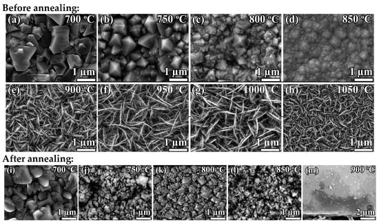
Figure 1.
SEM images of polycrystalline diamond films synthesized at fixed CH4 to total flow concentration = 40% and different substrate temperatures before (a–h) and after (i–m) air annealing.
At the fixed (40%) methane concentration, an increase in temperature from 700 to 750 °C firstly leads to a change in the faceting of diamond crystallites, which is evidence of the effect of CVD growth conditions on the texturing of PCD film. With a further increase in up to 850 °C, the film morphology transforms to nanocrystalline (NCD) diamond. In addition, at higher temperatures, only the deposition of graphite sheets occurs. Evidence of the more defective structure of PCD films grown at = 40% is their weakness to the annealing in air at a reasonable 590 °C. While the high-quality PCD films are usually stable in such conditions, for the PCD films grown at 40%, even the most well-faceted grains tend to be covered in etch pits—note in Figure 1 the degradation of diamond grains after annealing.
Figure 2 shows the surface morphologies of the diamond films deposited at two fixed substrate temperatures— = 800 ± 25 °C and = 900 ± 25 °C—and different .
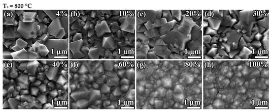
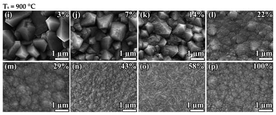
Figure 2.
SEM images of polycrystalline diamond films synthesized at substrate temperatures = 800 ± 25 °C (a–h) and 900 ± 25 °C (i–p) and different CH4 to total flow concentration .
Increasing the methane concentration leads to the MCD-to-NCD transition. However, the critical methane-concentration-to-NCD transition depends on the substrate temperature. The MCD-to-NCD transition occurs earlier at higher substrate temperatures. Thus, at = 900 °C, the critical point is in the region of = 20%, and, at = 800 °C, it shifts to the region of = 70%. Note that the synthesis regime at 900 °C and = 43% (Figure 2n) corresponds to the formation of an NCD film, while, in the first experimental series at the same temperature (Figure 1e), the NCD-to-graphite transition has already occurred. We explain this by the fact that, in the first series, the NCD-to-MCD transition occurred just between samples 850 and 900 °C (Figure 1d,e), i.e., 850–900 °C is the threshold temperature at = 40%. Thus, we consider the conditions of = 900 °C and = 40% to be a borderline between NCD and MCD regimes, so even slight deviations may lead to a change in the type of grown material. This means that there is no disagreement, taking into account the error in temperature control. In addition, note that, at 800 °C, even in pure methane gas (methane concentration of 100%), the deposition of NCD diamond films is possible.
3.2. X-ray Diffraction
The third series of experimental samples (grown at a fixed = 900 °C) was chosen for XRD analysis because it consists of texture PCD films and shows a transition from MCD to NCD. The X-ray diffraction patterns recorded in the standard θ/2θ scanning mode had a wide range of peaks caused by the decomposition of the X-ray tube spectrum on a single-crystal Si (100) substrate. A scanning mode was chosen with a deviation in the substrate plane from the position 2θ/2 by 3°, which makes it possible to eliminate the reflection from the substrate. The XRD pattern for the PCD films synthesized at substrate temperatures = 900 ± 25 °C and different CH4 concentration (Figure 3a) demonstrates four reflexes for diamond from crystallographic planes (111) at 2θ = 43.93°, (220) at 75.30°, (311) at 91.49°, (400) at 119.50° and (331) at 140.56°, and a wide set of peaks caused by the decomposition of the X-ray tube spectrum on a single-crystal Si (100) substrate in the region 2θ~69°.
Figure 3.
XRD patterns (a) and variation in texture coefficient (b) for the polycrystalline diamond films synthesized at substrate temperatures = 900 ± 25 °C and different . A wide set of peaks in region 2θ~69° belongs to the decomposition of the X-ray tube spectrum on Si (100) substrate.
The values of the texture coefficient were calculated. The effect of methane concentration on the texture coefficients along the (111), (220), (311), (400) and (331) planes is shown in Figure 3b. At standard methane concentration = 3% (111), (220) and (311) planes have the same value, which is higher than (400) and (331). With an increase in up to 22%, a sharp decrease in is observed. Note the simultaneous change in the film structure at the same concentration (Figure 3). With a further increase in , an increase in the reflection (220) is observed due to a further decrease in the reflection (111). Thus, films obtained at an ultrahigh methane concentration have a 220 texture.
3.3. Growth Rates
It is well known that the growth rate of diamond increases with the substrate temperature. We confirm an almost linear increase in the growth rate from 0.8 to 4.6 µm/h with elevation for the films deposited at = 40% (Figure 4a).
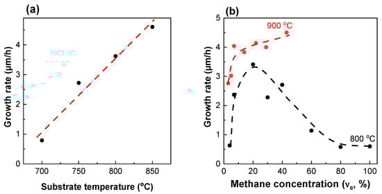
Figure 4.
Growth rates of polycrystalline diamond films synthesized at (a) fixed methane concentration = 40% and different substrate temperatures ; (b) fixed = 800 °C and = 900 °C with different concentrations. The lines are guides for the eye.
Despite the transition from MCD to NCD for the samples grown at an ultrahigh methane concentration, a decrease in the growth rate is observed (Figure 4b). For samples grown at = 800 °C, the growth rate increases from 0.6 µm/h at = 4% to 3.41 µm/h at = 20% and then decreases again to 0.6 µm/h at = 100%. For samples grown at = 900 °C, the same trend is observed, but with much higher growth rates and a shift in the critical point towards higher methane concentrations. The growth rate increases from 2.8 µm/h at = 3% to 4.1 µm/h at = 40% and then decreases to 2.1 µm/h at = 100%.
3.4. Raman Spectroscopy
The Raman spectra for the films deposited at fixed = 40% and different (700–1050 °C) before and after air anneal are shown in Figure 5.
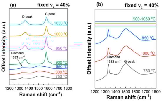
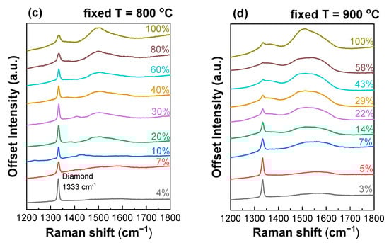
Figure 5.
(a,b) Raman spectra of polycrystalline diamond films synthesized at fixed CH4 to total flow concentration = 40% and different substrate temperatures before (a) and after (b) air anneal. (c,d) Raman spectra of polycrystalline diamond films synthesized at 800 ± 25 °C (c) and 900 ± 25 °C (d) and different concentrations.
The spectra reveal the following features common for polycrystalline diamond films: the arrow diamond peak at 1333 cm−1, two wide bands from trans-polyacetylene (t-PA) at 1140 and 1480 cm−1 and D- and G-peaks at 1350 and 1580 cm−1, respectively, from graphitic carbon. At fixed = 40% and substrate temperatures above = 900 °C, graphite wins in the competitive coprecipitation of diamond and graphite. Annealing in the air for 24 h at 590 °C leads to the complete removal of the sp2 phase of carbon, as confirmed by empty Raman spectra for these samples. Thus, at high methane concentrations, low synthesis temperatures promote diamond growth. At a temperature of 800 °C, the growth of the PCD diamond is possible at any concentration of methane from 4 to 100%. At a temperature of 900 °C, with an increase in the concentration of methane, the portion of the sp3 carbon phase to the sp2 phase decreases. Samples grown at 900 °C and = 29% and higher could be referred to as NCD diamond films.
The CVD conditions with = 40% and = 850 °C (sample in Figure 5a) are near the threshold at which diamond growth is no longer possible. At the same time, the sample obtained at 43% and 900 °C (Figure 3d) is NCD diamond. Given the accuracy of the temperature measurements, this is a normal observation for a threshold value. At a threshold temperature of 900 °C, an increase in the methane concentration above 43% did not lead to the formation of graphite. Thus, in this case, lower temperatures facilitated preserving the growth of the diamond phase instead of the formation of the continuous graphitic film.
3.5. sp2/sp3 Ratio
The sp2/sp3 ratio, expressed as the ratio of the sum of D- and G-peaks’ integrated intensities (areas under the bands) to that for the diamond Raman peak, is usually used to determine the quality of PCD films [57,58] and is shown in Figure 6. For this analysis, the diamond line at 1333 cm−1 was approximated by a Lorentzian profile, and the G- and D-peaks by two Gaussians.
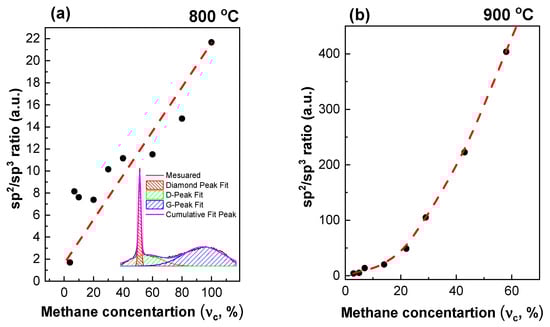
Figure 6.
The sp2/sp3 ratio for diamond films grown at substrate temperatures 800 °C (a) and 900 °C (b) depending on the methane concentration. The lines are guides for the eye. Insert: a typical example of Raman spectra deconvolution into the components (for sample = 5% and = 900 °C).
An increase in the substrate temperature or methane concentration leads to a decrease in the quality of the diamond. However, while, for 900 °C, this is an exponential trend, for 800 °C, it is almost linear. In addition, note an order of magnitude difference in the sp2/sp3 ratio between Figure 6a,b. Thus, at ultrahigh methane concentrations, temperature has more of a significance than methane concentration.
3.6. Diamond Raman Peak width
The dependence of the diamond Raman peak width on substrate temperatures and methane concentrations is shown in Figure 7. For this analysis, Raman spectra were recorded in a narrow frequency range and the diamond peak at 1333 cm−1 was approximated by a Lorentzian profile.
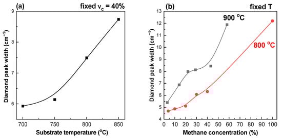
Figure 7.
Diamond Raman peak width (FWHM) for films grown: (a) at fixed CH4 to total flow concentration = 40% and different substrate temperatures; (b) at fixed substrate temperatures 800 and 900 °C depending on the methane concentration. The lines are guides for the eye.
An increase in the substrate temperature or methane concentration leads to a broadening of the diamond Raman peak. The full width on half magnitude (FWHM) increases from 5.9 cm−1 ( = 700 °C) to 8.7 cm−1 = 850 °C) for films grown at fixed = 40%. The FWHM increases from 4.7 cm−1 ( = 4%) to 12.2 cm−1 ( = 100%) for films grown at fixed = 800 °C. The FWHM increases from 5.4 cm−1 ( = 3%) to 11.9 cm−1 ( = 58%) for films grown at fixed = 900 °C. The broadening of the diamond peak may be associated with an increase in the number of microdeformations and defects in films grown at high methane concentrations and temperatures. The more defective structure of films grown at high temperatures is also confirmed by the reduced annealing resistance (see Figure 1i–l).
4. Conclusions
In our work, we demonstrated that diamond growth is possible even at ultrahigh (>20%) methane concentrations, including pure methane gas mixtures, which requires relatively low synthesis temperatures of < 800 °C to obtain MCD coatings. In general, low substrate temperatures facilitate the formation of higher-quality PCD films; however, this comes at the cost of lower growth rates. The PCD films grown at ultrahigh methane concentrations have a lower resistance to annealing in the air in comparison to higher-quality PCD films grown at low , which is evidence of a difference in the concentration of internal structural defects. Despite the possibility of growing diamond films at methane concentrations up to 100%, the growth rate of PCD coatings has a non-linear trend: for samples grown at = 800 °C, the growth rate increases from 0.6 µm/h at = 4% to 3.4 µm/h at = 20% and then decreases again to 0.6 µm/h at = 100%. With an increase in , an increase in the XRD reflection (220) is observed due to a decrease in the reflection (111). An increase in the substrate temperature or methane concentration leads to a broadening of the diamond Raman peak and an increase in the sp2/sp3 ratio of diamond films. The manipulation of the methane concentration and temperature has a complex and combined effect on the morphology, growth rate and phase composition of polycrystalline diamond films. The obtained results play an important role in the task of the control over the nature of the CVD-grown PCD material, which is essential for the precise and flexible production of diamond for various applications.
Author Contributions
Conceptualization, A.M. and V.S.; methodology, A.M. and V.S.; software, A.M. and I.T.; validation, A.M. and V.S.; formal analysis, V.V. and I.T.; investigation, A.M., S.S., I.T., V.V., and V.S.; resources, A.M. and I.T.; data curation, A.M. and I.T.; writing—original draft preparation, A.M.; writing—review and editing, A.M. and V.S.; visualization, A.M.; supervision, V.K.; project administration, A.M.; funding acquisition, A.M. All authors have read and agreed to the published version of the manuscript.
Funding
The work was supported by the grant of the Russian Science Foundation (Project No. 22-72-00082) https://rscf.ru/project/22-72-00082/ (accessed on 4 March 2023).
Institutional Review Board Statement
Not applicable.
Informed Consent Statement
Not applicable.
Data Availability Statement
Not applicable.
Acknowledgments
The authors would like to thank Soumen Mandal (Cardiff University, UK) for the provision of aqueous suspensions of nanodiamonds.
Conflicts of Interest
The authors declare no conflict of interest.
References
- Yue, Y.; Gao, Y.; Hu, W.; Xu, B.; Wang, J.; Zhang, X.; Zhang, Q.; Wang, Y.; Ge, B.; Yang, Z.; et al. Hierarchically structured diamond composite with exceptional toughness. Nature 2020, 582, 370–374. [Google Scholar] [CrossRef] [PubMed]
- Inyushkin, A.V.; Taldenkov, A.N.; Ralchenko, V.G.; Bolshakov, A.P.; Koliadin, A.V.; Katrusha, A.N. Thermal conductivity of high purity synthetic single crystal diamonds. Phys. Rev. B 2018, 97, 144305. [Google Scholar] [CrossRef]
- Inyushkin, A.V.; Taldenkov, A.N.; Ralchenko, V.G.; Shu, G.; Dai, B.; Bolshakov, A.P.; Khomich, A.A.; Ashkinazi, E.E.; Boldyrev, K.N.; Han, J.; et al. Thermal conductivity of pink CVD diamond: Influence of nitrogen-related centers. J. Appl. Phys. 2023, 133, 025102. [Google Scholar] [CrossRef]
- Sedov, V.; Martyanov, A.; Khomich, A.; Savin, S.; Voronov, V.; Khmelnitskiy, R.; Bolshakov, A.; Ralchenko, V. Co-deposition of diamond and β-SiC by microwave plasma CVD in H2-CH4-SiH4 gas mixtures. Diam. Relat. Mater. 2019, 98, 107520. [Google Scholar] [CrossRef]
- Ralchenko, V.; Sedov, V.; Martyanov, A.; Voronov, V.; Savin, S.; Khomich, A.; Shevchenko, M.; Bolshakov, A. Diamond-germanium composite films grown by microwave plasma CVD. Carbon 2022, 190, 10–21. [Google Scholar] [CrossRef]
- Sedov, V.S.; Martyanov, A.; Popovich, A.; Savin, S.; Sovyk, D.; Tiazhelov, I.; Pasternak, D.; Mandal, S.; Ralchenko, V.G. Microporous poly- and monocrystalline diamond films produced from chemical vapor deposited diamond–germanium composites. Nanoscale Adv. 2023, 5, 1307–1315. [Google Scholar] [CrossRef]
- Abdullah, M.F.; Hussin, M.R.M.; Ismail, M.A.; Sabli, S.K.W. Chip-level thermal management in GaN HEMT: Critical review on recent patents and inventions. Microelectron. Eng. 2023, 273, 111958. [Google Scholar] [CrossRef]
- Chernykh, M.; Andreev, A.; Ezubchenko, I.; Chernykh, I.; Mayboroda, I.; Kolobkova, E.; Khrapovitskaya, Y.V.; Grishchenko, J.; Perminov, P.; Sedov, V.; et al. GaN-based heterostructures with CVD diamond heat sinks: A new fabrication approach towards efficient electronic devices. Appl. Mater. Today 2022, 26, 101338. [Google Scholar] [CrossRef]
- Sedov, V.; Martyanov, A.; Altakhov, A.; Popovich, A.; Shevchenko, M.; Savin, S.; Zavedeev, E.; Zanaveskin, M.; Sinogeykin, A.; Ralchenko, V.; et al. Effect of Substrate Holder Design on Stress and Uniformity of Large-Area Polycrystalline Diamond Films Grown by Microwave Plasma-Assisted CVD. Coatings 2020, 10, 939. [Google Scholar] [CrossRef]
- Sedov, V.; Kuznetsov, S.; Martyanov, A.; Ralchenko, V. Luminescent diamond composites. Funct. Diam. 2022, 2, 53–63. [Google Scholar] [CrossRef]
- Najar, K.A.; Sheikh, N.A.; Butt, M.M.; Mushtaq, S.; Shah, M.A. Engineered Synthetic Diamond Film as a Protective Layer for Tribological and Machining Applications: A Review. J. Bio- Tribo-Corros. 2019, 5, 59. [Google Scholar] [CrossRef]
- Yan, G.; Wu, Y.; Cristea, D.; Liu, L.; Tierean, M.; Wang, Y.; Lu, F.; Wang, H.; Yuan, Z.; Munteanu, D.; et al. Mechanical properties and wear behavior of multi-layer diamond films deposited by hot-filament chemical vapor deposition. Appl. Surf. Sci. 2019, 494, 401–411. [Google Scholar] [CrossRef]
- Ashkihazi, E.; Sedov, V.; Sovyk, D.; Khomich, A.; Bolshakov, A.; Ryzhkov, S.; Vinogradov, D.; Ralchenko, V.; Konov, V. Plateholder design for deposition of uniform diamond coatings on WC-Co substrates by microwave plasma CVD for efficient turning application. Diam. Relat. Mater. 2017, 75, 169–175. [Google Scholar] [CrossRef]
- Moore, S.L.; Samudrala, G.K.; Catledge, S.A.; Vohra, Y.K. Rapid Growth of Nanocrystalline Diamond on Single Crystal Diamond for Studies on Materials under Extreme Conditions. Sci. Rep. 2018, 8, 1402. [Google Scholar] [CrossRef]
- Mallik, A.K. Polycrystalline Diamond Characterisations for High End Technologies. In Some Aspects of Diamonds in Scientific Research and High Technology; IntechOpen: London, UK, 2019. [Google Scholar]
- Guo, D.; Cai, N.; Wu, G.; Xie, F.; Tan, S.; Jiang, N.; Li, H. Improving Pressure–Velocity Limit of Mechanical Seal with Polycrystalline Diamond Coating. Appl. Sci. 2020, 10, 6090. [Google Scholar] [CrossRef]
- Williams, O. Nanocrystalline diamond. Diam. Relat. Mater. 2011, 20, 621–640. [Google Scholar] [CrossRef]
- Sedov, V.; Ralchenko, V.; Khomich, A.; Vlasov, I.; Vul, A.; Savin, S.; Goryachev, A.; Konov, V. Si-doped nano- and microcrystalline diamond films with controlled bright photoluminescence of silicon-vacancy color centers. Diam. Relat. Mater. 2015, 56, 23–28. [Google Scholar] [CrossRef]
- Fuentes-Fernandez, E.; Alcantar-Peña, J.; Lee, G.; Boulom, A.; Phan, H.; Smith, B.; Nguyen, T.; Sahoo, S.; Ruiz-Zepeda, F.; Arellano-Jimenez, M.; et al. Synthesis and characterization of microcrystalline diamond to ultrananocrystalline diamond films via Hot Filament Chemical Vapor Deposition for scaling to large area applications. Thin Solid Films 2016, 603, 62–68. [Google Scholar] [CrossRef]
- Sedov, V.S.; Martyanov, A.K.; Altakhov, A.S.; Savin, S.S.; Dobretsova, E.A.; Tiazhelov, I.A.; Pasternak, D.G.; Kaplunov, I.A.; Rogalin, V.E.; Ralchenko, V.G. Formation of Germanium–Vacancy Color Centers in CVD Diamond. J. Russ. Laser Res. 2022, 43, 503–508. [Google Scholar] [CrossRef]
- Karczemska, A.; Witkowski, D.; Ralchenko, V.; Bolshakov, A.; Sovyk, D.; Lysko, J.; Hassard, J. Diamond Microfluidic Devices Manufactured with the Replica Method. In Proceedings of the 2009 5th International Conference on Perspective Technologies and Methods in MEMS Design, Piscataway, NJ, USA, 22–24 April 2009; pp. 17–19. [Google Scholar]
- Mandal, S.; Yuan, C.; Massabuau, F.; Pomeroy, J.W.; Cuenca, J.; Bland, H.; Thomas, E.; Wallis, D.; Batten, T.; Morgan, D. Thick, Adherent Diamond Films on AlN with Low Thermal Barrier Resistance. ACS Appl. Mater. Interfaces 2019, 11, 40826–40834. [Google Scholar] [CrossRef] [PubMed]
- Zhou, Y.; Ramaneti, R.; Anaya, J.; Korneychuk, S.; Derluyn, J.; Sun, H.; Pomeroy, J.; Verbeeck, J.; Haenen, K.; Kuball, M. Thermal characterization of polycrystalline diamond thin film heat spreaders grown on GaN HEMTs. Appl. Phys. Lett. 2017, 111, 041901. [Google Scholar] [CrossRef]
- Kononenko, T.V.; Ralchenko, V.G.; Ashkinazi, E.E.; Polikarpov, M.; Ershov, P.; Kuznetsov, S.; Yunkin, V.; Snigireva, I.; Konov, V.I. Fabrication of polycrystalline diamond refractive X-ray lens by femtosecond laser processing. Appl. Phys. A 2016, 122, 152. [Google Scholar] [CrossRef]
- Salvatori, S.; Pettinato, S.; Piccardi, A.; Sedov, V.; Voronin, A.; Ralchenko, V. Thin Diamond Film on Silicon Substrates for Pressure Sensor Fabrication. Materials 2020, 13, 3697. [Google Scholar] [CrossRef] [PubMed]
- Pettinato, S.; Barettin, D.; Sedov, V.; Ralchenko, V.; Salvatori, S. Fabry-Perot Pressure Sensors Based on Polycrystalline Diamond Membranes. Materials 2021, 14, 1780. [Google Scholar] [CrossRef]
- Kononenko, T.; Sovyk, D.; Pivovarov, P.; Pavelyev, V.; Mezhenin, A.; Cherepanov, K.; Komlenok, M.; Sorochenko, V.; Khomich, A.; Pashinin, V.; et al. Fabrication of diamond diffractive optics for powerful CO2 lasers via replication of laser microstructures on silicon template. Diam. Relat. Mater. 2020, 101, 107656. [Google Scholar] [CrossRef]
- Ashkinazi, E.E.; Khmelnitskii, R.A.; Sedov, V.S.; Khomich, A.A.; Khomich, A.V.; Ralchenko, V.G. Morphology of Diamond Layers Grown on Different Facets of Single Crystal Diamond Substrates by a Microwave Plasma CVD in CH4-H2-N2 Gas Mixtures. Crystals 2017, 7, 166. [Google Scholar] [CrossRef]
- Podgursky, V.; Bogatov, A.; Yashin, M.; Viljus, M.; Bolshakov, A.; Sedov, V.; Volobujeva, O.; Mere, A.; Raadik, T.; Ralchenko, V. A comparative study of the growth dynamics and tribological properties of nanocrystalline diamond films deposited on the (110) single crystal diamond and Si(100) substrates. Diam. Relat. Mater. 2019, 92, 159–167. [Google Scholar] [CrossRef]
- Cicala, G.; Magaletti, V.; Carbone, G.; Senesi, G.S. Load sensitive super-hardness of nanocrystalline diamond coatings. Diam. Relat. Mater. 2020, 101, 107653. [Google Scholar] [CrossRef]
- Wang, H.; Yang, J.; Sun, F. Cutting performances of MCD, SMCD, NCD and MCD/NCD coated tools in high-speed milling of hot bending graphite molds. J. Mater. Process. Technol. 2020, 276, 116401. [Google Scholar] [CrossRef]
- Shenderova, O.A.; Gruen, D.M. Ultrananocrystalline Diamond: Synthesis, Properties and Applications; William Andrew: Norwich, NY, USA, 2012; ISBN 978-1-4377-3466-9. [Google Scholar]
- Auciello, O.; Sumant, A.V. Status Review of the Science and Technology of Ultrananocrystalline Diamond (UNCDTM) Films and Application to Multifunctional Devices. Diam. Relat. Mater. 2010, 19, 699–718. [Google Scholar] [CrossRef]
- Auciello, O.; Gurman, P.; Guglielmotti, M.B.; Olmedo, D.G.; Berra, A.; Saravia, M.J. Biocompatible ultrananocrystalline diamond coatings for implantable medical devices. MRS Bull. 2014, 39, 621–629. [Google Scholar] [CrossRef]
- Auciello, O.; Renou, S.; Kang, K.; Tasat, D.; Olmedo, D. A Biocompatible Ultrananocrystalline Diamond (UNCD) Coating for a New Generation of Dental Implants. Nanomaterials 2022, 12, 782. [Google Scholar] [CrossRef] [PubMed]
- Bhattacharyya, S.; Auciello, O.; Birrell, J.; Carlisle, J.A.; Curtiss, L.A.; Goyette, A.N.; Gruen, D.M.; Krauss, A.R.; Schlueter, J.A.; Sumant, A.V.; et al. Synthesis and characterization of highly-conducting nitrogen-doped ultrananocrystalline diamond films. Appl. Phys. Lett. 2001, 79, 1441–1443. [Google Scholar] [CrossRef]
- Ralchenko, V.; Pimenov, S.; Konov, V.; Khomich, A.; Saveliev, A.; Popovich, A.; Vlasov, I.; Zavedeev, E.; Bozhko, A.; Loubnin, E.; et al. Nitrogenated nanocrystalline diamond films: Thermal and optical properties. Diam. Relat. Mater. 2007, 16, 2067–2073. [Google Scholar] [CrossRef]
- Wanninayake, N.; Ai, Q.; Zhou, R.; Hoque, A.; Herrell, S.; Guzman, M.I.; Risko, C.; Kim, D.Y. Understanding the effect of host structure of nitrogen doped ultrananocrystalline diamond electrode on electrochemical carbon dioxide reduction. Carbon 2020, 157, 408–419. [Google Scholar] [CrossRef]
- Podgursky, V.; Bogatov, A.; Sedov, V.; Sildos, I.; Mere, A.; Viljus, M.; Buijnsters, J.; Ralchenko, V. Growth dynamics of nanocrystalline diamond films produced by microwave plasma enhanced chemical vapor deposition in methane/hydrogen/air mixture: Scaling analysis of surface morphology. Diam. Relat. Mater. 2015, 58, 172–179. [Google Scholar] [CrossRef]
- Mahoney, E.J.D.; Truscott, B.S.; Mushtaq, S.; Ashfold, M.N.R.; Mankelevich, Y.A. Spatially Resolved Optical Emission and Modeling Studies of Microwave-Activated Hydrogen Plasmas Operating under Conditions Relevant for Diamond Chemical Vapor Deposition. J. Phys. Chem. A 2018, 122, 8286–8300. [Google Scholar] [CrossRef]
- Tanei, H.; Nakamura, N.; Ogi, H.; Hirao, M.; Ikeda, R. Unusual Elastic Behavior of Nanocrystalline Diamond Thin Films. Phys. Rev. Lett. 2008, 100, 016804. [Google Scholar] [CrossRef] [PubMed]
- Sedov, V.; Martyanov, A.; Savin, S.; Zavedeev, E.; Kudryavtsev, O.; Bland, H.; Mandal, S.; Williams, O.; Ralchenko, V.; Konov, V. CVD synthesis of multi-layered polycrystalline diamond films with reduced roughness using time-limited injections of N2 gas. Diam. Relat. Mater. 2021, 114, 108333. [Google Scholar] [CrossRef]
- Erdemir, A.; Fenske, G.; Krauss, A.; Gruen, D.; McCauley, T.; Csencsits, R. Tribological properties of nanocrystalline diamond films. Surf. Coatings Technol. 1999, 120, 565–572. [Google Scholar] [CrossRef]
- Kulisch, W.; Popov, C. On the growth mechanisms of nanocrystalline diamond films. Phys. Status Solidi A 2006, 203, 203–219. [Google Scholar] [CrossRef]
- Bushuev, E.; Yurov, V.; Bolshakov, A.; Ralchenko, V.; Khomich, A.; Antonova, I.; Ashkinazi, E.; Shershulin, V.; Pashinin, V.; Konov, V. Express in situ measurement of epitaxial CVD diamond film growth kinetics. Diam. Relat. Mater. 2017, 72, 61–70. [Google Scholar] [CrossRef]
- Cuenca, J.A.; Sankaran, K.J.; Pobedinskas, P.; Panda, K.; Lin, I.-N.; Porch, A.; Haenen, K.; Williams, O.A. Microwave cavity perturbation of nitrogen doped nano-crystalline diamond films. Carbon 2019, 145, 740–750. [Google Scholar] [CrossRef]
- Sedov, V.; Popovich, A.; Linnik, S.; Martyanov, A.; Wei, J.; Zenkin, S.; Zavedeev, E.; Savin, S.; Gaydaychuk, A.; Li, C.; et al. Combined HF+MW CVD Approach for the Growth of Polycrystalline Diamond Films with Reduced Bow. Coatings 2023, 13, 380. [Google Scholar] [CrossRef]
- Song, X.; Lu, M.; Wang, H.; Wang, X.; Sun, F. Fracture mechanics of microcrystalline/nanocrystalline composited multilayer chemical vapor deposition self-standing diamond films. Ceram. Int. 2022, 48, 21909–21919. [Google Scholar] [CrossRef]
- Sedov, V.; Martyanov, A.; Khomich, A.; Savin, S.; Zavedeev, E.; Ralchenko, V. Deposition of diamond films on Si by microwave plasma CVD in varied CH4-H2 mixtures: Reverse nanocrystalline-to-microcrystalline structure transition at very high methane concentrations. Diam. Relat. Mater. 2020, 109, 108072. [Google Scholar] [CrossRef]
- Eto, H.; Tamou, Y.; Ohsawa, Y.; Kikuchi, N. TEM observations of diamond films prepared by microwave plasma CVD. Diam. Relat. Mater. 1992, 1, 373–379. [Google Scholar] [CrossRef]
- Wild, C.; Kohl, R.; Herres, N.; Müller-Sebert, W.; Koidl, P. Oriented CVD diamond films: Twin formation, structure and morphology. Diam. Relat. Mater. 1994, 3, 373–381. [Google Scholar] [CrossRef]
- Jeon, I.-D.; Park, C.J.; Kim, D.-Y.; Hwang, N.M. Effect of methane concentration on size of charged clusters in the hot filament diamond CVD process. J. Cryst. Growth 2001, 223, 6–14. [Google Scholar] [CrossRef]
- Gines, L.; Mandal, S.; Cheng, C.L.; Sow, M.; Williams, O.A. Positive zeta potential of nanodiamonds. Nanoscale 2017, 9, 12549–12555. [Google Scholar] [CrossRef]
- Mandal, S. Nucleation of diamond films on heterogeneous substrates: A review. RSC Adv. 2021, 11, 10159–10182. [Google Scholar] [CrossRef]
- Nasser, S.A.; Afify, H.H.; El-Hakim, S.A.; Zayed, M.K. Structural and physical properties of sprayed copper–zinc oxide films. Thin Solid Films 1998, 315, 327–335. [Google Scholar] [CrossRef]
- Paprocki, K.; Fabisiak, K.; Łoś, S.; Winiecki, J.; Malinowski, P.; Fabisiak, R.; Franków, W. Morphological, cathodoluminescence and thermoluminescence studies of defects in diamond films grown by HF CVD technique. Opt. Mater. 2020, 99, 109506. [Google Scholar] [CrossRef]
- Ferreira, N.G.; Leite, N.F.; Corat, E.J.; Trava-Airoldi, V.J.; Abramof, E. Analysis of residual stress in diamond films by x-ray diffraction and micro-Raman spectroscopy. J. Appl. Phys. 2002, 91, 2466–2472. [Google Scholar] [CrossRef]
- Ballutaud, D.; Jomard, F.; Kociniewski, T.; Rzepka, E.; Girard, H.; Saada, S. Sp3/Sp2 Character of the Carbon and Hydrogen Configuration in Micro-and Nanocrystalline Diamond. Diam. Relat. Mater. 2008, 17, 451–456. [Google Scholar] [CrossRef]
Disclaimer/Publisher’s Note: The statements, opinions and data contained in all publications are solely those of the individual author(s) and contributor(s) and not of MDPI and/or the editor(s). MDPI and/or the editor(s) disclaim responsibility for any injury to people or property resulting from any ideas, methods, instructions or products referred to in the content. |
© 2023 by the authors. Licensee MDPI, Basel, Switzerland. This article is an open access article distributed under the terms and conditions of the Creative Commons Attribution (CC BY) license (https://creativecommons.org/licenses/by/4.0/).